Embed Size (px)
Citation preview
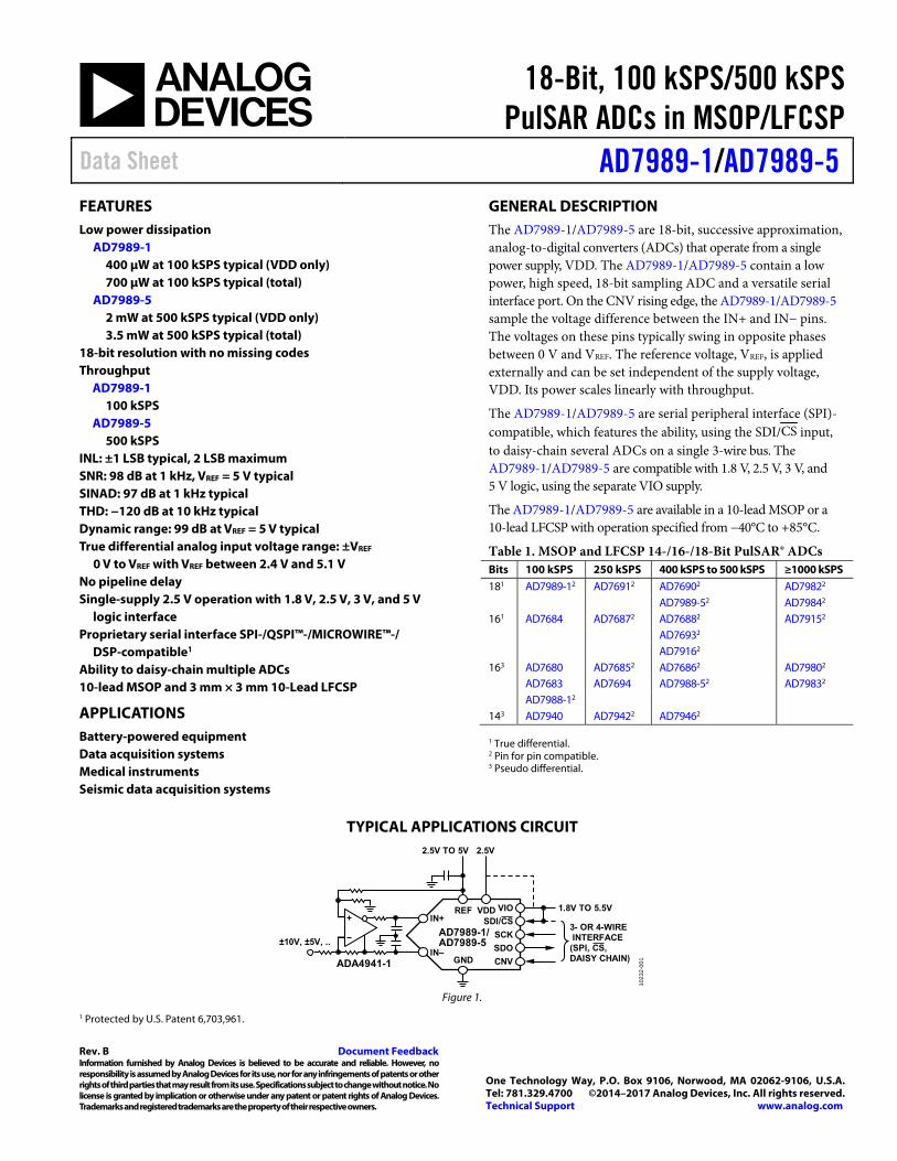
18-Bit, 100 kSPS/500 kSPSPulSAR ADCs in MSOP/LFCSP
Data Sheet AD7989-1/AD7989-5
Rev. B Document Feedback Information furnished by Analog Devices is believed to be accurate and reliable. However, no responsibility is assumed by Analog Devices for its use, nor for any infringements of patents or other rights of third parties that may result from its use. Specifications subject to change without notice. No license is granted by implication or otherwise under any patent or patent rights of Analog Devices. Trademarks and registered trademarks are the property of their respective owners.
One Technology Way, P.O. Box 9106, Norwood, MA 02062-9106, U.S.A.Tel: 781.329.4700 ©2014–2017 Analog Devices, Inc. All rights reserved. Technical Support www.analog.com
FEATURES Low power dissipation
AD7989-1 400 μW at 100 kSPS typical (VDD only) 700 μW at 100 kSPS typical (total)
AD7989-5 2 mW at 500 kSPS typical (VDD only) 3.5 mW at 500 kSPS typical (total)
18-bit resolution with no missing codes Throughput
AD7989-1 100 kSPS
AD7989-5 500 kSPS
INL: ±1 LSB typical, 2 LSB maximum SNR: 98 dB at 1 kHz, VREF = 5 V typical SINAD: 97 dB at 1 kHz typical THD: −120 dB at 10 kHz typical Dynamic range: 99 dB at VREF = 5 V typical True differential analog input voltage range: ±VREF
0 V to VREF with VREF between 2.4 V and 5.1 V No pipeline delay Single-supply 2.5 V operation with 1.8 V, 2.5 V, 3 V, and 5 V
logic interface Proprietary serial interface SPI-/QSPI™-/MICROWIRE™-/
DSP-compatible1 Ability to daisy-chain multiple ADCs 10-lead MSOP and 3 mm × 3 mm 10-Lead LFCSP
APPLICATIONS Battery-powered equipment Data acquisition systems Medical instruments Seismic data acquisition systems
GENERAL DESCRIPTION The AD7989-1/AD7989-5 are 18-bit, successive approximation, analog-to-digital converters (ADCs) that operate from a single power supply, VDD. The AD7989-1/AD7989-5 contain a low power, high speed, 18-bit sampling ADC and a versatile serial interface port. On the CNV rising edge, the AD7989-1/AD7989-5 sample the voltage difference between the IN+ and IN− pins. The voltages on these pins typically swing in opposite phases between 0 V and VREF. The reference voltage, VREF, is applied externally and can be set independent of the supply voltage, VDD. Its power scales linearly with throughput.
The AD7989-1/AD7989-5 are serial peripheral interface (SPI)-compatible, which features the ability, using the SDI/CS input, to daisy-chain several ADCs on a single 3-wire bus. The AD7989-1/AD7989-5 are compatible with 1.8 V, 2.5 V, 3 V, and 5 V logic, using the separate VIO supply.
The AD7989-1/AD7989-5 are available in a 10-lead MSOP or a 10-lead LFCSP with operation specified from −40°C to +85°C.
Table 1. MSOP and LFCSP 14-/16-/18-Bit PulSAR® ADCs Bits 100 kSPS 250 kSPS 400 kSPS to 500 kSPS ≥1000 kSPS
181 AD7989-12 AD76912 AD76902 AD79822 AD7989-52 AD79842 161 AD7684 AD76872 AD76882 AD79152 AD76932 AD79162 163 AD7680 AD76852 AD76862 AD79802 AD7683 AD7694 AD7988-52 AD79832 AD7988-12 143 AD7940 AD79422 AD79462 1 True differential. 2 Pin for pin compatible. 3 Pseudo differential.
TYPICAL APPLICATIONS CIRCUIT
Figure 1.
1 Protected by U.S. Patent 6,703,961.
REF
GND
VDDIN+
IN–
VIO
SDI/CS
SCK
SDO
CNV
1.8V TO 5.5V
ADA4941-1
3- OR 4-WIRE INTERFACE(SPI, CS,DAISY CHAIN)
2.5V TO 5V 2.5V
±10V, ±5V, ..AD7989-1/AD7989-5
1023
2-00
1
AD7989-1/AD7989-5 Data Sheet
Rev. B | Page 2 of 24
TABLE OF CONTENTS Features .....................................................................................1
Applications...............................................................................1
General Description ..................................................................1
Typical Applications Circuit ......................................................1
Revision History ........................................................................2
Specifications .............................................................................3
Timing Specifications ............................................................5
Absolute Maximum Ratings ......................................................7
ESD Caution ..........................................................................7
Pin Configurations and Function Descriptions .........................8
Typical Performance Characteristics .........................................9
Terminology ............................................................................12
Theory of Operation ................................................................13
Circuit Information .............................................................13
Converter Operation............................................................13
Typical Connection Diagram ...............................................14
Analog Inputs ...................................................................... 15
Driver Amplifier Choice ...................................................... 15
Single-Ended to Differential Driver ..................................... 16
Voltage Reference Input ....................................................... 16
Power Supply ....................................................................... 16
Digital Interface ................................................................... 16
CS Mode, 3-Wire ................................................................. 17
CS Mode, 4-Wire ................................................................. 18
Chain Mode ......................................................................... 19
Applications Information ........................................................ 20
Interfacing to Blackfin® DSP ................................................ 20
Layout .................................................................................. 20
Evaluating AD7989-1/AD7989-5 Performance....................... 21
Outline Dimensions ................................................................ 22
Ordering Guide ................................................................... 23
REVISION HISTORY 1/2017—Rev. A to Rev. B Change to Table 1 ......................................................................1 Changed VIO = 2.3 V to 5.5 V to VIO = 1.71 V to 5.5 V ...........3 Changes to Table 2 .....................................................................3 Changed VIO = 2.3 V to 5.5 V to VIO = 1.71 V to 5.5 V ...........4 Deleted VIO Range Parameter, Table 3......................................4 Changes to Table 4 .....................................................................5 Added Table 5; Renumbered Sequentially .................................6 Changes to Figure 9 ...................................................................9 Change to Terminology Section ..............................................12 Changes to Figure 26 ...............................................................14 Changes to Table 9 ...................................................................15
Change to Single-Ended to Differential Driver Section Title... 16 Changes to Figure 32 ............................................................... 17 Changes to Figure 34 ............................................................... 18 Changes to Ordering Guide..................................................... 23 7/2014—Rev. 0 to Rev. A Changes to Features Section ...................................................... 1 Changes to Table 1..................................................................... 1 Changes to Table 8................................................................... 15 1/2014—Revision 0: Initial Version
Data Sheet AD7989-1/AD7989-5
Rev. B | Page 3 of 24
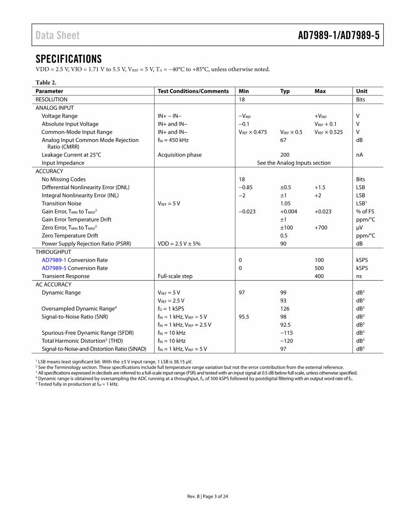
SPECIFICATIONS VDD = 2.5 V, VIO = 1.71 V to 5.5 V, VREF = 5 V, TA = −40°C to +85°C, unless otherwise noted.
Table 2. Parameter Test Conditions/Comments Min Typ Max Unit RESOLUTION 18 Bits ANALOG INPUT
Voltage Range IN+ − IN− −VREF +VREF V Absolute Input Voltage IN+ and IN− −0.1 VREF + 0.1 V Common-Mode Input Range IN+ and IN− VREF × 0.475 VREF × 0.5 VREF × 0.525 V Analog Input Common Mode Rejection
Ratio (CMRR) fIN = 450 kHz 67 dB
Leakage Current at 25°C Acquisition phase 200 nA Input Impedance See the Analog Inputs section
ACCURACY No Missing Codes 18 Bits Differential Nonlinearity Error (DNL) −0.85 ±0.5 +1.5 LSB Integral Nonlinearity Error (INL) −2 ±1 +2 LSB Transition Noise VREF = 5 V 1.05 LSB1 Gain Error, TMIN to TMAX
2 −0.023 +0.004 +0.023 % of FS Gain Error Temperature Drift ±1 ppm/°C Zero Error, TMIN to TMAX
2 ±100 +700 μV Zero Temperature Drift 0.5 ppm/°C Power Supply Rejection Ratio (PSRR) VDD = 2.5 V ± 5% 90 dB
THROUGHPUT AD7989-1 Conversion Rate 0 100 kSPS AD7989-5 Conversion Rate 0 500 kSPS Transient Response Full-scale step 400 ns
AC ACCURACY Dynamic Range VREF = 5 V 97 99 dB3 VREF = 2.5 V 93 dB3 Oversampled Dynamic Range4 fO = 1 kSPS 126 dB3 Signal-to-Noise Ratio (SNR) fIN = 1 kHz, VREF = 5 V 95.5 98 dB3 fIN = 1 kHz, VREF = 2.5 V 92.5 dB3 Spurious-Free Dynamic Range (SFDR) fIN = 10 kHz −115 dB3 Total Harmonic Distortion5 (THD) fIN = 10 kHz −120 dB3 Signal-to-Noise-and-Distortion Ratio (SINAD) fIN = 1 kHz, VREF = 5 V 97 dB3
1 LSB means least significant bit. With the ±5 V input range, 1 LSB is 38.15 μV. 2 See the Terminology section. These specifications include full temperature range variation but not the error contribution from the external reference. 3 All specifications expressed in decibels are referred to a full-scale input range (FSR) and tested with an input signal at 0.5 dB below full scale, unless otherwise specified. 4 Dynamic range is obtained by oversampling the ADC running at a throughput, fS, of 500 kSPS followed by postdigital filtering with an output word rate of fO. 5 Tested fully in production at fIN = 1 kHz.
AD7989-1/AD7989-5 Data Sheet
Rev. B | Page 4 of 24
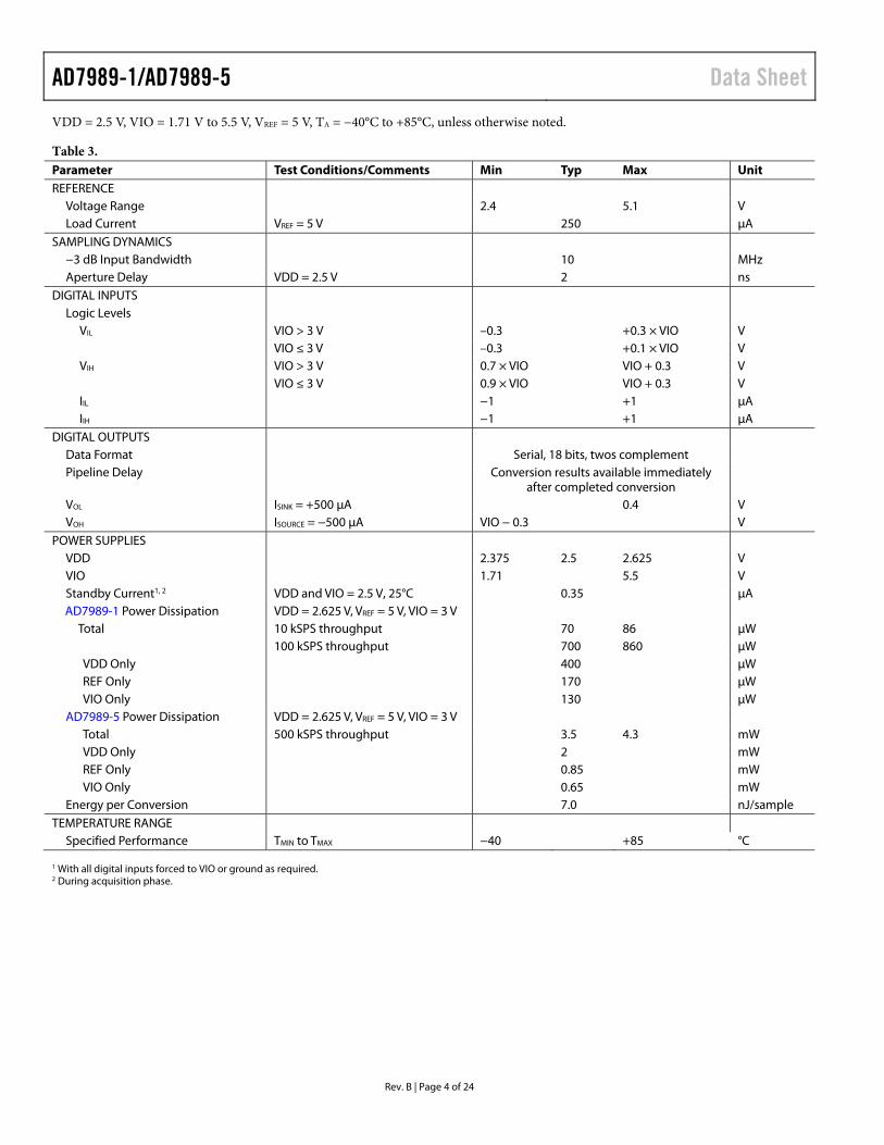
VDD = 2.5 V, VIO = 1.71 V to 5.5 V, VREF = 5 V, TA = −40°C to +85°C, unless otherwise noted.
Table 3. Parameter Test Conditions/Comments Min Typ Max Unit REFERENCE
Voltage Range 2.4 5.1 V Load Current VREF = 5 V 250 μA
SAMPLING DYNAMICS −3 dB Input Bandwidth 10 MHz Aperture Delay VDD = 2.5 V 2 ns
DIGITAL INPUTS Logic Levels
VIL VIO > 3 V –0.3 +0.3 × VIO V VIO ≤ 3 V –0.3 +0.1 × VIO V VIH VIO > 3 V 0.7 × VIO VIO + 0.3 V VIO ≤ 3 V 0.9 × VIO VIO + 0.3 V IIL −1 +1 μA IIH −1 +1 μA
DIGITAL OUTPUTS Data Format Serial, 18 bits, twos complement Pipeline Delay Conversion results available immediately
after completed conversion
VOL ISINK = +500 μA 0.4 V VOH ISOURCE = −500 μA VIO − 0.3 V
POWER SUPPLIES VDD 2.375 2.5 2.625 V VIO 1.71 5.5 V Standby Current1, 2 VDD and VIO = 2.5 V, 25°C 0.35 μA AD7989-1 Power Dissipation VDD = 2.625 V, VREF = 5 V, VIO = 3 V
Total 10 kSPS throughput 70 86 μW 100 kSPS throughput 700 860 μW VDD Only 400 μW REF Only 170 μW VIO Only 130 μW
AD7989-5 Power Dissipation VDD = 2.625 V, VREF = 5 V, VIO = 3 V Total 500 kSPS throughput 3.5 4.3 mW VDD Only 2 mW REF Only 0.85 mW VIO Only 0.65 mW
Energy per Conversion 7.0 nJ/sample TEMPERATURE RANGE
Specified Performance TMIN to TMAX −40 +85 °C 1 With all digital inputs forced to VIO or ground as required. 2 During acquisition phase.
Data Sheet AD7989-1/AD7989-5
Rev. B | Page 5 of 24
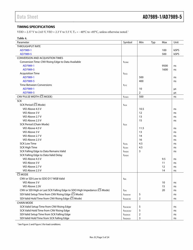
TIMING SPECIFICATIONS VDD = 2.37 V to 2.63 V, VIO = 2.3 V to 5.5 V, TA = −40°C to +85°C, unless otherwise noted.1
Table 4. Parameter Symbol Min Typ Max Unit THROUGHPUT RATE
AD7989-1 100 kSPS AD7989-5 500 kSPS
CONVERSION AND ACQUISITION TIMES Conversion Time: CNV Rising Edge to Data Available tCONV
AD7989-1 9500 ns AD7989-5 1600 ns
Acquisition Time tACQ AD7989-1 500 ns AD7989-5 400 ns
Time Between Conversions tCYC AD7989-1 10 μs AD7989-5 2 μs
CNV PULSE WIDTH (CS MODE) tCNVH 500 ns
SCK SCK Period (CS Mode) tSCK
VIO Above 4.5 V 10.5 ns VIO Above 3 V 12 ns VIO Above 2.7 V 13 ns VIO Above 2.3 V 15 ns
SCK Period (Chain Mode) tSCK VIO Above 4.5 V 11.5 ns VIO Above 3 V 13 ns VIO Above 2.7 V 14 ns VIO Above 2.3 V 16 ns
SCK Low Time tSCKL 4.5 ns SCK High Time tSCKH 4.5 ns SCK Falling Edge to Data Remains Valid tHSDO 3 ns SCK Falling Edge to Data Valid Delay tDSDO
VIO Above 4.5 V 9.5 ns VIO Above 3 V 11 ns VIO Above 2.7 V 12 ns VIO Above 2.3 V 14 ns
CS MODE
CNV or SDI Low to SDO D17 MSB Valid tEN VIO Above 3 V 10 ns VIO Above 2.3V 15 ns
CNV or SDI High or Last SCK Falling Edge to SDO High Impedance (CS Mode) tDIS 20 ns
SDI Valid Setup Time from CNV Rising Edge (CS Mode) tSSDICNV 5 ns
SDI Valid Hold Time from CNV Rising Edge (CS Mode) tHSDICNV 2 ns
CHAIN MODE SCK Valid Setup Time from CNV Rising Edge tSSCKCNV 5 ns SCK Valid Hold Time from CNV Rising Edge tHSCKCNV 5 ns SDI Valid Setup Time from SCK Falling Edge tSSDISCK 2 ns SDI Valid Hold Time from SCK Falling Edge tHSDISCK 3 ns
1 See Figure 2 and Figure 3 for load conditions.
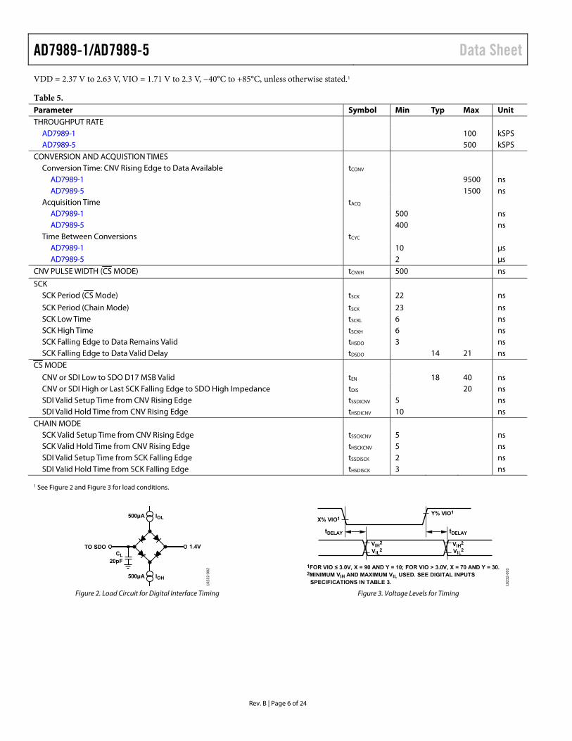
AD7989-1/AD7989-5 Data Sheet
Rev. B | Page 6 of 24
VDD = 2.37 V to 2.63 V, VIO = 1.71 V to 2.3 V, −40°C to +85°C, unless otherwise stated.1
Table 5. Parameter Symbol Min Typ Max Unit THROUGHPUT RATE
AD7989-1 100 kSPS AD7989-5 500 kSPS
CONVERSION AND ACQUISTION TIMES Conversion Time: CNV Rising Edge to Data Available tCONV
AD7989-1 9500 ns AD7989-5 1500 ns
Acquisition Time tACQ AD7989-1 500 ns AD7989-5 400 ns
Time Between Conversions tCYC AD7989-1 10 μs AD7989-5 2 μs
CNV PULSE WIDTH (CS MODE) tCNVH 500 ns
SCK SCK Period (CS Mode) tSCK 22 ns
SCK Period (Chain Mode) tSCK 23 ns SCK Low Time tSCKL 6 ns SCK High Time tSCKH 6 ns SCK Falling Edge to Data Remains Valid tHSDO 3 ns SCK Falling Edge to Data Valid Delay tDSDO 14 21 ns
CS MODE
CNV or SDI Low to SDO D17 MSB Valid tEN 18 40 ns CNV or SDI High or Last SCK Falling Edge to SDO High Impedance tDIS 20 ns SDI Valid Setup Time from CNV Rising Edge tSSDICNV 5 ns SDI Valid Hold Time from CNV Rising Edge tHSDICNV 10 ns
CHAIN MODE SCK Valid Setup Time from CNV Rising Edge tSSCKCNV 5 ns SCK Valid Hold Time from CNV Rising Edge tHSCKCNV 5 ns SDI Valid Setup Time from SCK Falling Edge tSSDISCK 2 ns SDI Valid Hold Time from SCK Falling Edge tHSDISCK 3 ns
1 See Figure 2 and Figure 3 for load conditions.
Figure 2. Load Circuit for Digital Interface Timing
Figure 3. Voltage Levels for Timing
500µA IOL
500µA IOH
1.4VTO SDOCL
20pF
1023
2-00
2
X% VIO1Y% VIO1
VIH2
VIL2VIL
2VIH
2
tDELAY tDELAY
1FOR VIO ≤ 3.0V, X = 90 AND Y = 10; FOR VIO > 3.0V, X = 70 AND Y = 30.2MINIMUM VIH AND MAXIMUM VIL USED. SEE DIGITAL INPUTS SPECIFICATIONS IN TABLE 3. 10
232-
003
Data Sheet AD7989-1/AD7989-5
Rev. B | Page 7 of 24
ABSOLUTE MAXIMUM RATINGS Table 6. Parameter Rating Analog Inputs
IN+, IN− to GND1 −0.3 V to VREF + 0.3 V or ±130 mA Supply Voltage
REF, VIO to GND −0.3 V to +6.0 V VDD to GND −0.3 V to +3.0 V VDD to VIO +3 V to −6 V
Digital Inputs to GND −0.3 V to VIO + 0.3 V Digital Output to GND −0.3 V to VIO + 0.3 V Storage Temperature Range −65°C to +150°C Junction Temperature 150°C θJA Thermal Impedance
10-Lead MSOP 200°C/W 10-Lead LFCSP 48.7°C/W
θJC Thermal Impedance 10-Lead MSOP 44°C/W 10-Lead LFCSP 2.96°C/W
Reflow Soldering JEDEC Standard (J-STD-020) 1 See the Analog Inputs section for an explanation of IN+ and IN−.
Stresses at or above those listed under Absolute Maximum Ratings may cause permanent damage to the product. This is a stress rating only; functional operation of the product at these or any other conditions above those indicated in the operational section of this specification is not implied. Operation beyond the maximum operating conditions for extended periods may affect product reliability.
ESD CAUTION
AD7989-1/AD7989-5 Data Sheet
Rev. B | Page 8 of 24
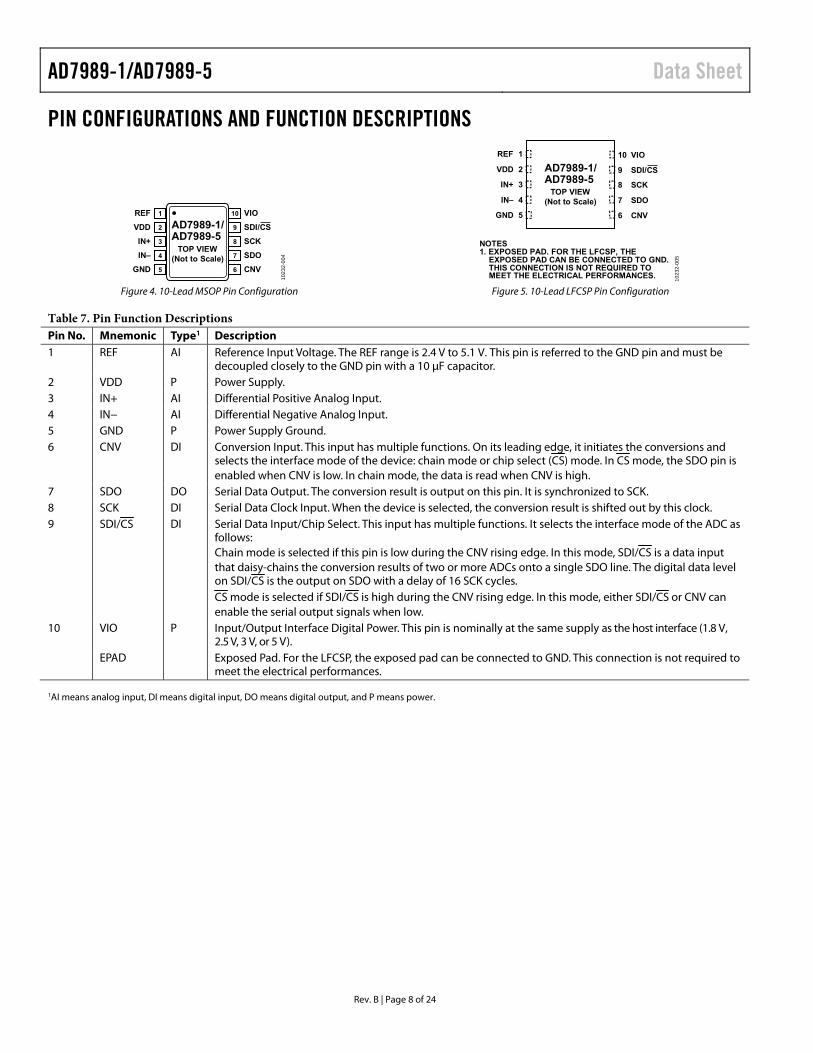
PIN CONFIGURATIONS AND FUNCTION DESCRIPTIONS
Figure 4. 10-Lead MSOP Pin Configuration Figure 5. 10-Lead LFCSP Pin Configuration
Table 7. Pin Function Descriptions Pin No. Mnemonic Type1 Description 1 REF AI Reference Input Voltage. The REF range is 2.4 V to 5.1 V. This pin is referred to the GND pin and must be
decoupled closely to the GND pin with a 10 μF capacitor. 2 VDD P Power Supply. 3 IN+ AI Differential Positive Analog Input. 4 IN− AI Differential Negative Analog Input. 5 GND P Power Supply Ground. 6 CNV DI Conversion Input. This input has multiple functions. On its leading edge, it initiates the conversions and
selects the interface mode of the device: chain mode or chip select (CS) mode. In CS mode, the SDO pin is enabled when CNV is low. In chain mode, the data is read when CNV is high.
7 SDO DO Serial Data Output. The conversion result is output on this pin. It is synchronized to SCK. 8 SCK DI Serial Data Clock Input. When the device is selected, the conversion result is shifted out by this clock. 9 SDI/CS DI Serial Data Input/Chip Select. This input has multiple functions. It selects the interface mode of the ADC as
follows: Chain mode is selected if this pin is low during the CNV rising edge. In this mode, SDI/CS is a data input that daisy-chains the conversion results of two or more ADCs onto a single SDO line. The digital data level on SDI/CS is the output on SDO with a delay of 16 SCK cycles. CS mode is selected if SDI/CS is high during the CNV rising edge. In this mode, either SDI/CS or CNV can enable the serial output signals when low.
10 VIO P Input/Output Interface Digital Power. This pin is nominally at the same supply as the host interface (1.8 V, 2.5 V, 3 V, or 5 V).
EPAD Exposed Pad. For the LFCSP, the exposed pad can be connected to GND. This connection is not required to meet the electrical performances.
1AI means analog input, DI means digital input, DO means digital output, and P means power.
REF 1
VDD 2
IN+ 3
IN– 4
GND 5
VIO10
SDI/CS9
SCK8
SDO7
CNV6
AD7989-1/AD7989-5
TOP VIEW(Not to Scale)
1023
2-00
4
NOTES1. EXPOSED PAD. FOR THE LFCSP, THE EXPOSED PAD CAN BE CONNECTED TO GND. THIS CONNECTION IS NOT REQUIRED TO MEET THE ELECTRICAL PERFORMANCES.
1REF
2VDD
3IN+
4IN–
5GND
10 VIO
9 SDI/CS
8 SCK
7 SDO
6 CNV
AD7989-1/AD7989-5
TOP VIEW(Not to Scale)
1023
2-00
5
Data Sheet AD7989-1/AD7989-5
Rev. B | Page 9 of 24
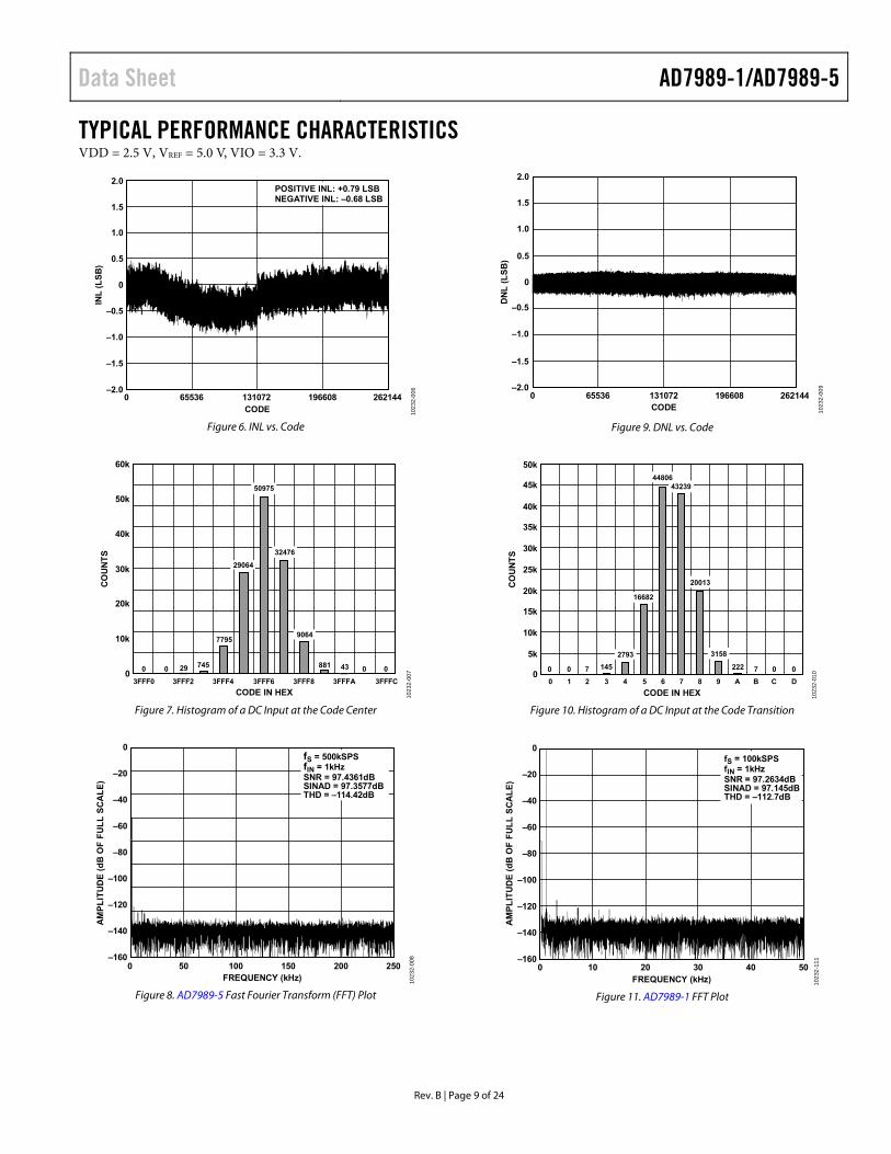
TYPICAL PERFORMANCE CHARACTERISTICS VDD = 2.5 V, VREF = 5.0 V, VIO = 3.3 V.
Figure 6. INL vs. Code
Figure 7. Histogram of a DC Input at the Code Center
Figure 8. AD7989-5 Fast Fourier Transform (FFT) Plot
Figure 9. DNL vs. Code
Figure 10. Histogram of a DC Input at the Code Transition
Figure 11. AD7989-1 FFT Plot
2.0
1.5
1.0
0.5
0
–0.5
–1.0
–1.5
–2.0
INL
(L
SB
)
0 65536 131072 196608 262144CODE
POSITIVE INL: +0.79 LSBNEGATIVE INL: –0.68 LSB
1023
2-00
6
60k
50k
40k
30k
20k
10k
0
CO
UN
TS
3FFF0 3FFF2 3FFF4 3FFF6 3FFF8 3FFFA 3FFFC
CODE IN HEX
0 0 29 745 881 43 00
7795
29064
50975
32476
9064
1023
2-00
7
0
–20
–40
–60
–80
–100
–120
–140
–1600 50 100 150 200 250
FREQUENCY (kHz)
AM
PL
ITU
DE
(d
B O
F F
UL
L S
CA
LE
)
1023
2-00
8
fS = 500kSPSfIN = 1kHzSNR = 97.4361dBSINAD = 97.3577dBTHD = –114.42dB
2.0
1.5
1.0
0.5
0
–0.5
–1.0
–1.5
–2.00 65536 131072 196608 262144
CODE
DN
L (
LS
B)
1023
2-00
9
50k
45k
40k
35k
30k
25k
0
CO
UN
TS
0 1 2 3 4 5 6 7 8 9 A D
CODE IN HEX
0 0 7 145 7 0 0
20k
15k
10k
5k
222
CB
16682
4480643239
20013
31582793
1023
2-01
0
0
–20
–40
–60
–80
–100
–120
–140
–1600 10 20 30 40 50
FREQUENCY (kHz)
AM
PL
ITU
DE
(d
B O
F F
UL
L S
CA
LE
)
1023
2-11
1
fS = 100kSPSfIN = 1kHzSNR = 97.2634dBSINAD = 97.145dBTHD = –112.7dB
AD7989-1/AD7989-5 Data Sheet
Rev. B | Page 10 of 24
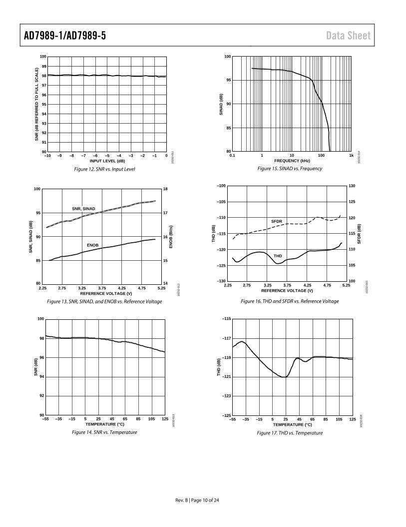
Figure 12. SNR vs. Input Level
Figure 13. SNR, SINAD, and ENOB vs. Reference Voltage
Figure 14. SNR vs. Temperature
Figure 15. SINAD vs. Frequency
Figure 16. THD and SFDR vs. Reference Voltage
Figure 17. THD vs. Temperature
100
99
98
97
96
95
94
93
92
91
90–10 –9 –8 –7 –6 –5 –4 –3 –2 –1 0
INPUT LEVEL (dB)
SNR
(dB
REF
ERR
ED T
O F
ULL
SC
ALE
)
1023
2-01
1
100
95
90
85
80
SNR
, SIN
AD
(dB
)
2.25 2.75 3.25 3.75 4.25 4.75 5.25REFERENCE VOLTAGE (V)
18
17
16
15
14
ENO
B (B
its)
ENOB
SNR, SINAD
1023
2-01
2
100
98
96
94
92
90
SNR
(dB
)
–55 –35 –15 5 25 45 65 85 105 125TEMPERATURE (°C) 10
232-
013
100
95
90
85
800.1 1 10 100 1k
FREQUENCY (kHz)
SIN
AD
(dB
)
1023
2-01
4
–100
–105
–110
–115
–120
–125
–130
THD
(dB
)
2.25 2.75 3.25 3.75 4.25 4.75 5.25REFERENCE VOLTAGE (V)
130
125
120
115
110
105
100
SFD
R (d
B)
THD
SFDR
1023
2-01
5
–115
–117
–119
–121
–123
–125
THD
(dB
)
–55 –35 –15 5 25 45 65 85 105 125TEMPERATURE (°C) 10
232-
016
Data Sheet AD7989-1/AD7989-5
Rev. B | Page 11 of 24
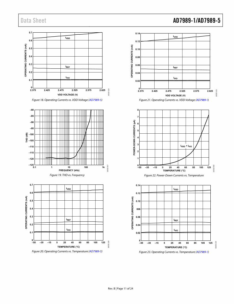
Figure 18. Operating Currents vs. VDD Voltage (AD7989-5)
Figure 19. THD vs. Frequency
Figure 20. Operating Currents vs. Temperature (AD7989-5)
Figure 21. Operating Currents vs. VDD Voltage (AD7989-1)
Figure 22. Power-Down Currents vs. Temperature
Figure 23. Operating Currents vs. Temperature (AD7989-1)
0.7
0.6
0.5
0.4
0.3
0.2
0.1
0
VDD VOLTAGE (V)
IVDD
IREF
IVIO
OP
ER
AT
ING
CU
RR
EN
TS
(m
A)
2.375 2.425 2.475 2.525 2.575 2.625
1023
2-11
8–80
–85
–90
–95
–100
–105
–110
–115
–120
–1250.1 1 10 100 1k
FREQUENCY (kHz)
TH
D (
dB
)
1023
2-01
7
0.7
0.6
0.5
0.4
0.3
0.2
0.1
0
OP
ER
AT
ING
CU
RR
EN
TS
(m
A)
IVDD
IREF
IVIO
TEMPERATURE (°C)
–55 –35 –15 5 25 45 65 85 105 125
1023
2-12
0
0.14
0.12
0.10
0.08
0.06
0.04
0.02
0
VDD VOLTAGE (V)
IVDD
IREF
IVIO
OP
ER
AT
ING
CU
RR
EN
TS
(m
A)
2.375 2.425 2.475 2.525 2.575 2.625
1023
2-12
1
8
7
6
5
4
3
2
1
0
PO
WE
R-D
OW
N C
UR
RE
NT
S (
µA
)
–55 –35 –15 5 25TEMPERATURE (°C)
45 65 85 105 125
IVDD + IVIO
1023
2-01
8
0.14
0.12
0.10
008
0.06
0.04
0.02
0
OP
ER
AT
ING
CU
RR
EN
TS
(m
A)
IVDD
IREF
IVIO
TEMPERATURE (°C)
–55 –35 –15 5 25 45 65 85 105 125
1023
3-12
3
AD7989-1/AD7989-5 Data Sheet
Rev. B | Page 12 of 24
TERMINOLOGY Integral Nonlinearity Error (INL) INL refers to the deviation of each individual code from a line drawn from negative full scale through positive full scale. The point used as negative full scale occurs ½ LSB before the first code transition. Positive full scale is defined as a level 1½ LSB beyond the last code transition. The deviation is measured from the middle of each code to the true straight line (see Figure 25).
Differential Nonlinearity Error (DNL) In an ideal ADC, code transitions are 1 LSB apart. DNL is the maximum deviation from this ideal value. It is often specified in terms of resolution for which no missing codes are guaranteed.
Zero Error Zero error is the difference between the ideal midscale voltage, that is, 0 V, and the actual voltage producing the midscale output code, that is, 0 LSB.
Gain Error The first code transition (from 100 … 00 to 100 …01) occurs at a level ½ LSB above nominal negative full scale (−4.999981 V for the ±5 V range). The last transition (from 011 … 10 to 011 … 11) occurs for an analog voltage 1½ LSB below the nominal full scale (+4.999943 V for the ±5 V range). The gain error is the deviation of the difference between the actual level of the last transition and the actual level of the first transition from the difference between the ideal levels.
Spurious-Free Dynamic Range (SFDR) SFDR is the difference, in decibels, between the rms amplitude of the input signal and the peak spurious signal.
Effective Number of Bits (ENOB) ENOB is a measurement of the resolution with a sine wave input. It is related to SINAD as follows:
ENOB = (SINADdB − 1.76)/6.02
and is expressed in bits.
Noise Free Code Resolution Noise free code resolution is the number of bits beyond which it is impossible to distinctly resolve individual codes. It is calculated as
Noise Free Code Resolution = log2(2N/Peak-to-Peak Noise)
and is expressed in bits.
Effective Resolution Effective resolution is calculated as
Effective Resolution = log2(2N/RMS Input Noise)
Total Harmonic Distortion (THD) THD is the ratio of the rms sum of the first five harmonic components to the rms value of a full-scale input signal and is expressed in decibels.
Dynamic Range Dynamic range is the ratio of the rms value of the full scale to the total rms noise measured with the inputs shorted together. The value for dynamic range is expressed in decibels. It is measured with a signal at −60 dB so it includes all noise sources and DNL artifacts.
Signal-to-Noise Ratio (SNR) SNR is the ratio of the rms value of the actual input signal to the rms sum of all other spectral components below the Nyquist frequency, excluding harmonics and dc. The value for SNR is expressed in decibels.
Signal-to-Noise-and-Distortion (SINAD) Ratio SINAD is the ratio of the rms value of the actual input signal to the rms sum of all other spectral components that are less than the Nyquist frequency, including harmonics but excluding dc. The value of SINAD is expressed in decibels.
Aperture Delay Aperture delay is the measure of the acquisition performance and is the time between the rising edge of the CNV input and when the input signal is held for a conversion.
Transient Response Transient response is the time required for the ADC to accurately acquire its input after a full-scale step function is applied.
Data Sheet AD7989-1/AD7989-5
Rev. B | Page 13 of 24
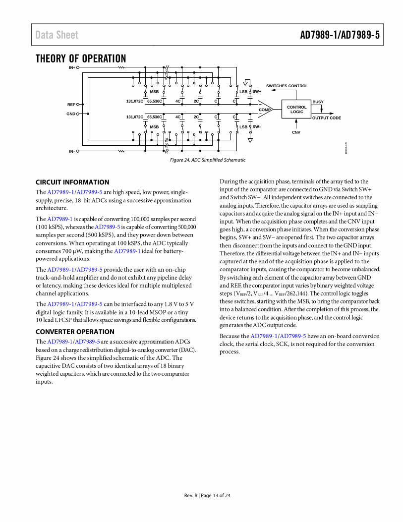
THEORY OF OPERATION
Figure 24. ADC Simplified Schematic
CIRCUIT INFORMATION The AD7989-1/AD7989-5 are high speed, low power, single-supply, precise, 18-bit ADCs using a successive approximation architecture.
The AD7989-1 is capable of converting 100,000 samples per second (100 kSPS), whereas the AD7989-5 is capable of converting 500,000 samples per second (500 kSPS), and they power down between conversions. When operating at 100 kSPS, the ADC typically consumes 700 µW, making the AD7989-1 ideal for battery-powered applications.
The AD7989-1/AD7989-5 provide the user with an on-chip track-and-hold amplifier and do not exhibit any pipeline delay or latency, making these devices ideal for multiple multiplexed channel applications.
The AD7989-1/AD7989-5 can be interfaced to any 1.8 V to 5 V digital logic family. It is available in a 10-lead MSOP or a tiny 10 lead LFCSP that allows space savings and flexible configurations.
CONVERTER OPERATION The AD7989-1/AD7989-5 are a successive approximation ADCs based on a charge redistribution digital-to-analog converter (DAC). Figure 24 shows the simplified schematic of the ADC. The capacitive DAC consists of two identical arrays of 18 binary weighted capacitors, which are connected to the two comparator inputs.
During the acquisition phase, terminals of the array tied to the input of the comparator are connected to GND via Switch SW+ and Switch SW−. All independent switches are connected to the analog inputs. Therefore, the capacitor arrays are used as sampling capacitors and acquire the analog signal on the IN+ input and IN− input. When the acquisition phase completes and the CNV input goes high, a conversion phase initiates. When the conversion phase begins, SW+ and SW− are opened first. The two capacitor arrays then disconnect from the inputs and connect to the GND input. Therefore, the differential voltage between the IN+ and IN− inputs captured at the end of the acquisition phase is applied to the comparator inputs, causing the comparator to become unbalanced. By switching each element of the capacitor array between GND and REF, the comparator input varies by binary weighted voltage steps (VREF/2, VREF/4 ... VREF/262,144). The control logic toggles these switches, starting with the MSB, to bring the comparator back into a balanced condition. After the completion of this process, the device returns to the acquisition phase, and the control logic generates the ADC output code.
Because the AD7989-1/AD7989-5 have an on-board conversion clock, the serial clock, SCK, is not required for the conversion process.
COMP CONTROLLOGIC
SWITCHES CONTROL
BUSY
OUTPUT CODE
CNV
CC2C65,536C 4C131,072C
LSB SW+MSB
LSB SW–MSB
CC2C65,536C 4C131,072C
IN+
REF
GND
IN– 1023
2-02
0
AD7989-1/AD7989-5 Data Sheet
Rev. B | Page 14 of 24
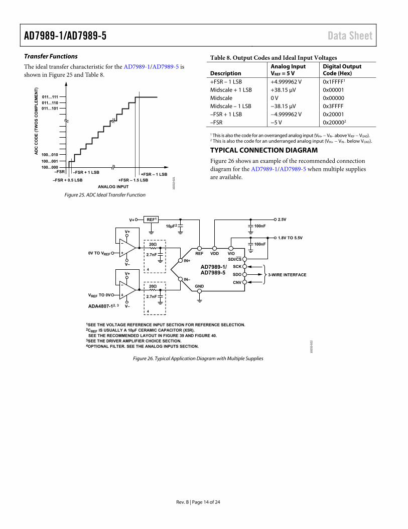
Transfer Functions
The ideal transfer characteristic for the AD7989-1/AD7989-5 is shown in Figure 25 and Table 8.
Figure 25. ADC Ideal Transfer Function
Table 8. Output Codes and Ideal Input Voltages
Description Analog Input VREF = 5 V
Digital Output Code (Hex)
+FSR – 1 LSB +4.999962 V 0x1FFFF1 Midscale + 1 LSB +38.15 μV 0x00001 Midscale 0 V 0x00000 Midscale – 1 LSB −38.15 μV 0x3FFFF –FSR + 1 LSB −4.999962 V 0x20001 –FSR −5 V 0x200002 1 This is also the code for an overranged analog input (VIN+ − VIN− above VREF − VGND). 2 This is also the code for an underranged analog input (VIN+ − VIN− below VGND).
TYPICAL CONNECTION DIAGRAM Figure 26 shows an example of the recommended connection diagram for the AD7989-1/AD7989-5 when multiple supplies are available.
Figure 26. Typical Application Diagram with Multiple Supplies
100...000
100...001
100...010
011...101011...110
011...111
AD
C C
OD
E (
TW
OS
CO
MP
LE
ME
NT
)
ANALOG INPUT
+FSR – 1.5 LSB
+FSR – 1 LSB–FSR + 1 LSB–FSR
–FSR + 0.5 LSB
1023
2-02
1
2.7nF
20Ω
V–
0V TO VREF
V+
4
2.7nF
20Ω
V–
VREF TO 0V
V+
4
10µF2
REF1
REF VDD VIO
GND
IN+
IN–
SCK
SDO
CNV
AD7989-1/AD7989-5
100nF
100nF
3-WIRE INTERFACE
2.5V
1.8V TO 5.5V
V+
ADA4807-12, 3
1SEE THE VOLTAGE REFERENCE INPUT SECTION FOR REFERENCE SELECTION.2CREF IS USUALLY A 10µF CERAMIC CAPACITOR (X5R).
SEE THE RECOMMENDED LAYOUT IN FIGURE 39 AND FIGURE 40.3SEE THE DRIVER AMPLIFIER CHOICE SECTION.4OPTIONAL FILTER. SEE THE ANALOG INPUTS SECTION.
SDI/CS
1023
2-02
2
Data Sheet AD7989-1/AD7989-5
Rev. B | Page 15 of 24
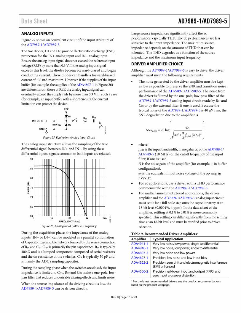
ANALOG INPUTS Figure 27 shows an equivalent circuit of the input structure of the AD7989-1/AD7989-5.
The two diodes, D1 and D2, provide electrostatic discharge (ESD) protection for the IN+ analog input and IN− analog input. Ensure the analog input signal does not exceed the reference input voltage (REF) by more than 0.3 V. If the analog input signal exceeds this level, the diodes become forward-biased and begin conducting current. These diodes can handle a forward-biased current of 130 mA maximum. However, if the supplies of the input buffer (for example, the supplies of the ADA4807-1 in Figure 26) are different from those of REF, the analog input signal can eventually exceed the supply rails by more than 0.3 V. In such a case (for example, an input buffer with a short circuit), the current limitation can protect the device.
Figure 27. Equivalent Analog Input Circuit
The analog input structure allows the sampling of the true differential signal between IN+ and IN−. By using these differential inputs, signals common to both inputs are rejected.
Figure 28. Analog Input CMRR vs. Frequency
During the acquisition phase, the impedance of the analog inputs (IN+ or IN−) can be modeled as a parallel combination of Capacitor CPIN and the network formed by the series connection of RIN and CIN. CPIN is primarily the pin capacitance. RIN is typically 400 Ω and is a lumped component composed of serial resistors and the on resistance of the switches. CIN is typically 30 pF and is mainly the ADC sampling capacitor.
During the sampling phase when the switches are closed, the input impedance is limited to CPIN. RIN and CIN make a one-pole, low-pass filter that reduces undesirable aliasing effects and limits noise.
When the source impedance of the driving circuit is low, the AD7989-1/AD7989-5 can be driven directly.
Large source impedances significantly affect the ac performance, especially THD. The dc performances are less sensitive to the input impedance. The maximum source impedance depends on the amount of THD that can be tolerated. The THD degrades as a function of the source impedance and the maximum input frequency.
DRIVER AMPLIFIER CHOICE Although the AD7989-1/AD7989-5 is easy to drive, the driver amplifier must meet the following requirements:
The noise generated by the driver amplifier must be kept as low as possible to preserve the SNR and transition noise performance of the AD7989-1/AD7989-5. The noise from the driver is filtered by the one-pole, low-pass filter of the AD7989-1/AD7989-5 analog input circuit made by RIN and CIN or by the external filter, if one is used. Because the typical noise of the AD7989-1/AD7989-5 is 40 μV rms, the SNR degradation due to the amplifier is
22 )(
2π
40
40log20
N3dB
LOSS
NefSNR
where: f–3dB is the input bandwidth, in megahertz, of the AD7989-1/ AD7989-5 (10 MHz) or the cutoff frequency of the input filter, if one is used. N is the noise gain of the amplifier (for example, 1 in buffer configuration). eN is the equivalent input noise voltage of the op amp in nV/√Hz.
For ac applications, use a driver with a THD performance commensurate with the AD7989-1/AD7989-5.
For multichannel, multiplexed applications, the driver amplifier and the AD7989-1/AD7989-5 analog input circuit must settle for a full-scale step onto the capacitor array at an 18-bit level (0.0004%, 4 ppm). In the data sheet of the amplifier, settling at 0.1% to 0.01% is more commonly specified. This settling can differ significantly from the settling time at an 18-bit level and must be verified prior to driver selection.
Table 9. Recommended Driver Amplifiers1 Amplifier Typical Application ADA4941-1 Very low noise, low power, single to differentialADA4940-1 Very low noise, low power, single to differential ADA4807-2 Very low noise and low power ADA4627-1 Precision, low noise and low input bias ADA4522-2 Precision, zero drift and electromagnetic interference
(EMI) enhanced ADA4500-2 Precision, rail-to-rail input and output (RRIO) and
zero input crossover distortion 1 For the latest recommended drivers, see the product recommendations listed on the product webpage.
CPIN
REF
RINCIN
D1
D2
IN+ OR IN–
GND
1023
2-02
3
90
85
80
75
70
65
601 10 100 1k 10k
FREQUENCY (kHz)
CM
RR
(d
B)
1023
2-02
4
AD7989-1/AD7989-5 Data Sheet
Rev. B | Page 16 of 24
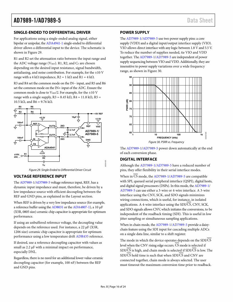
SINGLE-ENDED TO DIFFERENTIAL DRIVER For applications using a single-ended analog signal, either bipolar or unipolar, the ADA4941-1 single-ended to differential driver allows a differential input to the device. The schematic is shown in Figure 29.
R1 and R2 set the attenuation ratio between the input range and the ADC voltage range (VREF). R1, R2, and CF are chosen depending on the desired input resistance, signal bandwidth, antialiasing, and noise contribution. For example, for the ±10 V range with a 4 kΩ impedance, R2 = 1 kΩ and R1 = 4 kΩ.
R3 and R4 set the common mode on the IN− input, and R5 and R6 set the common mode on the IN+ input of the ADC. Ensure the common mode is close to VREF/2. For example, for the ±10 V range with a single supply, R3 = 8.45 kΩ, R4 = 11.8 kΩ, R5 = 10.5 kΩ, and R6 = 9.76 kΩ.
Figure 29. Single-Ended to Differential Driver Circuit
VOLTAGE REFERENCE INPUT The AD7989-1/AD7989-5 voltage reference input, REF, has a dynamic input impedance and must, therefore, be driven by a low impedance source with efficient decoupling between the REF and GND pins, as explained in the Layout section.
When REF is driven by a very low impedance source (for example, a reference buffer using the AD8031 or the ADA4807-1), a 10 μF (X5R, 0805 size) ceramic chip capacitor is appropriate for optimum performance.
If using an unbuffered reference voltage, the decoupling value depends on the reference used. For instance, a 22 μF (X5R, 1206 size) ceramic chip capacitor is appropriate for optimum performance using a low temperature drift ADR435 reference.
If desired, use a reference decoupling capacitor with values as small as 2.2 μF with a minimal impact on performance, especially DNL.
Regardless, there is no need for an additional lower value ceramic decoupling capacitor (for example, 100 nF) between the REF and GND pins.
POWER SUPPLY The AD7989-1/AD7989-5 use two power supply pins: a core supply (VDD) and a digital input/output interface supply (VIO). VIO allows direct interface with any logic between 1.8 V and 5.5 V. To reduce the number of supplies needed, tie VIO and VDD together. The AD7989-1/AD7989-5 are independent of power supply sequencing between VIO and VDD. Additionally, they are insensitive to power supply variations over a wide frequency range, as shown in Figure 30.
Figure 30. PSRR vs. Frequency
The AD7989-1/AD7989-5 power down automatically at the end of each conversion phase.
DIGITAL INTERFACE Although the AD7989-1/AD7989-5 have a reduced number of pins, they offer flexibility in their serial interface modes.
When in CS mode, the AD7989-1/AD7989-5 are compatible with SPI, queued serial peripheral interface (QSPI), digital hosts, and digital signal processors (DSPs). In this mode, the AD7989-1/ AD7989-5 can use either a 3-wire or 4-wire interface. A 3-wire interface using the CNV, SCK, and SDO signals minimizes wiring connections, which is useful, for instance, in isolated applications. A 4-wire interface using the SDI/CS, CNV, SCK, and SDO signals allows CNV, which initiates the conversions, to be independent of the readback timing (SDI). This is useful in low jitter sampling or simultaneous sampling applications.
When in chain mode, the AD7989-1/AD7989-5 provide a daisy-chain feature using the SDI input for cascading multiple ADCs on a single data line, similar to a shift register.
The mode in which the device operates depends on the SDI/CS level when the CNV rising edge occurs. CS mode is selected if SDI/CS is high, and chain mode is selected if SDI/CS is low. The SDI/CS hold time is such that when SDI/CS and CNV are connected together, chain mode is always selected. The user must timeout the maximum conversion time prior to readback.
20Ω
20Ω
10µF
R1
100nF
+2.5V
+5V REF
+5.2V
–0.2V
CF
R2
R4
R6
±10V,±5V, ..
R3
R5
REF VDD
GND
IN+
IN–
AD7989-1/AD7989-52.7nF
2.7nF
ADA4941
IN
FB
OUTP
OUTNREF
100nF
1023
2-02
5
95
90
85
80
75
70
65
60
PS
RR
(d
B)
1 10 100 1kFREQUENCY (kHz) 10
232-
026
Data Sheet AD7989-1/AD7989-5
Rev. B | Page 17 of 24
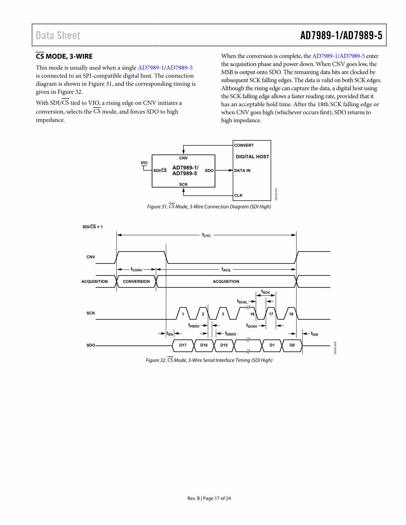
CS MODE, 3-WIRE
This mode is usually used when a single AD7989-1/AD7989-5 is connected to an SPI-compatible digital host. The connection diagram is shown in Figure 31, and the corresponding timing is given in Figure 32.
With SDI/CS tied to VIO, a rising edge on CNV initiates a conversion, selects the CS mode, and forces SDO to high impedance.
When the conversion is complete, the AD7989-1/AD7989-5 enter the acquisition phase and power down. When CNV goes low, the MSB is output onto SDO. The remaining data bits are clocked by subsequent SCK falling edges. The data is valid on both SCK edges. Although the rising edge can capture the data, a digital host using the SCK falling edge allows a faster reading rate, provided that it has an acceptable hold time. After the 18th SCK falling edge or when CNV goes high (whichever occurs first), SDO returns to high impedance.
Figure 31. CS Mode, 3-Wire Connection Diagram (SDI High)
Figure 32. CS Mode, 3-Wire Serial Interface Timing (SDI High)
AD7989-1/AD7989-5
SDO
CNV
SCK
CONVERT
DATA IN
CLK
DIGITAL HOSTVIO
SDI/CS
1023
2-02
7
SDO D17 D16 D15 D1 D0
tDIS
SCK 1 2 3 16 17 18
tSCK
tSCKL
tSCKHtHSDO
tDSDO
CNV
CONVERSIONACQUISITION
tCONV
tCYC
ACQUISITION
tACQ
tEN
SDI/CS = 1
1023
2-02
8
AD7989-1/AD7989-5 Data Sheet
Rev. B | Page 18 of 24
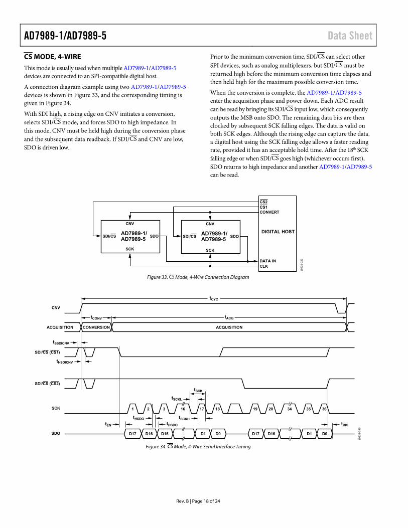
CS MODE, 4-WIRE
This mode is usually used when multiple AD7989-1/AD7989-5 devices are connected to an SPI-compatible digital host.
A connection diagram example using two AD7989-1/AD7989-5 devices is shown in Figure 33, and the corresponding timing is given in Figure 34.
With SDI high, a rising edge on CNV initiates a conversion, selects SDI/CS mode, and forces SDO to high impedance. In this mode, CNV must be held high during the conversion phase and the subsequent data readback. If SDI/CS and CNV are low, SDO is driven low.
Prior to the minimum conversion time, SDI/CS can select other SPI devices, such as analog multiplexers, but SDI/CS must be returned high before the minimum conversion time elapses and then held high for the maximum possible conversion time.
When the conversion is complete, the AD7989-1/AD7989-5 enter the acquisition phase and power down. Each ADC result can be read by bringing its SDI/CS input low, which consequently outputs the MSB onto SDO. The remaining data bits are then clocked by subsequent SCK falling edges. The data is valid on both SCK edges. Although the rising edge can capture the data, a digital host using the SCK falling edge allows a faster reading rate, provided it has an acceptable hold time. After the 18th SCK falling edge or when SDI/CS goes high (whichever occurs first), SDO returns to high impedance and another AD7989-1/AD7989-5 can be read.
Figure 33. CS Mode, 4-Wire Connection Diagram
Figure 34. CS Mode, 4-Wire Serial Interface Timing
AD7989-1/AD7989-5
SDO
CNV
SCK
CONVERT
DATA INCLK
DIGITAL HOST
CS1CS2
AD7989-1/AD7989-5
SDO
CNV
SCK
SDI/CS SDI/CS
1023
2-02
9
SDO D17 D16 D15 D1 D0
tDIS
SCK 1 2 3 34 35 36
tHSDO
tDSDOtEN
CONVERSIONACQUISITION
tCONV
tCYC
tACQ
ACQUISITION
CNV
tSSDICNV
tHSDICNV
D1
16 17
tSCK
tSCKL
tSCKH
D0 D17 D16
19 2018
SDI/CS (CS1)
SDI/CS (CS2)
1023
2-03
0
Data Sheet AD7989-1/AD7989-5
Rev. B | Page 19 of 24
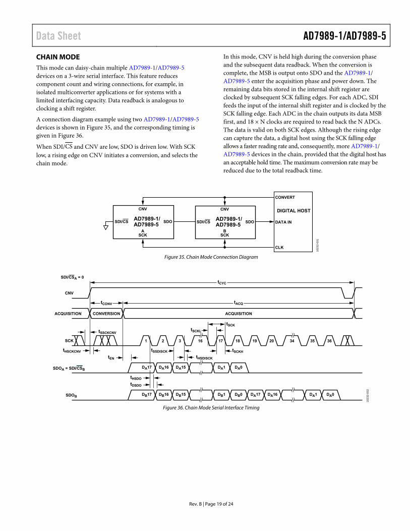
CHAIN MODE This mode can daisy-chain multiple AD7989-1/AD7989-5 devices on a 3-wire serial interface. This feature reduces component count and wiring connections, for example, in isolated multiconverter applications or for systems with a limited interfacing capacity. Data readback is analogous to clocking a shift register.
A connection diagram example using two AD7989-1/AD7989-5 devices is shown in Figure 35, and the corresponding timing is given in Figure 36.
When SDI/CS and CNV are low, SDO is driven low. With SCK low, a rising edge on CNV initiates a conversion, and selects the chain mode.
In this mode, CNV is held high during the conversion phase and the subsequent data readback. When the conversion is complete, the MSB is output onto SDO and the AD7989-1/ AD7989-5 enter the acquisition phase and power down. The remaining data bits stored in the internal shift register are clocked by subsequent SCK falling edges. For each ADC, SDI feeds the input of the internal shift register and is clocked by the SCK falling edge. Each ADC in the chain outputs its data MSB first, and 18 × N clocks are required to read back the N ADCs. The data is valid on both SCK edges. Although the rising edge can capture the data, a digital host using the SCK falling edge allows a faster reading rate and, consequently, more AD7989-1/ AD7989-5 devices in the chain, provided that the digital host has an acceptable hold time. The maximum conversion rate may be reduced due to the total readback time.
Figure 35. Chain Mode Connection Diagram
Figure 36. Chain Mode Serial Interface Timing
CONVERT
DATA IN
CLK
DIGITAL HOST
AD7989-1/AD7989-5
SDO
CNV
BSCK
AD7989-1/AD7989-5
SDO
CNV
ASCK
SDI/CS SDI/CS
1023
2-03
1
DA17 DA16 DA15
SCK 1 2 3 34 35 36
tSSDISCK
tHSDISCKtEN
CONVERSIONACQUISITION
tCONV
tCYC
tACQ
ACQUISITION
CNV
DA1
16 17
tSCK
tSCKL
tSCKH
DA0
19 2018
SDOB DB17 DB16 DB15 DA1DB1 DB0 DA17 DA16
tHSDO
tDSDO
tSSCKCNV
tHSCKCNV
DA0
SDI/CSA = 0
SDOA = SDI/CSB10
232-
032
AD7989-1/AD7989-5 Data Sheet
Rev. B | Page 20 of 24
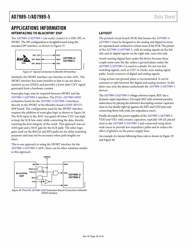
APPLICATIONS INFORMATION INTERFACING TO BLACKFIN® DSP The AD7989-1/AD7989-5 can easily connect to a DSP, SPI, or SPORT. The SPI configuration is straightforward using the standard SPI interface, as shown in Figure 37.
Figure 37. Typical Connection to Blackfin SPI Interface
Similarly, the SPORT interface can interface to this ADC. The SPORT interface has some benefits in that it can use direct memory access (DMA) and provides a lower jitter CNV signal generated from a hardware counter.
Some glue logic may be required between SPORT and the AD7989-1/AD7989-5 interface. The EVAL-AD7989-5SDZ evaluation board for the AD7989-1/AD7989-5 interfaces directly to the SPORT of the Blackfin-based (ADSP-BF527) SDP board. The configuration used for the SPORT interface requires the addition of some glue logic as shown in Figure 38. The SCK input to the ADC was gated off when CNV was high to keep the SCK line static while converting the data, thereby ensuring the best integrity of the result. This approach uses an AND gate and a NOT gate for the SCK path. The other logic gates used on the RSCLK and RFS paths are for delay matching purposes and may not be necessary when path lengths are short.
This is one approach to using the SPORT interface for the AD7989-1/AD7989-5 ADC; there can be other solutions similar to this approach.
Figure 38. The EVAL-AD7989-5SDZ Evaluation Board Connection to Blackfin
SPORT Interface
LAYOUT The printed circuit board (PCB) that houses the AD7989-1/ AD7989-5 must be designed so the analog and digital sections are separated and confined to certain areas of the PCB. The pinout of the AD7989-1/AD7989-5, with its analog signals on the left side and its digital signals on the right side, eases this task.
Avoid running digital lines under the device because these couple noise onto the die, unless a ground plane under the AD7989-1/AD7989-5 is used as a shield. Do not run fast switching signals, such as CNV or clocks, near analog signal paths. Avoid crossover of digital and analog signals.
Using at least one ground plane is recommended. It can be common or split between the digital and analog sections. In the latter case, join the planes underneath the AD7989-1/AD7989-5 devices.
The AD7989-1/AD7989-5 voltage reference input, REF, has a dynamic input impedance. Decouple REF with minimal parasitic inductances by placing the reference decoupling ceramic capacitor close to, but ideally right up against, the REF and GND pins and connecting them with wide, low impedance traces.
Finally, decouple the power supplies of the AD7989-1/AD7989-5, VDD and VIO, with ceramic capacitors, typically 100 nF, placed close to the AD7989-1/AD7989-5 and connected using short, wide traces to provide low impedance paths and to reduce the effect of glitches on the power supply lines.
An example of a layout following these rules is shown in Figure 39 and Figure 40.
AD7989-1/AD7989-5
SCK
SDO
CNV
SPI_CLK
SPI_MISO
SPI_MOSI
1023
2-03
5DSP
SCK
SDO
CNV
TSCLK
DR
TFS
RFS
RSCLK
VDRIVE
AD7989-1/AD7989-5
1023
2-04
5
BLACKFINDSP
Data Sheet AD7989-1/AD7989-5
Rev. B | Page 21 of 24
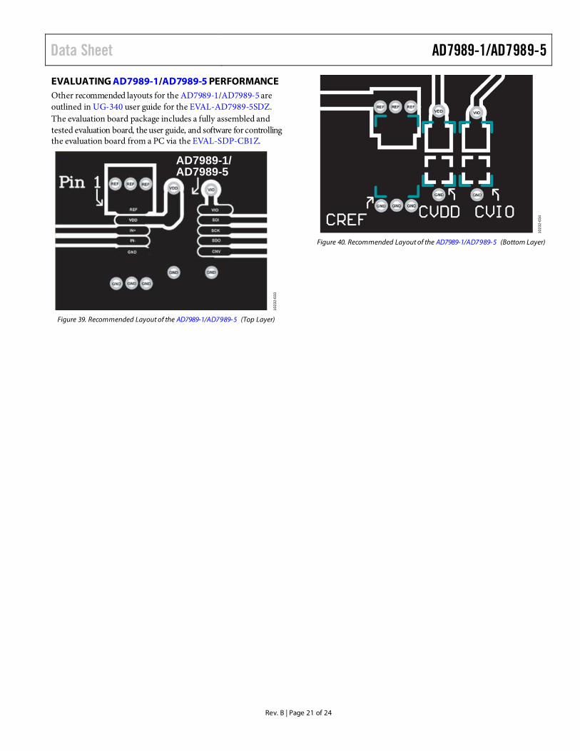
EVALUATING AD7989-1/AD7989-5 PERFORMANCE Other recommended layouts for the AD7989-1/AD7989-5 are outlined in UG-340 user guide for the EVAL-AD7989-5SDZ. The evaluation board package includes a fully assembled and tested evaluation board, the user guide, and software for controlling the evaluation board from a PC via the EVAL-SDP-CB1Z.
Figure 39. Recommended Layout of the AD7989-1/AD7989-5 (Top Layer)
Figure 40. Recommended Layout of the AD7989-1/AD7989-5 (Bottom Layer)
AD7989-1/AD7989-5
1023
2-03
3
1023
2-03
4
AD7989-1/AD7989-5 Data Sheet
Rev. B | Page 22 of 24
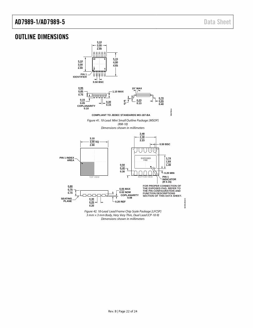
OUTLINE DIMENSIONS
Figure 41. 10-Lead Mini Small Outline Package [MSOP]
(RM-10) Dimensions shown in millimeters
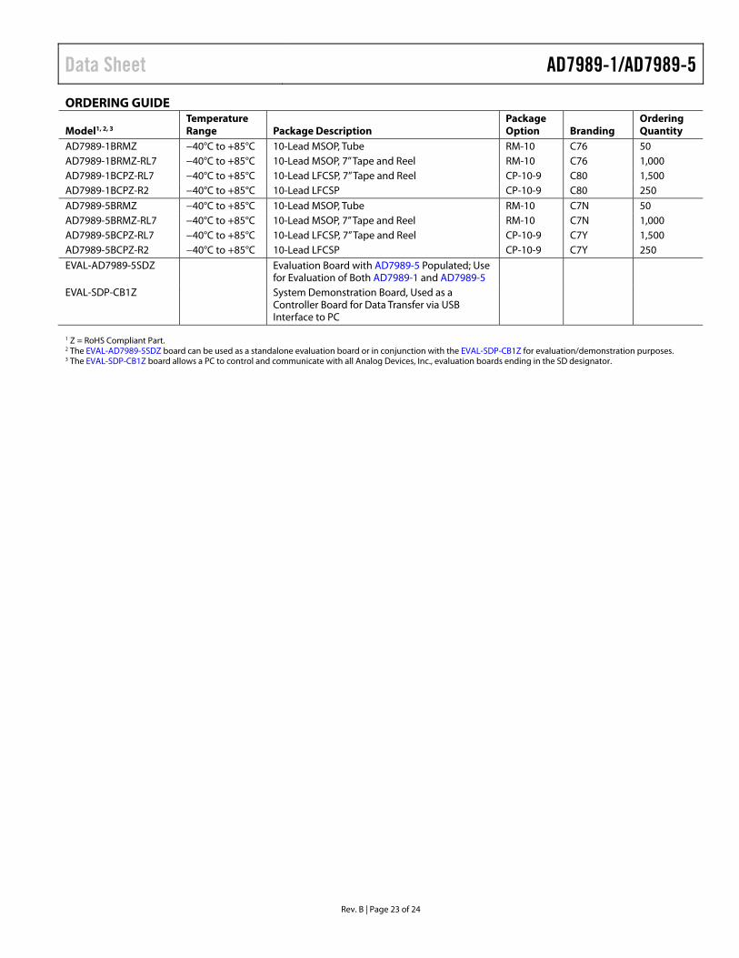
Figure 42. 10-Lead Lead Frame Chip Scale Package [LFCSP]
3 mm × 3 mm Body, Very Very Thin, Dual Lead (CP-10-9) Dimensions shown in millimeters
COMPLIANT TO JEDEC STANDARDS MO-187-BA 0917
09-A
6°0°
0.700.550.40
5
10
1
6
0.50 BSC
0.300.15
1.10 MAX
3.103.002.90
COPLANARITY0.10
0.230.13
3.103.002.90
5.154.904.65
PIN 1IDENTIFIER
15° MAX0.950.850.75
0.150.05
2.482.382.23
0.500.400.30
10
1
6
5
0.300.250.20
PIN 1 INDEXAREA
SEATINGPLANE
0.800.750.70
1.741.641.49
0.20 REF
0.05 MAX0.02 NOM
0.50 BSC
EXPOSEDPAD
3.103.00 SQ2.90
PIN 1INDICATOR(R 0.15)
FOR PROPER CONNECTION OFTHE EXPOSED PAD, REFER TOTHE PIN CONFIGURATION ANDFUNCTION DESCRIPTIONSSECTION OF THIS DATA SHEET.COPLANARITY
0.08
02-0
5-20
13-C
TOP VIEW BOTTOM VIEW
0.20 MIN
Data Sheet AD7989-1/AD7989-5
Rev. B | Page 23 of 24
ORDERING GUIDE
Model1, 2, 3 Temperature Range Package Description
Package Option Branding
Ordering Quantity
AD7989-1BRMZ −40°C to +85°C 10-Lead MSOP, Tube RM-10 C76 50 AD7989-1BRMZ-RL7 −40°C to +85°C 10-Lead MSOP, 7” Tape and Reel RM-10 C76 1,000 AD7989-1BCPZ-RL7 −40°C to +85°C 10-Lead LFCSP, 7” Tape and Reel CP-10-9 C80 1,500 AD7989-1BCPZ-R2 −40°C to +85°C 10-Lead LFCSP CP-10-9 C80 250 AD7989-5BRMZ −40°C to +85°C 10-Lead MSOP, Tube RM-10 C7N 50 AD7989-5BRMZ-RL7 −40°C to +85°C 10-Lead MSOP, 7” Tape and Reel RM-10 C7N 1,000 AD7989-5BCPZ-RL7 −40°C to +85°C 10-Lead LFCSP, 7” Tape and Reel CP-10-9 C7Y 1,500 AD7989-5BCPZ-R2 −40°C to +85°C 10-Lead LFCSP CP-10-9 C7Y 250 EVAL-AD7989-5SDZ Evaluation Board with AD7989-5 Populated; Use
for Evaluation of Both AD7989-1 and AD7989-5
EVAL-SDP-CB1Z System Demonstration Board, Used as a Controller Board for Data Transfer via USB Interface to PC
1 Z = RoHS Compliant Part. 2 The EVAL-AD7989-5SDZ board can be used as a standalone evaluation board or in conjunction with the EVAL-SDP-CB1Z for evaluation/demonstration purposes. 3 The EVAL-SDP-CB1Z board allows a PC to control and communicate with all Analog Devices, Inc., evaluation boards ending in the SD designator.
AD7989-1/AD7989-5 Data Sheet
Rev. B | Page 24 of 24
NOTES
©2014–2017 Analog Devices, Inc. All rights reserved. Trademarks and registered trademarks are the property of their respective owners. D10232-0-1/17(B)