Embed Size (px)
DESCRIPTION
ADAIC
Citation preview

ANALYSIS AND DESIGN OF ANALOG INTEGRATED CIRCUITS
UNIT 1SINGLE STAGE AMPLIFIERS

Single-Transistor Amplifier Stages
• Bipolar and MOS transistors are capable of providing useful amplification in three different configurations. In the common-emitter or common-source configuration, the signal is applied to the base or gate of the transistor and the amplified output is taken from the collector or drain.
• In the common-collector or common-drain configuration, the signal is applied to the base or gate and the output signal is taken from the emitter or source. This configuration is often referred to as the emitter follower for bipolar circuits and the source follower for MOS circuits.
• In the common-base or common-gate configuration, the signal is applied to the emitter or the source, and the output signal is taken from the collector or the drain. Each of these configurations provides a unique combination of input resistance, output resistance, voltage gain, and current gain. In many instances, the analysis of complex multistage amplifiers can be reduced to the analysis of a number of single-transistor stages of these types.


Common-Source Configuration
• The resistively loaded common-source (CS) amplifier configuration is shown in Fig. 3.12a using an-channel MOS transistor. The corresponding small-signal equivalent circuit is shown in Fig. 3.12b.
• As in the case of the bipolar transistor, the MOS transistor is cutoff for Vi =0 and thus Id=0 and Vo=VDD. AsVi is increased beyond the threshold voltage Vt, nonzero drain current flows and the transistor operates in the active region (which is often called saturation for MOS transistors) when Vo>VGS−Vt.

Common-Source Configuration

• The output voltage is equal to the drain-source voltage and decreases as the input increases. When Vo<VGS−Vt , the transistor enters the triode region, where its output resistance becomes low and the small-signal voltage gain drops dramatically.
Common-Source Configuration


Common-Drain Configuration (Source Follower)
• The common-drain configuration is shown in Fig. 3.25a. The input signal is applied to the gate and the output is taken from the source. From a large-signal standpoint, the output voltage is equal to the input voltage minus the gate-source voltage.
• The gate-source voltage consists of two parts: – the threshold – the overdrive.

Common-Drain Configuration (Source Follower)


Common-Drain Configuration (Source Follower)

Common-Drain Configuration (Source Follower)

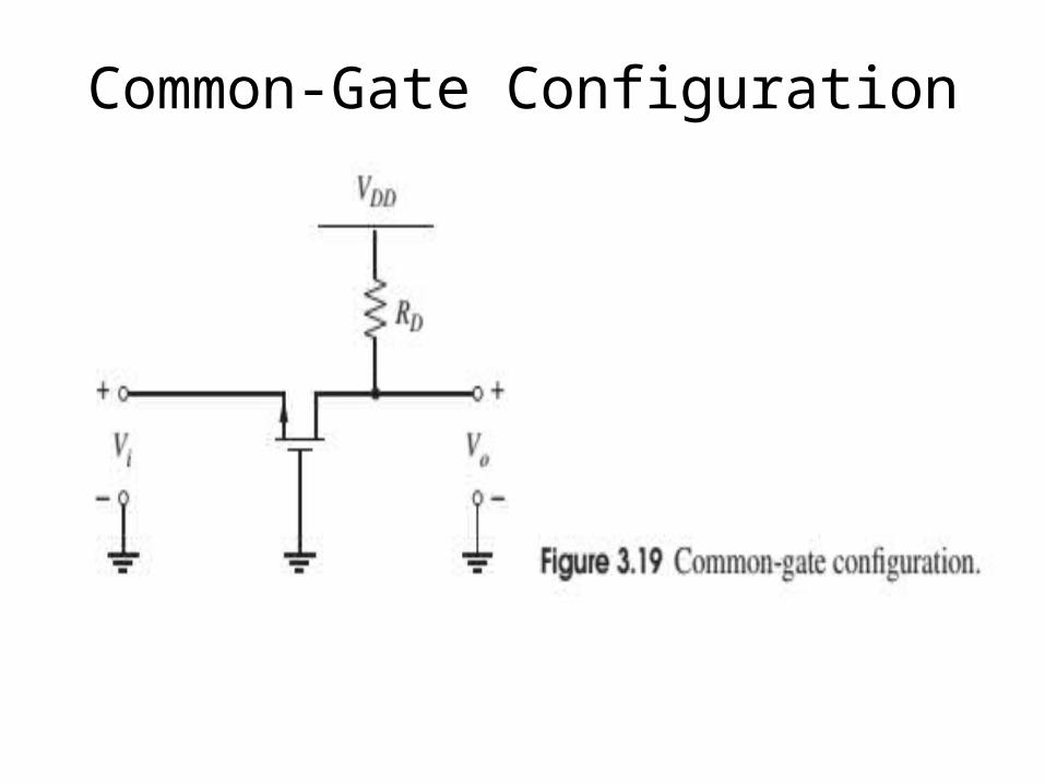
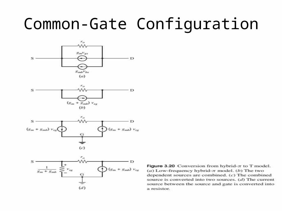
Common-Gate Configuration• In the common-gate configuration, the input signal is applied to
the source of the transistor, and the output is taken from the drain while the gate is connected to ac ground. This configuration is shown in Fig. 3.19, and its behavior is similar to that of a common-base stage.
• The analysis of common gate amplifiers can be simplified if the model is changed from a hybrid-πconfiguration to a T model, as shown in Fig. 3.20. In Fig. 3.20a, the low-frequency hybrid-πmodel is shown.
• Note that both trans conductance generators are now active. If the substrate or body connection is assumed to operate at ac ground, then vbs=vgs because the gate also operates at ac ground.


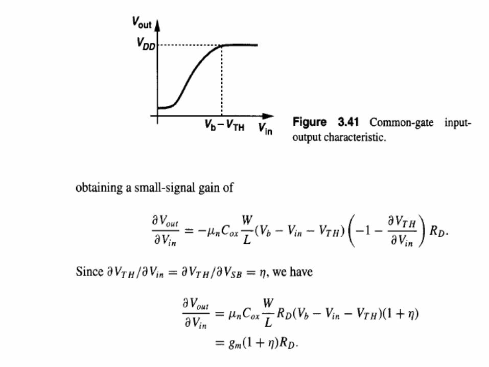


Common-Gate Configuration
Common-Gate Configuration

Common-Gate Configuration

Cascode Configuration• The cascode configuration was first invented for vacuum-tube
circuits. The terminal that emits electrons is the cathode, the terminal that controls current flow is the grid, and the terminal that collects electrons is the anode.
• The cascode is a cascade of common cathode and common-grid stages joined at the anode of the first stage and the cathode of the second stage. The cascode configuration is important mostly because it increases output resistance and reduces unwanted capacitive feedback in amplifiers, allowing operation at higher frequencies than would otherwise be possible.
• The high output resistance attainable is particularly useful in desensitizing bias references from variations in power-supply voltage and in achieving large amounts of voltage gain.

Bipolar Cascode
• In bipolar form, the cascode is a common-emitter–common-base (CE-CB) amplifier, as shown in Fig. 3.36. We will assume here that rb in both devices is zero.
• Although the base resistances have a negligible effect on the low-frequency performance, the effects of non zero rb are important in the high-frequency performance of this combination.

Bipolar Cascode


Bipolar Cascode
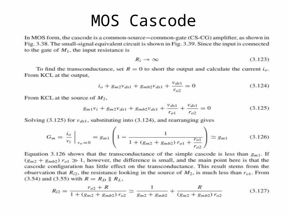
MOS Cascode

MOS Cascode

MOS Cascode

MOS Cascode


![Unit 1 Unit 2 Unit 3 Unit 4 Unit 5 Unit 6 Unit 7 Unit 8 ... 5 - Formatted.pdf · Unit 1 Unit 2 Unit 3 Unit 4 Unit 5 Unit 6 ... and Scatterplots] Unit 5 – Inequalities and Scatterplots](https://img.pdfslide.net/doc/110x75/5b76ea0a7f8b9a4c438c05a9/unit-1-unit-2-unit-3-unit-4-unit-5-unit-6-unit-7-unit-8-5-formattedpdf.jpg)