Embed Size (px)
DESCRIPTION
ADAIC
Citation preview

ANALYSIS AND DESIGN OF ANALOG INTEGRATED CIRCUITS
UNIT 1SINGLE STAGE AMPLIFIERS

Single-Transistor Amplifier Stages
• Bipolar and MOS transistors are capable of providing useful amplification in three different configurations. In the common-emitter or common-source configuration, the signal is applied to the base or gate of the transistor and the amplified output is taken from the collector or drain.
• In the common-collector or common-drain configuration, the signal is applied to the base or gate and the output signal is taken from the emitter or source. This configuration is often referred to as the emitter follower for bipolar circuits and the source follower for MOS circuits.
• In the common-base or common-gate configuration, the signal is applied to the emitter or the source, and the output signal is taken from the collector or the drain. Each of these configurations provides a unique combination of input resistance, output resistance, voltage gain, and current gain. In many instances, the analysis of complex multistage amplifiers can be reduced to the analysis of a number of single-transistor stages of these types.

Common-Source Configuration
• The resistively loaded common-source (CS) amplifier configuration is shown in Fig. 3.12a using an-channel MOS transistor. The corresponding small-signal equivalent circuit is shown in Fig. 3.12b.
• As in the case of the bipolar transistor, the MOS transistor is cutoff for Vi =0 and thus Id=0 and Vo=VDD. AsVi is increased beyond the threshold voltage Vt, nonzero drain current flows and the transistor operates in the active region (which is often called saturation for MOS transistors) when Vo>VGS−Vt.
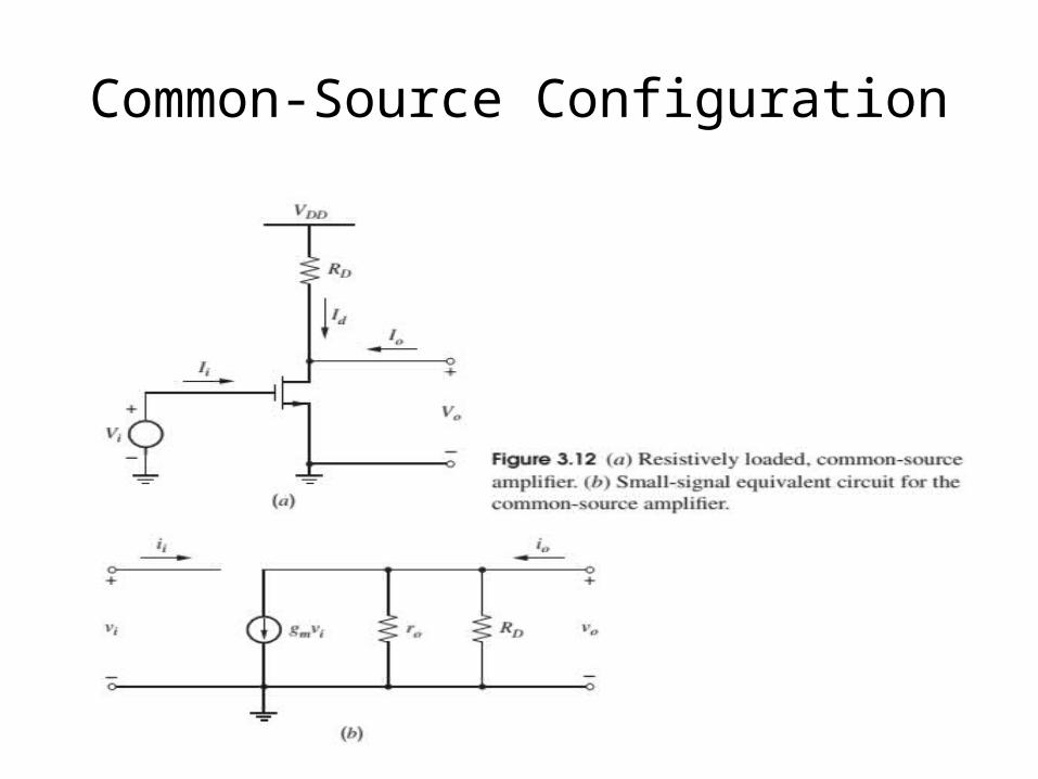
Common-Source Configuration

• The output voltage is equal to the drain-source voltage and decreases as the input increases. When Vo<VGS−Vt , the transistor enters the triode region, where its output resistance becomes low and the small-signal voltage gain drops dramatically.
Common-Source Configuration
Common-Drain Configuration (Source Follower)
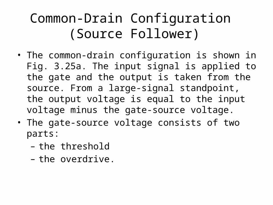
• The common-drain configuration is shown in Fig. 3.25a. The input signal is applied to the gate and the output is taken from the source. From a large-signal standpoint, the output voltage is equal to the input voltage minus the gate-source voltage.
• The gate-source voltage consists of two parts: – the threshold – the overdrive.

Common-Drain Configuration (Source Follower)

Common-Drain Configuration (Source Follower)

Common-Drain Configuration (Source Follower)

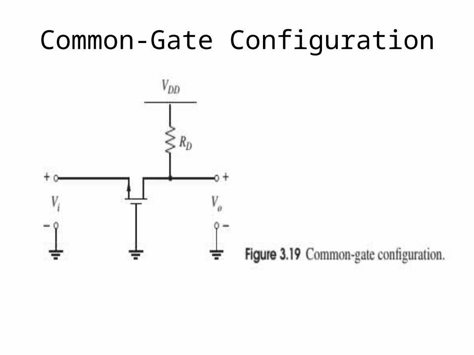
Common-Gate Configuration• In the common-gate configuration, the input signal is applied to
the source of the transistor, and the output is taken from the drain while the gate is connected to ac ground. This configuration is shown in Fig. 3.19, and its behavior is similar to that of a common-base stage.
• The analysis of common gate amplifiers can be simplified if the model is changed from a hybrid-πconfiguration to a T model, as shown in Fig. 3.20. In Fig. 3.20a, the low-frequency hybrid-πmodel is shown.
• Note that both trans conductance generators are now active. If the substrate or body connection is assumed to operate at ac ground, then vbs=vgs because the gate also operates at ac ground.
Common-Gate Configuration

Common-Gate Configuration

Common-Gate Configuration

Cascode Configuration• The cascode configuration was first invented for vacuum-tube
circuits. The terminal that emits electrons is the cathode, the terminal that controls current flow is the grid, and the terminal that collects electrons is the anode.
• The cascode is a cascade of common cathode and common-grid stages joined at the anode of the first stage and the cathode of the second stage. The cascode configuration is important mostly because it increases output resistance and reduces unwanted capacitive feedback in amplifiers, allowing operation at higher frequencies than would otherwise be possible.
• The high output resistance attainable is particularly useful in desensitizing bias references from variations in power-supply voltage and in achieving large amounts of voltage gain.

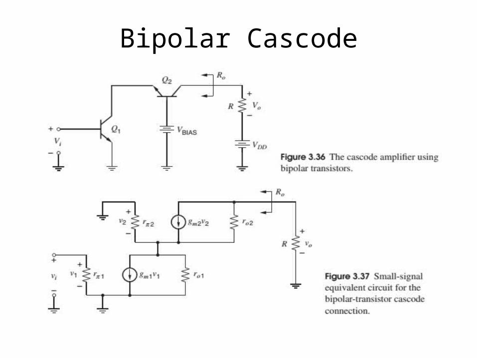
Bipolar Cascode
• In bipolar form, the cascode is a common-emitter–common-base (CE-CB) amplifier, as shown in Fig. 3.36. We will assume here that rb in both devices is zero.
• Although the base resistances have a negligible effect on the low-frequency performance, the effects of non zero rb are important in the high-frequency performance of this combination.
Bipolar Cascode

Bipolar Cascode

Bipolar Cascode
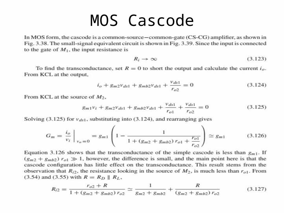
MOS Cascode

MOS Cascode
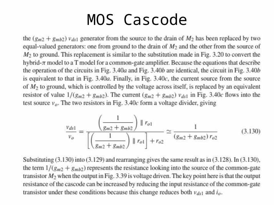
MOS Cascode
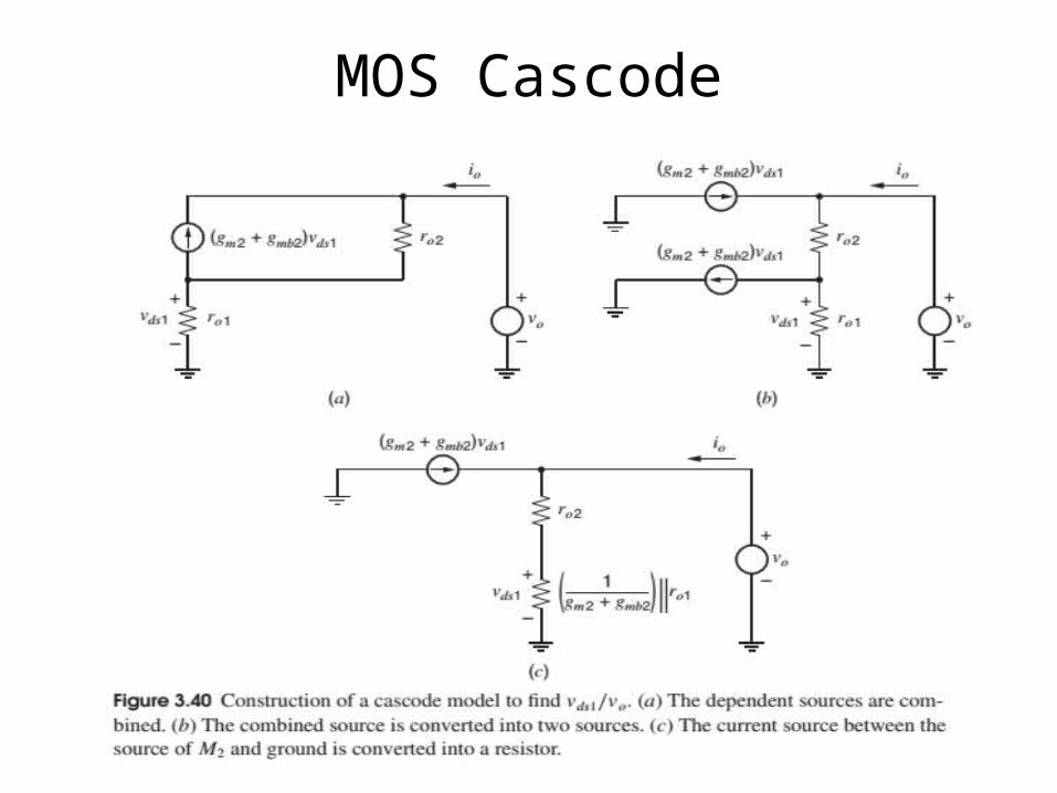
MOS Cascode
Differential Pairs
• The differential pair is another example of a circuit that was first invented for use with vacuum tubes. The original circuit uses two vacuum tubes whose cathodes are connected together.
• Modern differential pairs use bipolar or MOS transistors coupled at their emitters or sources, respectively, and are perhaps the most widely used two-transistor sub circuits in monolithic analog circuits.
• The usefulness of the differential pair stems from two key properties. – First, cascades of differential pairs can be directly connected to
one another without inter stage coupling capacitors. – Second, the differential pair is primarily sensitive to the
difference between two input voltages, allowing a high degree of rejection of signals common to both inputs.
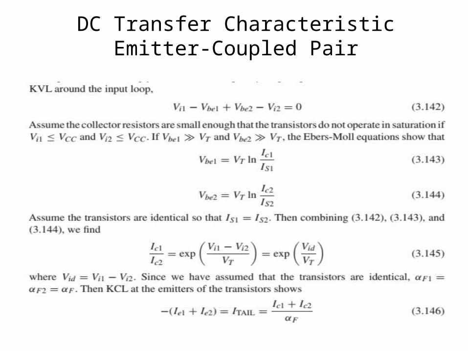
DC Transfer Characteristic Emitter-Coupled Pair
• The simplest form of an emitter-coupled pair is shown in Fig. 3.45. The biasing circuit in the lead connected to the emitters of Q1 and Q2 can be a transistor current source, which is called a tail current source, or a simple resistor.
• If a simple resistor RTAIL is used alone, ITAIL=0 in Fig. 3.45. Otherwise , ITAIL and RTAIL together form a Norton-equivalent model of the tail current source.
• The large-signal behavior of the emitter-coupled pair is important in part because it illustrates the limited range of input voltages over which the circuit behaves almost linearly.

• The large-signal behavior shows that the amplitude of analog signals in bipolar circuits can be limited without pushing the transistors into saturation, where the response time would be increased because of excess charge storage in the base region.
• For simplicity in the analysis, we assume that the output resistance of the tail current source – RTAIL→∞
• The output resistance of each transistor– ro→∞
• The base resistance of each transistor rb=0.
DC Transfer Characteristic Emitter-Coupled Pair

DC Transfer Characteristic Emitter-Coupled Pair
DC Transfer Characteristic Emitter-Coupled Pair

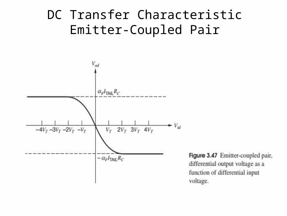
These two currents are shown as a function of Vid in Fig. 3.46. When the magnitude of Vid is greater than about 3VT, which is approximately 78 mV at room temperature, the collector currents are almost independent of Vid because one of the transistors turns off and the other conducts all the current that flows.
DC Transfer Characteristic Emitter-Coupled Pair

DC Transfer Characteristic Emitter-Coupled Pair
DC Transfer Characteristic Emitter-Coupled Pair

DC Transfer Characteristic Emitter-Coupled Pair
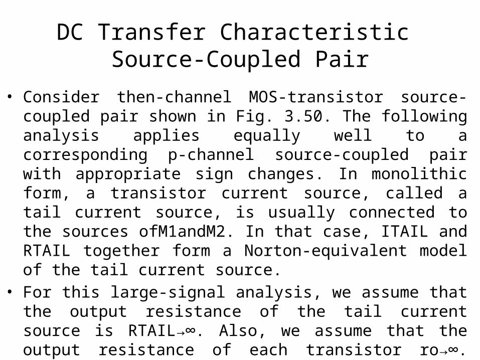
DC Transfer Characteristic Source-Coupled Pair
• Consider then-channel MOS-transistor source-coupled pair shown in Fig. 3.50. The following analysis applies equally well to a corresponding p-channel source-coupled pair with appropriate sign changes. In monolithic form, a transistor current source, called a tail current source, is usually connected to the sources ofM1andM2. In that case, ITAIL and RTAIL together form a Norton-equivalent model of the tail current source.
• For this large-signal analysis, we assume that the output resistance of the tail current source is RTAIL→∞. Also, we assume that the output resistance of each transistor ro→∞. Although these assumptions do not strongly affect the low-frequency, large-signal behavior of the circuit, they could have a significant impact on the small-signal behavior.

• Therefore, we will reconsider these assumptions when we analyze the circuit from a small-signal standpoint.
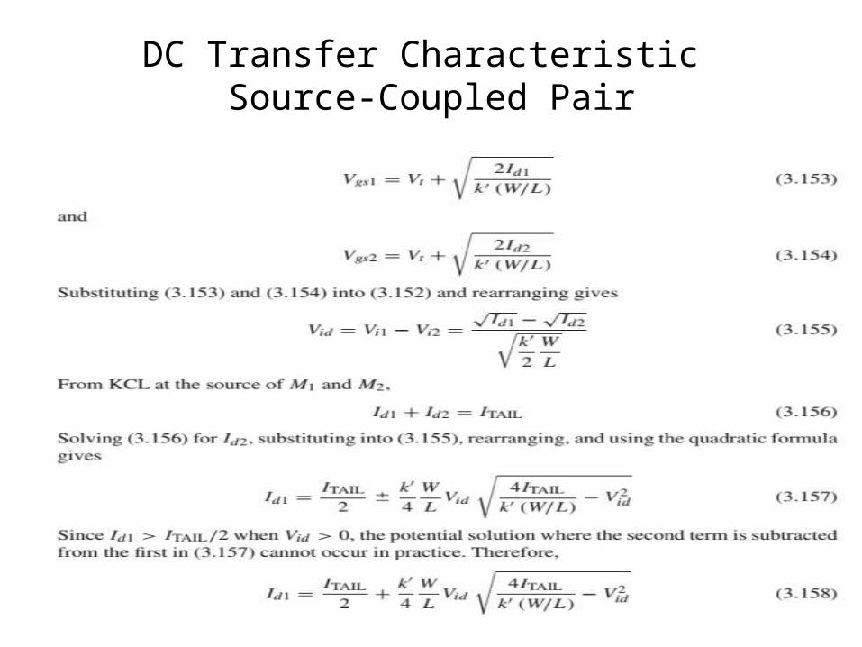
• From KVL around the input loop,Vi1−Vgs1+Vgs2−Vi2=0
• We assume that the drain resistors are small enough that neither transistor operates in the triode region ifVi1≤VDDandVi2≤VDD.
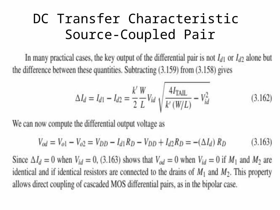
• Furthermore, we assume that the drain current of each transistor is related to its gate-source voltage by the approximate square-law relationship given in (1.157). If the transistors are identical, applying (1.157) to each transistor and rearranging gives
DC Transfer Characteristic Source-Coupled Pair

DC Transfer Characteristic Source-Coupled Pair
DC Transfer Characteristic Source-Coupled Pair

DC Transfer Characteristic Source-Coupled Pair

• Equation 3.161 shows that the range of Vid for which both transistors operate in the active region is proportional to the overdrive calculated when Vid =0. This result is illustrated in Fig. 3.51.
• The overdrive is an important quantity in MOS circuit design, affecting not only the input range of differential pairs, but also other characteristics including the speed, offset, and output swing of MOS amplifiers.
• Since the overdrive of an MOS transistor depends on its current and W/L ratio, the range of a source-coupled pair can be adjusted to suit a given application by adjusting the value of the tail current and/or the aspect ratio of the input devices.
DC Transfer Characteristic Source-Coupled Pair
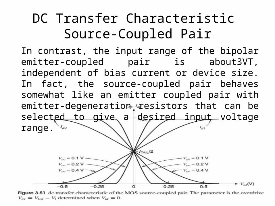
In contrast, the input range of the bipolar emitter-coupled pair is about3VT, independent of bias current or device size. In fact, the source-coupled pair behaves somewhat like an emitter coupled pair with emitter-degeneration resistors that can be selected to give a desired input voltage range.
DC Transfer Characteristic Source-Coupled Pair
DC Transfer Characteristic Source-Coupled Pair

Small-Signal Characteristics of Balanced Differential Amplifiers
• In this section, we will study perfectly balanced differential amplifiers. Therefore, Acm−dm=0 and Adm−cm=0 here, and our goal is to calculate Adm and Acm. Although calculating Adm and Acm from the entire small-signal equivalent circuit of a differential amplifier is possible, these calculations are greatly simplified by taking advantage of the symmetry that exists in perfectly balanced amplifiers. In general, we first find the response of a given circuit to pure differential and pure common-mode inputs separately. Then the results can be superposed to find the total solution.
• Since superposition is valid only for linear circuits, the following analysis is strictly valid only from a small-signal standpoint and approximately valid only for signals that cause negligible nonlinearity.
• In previous sections, we carried out large-signal analyses of differential pairs and assumed that the Norton-equivalent resistance of the tail current source was infinite.

• Since this resistance has a considerable effect on the small-signal behavior of differential pairs, however, we now assume that this resistance is finite. Because the analysis here is virtually the same for both bipolar and MOS differential pairs, the two cases will be considered together.
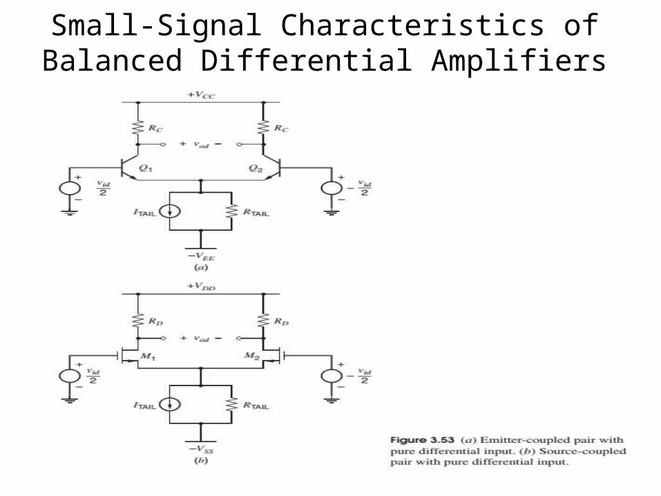
• Consider the bipolar emitter-coupled pair of Fig. 3.45 and the MOS source-coupled pair of Fig. 3.50 from a small-signal standpoint. ThenVi1=vi1andVi2=vi2. These circuits are redrawn in Fig. 3.53aand Fig. 3.53bwith the common-mode input voltages set to zero so we can consider the effect of the differential-mode input by itself.
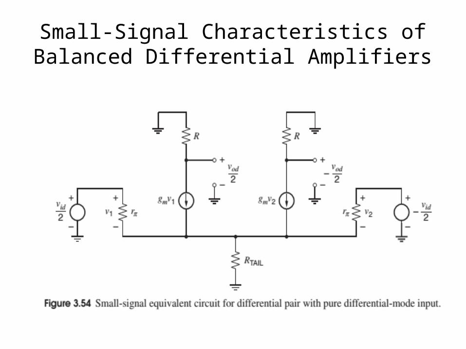
• The small-signal equivalent circuit for both cases is shown in Fig. 3.54 with R used to replace RC in Fig. 3.53aandRDin 3.53b. Note that the small-signal equivalent circuit neglects finite ro in both cases. Also, in the MOS case, non zero gmb is ignored and rπ→∞ becauseβ0→∞.
Small-Signal Characteristics of Balanced Differential Amplifiers

• Because the circuit in Fig. 3.54 is perfectly balanced, and because the inputs are driven by equal and opposite voltages, the voltage across RTAIL does not vary at all. Another way to see this result is to view the two lower parts of the circuit as voltage followers.
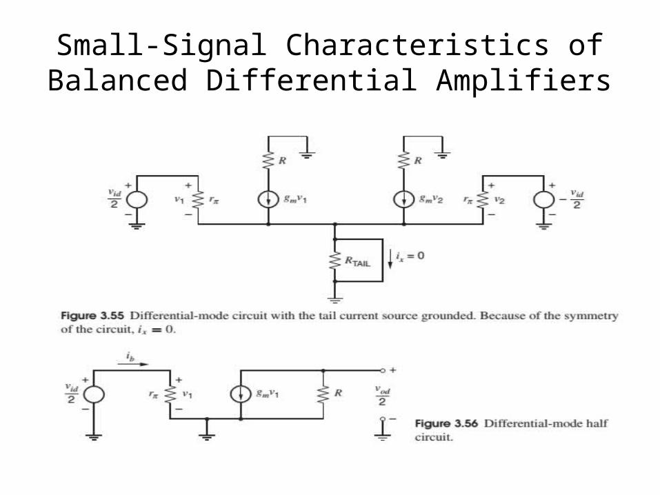
• When one side pulls up, the other side pulls down, resulting in a constant voltage across the tail current source by superposition. Since the voltage across RTAIL experiences no variation, the behavior of the small-signal circuit is unaffected by the placement of a short circuit across RTAIL, as shown in Fig. 3.55.
• After placing this short circuit, we see that the two sides of the circuit are not only identical, but also independent because they are joined at a node that operates as a small-signal ground.
• Therefore, the response to small-signal differential inputs can be determined by analyzing one side of the original circuit with RTAIL replaced by a short circuit.
Small-Signal Characteristics of Balanced Differential Amplifiers
Small-Signal Characteristics of Balanced Differential Amplifiers
Small-Signal Characteristics of Balanced Differential Amplifiers
Small-Signal Characteristics of Balanced Differential Amplifiers
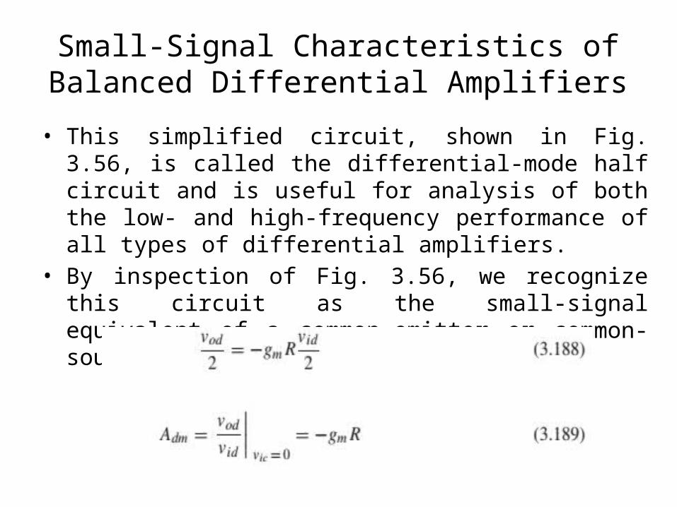
• This simplified circuit, shown in Fig. 3.56, is called the differential-mode half circuit and is useful for analysis of both the low- and high-frequency performance of all types of differential amplifiers.
• By inspection of Fig. 3.56, we recognize this circuit as the small-signal equivalent of a common-emitter or common-source amplifier.
Small-Signal Characteristics of Balanced Differential Amplifiers
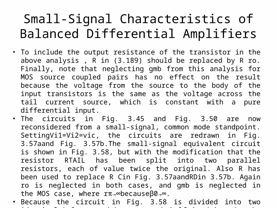
• To include the output resistance of the transistor in the above analysis , R in (3.189) should be replaced by R ro. Finally, note that neglecting gmb from this analysis for MOS source coupled pairs has no effect on the result because the voltage from the source to the body of the input transistors is the same as the voltage across the tail current source, which is constant with a pure differential input.
• The circuits in Fig. 3.45 and Fig. 3.50 are now reconsidered from a small-signal, common mode standpoint. SettingVi1=Vi2=vic, the circuits are redrawn in Fig. 3.57aand Fig. 3.57b.The small-signal equivalent circuit is shown in Fig. 3.58, but with the modification that the resistor RTAIL has been split into two parallel resistors, each of value twice the original. Also R has been used to replace R Cin Fig. 3.57aandRDin 3.57b. Again ro is neglected in both cases, and gmb is neglected in the MOS case, where rπ→∞becauseβ0→∞.
• Because the circuit in Fig. 3.58 is divided into two identical halves, and because each half is driven by the same voltage vic , no current ix flows in the lead connecting the half circuits. The circuit behavior is thus unchanged when this lead is removed as shown in Fig. 3.59. As a result, we see that the two halves of the circuit in Fig. 3.58 are not only identical, but also independent because they are joined by a branch that conducts no small-signal current.
Small-Signal Characteristics of Balanced Differential Amplifiers

• Therefore, the response to small-signal, common-mode inputs can be determined by analyzing one half of the original circuit with an open circuit replacing the branch that joins the two halves of the original circuit.
• This simplified circuit, shown in Fig. 3.60, is called the common mode half circuit. By inspection of Fig. 3.60, we recognize this circuit as a common-emitter or common-source amplifier with degeneration. Then voc=−GmRvic (3.190)
Small-Signal Characteristics of Balanced Differential Amplifiers

Small-Signal Characteristics of Balanced Differential Amplifiers

Small-Signal Characteristics of Balanced Differential Amplifiers

Where Gm is the transconductance of a common-emitter or common-source amplifier with degeneration and will be considered quantitatively below. Since degeneration reduces the transconductance, and since degeneration occurs only in the common-mode case, (3.189) and (3.191) show that |Adm|>|Acm|; therefore, the differential pair is more sensitive to differential inputs than to common-mode inputs. In other words, the tail current source provides local negative feedback to common-mode inputs (or local common-mode feedback).
Small-Signal Characteristics of Balanced Differential Amplifiers

Bipolar Emitter-Coupled Pair.
• For the bipolar case, substituting (3.93) for Gm with RE=2RTAIL into (3.191) and rearranging give
• To include the effect of finite ro in the above analysis, R in (3.192) should be replaced by RRo, Where Ro is the output resistance of a common-emitter amplifier with emitter degeneration of RE=2RTAIL, given in (3.97) or (3.98). This substitution ignores the effect of finite ro on Gm, which is shown in (3.92) and is usually negligible.
• The CMRR is found by substituting (3.189) and (3.192) into (3.187), which gives CMRR=1+2gmRTAIL (3.193)This expression applies to the particular case of a single-stage, emitter-coupled pair. It shows that increasing the output resistance of the tail current source RTAIL improves the common mode-rejection ratio.

• Since bipolar transistors have finite β0, and since differential amplifiers are often used as the input stage of instrumentation circuits, the input resistance of emitter-coupled pairs is also an important design consideration. The differential input resistance Rid is defined as the ratio of the small-signal differential input voltage vid to the small-signal input current ib when a pure differential input voltage is applied. By inspecting Fig. 3.56, we find that
Bipolar Emitter-Coupled Pair.

• Thus the differential input resistance depends on the rπof the transistor, which increases withincreasing β0 and decreasing collector current. High input resistance is therefore obtained when an emitter-coupled pair is operated at low bias current levels. The common-mode input resistance Ric is defined as the ratio of the small-signal, common mode input voltage vic to the small-signal input current ib in one terminal when a pure common mode input is applied. Since the common-mode half circuit in Fig. 3.60 is the same as that for a common-emitter amplifier with emitter degeneration, substituting RE=2RTAILinto (3.90) gives Ric as
Bipolar Emitter-Coupled Pair.

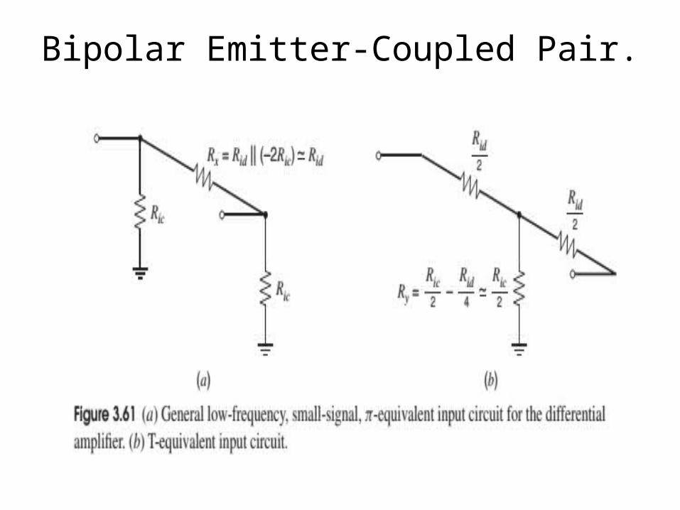
• The input resistance can be represented by theπequivalent circuit of Fig. 3.61a or by the T-equivalent circuit of Fig. 3.61b.
• For the πmodel, the common-mode input resistance is exactly Ric independent of Rx. To make the differential-mode input resistance exactly Rid, the value of Rx should be more than Rid to account for nonzero current in Ric .
• On the other hand, for the T model, the differential-mode input resistance is exactly Rid independent of Ry, and the common-mode input resistance is Ric if Ry is chosen to be less than Ric/2 as shown.
• The approximations in Fig. 3.61 are valid if Ric is much larger than Rid
Bipolar Emitter-Coupled Pair.
Bipolar Emitter-Coupled Pair.
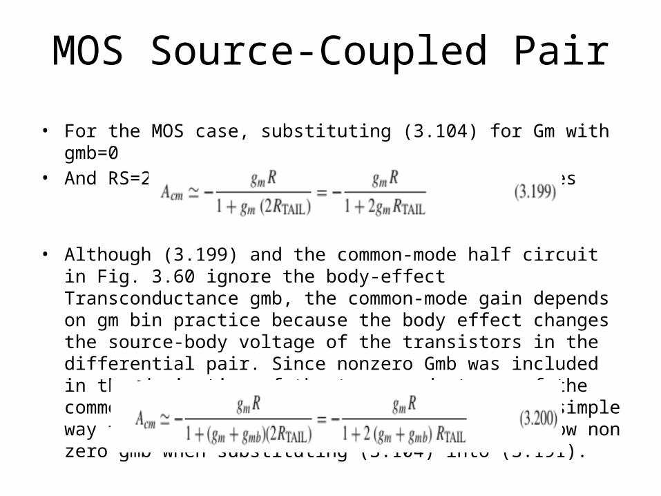
MOS Source-Coupled Pair
• For the MOS case, substituting (3.104) for Gm with gmb=0• And RS=2RTAILinto (3.191) and rearranging gives
• Although (3.199) and the common-mode half circuit in Fig. 3.60 ignore the body-effect Transconductance gmb, the common-mode gain depends on gm bin practice because the body effect changes the source-body voltage of the transistors in the differential pair. Since nonzero Gmb was included in the derivation of the transconductance of the common-source amplifier with degeneration, a simple way to include the body effect here is to allow non zero gmb when substituting (3.104) into (3.191).

• To include the effect of finite ro in the above analysis, Rin (3.199) and (3.200) should be replaced by RRo, where Ro is the output resistance of a common-source amplifier with source degeneration of RS=2RTAIL, given in (3.107). This substitution ignores the effect of finite ro on Gm, which is shown in (3.103) and is usually negligible. The CMRR is found by substituting (3.189) and (3.200) into (3.187), which gives
• CMRR1+2(gm+gmb) RTAIL (3.201)• Equation 3.201 is valid for a single-stage, source-coupled pair
and shows that increasing RTAIL increases the CMRR.
MOS Source-Coupled Pair


![Unit 1 Unit 2 Unit 3 Unit 4 Unit 5 Unit 6 Unit 7 Unit 8 ... 5 - Formatted.pdf · Unit 1 Unit 2 Unit 3 Unit 4 Unit 5 Unit 6 ... and Scatterplots] Unit 5 – Inequalities and Scatterplots](https://img.pdfslide.net/doc/110x75/5b76ea0a7f8b9a4c438c05a9/unit-1-unit-2-unit-3-unit-4-unit-5-unit-6-unit-7-unit-8-5-formattedpdf.jpg)