Embed Size (px)
Citation preview
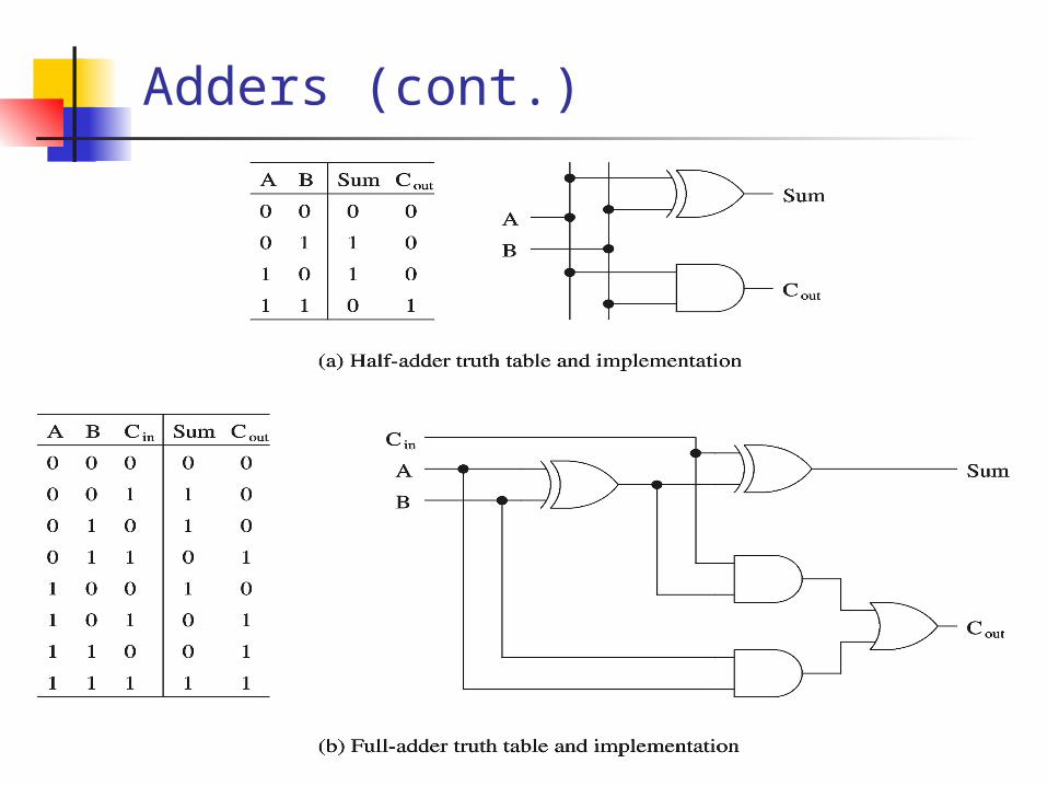
Adders
Half-adder Adds two bits
Produces a sum and carry Problem: Cannot use it to build larger inputs
Full-adder Adds three 1-bit values
Like half-adder, produces a sum and carry Allows building N-bit adders
Simple technique Connect Cout of one adder to Cin of the next
These are called ripple-carry adders
Adders (cont.)
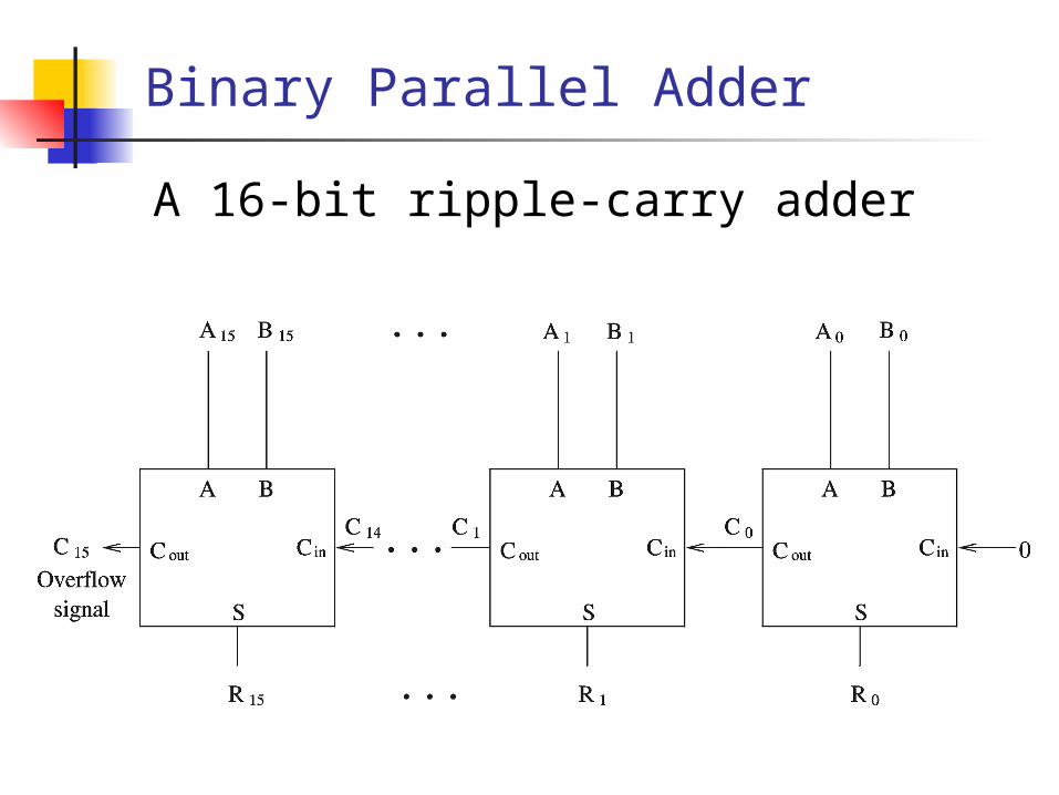
Binary Parallel Adder
A 16-bit ripple-carry adder

BCD Adder
In BCD, we have only ten combinations from 0000 to
1001. These combinations represent 0 to 9 in binary
using 8421 code.
When the sum of two digits is less than or equal to 9
then the ordinary 4-bit adder can be used
But if the sum of two digits is greater than 9 then a
correction factor must be added “ie 6,(0110) to the
result.”
We need to design a circuit that is capable of doing the
correct addition

BCD Adder
The cases where the sum of two 4-bit numbers is greater than 9 are in the following table:
S4 S3 S2 S1 S0
0 1 0 1 0 10
0 1 0 1 1 11
0 1 1 0 0 12
0 1 1 0 1 13
0 1 1 1 0 14
0 1 1 1 1 15
1 0 0 0 0 16
1 0 0 0 1 17
1 0 0 1 0 18

BCD Adder
Whenever S4=1 (sums greater than 15)
Whenever S3=1 and either S2 or S1 or both
are 1 (sums 10 to 15)
The previous table can be expressed as:
X = S4 + S3 ( S2 + S1)
So, whenever X = 1 we should add a
correction of 0110 to the sum.

0011
0101
0 1 0 0 0
0
00
1000
0000
Inputs:[A]=0101, [B]= 0011, Co=0
1 0 0 0
1

0110
0111
0 1 1 0 1
1
11
1101
0110
Inputs:[A]=0111, [B]= 0110, Co=0
0 0 1 1
1

Half Subtractor
It is logic circuit that subtracts one bit from another bit and produces two outputs as Difference (Diff) and Borrow (Br).
With A and B as inputs, and Diff and Br as the two outputs.
A Diff
B Br
H/S

Half Subtractor
Br A B D 0 0 iff
0 0 0 00 1 1 11 0 1 01 1 0 0
A 0 B 0
D iff
Br
0-1 1
21

Full Subtractors
It is a combinational circuit that performs the arithmetic subtraction of three input bits.
It consists of three inputs and two outputs. Two of the input variables denoted by A and B
represents the two significant bits to be subtracted.
The third input C represents the borrow taken from the next higher significant position.
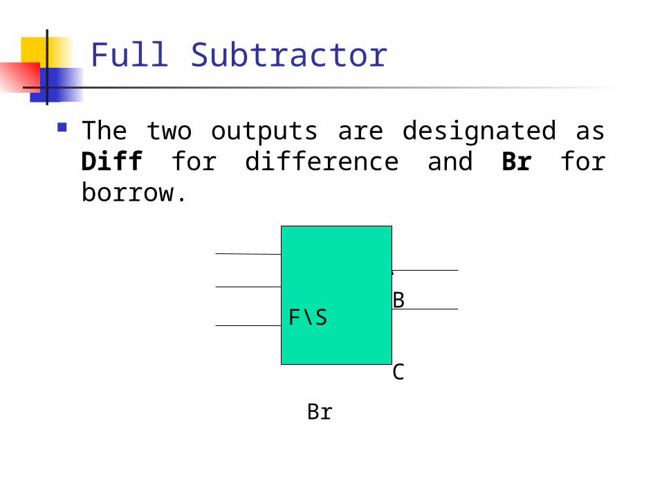
Full Subtractor
The two outputs are designated as Diff for difference and Br for borrow.
A B Diff
C Br F\S
Full Subtractor
The 1’s and 0’s for the output variables are determined
from the subtraction of A-B-C.
For A=0, B=0, and C=1, we have to borrow a 1 from the
next stage, which makes Br=1 and adds 2 to A. Since 2-
0-1=1, Diff = 1.
For A=0 and BC=11, we need to borrow again, making
Br=1 and A=2. Since 2-1-1=0, Diff = 0.
For A=1,B=1 and C=1, we have to borrow 1, making
Br=1 and A=3. Since 3-1-1=1 making Diff = 1.

Full Subtractor
0 0 0 0 00 0 1 1 10 1 0 1 10 1 1 1 01 0 0 0 11 0 1 0 01 1 0 0 01 1 1 1 1
A B C Br Diff
1 1
1 1
Ci
AiBi
00 01 11 10
0
1
Diff
Same as Si in full adder

Full Subtractor
0 0 0 0 00 0 1 1 10 1 0 1 10 1 1 1 01 0 0 0 11 0 1 0 01 1 0 0 01 1 1 1 1
A B C Br Diff Ci
AiBi
00 01 11 10
0
1
Br
1 1 1
1
1 11
1
1 1

Adders (cont.)
Ripple-carry adders can be slow Delay proportional to number of bits
Carry lookahead adders Eliminate the delay of ripple-carry adders Carry-ins are generated independently
C0 = A0 B0
C1 = A0 B0 A1 + A0 B0 B1 + A1 B1
. . . Requires complex circuits Usually, a combination carry lookahead and
ripple-carry techniques are used

Introduction to Combinational Circuits
Combinational circuits Output depends only on the current inputs
Combinational circuits provide a higher level of abstraction Help in reducing design complexity Reduce chip count
We look at some useful combinational circuits

Examples of Combinational Circuits
a) Decoders b) Encoders c) Multiplexers d) Demultiplexers

Integrated Circuits
An integrated circuit is a piece (also called a chip)
of silicon on which multiple gates or transistors
have been embedded
These silicon pieces are mounted on a plastic or
ceramic package with pins along the edges that can
be soldered onto circuit boards or inserted into
appropriate sockets

Integrated Circuits
SSI, MSI, LSI: They perform small tasks such as addition of few
bits. small memories, small processors
VLSI Tasks: - Large memory - Complex microprocessors, CPUs

Multiplexers – (Many to One)
Multiplexing means transmitting a large number of
information units over a smaller number of channels or lines.
A Digital Multiplexer is a combinational circuit that selects
binary information from one of many input lines and directs it
to a single output line.
The selection of a particular input line is controlled by a set of
selection lines.
Normally, 2^n input lines and n selection lines whose bit
combinations determine which input is selected.

Multiplexer (MUX):
A MUX is a digital switch that
has multiple inputs (sources)
and a single output
(destination).
The select lines determine which
input is connected to the output.
MUX Types 2-to-1 (1 select line) 4-to-1 (2 select lines) 8-to-1 (3 select lines) 16-to-1 (4 select lines)
22
Multiplexer Block Diagram
SelectLines
Inputs(sources)
Output(destination)
12N
N
MU
X

Typical Application of a MUX
23
MP3 PlayerDocking Station
Laptop Sound Card
DigitalSatellite
DigitalCable TV
Surround Sound System
MU
X
D0
D1
D2
D3
Y
B ASelected Source
0 0 MP3
0 1 Laptop
1 0 Satellite
1 1 Cable TV
Multiple Sources Single DestinationSelector

Medium Scale Integration MUX
4-to-1 MUX 8-to-1 MUX 16-to-1 MUX
24
Inputs
Select
Enable
Output (Y)(and inverted output)

Multiplexers
Multiplexer 2n data inputs n selection inputs a single output
Selection input
determines the input
that should be
connected to the
output
4-data input MUX

Multiplexers - Strobe/Enable Input
When we may have to combine a no. of multiplexers and
enable only one of the multiplexer.
So, Strobe/Enable input is included in multiplexer chips(ICs).
It can be “active high” or “active low”.
Multiplexer is Enabled when strobe is high and Disabled when
strobe is low.
When the strobe/enable terminal is in “0” state, the output of
all the AND gates become “0” and the final output is also “0”.
Under this condition, the multiplexer is said to be disabled.
When the strobe input is in “1” state, all the four AND gates are
enabled and the circuit functions normally as a multiplexer.

Multiplexers (cont.)
4-data input MUX implementation

Demultiplexer (DEMUX):(One to Many)
It is the reverse of multiplexer.
A DEMUX is a digital switch with a single input (source) and a multiple outputs (destinations).
The select lines determine which output the input is connected to.
DEMUX Types 1-to-2 (1 select line) 1-to-4 (2 select lines) 1-to-8 (3 select lines) 1-to-16 (4 select lines)
28
Demultiplexer Block Diagram
SelectLines
Input(source)
Outputs(destinations)
2N1
N
DE
MU
X

Typical Application of a DEMUX
29
Single Source Multiple DestinationsSelector
D0
D1
D2
D3
X
DE
MU
X
B ASelected
Destination
0 0 B/W Laser Printer
0 1 Fax Machine
1 0 Color Inkjet Printer
1 1 Pen Plotter
B/W LaserPrinter
Color InkjetPrinter
PenPlotter
FaxMachine
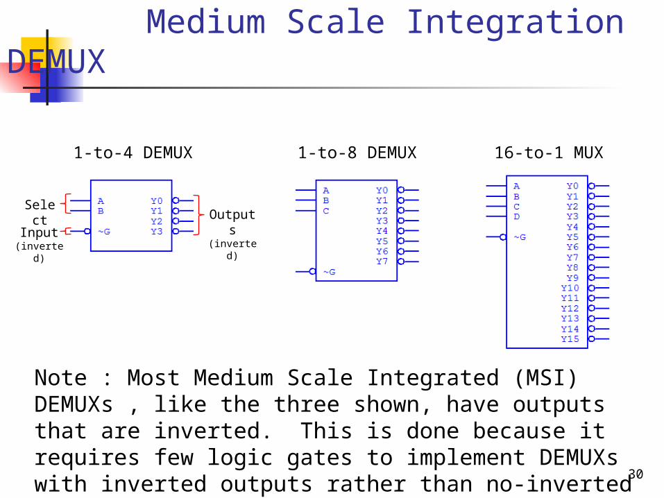
Medium Scale Integration DEMUX
1-to-4 DEMUX 1-to-8 DEMUX 16-to-1 MUX
30
Select
Input(inverted)
Outputs(inverted)
Note : Most Medium Scale Integrated (MSI) DEMUXs , like the three shown, have outputs that are inverted. This is done because it requires few logic gates to implement DEMUXs with inverted outputs rather than no-inverted outputs.

Demultiplexers
S1 S0 O0 O1 O2 O3
0 0 I 0 0 0
0 1 0 I 0 0
1 0 0 0 I 0
1 1 0 0 0 I
Function Table

Encoder/Decoder VocabularyEncoder/Decoder Vocabulary
ENCODER- a digital circuit that produces a
binary output code depending on which of its
inputs are activated.
DECODER- a digital circuit that converts an
input binary code into a single numeric output.
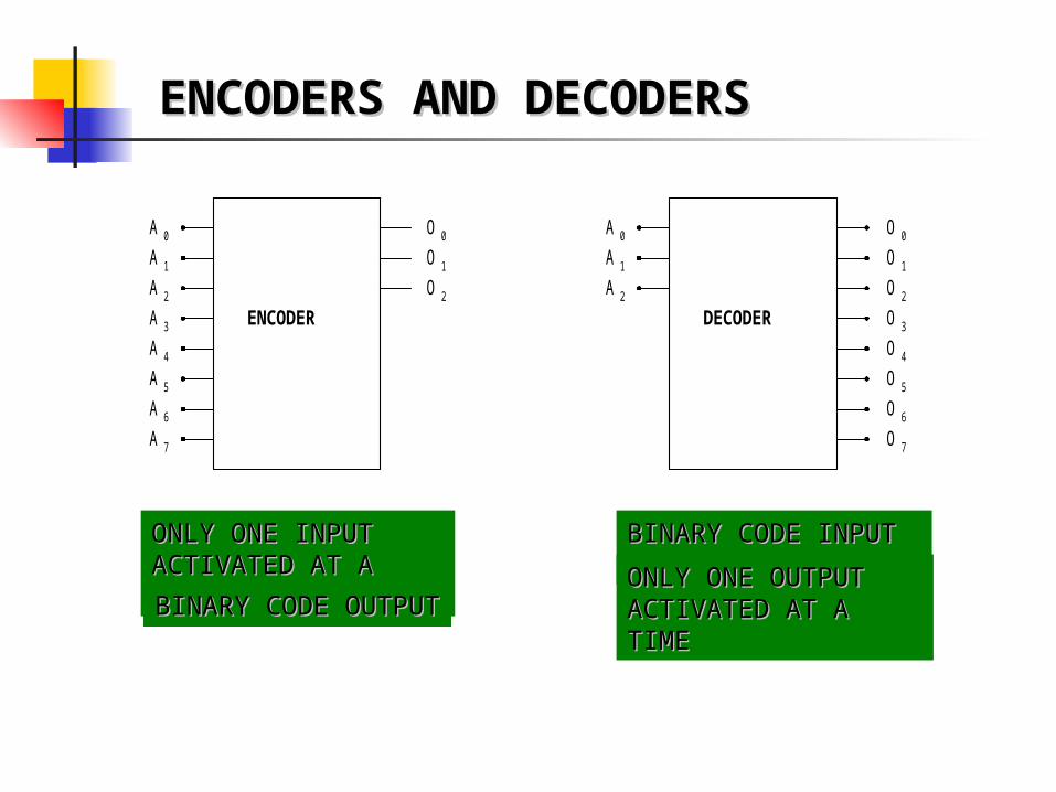
ENCODERS AND DECODERSENCODERS AND DECODERS
A 0
A 1
A 2
A 3
A 4
A 5
A 6
A 7
ENCODER
O 0
O 1
O 2
A 0
A 1
A 2
O 0
O 1
O 2
O 3
O 4
O 5
O 6
O 7
DECODER
ONLY ONE INPUT ONLY ONE INPUT ACTIVATED AT A TIMEACTIVATED AT A TIME
BINARY CODE OUTPUTBINARY CODE OUTPUT
BINARY CODE INPUTBINARY CODE INPUT
ONLY ONE OUTPUT ONLY ONE OUTPUT ACTIVATED AT A TIMEACTIVATED AT A TIME

Decoder
• A decoder is a logic circuit that accepts a set of inputs
that represents a binary number and activates only
the output that corresponds to the input number. It has n address lines and 2^n outputs.
For a given address, only one of the outputs goes
high and remaining outputs remain in low state. It is
said to have “active high outputs”.
For a given address, only one of the outputs goes low
while the remaining outputs remain in high state. It
is said to have “active low outputs”.

2 to 4 Decoder
Function Table:

3 to 8 Decoder
Logic function implementation
(Full Adder)
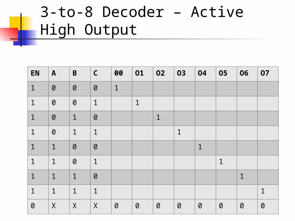
3-to-8 Decoder – Active High Output
EN A B C 00 O1 O2 O3 O4 O5 O6 O7
1 0 0 0 1
1 0 0 1 1
1 0 1 0 1
1 0 1 1 1
1 1 0 0 1
1 1 0 1 1
1 1 1 0 1
1 1 1 1 1
0 X X X 0 0 0 0 0 0 0 0
3-8 Line Decoder (Active-HIGH)

BCD -to- Decimal Decoders
•The BCD- to-decimal decoder converts each BCD code into one of Ten Positionable decimal digit indications. It is frequently referred as a 4-line -to- 10 line decoder
•The method of implementation is that only ten decoding gates are required because the BCD code represents only the ten decimal digits 0 through 9.
•It has four inputs and 10 outputs. Depending on the BCD input, one of the outputs goes to ‘0’ state while the remaining nine outputs go to ‘1’ state.

40
Logic diagram of BCD - decimal decoder(Active LOW output)
Encoder
•An encoder is a combinational logic circuit that essentially performs a “reverse” of decoder functions.
•An encoder accepts an active level on one of its inputs, representing digit, such as a decimal or octal digits, and converts it to a coded output such as BCD or binary.
•Encoders can also be devised to encode various symbols and alphabetic characters.
•The process of converting from familiar symbols or numbers to a coded format is called encoding.

42
Most decoders accept an input code and produce a HIGH
( or a LOW) at one and only one output line.
In otherwords, a decoder identifies, recognizes, or detects a
particular code. The opposite of this decoding process is called
Encoding and is performed by a logic circuit called an
Encoder.
An encoder has a number of input lines, only one of which
input is activated at a given time and produces an N-bit output
code, depending on which input is activated.
Encoder

General Encoder Diagram
44
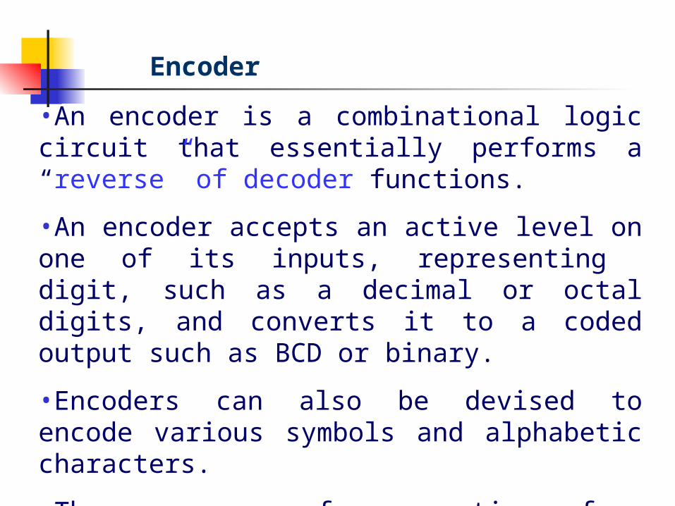
Logic circuit for Octal-to Binary Encoder [8-line- 3-line ]

45
A low at any single input will produce the output binary code corresponding to that input. For instance , a low at A3’ will produce O2 =0, O1=1 and O0 =1, which is binary code for 3. Ao’ is not connected to the logic gates because the encoder outputs always be normally at 0000 when none of the inputs is LOW
Truth table for Octal-to Binary Encoder [8-line- 3-line ]

1-bit Arithmetic and Logic Unit
Preliminary ALU design
2’s complementRequired 1 is added via Cin

1-bit Arithmetic and Logic Unit (cont.)
Final design
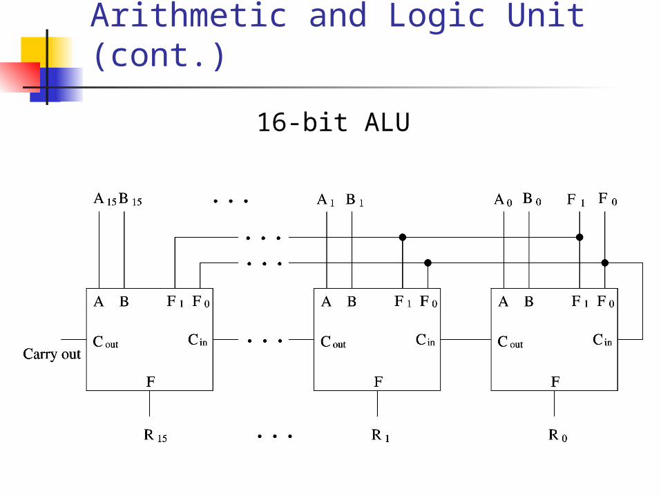
Arithmetic and Logic Unit (cont.)
16-bit ALU

Arithmetic and Logic Unit (cont’d)
4-bit ALU

Introduction to Sequential Circuits
Output depends on current as well as past inputs Depends on the history Have “memory” property
Sequential circuit consists of Combinational circuit Feedback circuit
Past input is encoded into a set of state variables Uses feedback (to feed the state variables)
Simple feedback Uses flip flops
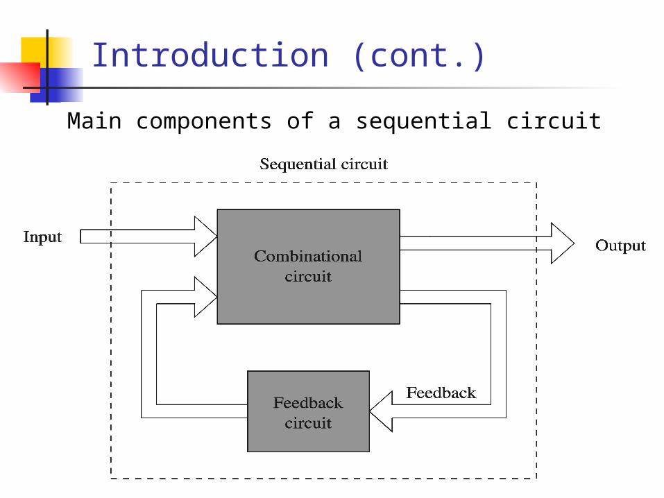
Introduction (cont.)
Main components of a sequential circuit

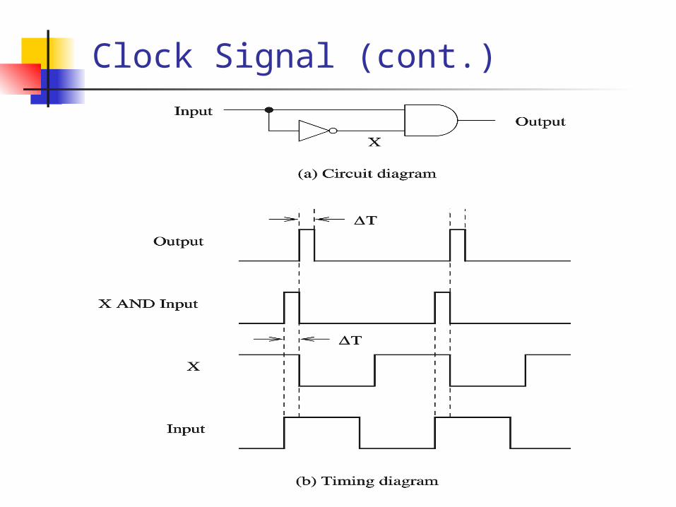
Clock Signal

Clock Signal (cont.)
Clock serves two distinct purposes Synchronization point
Start of a cycle End of a cycle Intermediate point at which the clock signal
changes levels Timing information
Clock period, ON, and OFF periods Propagation delay
Time required for the output to react to changes in the inputs
Clock Signal (cont.)

Latches
Can remember a bit Level-sensitive (not edge-sensitive)
A NOR gate implementation of SR latch

Latches (cont.)
SR latch outputs follow inputs In clocked SR latch, outputs respond at specific
instances Uses a clock signal
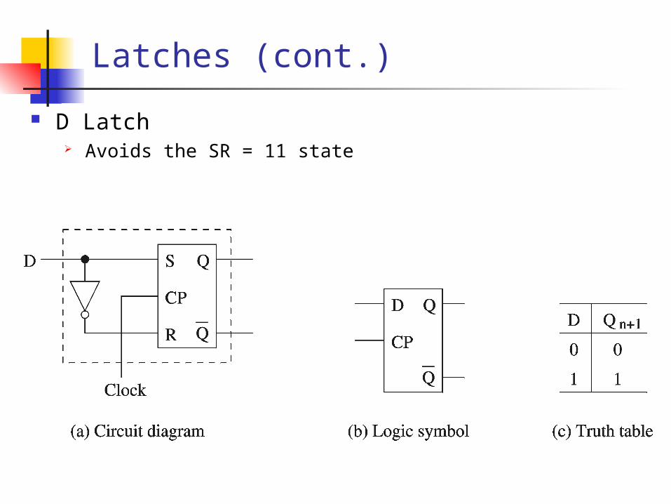
Latches (cont.)
D Latch Avoids the SR = 11 state

Flip-Flops
Edge-sensitive devices Changes occur either at positive or negative edges
Positive edge-triggered D flip-flop

Flip-Flops (cont.)
Notation Not strictly followed in the literature
We follow the following notation for latches and flip-flops
Low level High level Positive edge Negative edge
Latches Flip-flops

Flip-Flops (cont.)

Example Sequential Circuits (cont.)
74164 shift
Register chip

Memory Design with D Flip FlopsRequire separate data in and out lines