Embed Size (px)
Citation preview
This is information on a product in full production.
November 2013 DocID2572 Rev 33 1/44
44
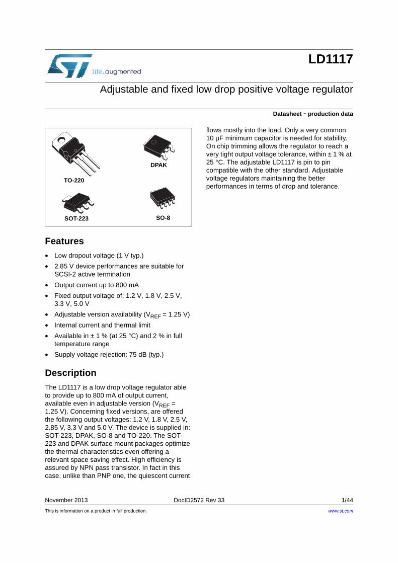
LD1117
Adjustable and fixed low drop positive voltage regulator
Datasheet - production data
Features• Low dropout voltage (1 V typ.)
• 2.85 V device performances are suitable for SCSI-2 active termination
• Output current up to 800 mA
• Fixed output voltage of: 1.2 V, 1.8 V, 2.5 V, 3.3 V, 5.0 V
• Adjustable version availability (VREF = 1.25 V)
• Internal current and thermal limit
• Available in ± 1 % (at 25 °C) and 2 % in full temperature range
• Supply voltage rejection: 75 dB (typ.)
DescriptionThe LD1117 is a low drop voltage regulator able to provide up to 800 mA of output current, available even in adjustable version (VREF = 1.25 V). Concerning fixed versions, are offered the following output voltages: 1.2 V, 1.8 V, 2.5 V, 2.85 V, 3.3 V and 5.0 V. The device is supplied in: SOT-223, DPAK, SO-8 and TO-220. The SOT-223 and DPAK surface mount packages optimize the thermal characteristics even offering a relevant space saving effect. High efficiency is assured by NPN pass transistor. In fact in this case, unlike than PNP one, the quiescent current
flows mostly into the load. Only a very common 10 µF minimum capacitor is needed for stability. On chip trimming allows the regulator to reach a very tight output voltage tolerance, within ± 1 % at 25 °C. The adjustable LD1117 is pin to pin compatible with the other standard. Adjustable voltage regulators maintaining the better performances in terms of drop and tolerance.
TO-220
DPAK
SOT-223 SO-8
www.st.com
Contents LD1117
2/44 DocID2572 Rev 33
Contents
1 Diagram . . . . . . . . . . . . . . . . . . . . . . . . . . . . . . . . . . . . . . . . . . . . . . . . . . . 5
2 Pin configuration . . . . . . . . . . . . . . . . . . . . . . . . . . . . . . . . . . . . . . . . . . . 6
3 Maximum ratings . . . . . . . . . . . . . . . . . . . . . . . . . . . . . . . . . . . . . . . . . . . . 7
4 Schematic application . . . . . . . . . . . . . . . . . . . . . . . . . . . . . . . . . . . . . . . 8
5 Electrical characteristics . . . . . . . . . . . . . . . . . . . . . . . . . . . . . . . . . . . . . 9
6 Typical application . . . . . . . . . . . . . . . . . . . . . . . . . . . . . . . . . . . . . . . . . 21
7 LD1117 adjustable: application note . . . . . . . . . . . . . . . . . . . . . . . . . . . 24
8 Package mechanical data . . . . . . . . . . . . . . . . . . . . . . . . . . . . . . . . . . . . 25
9 Packing mechanical data . . . . . . . . . . . . . . . . . . . . . . . . . . . . . . . . . . . . 36
10 Order codes . . . . . . . . . . . . . . . . . . . . . . . . . . . . . . . . . . . . . . . . . . . . . . . 42
11 Revision history . . . . . . . . . . . . . . . . . . . . . . . . . . . . . . . . . . . . . . . . . . . 43
DocID2572 Rev 33 3/44
LD1117 List of tables
List of tables
Table 1. Absolute maximum ratings . . . . . . . . . . . . . . . . . . . . . . . . . . . . . . . . . . . . . . . . . . . . . . . . . . 7Table 2. Thermal data. . . . . . . . . . . . . . . . . . . . . . . . . . . . . . . . . . . . . . . . . . . . . . . . . . . . . . . . . . . . . 7Table 3. Electrical characteristics of LD1117#12 . . . . . . . . . . . . . . . . . . . . . . . . . . . . . . . . . . . . . . . . 9Table 4. Electrical characteristics of LD1117#18 . . . . . . . . . . . . . . . . . . . . . . . . . . . . . . . . . . . . . . . 10Table 5. Electrical characteristics of LD1117#25 . . . . . . . . . . . . . . . . . . . . . . . . . . . . . . . . . . . . . . . 11Table 6. Electrical characteristics of LD1117#33 . . . . . . . . . . . . . . . . . . . . . . . . . . . . . . . . . . . . . . . 12Table 7. Electrical characteristics of LD1117#50 . . . . . . . . . . . . . . . . . . . . . . . . . . . . . . . . . . . . . . . 13Table 8. Electrical characteristics of LD1117 (adjustable) . . . . . . . . . . . . . . . . . . . . . . . . . . . . . . . . 14Table 9. Electrical characteristics of LD1117#12C . . . . . . . . . . . . . . . . . . . . . . . . . . . . . . . . . . . . . . 15Table 10. Electrical characteristics of LD1117#18C . . . . . . . . . . . . . . . . . . . . . . . . . . . . . . . . . . . . . . 16Table 11. Electrical characteristics of LD1117#25C . . . . . . . . . . . . . . . . . . . . . . . . . . . . . . . . . . . . . . 17Table 12. Electrical characteristics of LD1117#33C . . . . . . . . . . . . . . . . . . . . . . . . . . . . . . . . . . . . . . 18Table 13. Electrical characteristics of LD1117#50C . . . . . . . . . . . . . . . . . . . . . . . . . . . . . . . . . . . . . . 19Table 14. Electrical characteristics of LD1117C (adjustable) . . . . . . . . . . . . . . . . . . . . . . . . . . . . . . . 20Table 15. TO-220 mechanical data (type STD-ST Dual Gauge) . . . . . . . . . . . . . . . . . . . . . . . . . . . . 25Table 16. TO-220 mechanical data (type STD-ST Single Gauge) . . . . . . . . . . . . . . . . . . . . . . . . . . . 27Table 17. SOT-223 mechanical data . . . . . . . . . . . . . . . . . . . . . . . . . . . . . . . . . . . . . . . . . . . . . . . . . 29Table 18. SO-8 mechanical data . . . . . . . . . . . . . . . . . . . . . . . . . . . . . . . . . . . . . . . . . . . . . . . . . . . . 30Table 19. DPAK mechanical data. . . . . . . . . . . . . . . . . . . . . . . . . . . . . . . . . . . . . . . . . . . . . . . . . . . . 31Table 20. Footprint data . . . . . . . . . . . . . . . . . . . . . . . . . . . . . . . . . . . . . . . . . . . . . . . . . . . . . . . . . . . 35Table 21. SOT-223 tape and reel mechanical data . . . . . . . . . . . . . . . . . . . . . . . . . . . . . . . . . . . . . . 37Table 22. SO-8 tape and reel mechanical data . . . . . . . . . . . . . . . . . . . . . . . . . . . . . . . . . . . . . . . . . 39Table 23. DPAK tape and reel mechanical data. . . . . . . . . . . . . . . . . . . . . . . . . . . . . . . . . . . . . . . . . 40Table 24. Order codes . . . . . . . . . . . . . . . . . . . . . . . . . . . . . . . . . . . . . . . . . . . . . . . . . . . . . . . . . . . . 42Table 25. Document revision history . . . . . . . . . . . . . . . . . . . . . . . . . . . . . . . . . . . . . . . . . . . . . . . . . 43
List of figures LD1117
4/44 DocID2572 Rev 33
List of figures
Figure 1. Block diagram . . . . . . . . . . . . . . . . . . . . . . . . . . . . . . . . . . . . . . . . . . . . . . . . . . . . . . . . . . . . 5Figure 2. Pin connections (top view) . . . . . . . . . . . . . . . . . . . . . . . . . . . . . . . . . . . . . . . . . . . . . . . . . . 6Figure 3. Application circuit (for 1.2 V) . . . . . . . . . . . . . . . . . . . . . . . . . . . . . . . . . . . . . . . . . . . . . . . . . 8Figure 4. Application circuit (for other fixed output voltages) . . . . . . . . . . . . . . . . . . . . . . . . . . . . . . . . 8Figure 5. Negative supply . . . . . . . . . . . . . . . . . . . . . . . . . . . . . . . . . . . . . . . . . . . . . . . . . . . . . . . . . 21Figure 6. Circuit for increasing output voltage . . . . . . . . . . . . . . . . . . . . . . . . . . . . . . . . . . . . . . . . . . 21Figure 7. Voltage regulator with reference. . . . . . . . . . . . . . . . . . . . . . . . . . . . . . . . . . . . . . . . . . . . . 21Figure 8. Battery backed-up regulated supply . . . . . . . . . . . . . . . . . . . . . . . . . . . . . . . . . . . . . . . . . . 22Figure 9. Post-regulated dual supply . . . . . . . . . . . . . . . . . . . . . . . . . . . . . . . . . . . . . . . . . . . . . . . . . 23Figure 10. Adjustable output voltage application . . . . . . . . . . . . . . . . . . . . . . . . . . . . . . . . . . . . . . . . . 24Figure 11. Adjustable output voltage application with improved ripple rejection . . . . . . . . . . . . . . . . . 24Figure 12. Drawing dimension TO-220 (type STD-ST Dual Gauge) . . . . . . . . . . . . . . . . . . . . . . . . . . 26Figure 13. Drawing dimension TO-220 (type STD-ST Single Gauge) . . . . . . . . . . . . . . . . . . . . . . . . . 28Figure 14. Drawing dimension SOT-223 . . . . . . . . . . . . . . . . . . . . . . . . . . . . . . . . . . . . . . . . . . . . . . . 29Figure 15. Drawing dimension SO-8 . . . . . . . . . . . . . . . . . . . . . . . . . . . . . . . . . . . . . . . . . . . . . . . . . . 30Figure 16. Drawing dimension DPAK (type STD-ST) . . . . . . . . . . . . . . . . . . . . . . . . . . . . . . . . . . . . . 32Figure 17. Drawing dimension DPAK (type Fujitsu-subcon.) . . . . . . . . . . . . . . . . . . . . . . . . . . . . . . . . 33Figure 18. Drawing dimension DPAK (type IDS-subcon.) . . . . . . . . . . . . . . . . . . . . . . . . . . . . . . . . . . 34Figure 19. DPAK footprint recommended data . . . . . . . . . . . . . . . . . . . . . . . . . . . . . . . . . . . . . . . . . . 35Figure 20. Drawing dimension tube for TO-220 Dual Gauge (mm.) . . . . . . . . . . . . . . . . . . . . . . . . . . 36Figure 21. Drawing dimension tube for TO-220 Single Gauge (mm.) . . . . . . . . . . . . . . . . . . . . . . . . . 36Figure 22. Tape for SOT-223 (dimensions are in mm) . . . . . . . . . . . . . . . . . . . . . . . . . . . . . . . . . . . . 37Figure 23. Reel for STO-223 (dimensions are in mm) . . . . . . . . . . . . . . . . . . . . . . . . . . . . . . . . . . . . . 38Figure 24. SO-8 tape and reel dimensions . . . . . . . . . . . . . . . . . . . . . . . . . . . . . . . . . . . . . . . . . . . . . 39Figure 25. DPAK footprint . . . . . . . . . . . . . . . . . . . . . . . . . . . . . . . . . . . . . . . . . . . . . . . . . . . . . . . . . . 40Figure 26. Tape for DPAK . . . . . . . . . . . . . . . . . . . . . . . . . . . . . . . . . . . . . . . . . . . . . . . . . . . . . . . . . . 41Figure 27. Reel for DPAK . . . . . . . . . . . . . . . . . . . . . . . . . . . . . . . . . . . . . . . . . . . . . . . . . . . . . . . . . . 41
DocID2572 Rev 33 5/44
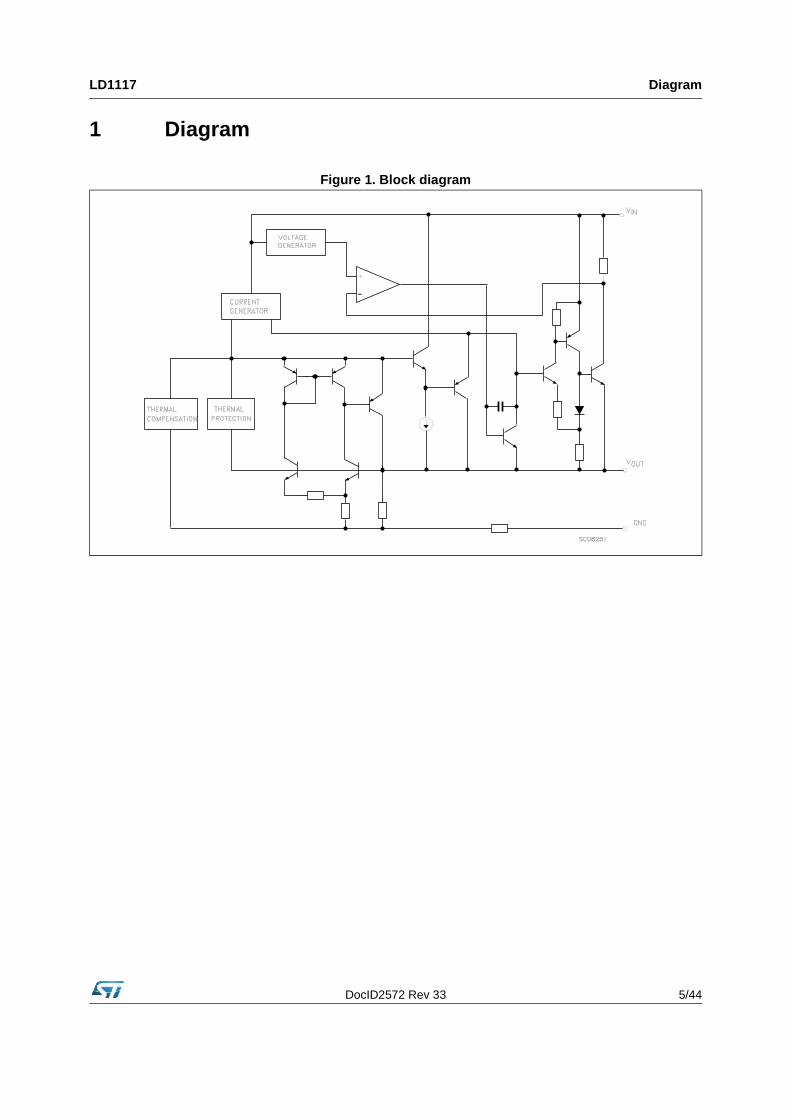
LD1117 Diagram
1 Diagram
Figure 1. Block diagram
Pin configuration LD1117
6/44 DocID2572 Rev 33
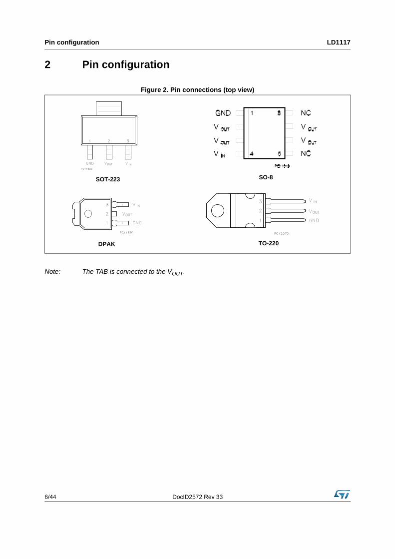
2 Pin configuration
Note: The TAB is connected to the VOUT.
Figure 2. Pin connections (top view)
SO-8
TO-220
SOT-223
DPAK
DocID2572 Rev 33 7/44
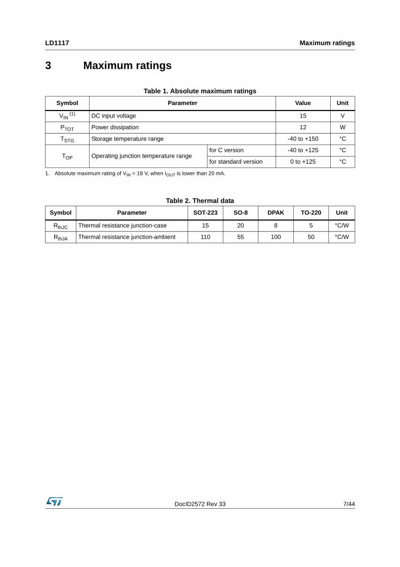
LD1117 Maximum ratings
3 Maximum ratings
Table 1. Absolute maximum ratings
Symbol Parameter Value Unit
VIN (1)
1. Absolute maximum rating of VIN = 18 V, when IOUT is lower than 20 mA.
DC input voltage 15 V
PTOT Power dissipation 12 W
TSTG Storage temperature range -40 to +150 °C
TOP Operating junction temperature rangefor C version -40 to +125 °C
for standard version 0 to +125 °C
Table 2. Thermal data
Symbol Parameter SOT-223 SO-8 DPAK TO-220 Unit
RthJC Thermal resistance junction-case 15 20 8 5 °C/W
RthJA Thermal resistance junction-ambient 110 55 100 50 °C/W
Schematic application LD1117
8/44 DocID2572 Rev 33
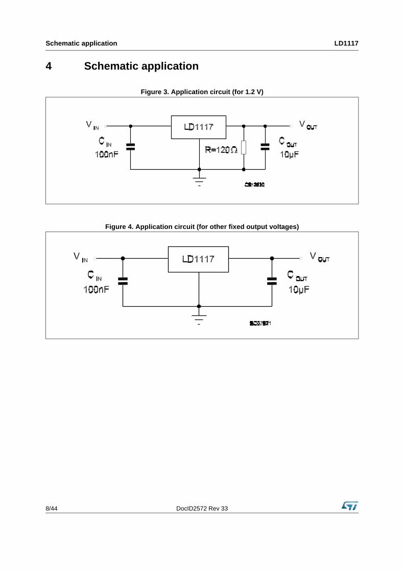
4 Schematic application
Figure 3. Application circuit (for 1.2 V)
Figure 4. Application circuit (for other fixed output voltages)
DocID2572 Rev 33 9/44
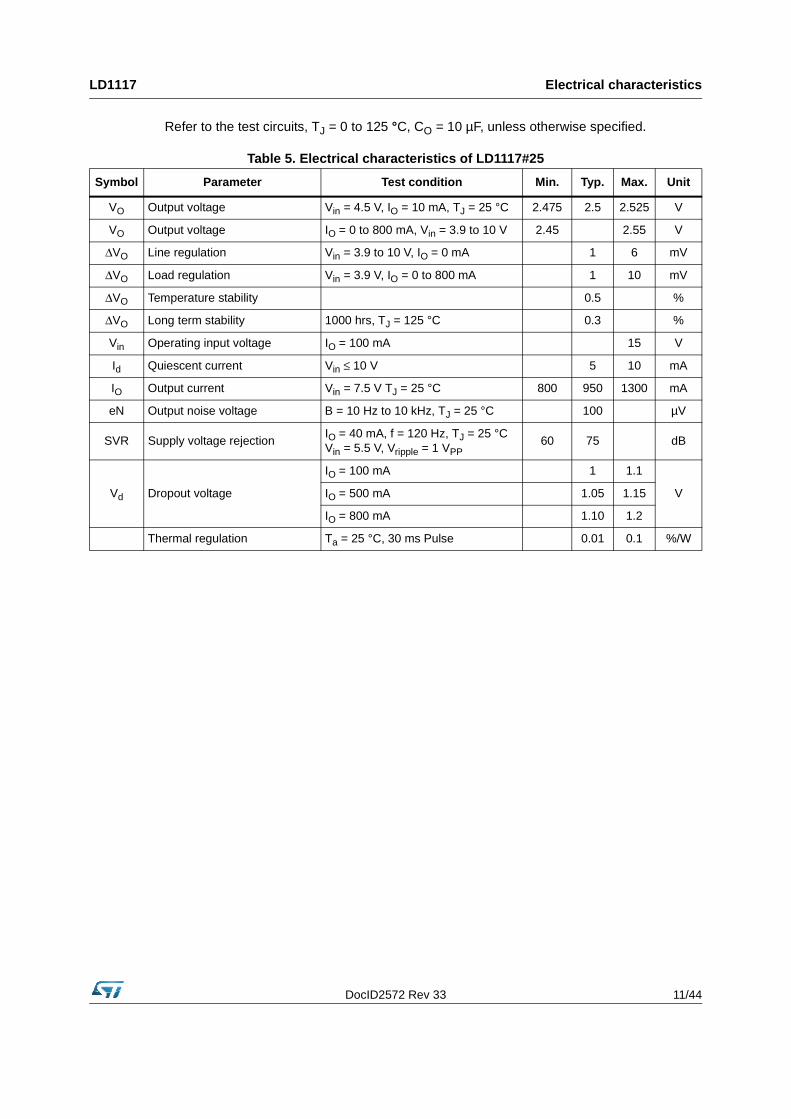
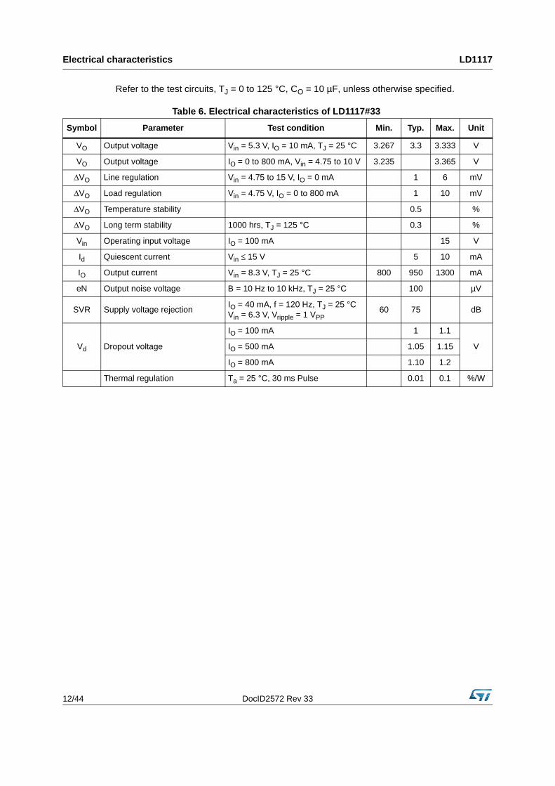
LD1117 Electrical characteristics
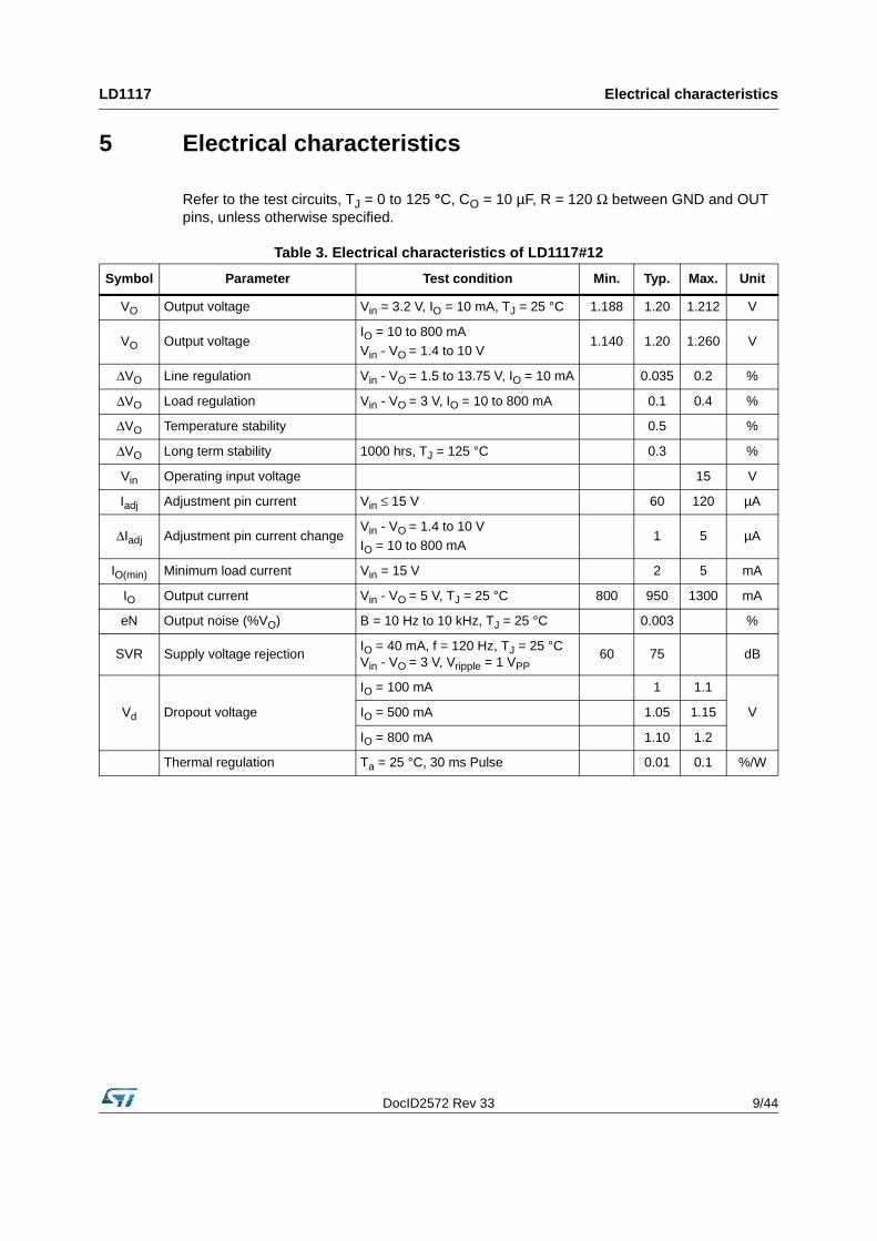
5 Electrical characteristics
Refer to the test circuits, TJ = 0 to 125 °C, CO = 10 µF, R = 120 Ω between GND and OUT pins, unless otherwise specified.
Table 3. Electrical characteristics of LD1117#12
Symbol Parameter Test condition Min. Typ. Max. Unit
VO Output voltage Vin = 3.2 V, IO = 10 mA, TJ = 25 °C 1.188 1.20 1.212 V
VO Output voltageIO = 10 to 800 mAVin - VO = 1.4 to 10 V
1.140 1.20 1.260 V
ΔVO Line regulation Vin - VO = 1.5 to 13.75 V, IO = 10 mA 0.035 0.2 %
ΔVO Load regulation Vin - VO = 3 V, IO = 10 to 800 mA 0.1 0.4 %
ΔVO Temperature stability 0.5 %
ΔVO Long term stability 1000 hrs, TJ = 125 °C 0.3 %
Vin Operating input voltage 15 V
Iadj Adjustment pin current Vin ≤ 15 V 60 120 µA
ΔIadj Adjustment pin current changeVin - VO = 1.4 to 10 VIO = 10 to 800 mA
1 5 µA
IO(min) Minimum load current Vin = 15 V 2 5 mA
IO Output current Vin - VO = 5 V, TJ = 25 °C 800 950 1300 mA
eN Output noise (%VO) B = 10 Hz to 10 kHz, TJ = 25 °C 0.003 %
SVR Supply voltage rejectionIO = 40 mA, f = 120 Hz, TJ = 25 °C Vin - VO = 3 V, Vripple = 1 VPP
60 75 dB
Vd Dropout voltage
IO = 100 mA 1 1.1
VIO = 500 mA 1.05 1.15
IO = 800 mA 1.10 1.2
Thermal regulation Ta = 25 °C, 30 ms Pulse 0.01 0.1 %/W
Electrical characteristics LD1117
10/44 DocID2572 Rev 33
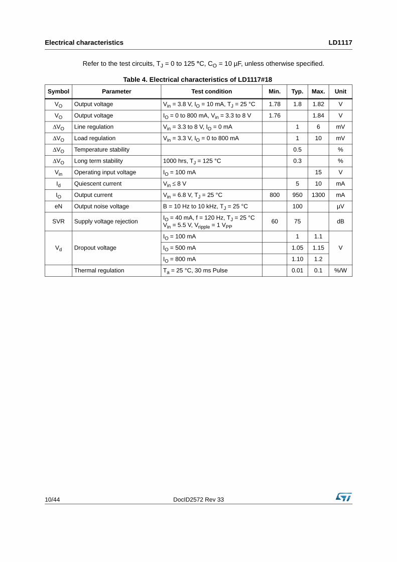
Refer to the test circuits, TJ = 0 to 125 °C, CO = 10 µF, unless otherwise specified.
Table 4. Electrical characteristics of LD1117#18
Symbol Parameter Test condition Min. Typ. Max. Unit
VO Output voltage Vin = 3.8 V, IO = 10 mA, TJ = 25 °C 1.78 1.8 1.82 V
VO Output voltage IO = 0 to 800 mA, Vin = 3.3 to 8 V 1.76 1.84 V
ΔVO Line regulation Vin = 3.3 to 8 V, IO = 0 mA 1 6 mV
ΔVO Load regulation Vin = 3.3 V, IO = 0 to 800 mA 1 10 mV
ΔVO Temperature stability 0.5 %
ΔVO Long term stability 1000 hrs, TJ = 125 °C 0.3 %
Vin Operating input voltage IO = 100 mA 15 V
Id Quiescent current Vin ≤ 8 V 5 10 mA
IO Output current Vin = 6.8 V, TJ = 25 °C 800 950 1300 mA
eN Output noise voltage B = 10 Hz to 10 kHz, TJ = 25 °C 100 µV
SVR Supply voltage rejectionIO = 40 mA, f = 120 Hz, TJ = 25 °C Vin = 5.5 V, Vripple = 1 VPP
60 75 dB
Vd Dropout voltage
IO = 100 mA 1 1.1
VIO = 500 mA 1.05 1.15
IO = 800 mA 1.10 1.2
Thermal regulation Ta = 25 °C, 30 ms Pulse 0.01 0.1 %/W
DocID2572 Rev 33 11/44
LD1117 Electrical characteristics
Refer to the test circuits, TJ = 0 to 125 °C, CO = 10 µF, unless otherwise specified.
Table 5. Electrical characteristics of LD1117#25
Symbol Parameter Test condition Min. Typ. Max. Unit
VO Output voltage Vin = 4.5 V, IO = 10 mA, TJ = 25 °C 2.475 2.5 2.525 V
VO Output voltage IO = 0 to 800 mA, Vin = 3.9 to 10 V 2.45 2.55 V
ΔVO Line regulation Vin = 3.9 to 10 V, IO = 0 mA 1 6 mV
ΔVO Load regulation Vin = 3.9 V, IO = 0 to 800 mA 1 10 mV
ΔVO Temperature stability 0.5 %
ΔVO Long term stability 1000 hrs, TJ = 125 °C 0.3 %
Vin Operating input voltage IO = 100 mA 15 V
Id Quiescent current Vin ≤ 10 V 5 10 mA
IO Output current Vin = 7.5 V TJ = 25 °C 800 950 1300 mA
eN Output noise voltage B = 10 Hz to 10 kHz, TJ = 25 °C 100 µV
SVR Supply voltage rejectionIO = 40 mA, f = 120 Hz, TJ = 25 °C Vin = 5.5 V, Vripple = 1 VPP
60 75 dB
Vd Dropout voltage
IO = 100 mA 1 1.1
VIO = 500 mA 1.05 1.15
IO = 800 mA 1.10 1.2
Thermal regulation Ta = 25 °C, 30 ms Pulse 0.01 0.1 %/W
Electrical characteristics LD1117
12/44 DocID2572 Rev 33
Refer to the test circuits, TJ = 0 to 125 °C, CO = 10 µF, unless otherwise specified.
Table 6. Electrical characteristics of LD1117#33
Symbol Parameter Test condition Min. Typ. Max. Unit
VO Output voltage Vin = 5.3 V, IO = 10 mA, TJ = 25 °C 3.267 3.3 3.333 V
VO Output voltage IO = 0 to 800 mA, Vin = 4.75 to 10 V 3.235 3.365 V
ΔVO Line regulation Vin = 4.75 to 15 V, IO = 0 mA 1 6 mV
ΔVO Load regulation Vin = 4.75 V, IO = 0 to 800 mA 1 10 mV
ΔVO Temperature stability 0.5 %
ΔVO Long term stability 1000 hrs, TJ = 125 °C 0.3 %
Vin Operating input voltage IO = 100 mA 15 V
Id Quiescent current Vin ≤ 15 V 5 10 mA
IO Output current Vin = 8.3 V, TJ = 25 °C 800 950 1300 mA
eN Output noise voltage B = 10 Hz to 10 kHz, TJ = 25 °C 100 µV
SVR Supply voltage rejectionIO = 40 mA, f = 120 Hz, TJ = 25 °C Vin = 6.3 V, Vripple = 1 VPP
60 75 dB
Vd Dropout voltage
IO = 100 mA 1 1.1
VIO = 500 mA 1.05 1.15
IO = 800 mA 1.10 1.2
Thermal regulation Ta = 25 °C, 30 ms Pulse 0.01 0.1 %/W

DocID2572 Rev 33 13/44
LD1117 Electrical characteristics
Refer to the test circuits, TJ = 0 to 125 °C, CO = 10 µF, unless otherwise specified.
Table 7. Electrical characteristics of LD1117#50
Symbol Parameter Test condition Min. Typ. Max. Unit
VO Output voltage Vin = 7 V, IO = 10 mA, TJ = 25 °C 4.95 5 5.05 V
VO Output voltage IO = 0 to 800 mA, Vin = 6.5 to 15 V 4.9 5.1 V
ΔVO Line regulation Vin = 6.5 to 15 V, IO = 0 mA 1 10 mV
ΔVO Load regulation Vin = 6.5 V, IO = 0 to 800 mA 1 15 mV
ΔVO Temperature stability 0.5 %
ΔVO Long term stability 1000 hrs, TJ = 125 °C 0.3 %
Vin Operating input voltage IO = 100 mA 15 V
Id Quiescent current Vin ≤ 15 V 5 10 mA
IO Output current Vin = 10 V, TJ = 25 °C 800 950 1300 mA
eN Output noise voltage B = 10 Hz to 10 kHz, TJ = 25 °C 100 µV
SVR Supply voltage rejectionIO = 40 mA, f = 120 Hz, TJ = 25 °C Vin = 8 V, Vripple = 1 VPP
60 75 dB
Vd Dropout voltage
IO = 100 mA 1 1.1
VIO = 500 mA 1.05 1.15
IO = 800 mA 1.10 1.2
Thermal regulation Ta = 25 °C, 30 ms Pulse 0.01 0.1 %/W
Electrical characteristics LD1117
14/44 DocID2572 Rev 33
Refer to the test circuits, TJ = 0 to 125 °C, CO = 10 µF, unless otherwise specified.
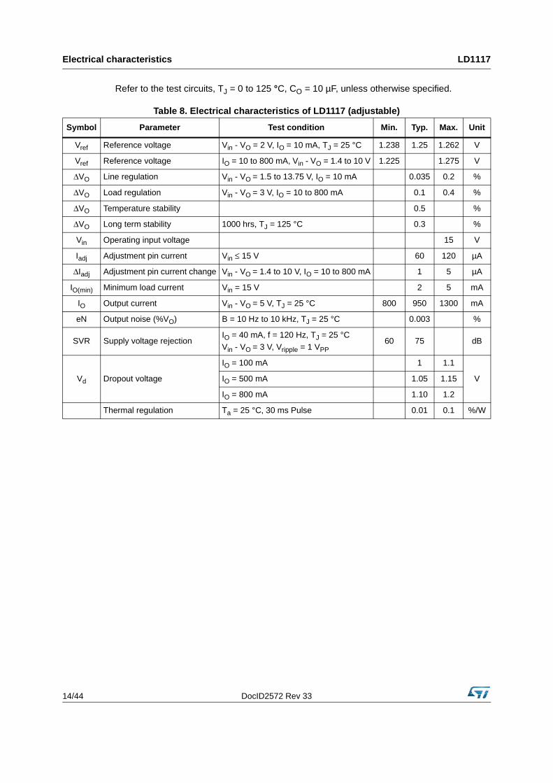
Table 8. Electrical characteristics of LD1117 (adjustable)
Symbol Parameter Test condition Min. Typ. Max. Unit
Vref Reference voltage Vin - VO = 2 V, IO = 10 mA, TJ = 25 °C 1.238 1.25 1.262 V
Vref Reference voltage IO = 10 to 800 mA, Vin - VO = 1.4 to 10 V 1.225 1.275 V
ΔVO Line regulation Vin - VO = 1.5 to 13.75 V, IO = 10 mA 0.035 0.2 %
ΔVO Load regulation Vin - VO = 3 V, IO = 10 to 800 mA 0.1 0.4 %
ΔVO Temperature stability 0.5 %
ΔVO Long term stability 1000 hrs, TJ = 125 °C 0.3 %
Vin Operating input voltage 15 V
Iadj Adjustment pin current Vin ≤ 15 V 60 120 µA
ΔIadj Adjustment pin current change Vin - VO = 1.4 to 10 V, IO = 10 to 800 mA 1 5 µA
IO(min) Minimum load current Vin = 15 V 2 5 mA
IO Output current Vin - VO = 5 V, TJ = 25 °C 800 950 1300 mA
eN Output noise (%VO) B = 10 Hz to 10 kHz, TJ = 25 °C 0.003 %
SVR Supply voltage rejectionIO = 40 mA, f = 120 Hz, TJ = 25 °CVin - VO = 3 V, Vripple = 1 VPP
60 75 dB
Vd Dropout voltage
IO = 100 mA 1 1.1
VIO = 500 mA 1.05 1.15
IO = 800 mA 1.10 1.2
Thermal regulation Ta = 25 °C, 30 ms Pulse 0.01 0.1 %/W
DocID2572 Rev 33 15/44
LD1117 Electrical characteristics
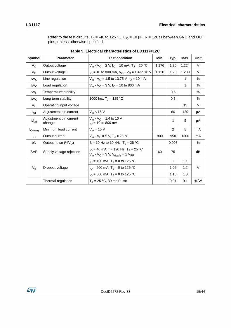
Refer to the test circuits, TJ = -40 to 125 °C, CO = 10 µF, R = 120 Ω between GND and OUT pins, unless otherwise specified.
Table 9. Electrical characteristics of LD1117#12C
Symbol Parameter Test condition Min. Typ. Max. Unit
VO Output voltage Vin - VO = 2 V, IO = 10 mA, TJ = 25 °C 1.176 1.20 1.224 V
VO Output voltage IO = 10 to 800 mA, Vin - VO = 1.4 to 10 V 1.120 1.20 1.280 V
ΔVO Line regulation Vin - VO = 1.5 to 13.75 V, IO = 10 mA 1 %
ΔVO Load regulation Vin - VO = 3 V, IO = 10 to 800 mA 1 %
ΔVO Temperature stability 0.5 %
ΔVO Long term stability 1000 hrs, TJ = 125 °C 0.3 %
Vin Operating input voltage 15 V
Iadj Adjustment pin current Vin ≤ 15 V 60 120 µA
ΔIadjAdjustment pin current change
Vin - VO = 1.4 to 10 VIO = 10 to 800 mA
1 5 µA
IO(min) Minimum load current Vin = 15 V 2 5 mA
IO Output current Vin - VO = 5 V, TJ = 25 °C 800 950 1300 mA
eN Output noise (%VO) B = 10 Hz to 10 kHz, TJ = 25 °C 0.003 %
SVR Supply voltage rejectionIO = 40 mA, f = 120 Hz, TJ = 25 °CVin - VO = 3 V, Vripple = 1 VPP
60 75 dB
Vd Dropout voltage
IO = 100 mA, TJ = 0 to 125 °C 1 1.1
VIO = 500 mA, TJ = 0 to 125 °C 1.05 1.2
IO = 800 mA, TJ = 0 to 125 °C 1.10 1.3
Thermal regulation Ta = 25 °C, 30 ms Pulse 0.01 0.1 %/W
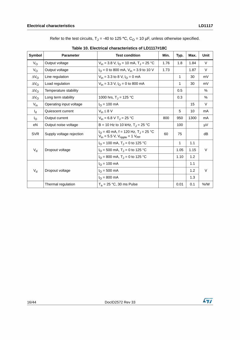
Electrical characteristics LD1117
16/44 DocID2572 Rev 33
Refer to the test circuits, TJ = -40 to 125 °C, CO = 10 µF, unless otherwise specified.
Table 10. Electrical characteristics of LD1117#18C
Symbol Parameter Test condition Min. Typ. Max. Unit
VO Output voltage Vin = 3.8 V, IO = 10 mA, TJ = 25 °C 1.76 1.8 1.84 V
VO Output voltage IO = 0 to 800 mA, Vin = 3.9 to 10 V 1.73 1.87 V
ΔVO Line regulation Vin = 3.3 to 8 V, IO = 0 mA 1 30 mV
ΔVO Load regulation Vin = 3.3 V, IO = 0 to 800 mA 1 30 mV
ΔVO Temperature stability 0.5 %
ΔVO Long term stability 1000 hrs, TJ = 125 °C 0.3 %
Vin Operating input voltage IO = 100 mA 15 V
Id Quiescent current Vin ≤ 8 V 5 10 mA
IO Output current Vin = 6.8 V TJ = 25 °C 800 950 1300 mA
eN Output noise voltage B = 10 Hz to 10 kHz, TJ = 25 °C 100 µV
SVR Supply voltage rejectionIO = 40 mA, f = 120 Hz, TJ = 25 °C Vin = 5.5 V, Vripple = 1 VPP
60 75 dB
Vd Dropout voltage
IO = 100 mA, TJ = 0 to 125 °C 1 1.1
VIO = 500 mA, TJ = 0 to 125 °C 1.05 1.15
IO = 800 mA, TJ = 0 to 125 °C 1.10 1.2
Vd Dropout voltage
IO = 100 mA 1.1
VIO = 500 mA 1.2
IO = 800 mA 1.3
Thermal regulation Ta = 25 °C, 30 ms Pulse 0.01 0.1 %/W
DocID2572 Rev 33 17/44
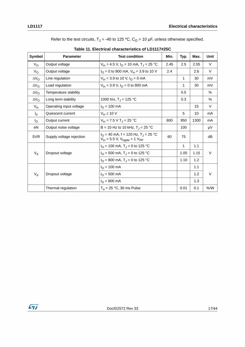
LD1117 Electrical characteristics
Refer to the test circuits, TJ = -40 to 125 °C, CO = 10 µF, unless otherwise specified.
Table 11. Electrical characteristics of LD1117#25C
Symbol Parameter Test condition Min. Typ. Max. Unit
VO Output voltage Vin = 4.5 V, IO = 10 mA, TJ = 25 °C 2.45 2.5 2.55 V
VO Output voltage IO = 0 to 800 mA, Vin = 3.9 to 10 V 2.4 2.6 V
ΔVO Line regulation Vin = 3.9 to 10 V, IO = 0 mA 1 30 mV
ΔVO Load regulation Vin = 3.9 V, IO = 0 to 800 mA 1 30 mV
ΔVO Temperature stability 0.5 %
ΔVO Long term stability 1000 hrs, TJ = 125 °C 0.3 %
Vin Operating input voltage IO = 100 mA 15 V
Id Quiescent current Vin ≤ 10 V 5 10 mA
IO Output current Vin = 7.5 V TJ = 25 °C 800 950 1300 mA
eN Output noise voltage B = 10 Hz to 10 kHz, TJ = 25 °C 100 µV
SVR Supply voltage rejectionIO = 40 mA, f = 120 Hz, TJ = 25 °C Vin = 5.5 V, Vripple = 1 VPP
60 75 dB
Vd Dropout voltage
IO = 100 mA, TJ = 0 to 125 °C 1 1.1
VIO = 500 mA, TJ = 0 to 125 °C 1.05 1.15
IO = 800 mA, TJ = 0 to 125 °C 1.10 1.2
Vd Dropout voltage
IO = 100 mA 1.1
VIO = 500 mA 1.2
IO = 800 mA 1.3
Thermal regulation Ta = 25 °C, 30 ms Pulse 0.01 0.1 %/W
Electrical characteristics LD1117
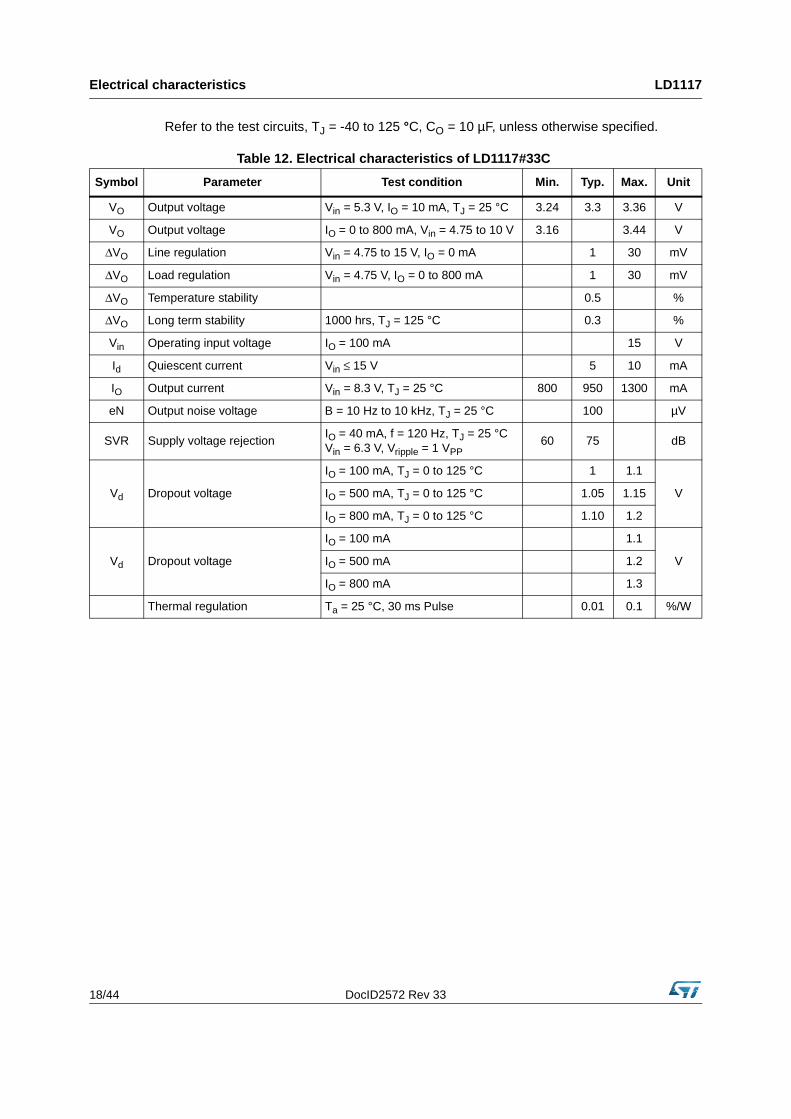
18/44 DocID2572 Rev 33
Refer to the test circuits, TJ = -40 to 125 °C, CO = 10 µF, unless otherwise specified.
Table 12. Electrical characteristics of LD1117#33C
Symbol Parameter Test condition Min. Typ. Max. Unit
VO Output voltage Vin = 5.3 V, IO = 10 mA, TJ = 25 °C 3.24 3.3 3.36 V
VO Output voltage IO = 0 to 800 mA, Vin = 4.75 to 10 V 3.16 3.44 V
ΔVO Line regulation Vin = 4.75 to 15 V, IO = 0 mA 1 30 mV
ΔVO Load regulation Vin = 4.75 V, IO = 0 to 800 mA 1 30 mV
ΔVO Temperature stability 0.5 %
ΔVO Long term stability 1000 hrs, TJ = 125 °C 0.3 %
Vin Operating input voltage IO = 100 mA 15 V
Id Quiescent current Vin ≤ 15 V 5 10 mA
IO Output current Vin = 8.3 V, TJ = 25 °C 800 950 1300 mA
eN Output noise voltage B = 10 Hz to 10 kHz, TJ = 25 °C 100 µV
SVR Supply voltage rejectionIO = 40 mA, f = 120 Hz, TJ = 25 °C Vin = 6.3 V, Vripple = 1 VPP
60 75 dB
Vd Dropout voltage
IO = 100 mA, TJ = 0 to 125 °C 1 1.1
VIO = 500 mA, TJ = 0 to 125 °C 1.05 1.15
IO = 800 mA, TJ = 0 to 125 °C 1.10 1.2
Vd Dropout voltage
IO = 100 mA 1.1
VIO = 500 mA 1.2
IO = 800 mA 1.3
Thermal regulation Ta = 25 °C, 30 ms Pulse 0.01 0.1 %/W
DocID2572 Rev 33 19/44
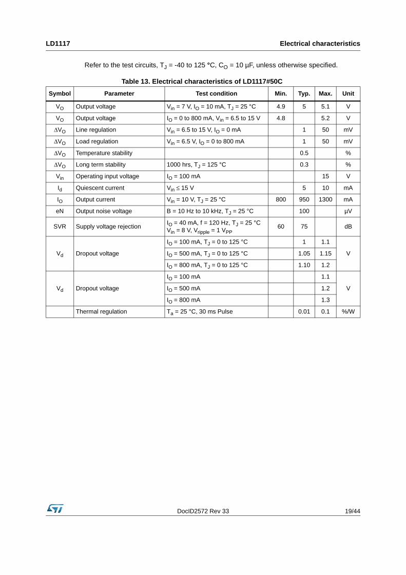
LD1117 Electrical characteristics
Refer to the test circuits, TJ = -40 to 125 °C, CO = 10 µF, unless otherwise specified.
Table 13. Electrical characteristics of LD1117#50C
Symbol Parameter Test condition Min. Typ. Max. Unit
VO Output voltage Vin = 7 V, IO = 10 mA, TJ = 25 °C 4.9 5 5.1 V
VO Output voltage IO = 0 to 800 mA, Vin = 6.5 to 15 V 4.8 5.2 V
ΔVO Line regulation Vin = 6.5 to 15 V, IO = 0 mA 1 50 mV
ΔVO Load regulation Vin = 6.5 V, IO = 0 to 800 mA 1 50 mV
ΔVO Temperature stability 0.5 %
ΔVO Long term stability 1000 hrs, TJ = 125 °C 0.3 %
Vin Operating input voltage IO = 100 mA 15 V
Id Quiescent current Vin ≤ 15 V 5 10 mA
IO Output current Vin = 10 V, TJ = 25 °C 800 950 1300 mA
eN Output noise voltage B = 10 Hz to 10 kHz, TJ = 25 °C 100 µV
SVR Supply voltage rejectionIO = 40 mA, f = 120 Hz, TJ = 25 °C Vin = 8 V, Vripple = 1 VPP
60 75 dB
Vd Dropout voltage
IO = 100 mA, TJ = 0 to 125 °C 1 1.1
VIO = 500 mA, TJ = 0 to 125 °C 1.05 1.15
IO = 800 mA, TJ = 0 to 125 °C 1.10 1.2
Vd Dropout voltage
IO = 100 mA 1.1
VIO = 500 mA 1.2
IO = 800 mA 1.3
Thermal regulation Ta = 25 °C, 30 ms Pulse 0.01 0.1 %/W
Electrical characteristics LD1117
20/44 DocID2572 Rev 33
Refer to the test circuits, TJ = -40 to 125 °C, CO = 10 µF, unless otherwise specified.
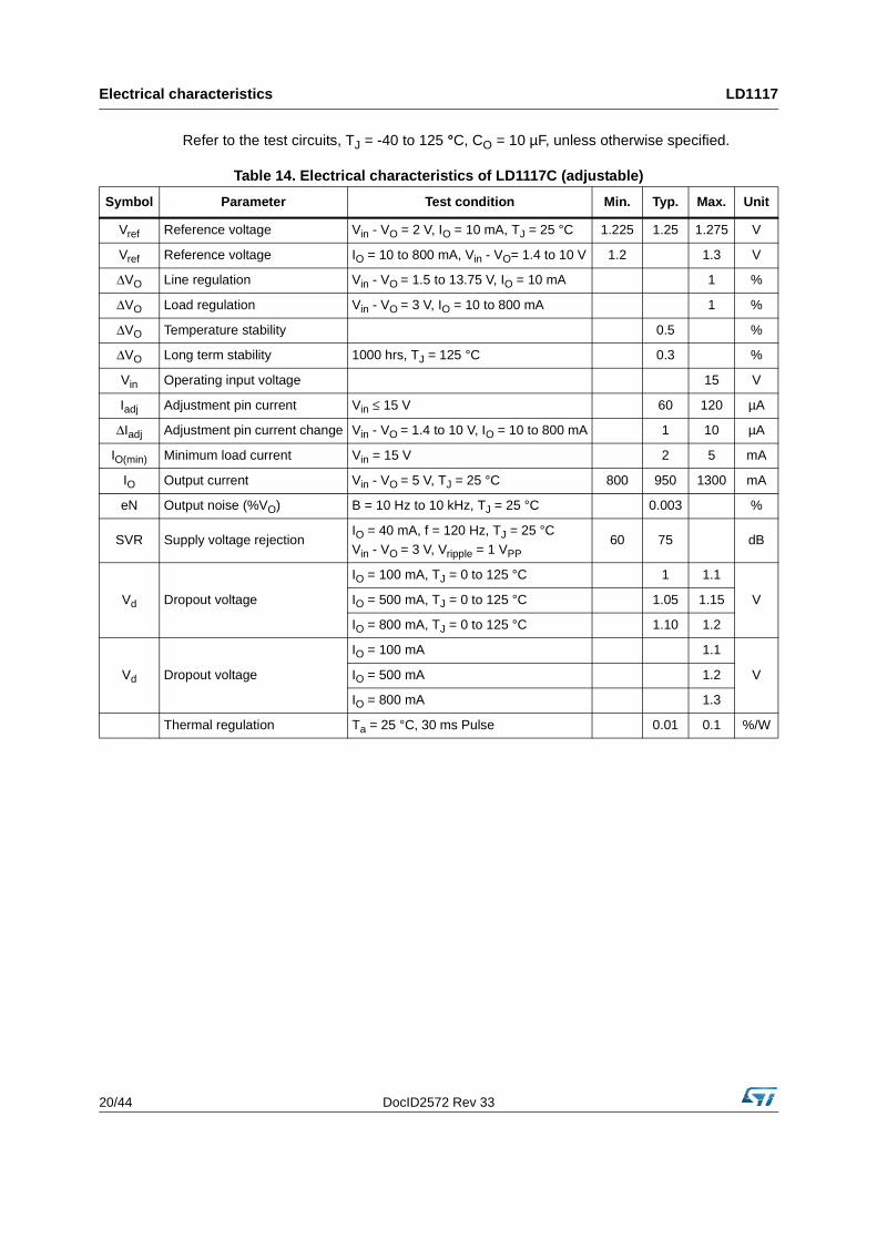
Table 14. Electrical characteristics of LD1117C (adjustable)
Symbol Parameter Test condition Min. Typ. Max. Unit
Vref Reference voltage Vin - VO = 2 V, IO = 10 mA, TJ = 25 °C 1.225 1.25 1.275 V
Vref Reference voltage IO = 10 to 800 mA, Vin - VO= 1.4 to 10 V 1.2 1.3 V
ΔVO Line regulation Vin - VO = 1.5 to 13.75 V, IO = 10 mA 1 %
ΔVO Load regulation Vin - VO = 3 V, IO = 10 to 800 mA 1 %
ΔVO Temperature stability 0.5 %
ΔVO Long term stability 1000 hrs, TJ = 125 °C 0.3 %
Vin Operating input voltage 15 V
Iadj Adjustment pin current Vin ≤ 15 V 60 120 µA
ΔIadj Adjustment pin current change Vin - VO = 1.4 to 10 V, IO = 10 to 800 mA 1 10 µA
IO(min) Minimum load current Vin = 15 V 2 5 mA
IO Output current Vin - VO = 5 V, TJ = 25 °C 800 950 1300 mA
eN Output noise (%VO) B = 10 Hz to 10 kHz, TJ = 25 °C 0.003 %
SVR Supply voltage rejectionIO = 40 mA, f = 120 Hz, TJ = 25 °CVin - VO = 3 V, Vripple = 1 VPP
60 75 dB
Vd Dropout voltage
IO = 100 mA, TJ = 0 to 125 °C 1 1.1
VIO = 500 mA, TJ = 0 to 125 °C 1.05 1.15
IO = 800 mA, TJ = 0 to 125 °C 1.10 1.2
Vd Dropout voltage
IO = 100 mA 1.1
VIO = 500 mA 1.2
IO = 800 mA 1.3
Thermal regulation Ta = 25 °C, 30 ms Pulse 0.01 0.1 %/W
DocID2572 Rev 33 21/44
LD1117 Typical application
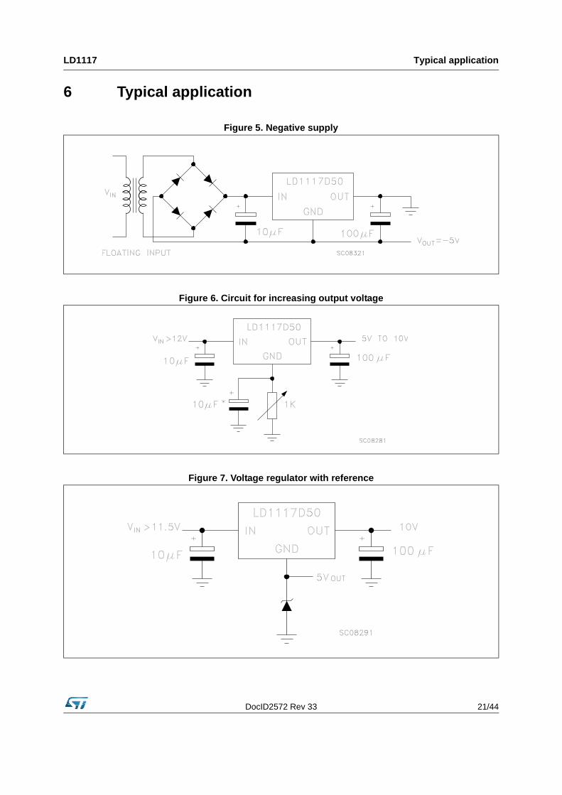
6 Typical application
Figure 5. Negative supply
Figure 6. Circuit for increasing output voltage
Figure 7. Voltage regulator with reference
Typical application LD1117
22/44 DocID2572 Rev 33
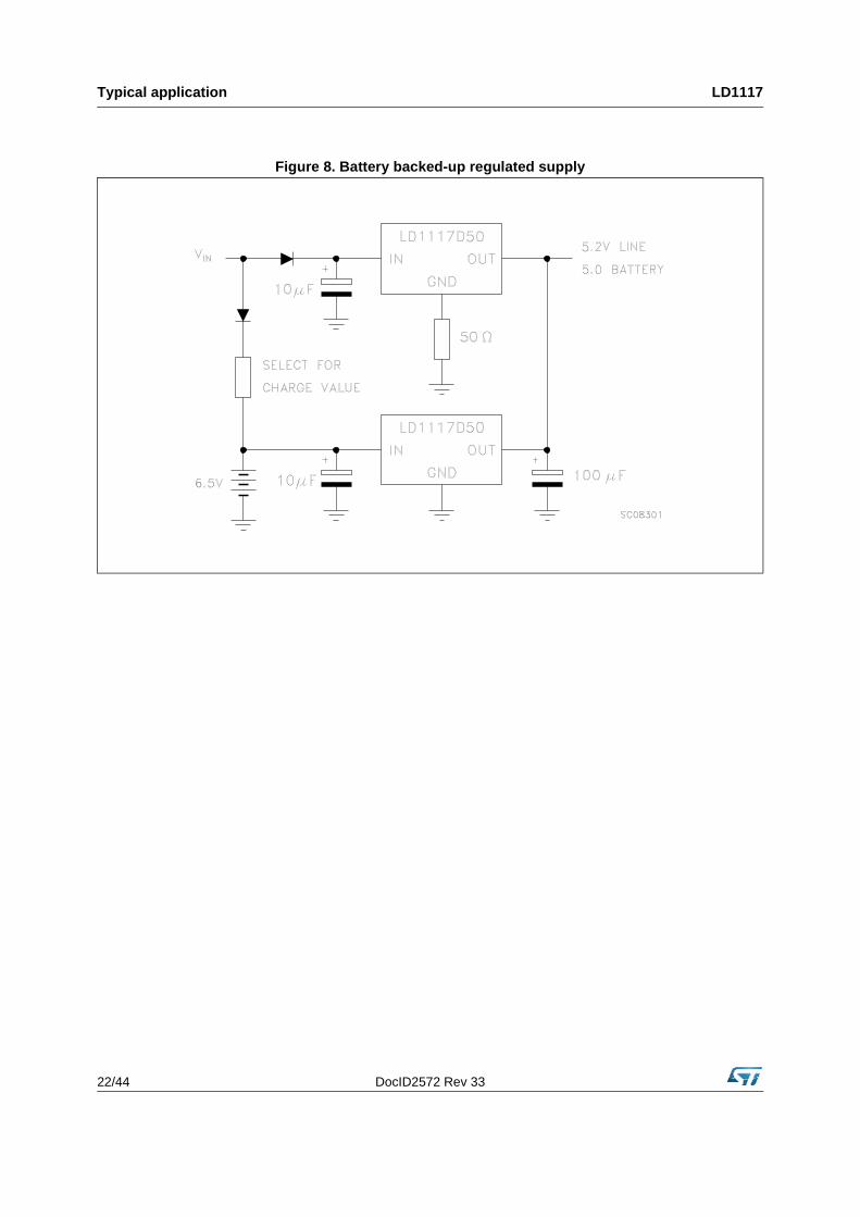
Figure 8. Battery backed-up regulated supply
DocID2572 Rev 33 23/44
LD1117 Typical application
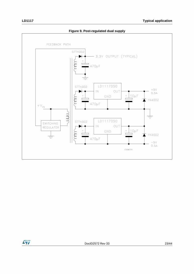
Figure 9. Post-regulated dual supply
LD1117 adjustable: application note LD1117
24/44 DocID2572 Rev 33
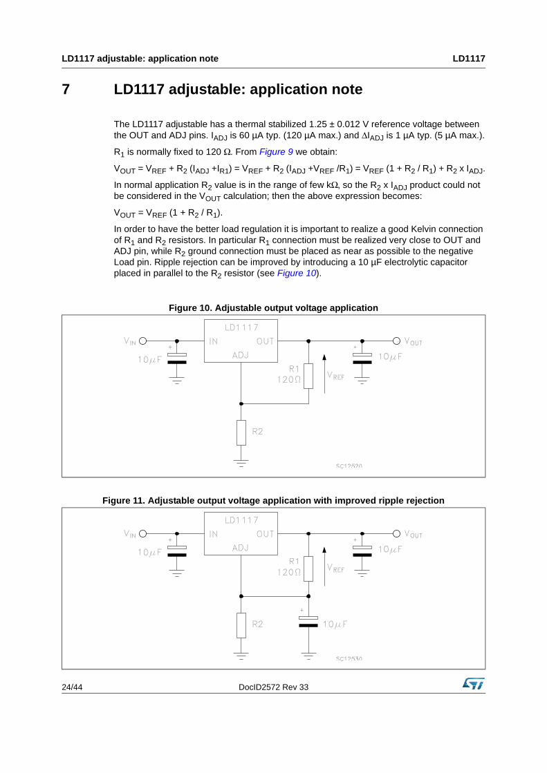
7 LD1117 adjustable: application note
The LD1117 adjustable has a thermal stabilized 1.25 ± 0.012 V reference voltage between the OUT and ADJ pins. IADJ is 60 µA typ. (120 µA max.) and ΔIADJ is 1 µA typ. (5 µA max.).
R1 is normally fixed to 120 Ω. From Figure 9 we obtain:
VOUT = VREF + R2 (IADJ +IR1) = VREF + R2 (IADJ +VREF /R1) = VREF (1 + R2 / R1) + R2 x IADJ.
In normal application R2 value is in the range of few kΩ, so the R2 x IADJ product could not be considered in the VOUT calculation; then the above expression becomes:
VOUT = VREF (1 + R2 / R1).
In order to have the better load regulation it is important to realize a good Kelvin connection of R1 and R2 resistors. In particular R1 connection must be realized very close to OUT and ADJ pin, while R2 ground connection must be placed as near as possible to the negative Load pin. Ripple rejection can be improved by introducing a 10 µF electrolytic capacitor placed in parallel to the R2 resistor (see Figure 10).
Figure 10. Adjustable output voltage application
Figure 11. Adjustable output voltage application with improved ripple rejection
DocID2572 Rev 33 25/44
LD1117 Package mechanical data
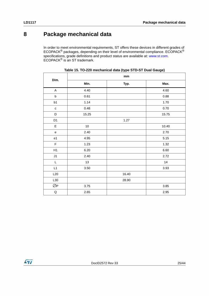
8 Package mechanical data
In order to meet environmental requirements, ST offers these devices in different grades of ECOPACK® packages, depending on their level of environmental compliance. ECOPACK® specifications, grade definitions and product status are available at: www.st.com. ECOPACK® is an ST trademark.
Table 15. TO-220 mechanical data (type STD-ST Dual Gauge)
Dim.mm
Min. Typ. Max.
A 4.40 4.60
b 0.61 0.88
b1 1.14 1.70
c 0.48 0.70
D 15.25 15.75
D1 1.27
E 10 10.40
e 2.40 2.70
e1 4.95 5.15
F 1.23 1.32
H1 6.20 6.60
J1 2.40 2.72
L 13 14
L1 3.50 3.93
L20 16.40
L30 28.90
∅P 3.75 3.85
Q 2.65 2.95
Package mechanical data LD1117
26/44 DocID2572 Rev 33
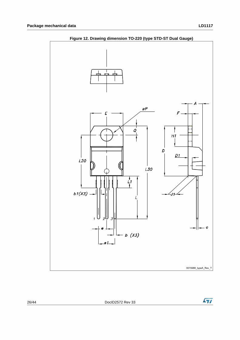
Figure 12. Drawing dimension TO-220 (type STD-ST Dual Gauge)
DocID2572 Rev 33 27/44
LD1117 Package mechanical data
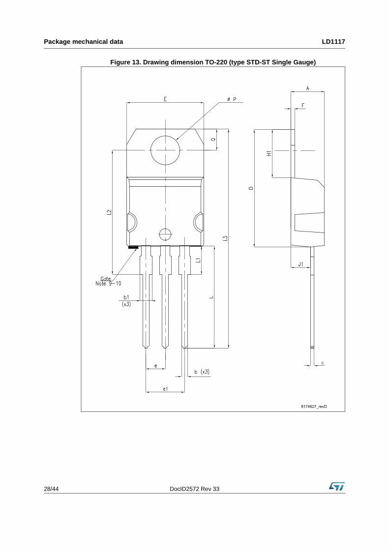
Table 16. TO-220 mechanical data (type STD-ST Single Gauge)
Dim.mm
Min. Typ. Max.
A 4.40 4.60
b 0.61 0.88
b1 1.14 1.70
c 0.48 0.70
D 15.25 15.75
E 10 10.40
e 2.40 2.70
e1 4.95 5.15
F 0.51 0.60
H1 6.20 6.60
J1 2.40 2.72
L 13 14
L1 3.50 3.93
L20 16.40
L30 28.90
∅P 3.75 3.85
Q 2.65 2.95
Package mechanical data LD1117
28/44 DocID2572 Rev 33
Figure 13. Drawing dimension TO-220 (type STD-ST Single Gauge)
DocID2572 Rev 33 29/44
LD1117 Package mechanical data
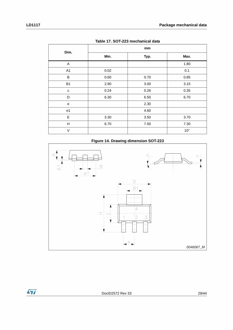
Figure 14. Drawing dimension SOT-223
Table 17. SOT-223 mechanical data
Dim.mm
Min. Typ. Max.
A 1.80
A1 0.02 0.1
B 0.60 0.70 0.85
B1 2.90 3.00 3.15
c 0.24 0.26 0.35
D 6.30 6.50 6.70
e 2.30
e1 4.60
E 3.30 3.50 3.70
H 6.70 7.00 7.30
V 10°
0046067_M
Package mechanical data LD1117
30/44 DocID2572 Rev 33
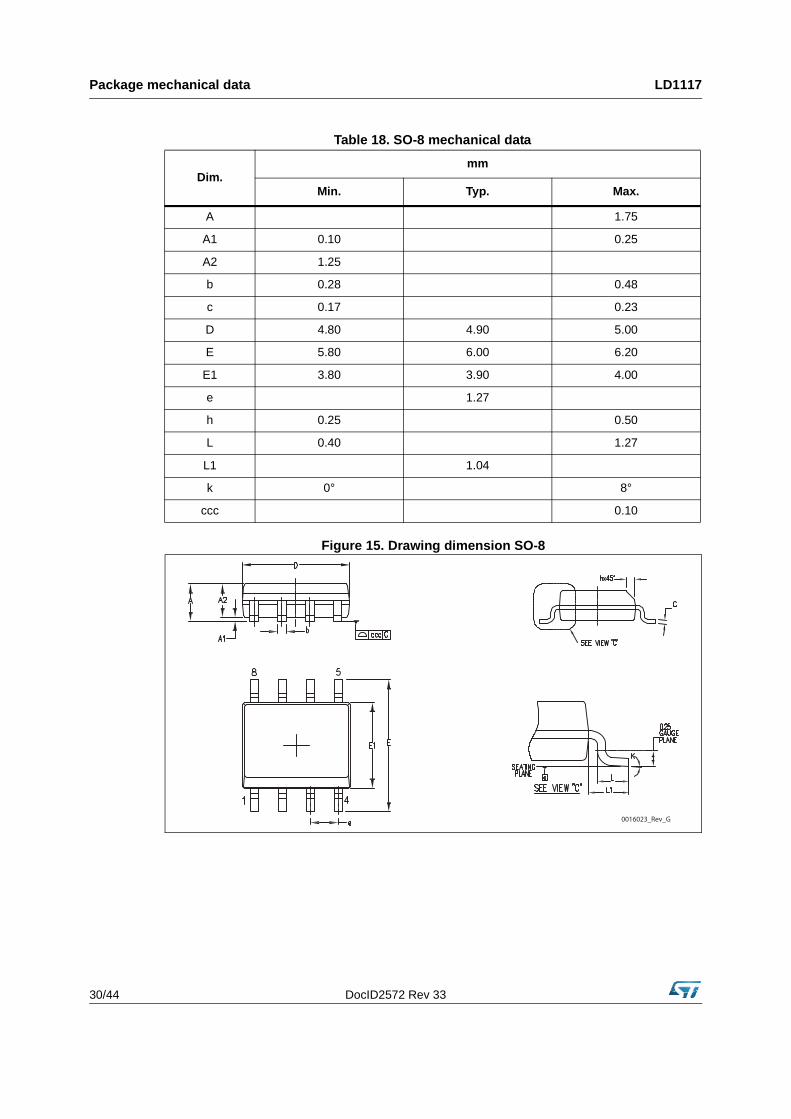
Figure 15. Drawing dimension SO-8
Table 18. SO-8 mechanical data
Dim.mm
Min. Typ. Max.
A 1.75
A1 0.10 0.25
A2 1.25
b 0.28 0.48
c 0.17 0.23
D 4.80 4.90 5.00
E 5.80 6.00 6.20
E1 3.80 3.90 4.00
e 1.27
h 0.25 0.50
L 0.40 1.27
L1 1.04
k 0° 8°
ccc 0.10
0016023_Rev_G
DocID2572 Rev 33 31/44
LD1117 Package mechanical data
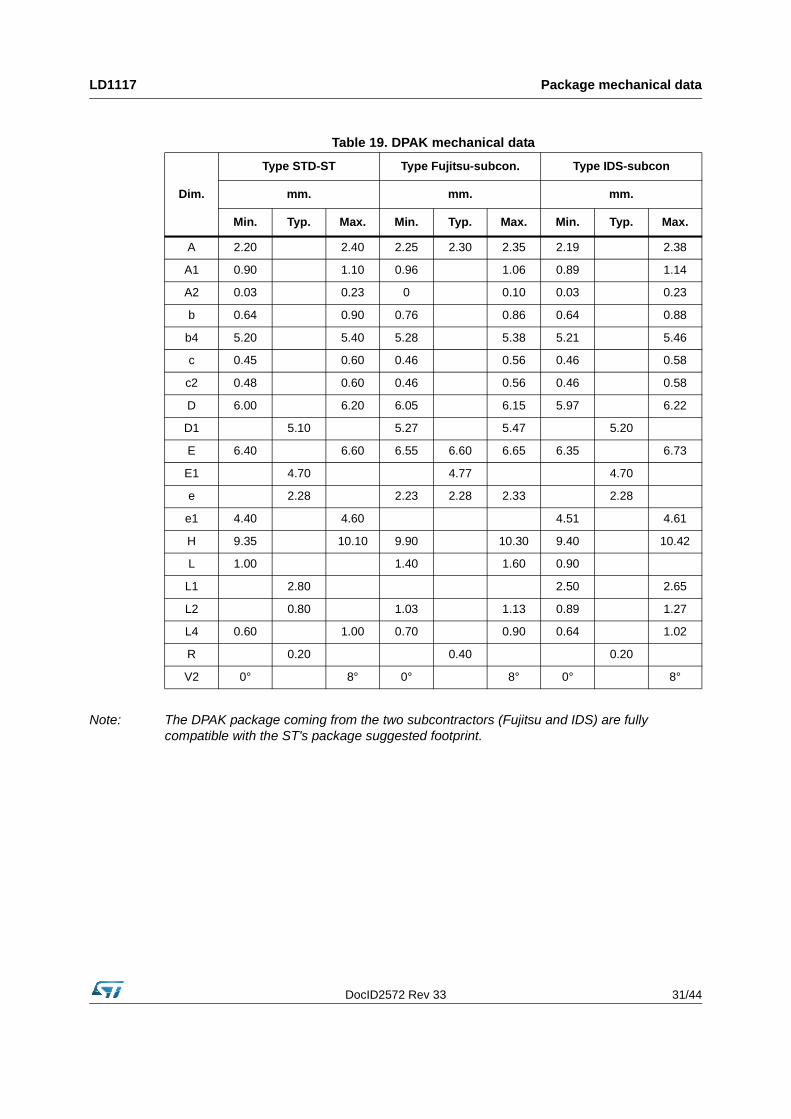
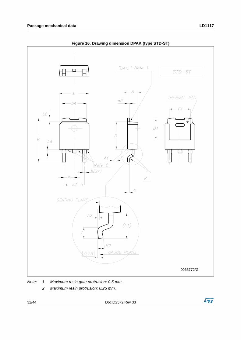
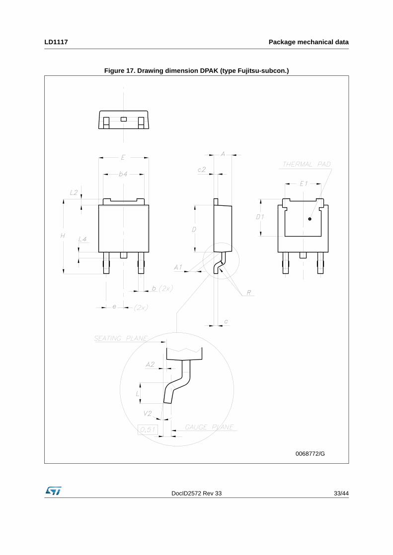
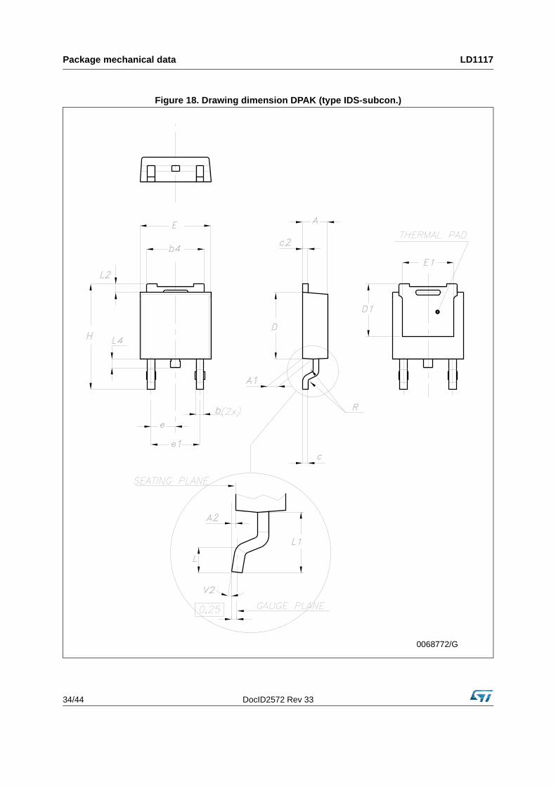
Note: The DPAK package coming from the two subcontractors (Fujitsu and IDS) are fully compatible with the ST's package suggested footprint.
Table 19. DPAK mechanical data
Dim.
Type STD-ST Type Fujitsu-subcon. Type IDS-subcon
mm. mm. mm.
Min. Typ. Max. Min. Typ. Max. Min. Typ. Max.
A 2.20 2.40 2.25 2.30 2.35 2.19 2.38
A1 0.90 1.10 0.96 1.06 0.89 1.14
A2 0.03 0.23 0 0.10 0.03 0.23
b 0.64 0.90 0.76 0.86 0.64 0.88
b4 5.20 5.40 5.28 5.38 5.21 5.46
c 0.45 0.60 0.46 0.56 0.46 0.58
c2 0.48 0.60 0.46 0.56 0.46 0.58
D 6.00 6.20 6.05 6.15 5.97 6.22
D1 5.10 5.27 5.47 5.20
E 6.40 6.60 6.55 6.60 6.65 6.35 6.73
E1 4.70 4.77 4.70
e 2.28 2.23 2.28 2.33 2.28
e1 4.40 4.60 4.51 4.61
H 9.35 10.10 9.90 10.30 9.40 10.42
L 1.00 1.40 1.60 0.90
L1 2.80 2.50 2.65
L2 0.80 1.03 1.13 0.89 1.27
L4 0.60 1.00 0.70 0.90 0.64 1.02
R 0.20 0.40 0.20
V2 0° 8° 0° 8° 0° 8°
Package mechanical data LD1117
32/44 DocID2572 Rev 33
Note: 1 Maximum resin gate protrusion: 0.5 mm.
2 Maximum resin protrusion: 0.25 mm.
Figure 16. Drawing dimension DPAK (type STD-ST)
0068772/G
DocID2572 Rev 33 33/44
LD1117 Package mechanical data
Figure 17. Drawing dimension DPAK (type Fujitsu-subcon.)
0068772/G
Package mechanical data LD1117
34/44 DocID2572 Rev 33
Figure 18. Drawing dimension DPAK (type IDS-subcon.)
0068772/G
DocID2572 Rev 33 35/44
LD1117 Package mechanical data
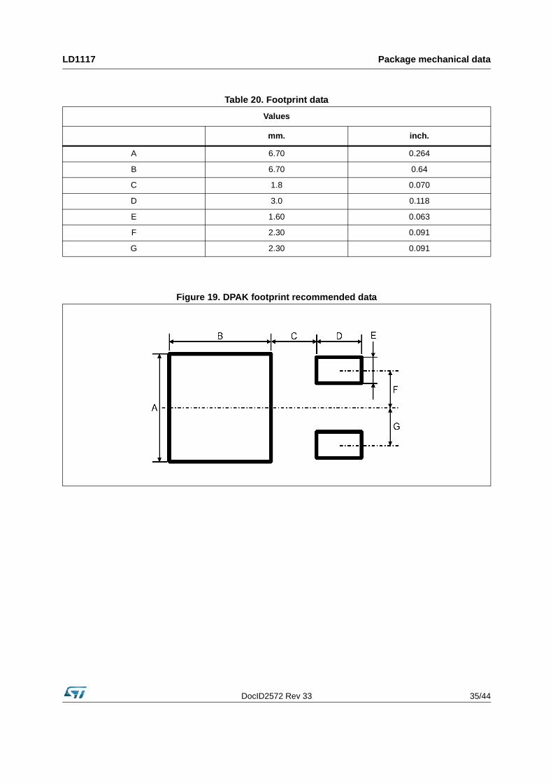
Table 20. Footprint data
Values
mm. inch.
A 6.70 0.264
B 6.70 0.64
C 1.8 0.070
D 3.0 0.118
E 1.60 0.063
F 2.30 0.091
G 2.30 0.091
Figure 19. DPAK footprint recommended data
Packaging mechanical data LD1117
36/44 DocID2572 Rev 33
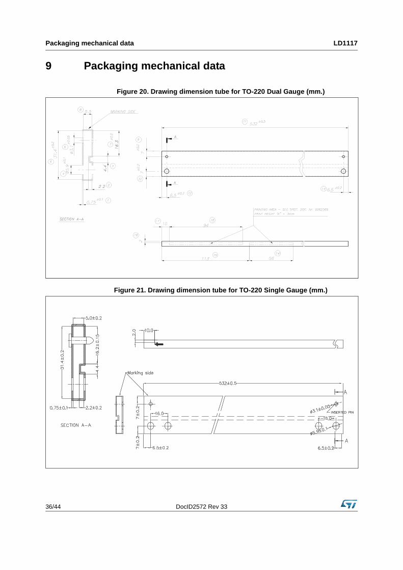
9 Packaging mechanical data
Figure 20. Drawing dimension tube for TO-220 Dual Gauge (mm.)
Figure 21. Drawing dimension tube for TO-220 Single Gauge (mm.)
DocID2572 Rev 33 37/44
LD1117 Packaging mechanical data
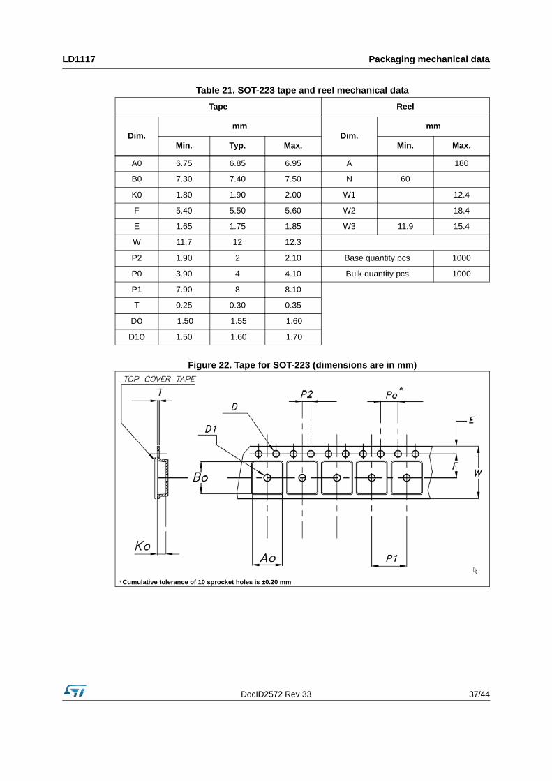
Figure 22. Tape for SOT-223 (dimensions are in mm)
Table 21. SOT-223 tape and reel mechanical data
Tape Reel
Dim.mm
Dim.mm
Min. Typ. Max. Min. Max.
A0 6.75 6.85 6.95 A 180
B0 7.30 7.40 7.50 N 60
K0 1.80 1.90 2.00 W1 12.4
F 5.40 5.50 5.60 W2 18.4
E 1.65 1.75 1.85 W3 11.9 15.4
W 11.7 12 12.3
P2 1.90 2 2.10 Base quantity pcs 1000
P0 3.90 4 4.10 Bulk quantity pcs 1000
P1 7.90 8 8.10
T 0.25 0.30 0.35
Dφ 1.50 1.55 1.60
D1φ 1.50 1.60 1.70
*Cumulative tolerance of 10 sprocket holes is ±0.20 mm
Packaging mechanical data LD1117
38/44 DocID2572 Rev 33
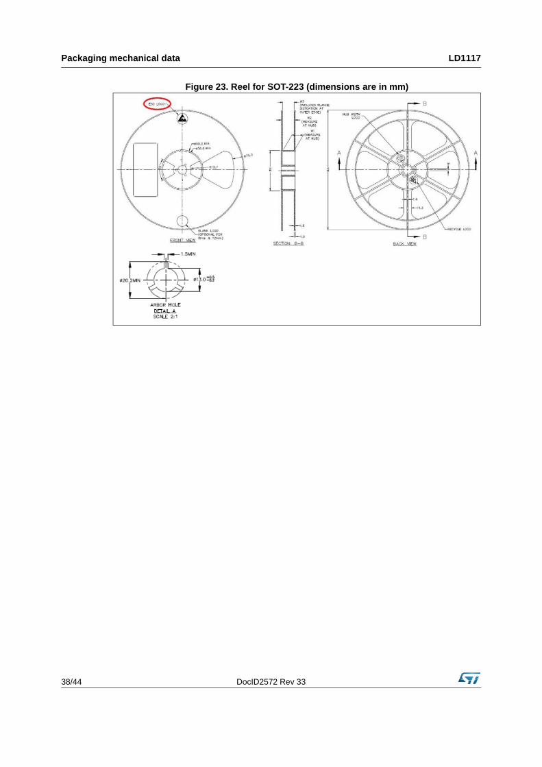
Figure 23. Reel for SOT-223 (dimensions are in mm)
DocID2572 Rev 33 39/44
LD1117 Packaging mechanical data
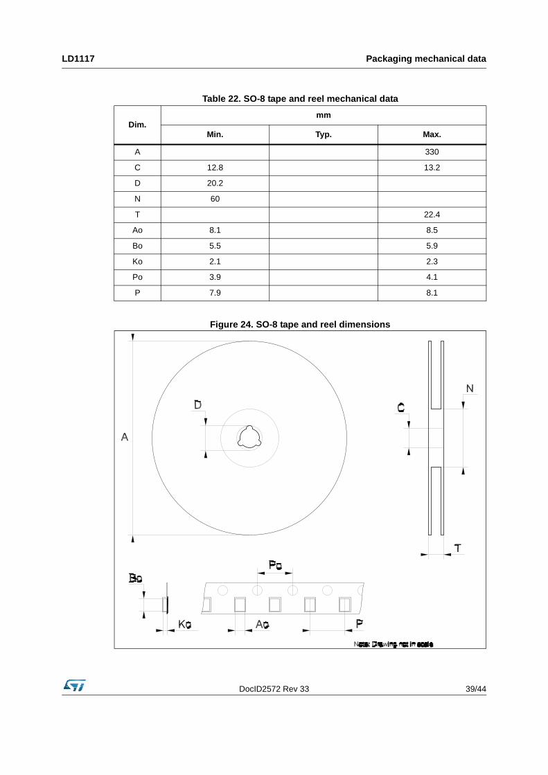
Figure 24. SO-8 tape and reel dimensions
Table 22. SO-8 tape and reel mechanical data
Dim.mm
Min. Typ. Max.
A 330
C 12.8 13.2
D 20.2
N 60
T 22.4
Ao 8.1 8.5
Bo 5.5 5.9
Ko 2.1 2.3
Po 3.9 4.1
P 7.9 8.1
Packaging mechanical data LD1117
40/44 DocID2572 Rev 33
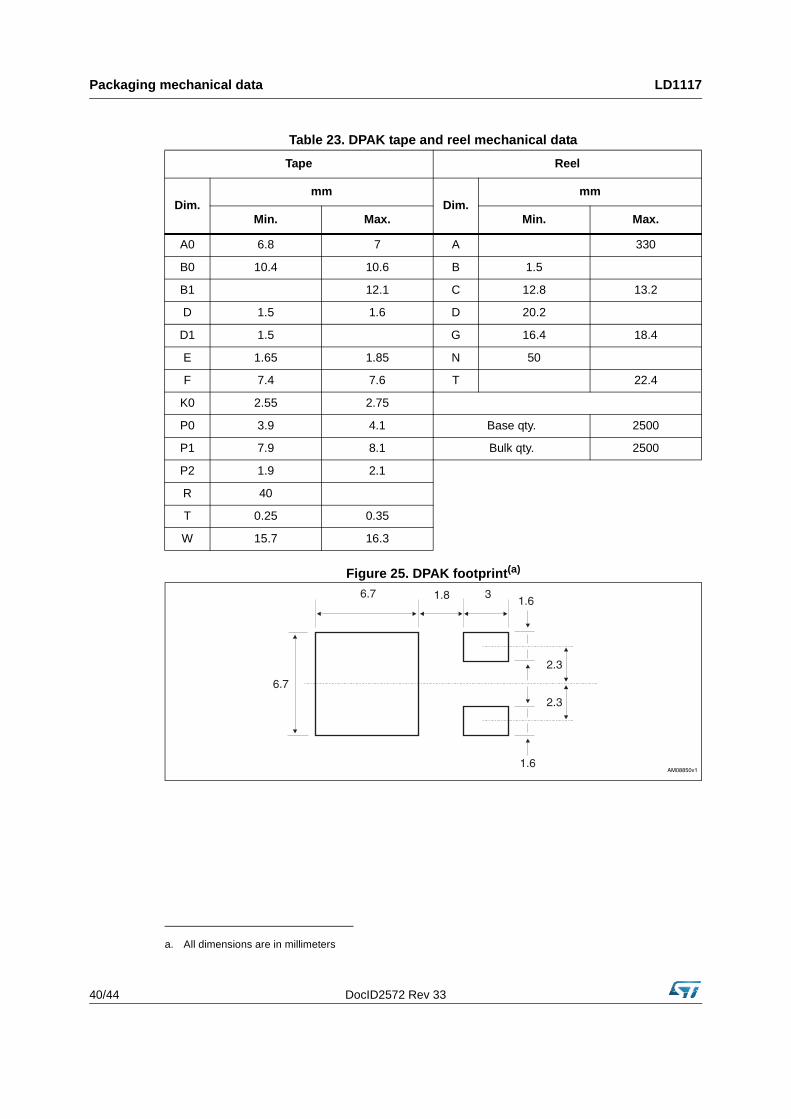
Figure 25. DPAK footprint(a)
Table 23. DPAK tape and reel mechanical data
Tape Reel
Dim.mm
Dim.mm
Min. Max. Min. Max.
A0 6.8 7 A 330
B0 10.4 10.6 B 1.5
B1 12.1 C 12.8 13.2
D 1.5 1.6 D 20.2
D1 1.5 G 16.4 18.4
E 1.65 1.85 N 50
F 7.4 7.6 T 22.4
K0 2.55 2.75
P0 3.9 4.1 Base qty. 2500
P1 7.9 8.1 Bulk qty. 2500
P2 1.9 2.1
R 40
T 0.25 0.35
W 15.7 16.3
a. All dimensions are in millimeters
6.7
1.6
1.6
2.3
2.3
6.7 1.8 3
AM08850v1
DocID2572 Rev 33 41/44
LD1117 Packaging mechanical data
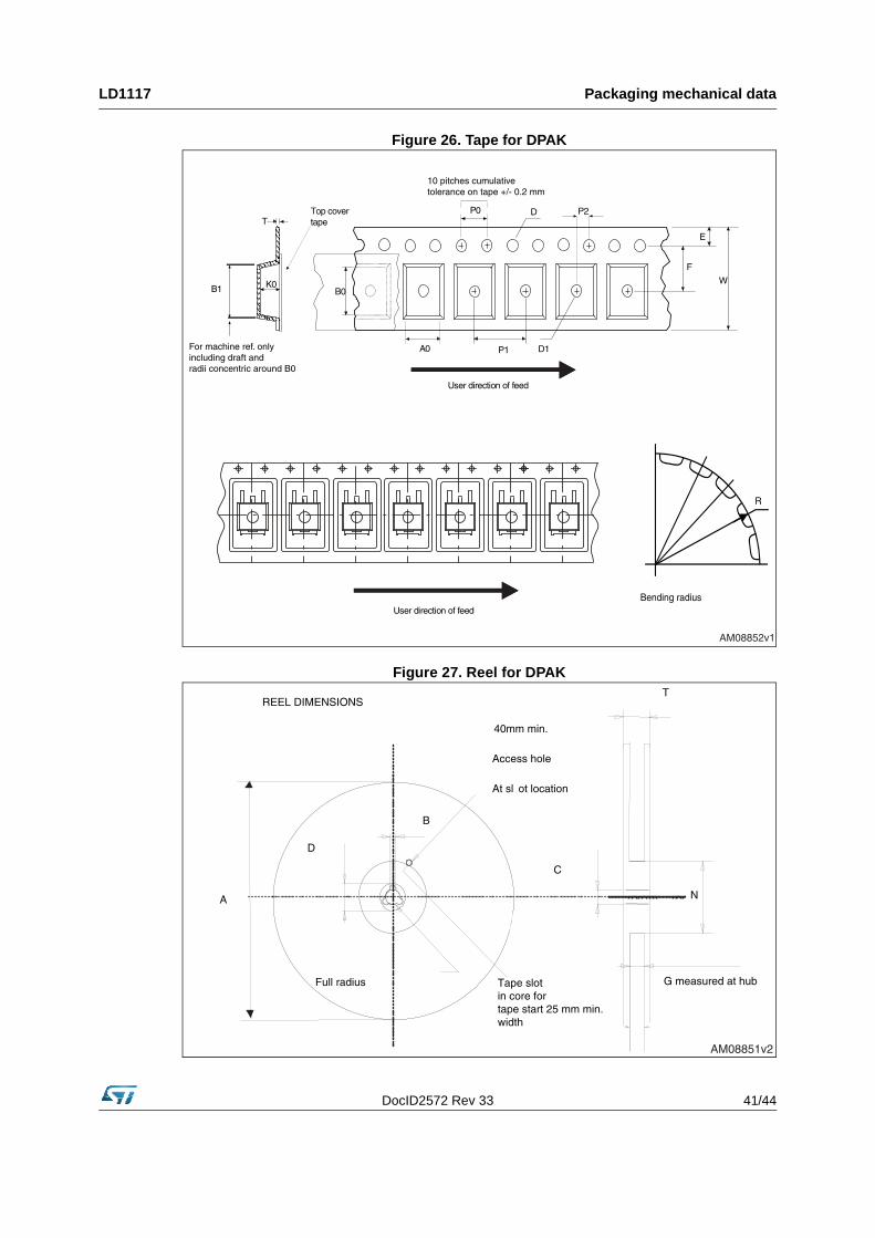
Figure 26. Tape for DPAK
Figure 27. Reel for DPAK
P1A0 D1
P0
F
W
E
D
B0K0
T
User direction of feed
P2
10 pitches cumulativetolerance on tape +/- 0.2 mm
User direction of feed
R
Bending radius
B1
For machine ref. onlyincluding draft andradii concentric around B0
AM08852v1
Top covertape
A
D
B
Full radius G measured at hub
C
N
REEL DIMENSIONS
40mm min.
Access hole
At sl ot location
T
Tape slot in core fortape start 25 mm min.width
AM08851v2
Order codes LD1117
42/44 DocID2572 Rev 33
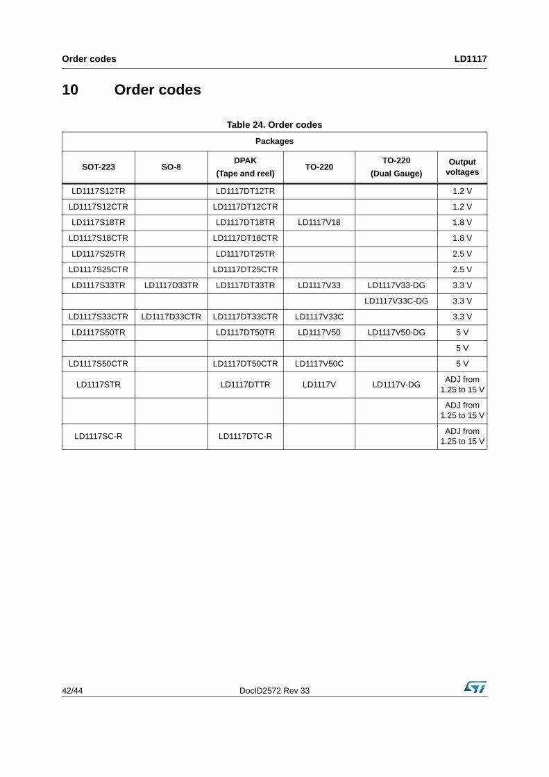
10 Order codes
Table 24. Order codes
Packages
SOT-223 SO-8DPAK
(Tape and reel)TO-220
TO-220
(Dual Gauge)Output
voltages
LD1117S12TR LD1117DT12TR 1.2 V
LD1117S12CTR LD1117DT12CTR 1.2 V
LD1117S18TR LD1117DT18TR LD1117V18 1.8 V
LD1117S18CTR LD1117DT18CTR 1.8 V
LD1117S25TR LD1117DT25TR 2.5 V
LD1117S25CTR LD1117DT25CTR 2.5 V
LD1117S33TR LD1117D33TR LD1117DT33TR LD1117V33 LD1117V33-DG 3.3 V
LD1117V33C-DG 3.3 V
LD1117S33CTR LD1117D33CTR LD1117DT33CTR LD1117V33C 3.3 V
LD1117S50TR LD1117DT50TR LD1117V50 LD1117V50-DG 5 V
5 V
LD1117S50CTR LD1117DT50CTR LD1117V50C 5 V
LD1117STR LD1117DTTR LD1117V LD1117V-DGADJ from
1.25 to 15 V
ADJ from 1.25 to 15 V
LD1117SC-R LD1117DTC-RADJ from
1.25 to 15 V
DocID2572 Rev 33 43/44
LD1117 Revision history
11 Revision history
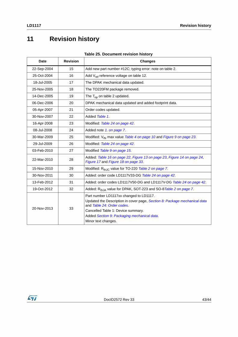
Table 25. Document revision history
Date Revision Changes
22-Sep-2004 15 Add new part number #12C; typing error: note on table 2.
25-Oct-2004 16 Add Vref reference voltage on table 12.
18-Jul-2005 17 The DPAK mechanical data updated.
25-Nov-2005 18 The TO220FM package removed.
14-Dec-2005 19 The Top on table 2 updated.
06-Dec-2006 20 DPAK mechanical data updated and added footprint data.
05-Apr-2007 21 Order codes updated.
30-Nov-2007 22 Added Table 1.
16-Apr-2008 23 Modified: Table 24 on page 42.
08-Jul-2008 24 Added note 1. on page 7.
30-Mar-2009 25 Modified: VIN max value Table 4 on page 10 and Figure 9 on page 23.
29-Jul-2009 26 Modified: Table 24 on page 42.
03-Feb-2010 27 Modified Table 9 on page 15.
22-Mar-2010 28Added: Table 16 on page 22, Figure 13 on page 23, Figure 14 on page 24, Figure 17 and Figure 18 on page 33.
15-Nov-2010 29 Modified: RthJC value for TO-220 Table 2 on page 7.
30-Nov-2011 30 Added: order code LD1117V33-DG Table 24 on page 42.
13-Feb-2012 31 Added: order codes LD1117V50-DG and LD1117V-DG Table 24 on page 42.
19-Oct-2012 32 Added: RthJA value for DPAK, SOT-223 and SO-8Table 2 on page 7.
20-Nov-2013 33
Part number LD1117xx changed to LD1117.Updated the Description in cover page, Section 8: Package mechanical data and Table 24: Order codes.Cancelled Table 1: Device summary.
Added Section 9: Packaging mechanical data.Minor text changes.
LD1117
44/44 DocID2572 Rev 33
Please Read Carefully:
Information in this document is provided solely in connection with ST products. STMicroelectronics NV and its subsidiaries (“ST”) reserve theright to make changes, corrections, modifications or improvements, to this document, and the products and services described herein at anytime, without notice.
All ST products are sold pursuant to ST’s terms and conditions of sale.
Purchasers are solely responsible for the choice, selection and use of the ST products and services described herein, and ST assumes noliability whatsoever relating to the choice, selection or use of the ST products and services described herein.
No license, express or implied, by estoppel or otherwise, to any intellectual property rights is granted under this document. If any part of thisdocument refers to any third party products or services it shall not be deemed a license grant by ST for the use of such third party productsor services, or any intellectual property contained therein or considered as a warranty covering the use in any manner whatsoever of suchthird party products or services or any intellectual property contained therein.
UNLESS OTHERWISE SET FORTH IN ST’S TERMS AND CONDITIONS OF SALE ST DISCLAIMS ANY EXPRESS OR IMPLIEDWARRANTY WITH RESPECT TO THE USE AND/OR SALE OF ST PRODUCTS INCLUDING WITHOUT LIMITATION IMPLIEDWARRANTIES OF MERCHANTABILITY, FITNESS FOR A PARTICULAR PURPOSE (AND THEIR EQUIVALENTS UNDER THE LAWSOF ANY JURISDICTION), OR INFRINGEMENT OF ANY PATENT, COPYRIGHT OR OTHER INTELLECTUAL PROPERTY RIGHT.
ST PRODUCTS ARE NOT DESIGNED OR AUTHORIZED FOR USE IN: (A) SAFETY CRITICAL APPLICATIONS SUCH AS LIFESUPPORTING, ACTIVE IMPLANTED DEVICES OR SYSTEMS WITH PRODUCT FUNCTIONAL SAFETY REQUIREMENTS; (B)AERONAUTIC APPLICATIONS; (C) AUTOMOTIVE APPLICATIONS OR ENVIRONMENTS, AND/OR (D) AEROSPACE APPLICATIONSOR ENVIRONMENTS. WHERE ST PRODUCTS ARE NOT DESIGNED FOR SUCH USE, THE PURCHASER SHALL USE PRODUCTS ATPURCHASER’S SOLE RISK, EVEN IF ST HAS BEEN INFORMED IN WRITING OF SUCH USAGE, UNLESS A PRODUCT ISEXPRESSLY DESIGNATED BY ST AS BEING INTENDED FOR “AUTOMOTIVE, AUTOMOTIVE SAFETY OR MEDICAL” INDUSTRYDOMAINS ACCORDING TO ST PRODUCT DESIGN SPECIFICATIONS. PRODUCTS FORMALLY ESCC, QML OR JAN QUALIFIED AREDEEMED SUITABLE FOR USE IN AEROSPACE BY THE CORRESPONDING GOVERNMENTAL AGENCY.
Resale of ST products with provisions different from the statements and/or technical features set forth in this document shall immediately voidany warranty granted by ST for the ST product or service described herein and shall not create or extend in any manner whatsoever, anyliability of ST.
ST and the ST logo are trademarks or registered trademarks of ST in various countries.Information in this document supersedes and replaces all information previously supplied.
The ST logo is a registered trademark of STMicroelectronics. All other names are the property of their respective owners.
© 2013 STMicroelectronics - All rights reserved
STMicroelectronics group of companies
Australia - Belgium - Brazil - Canada - China - Czech Republic - Finland - France - Germany - Hong Kong - India - Israel - Italy - Japan - Malaysia - Malta - Morocco - Philippines - Singapore - Spain - Sweden - Switzerland - United Kingdom - United States of America
www.st.com