Embed Size (px)
Citation preview

ADuCM3029 EZ-KIT ® Manual
Revision 1.0, February 2016
Part Number82-000637-01
Analog Devices, Inc.One Technology WayNorwood, MA 02062-9106

Copyright Information
© 2016 Analog Devices, Inc., ALL RIGHTS RESERVED. This document may not be reproduced in any formwithout prior, express written consent from Analog Devices, Inc.
Printed in the USA.
Disclaimer
Analog Devices, Inc. reserves the right to change this product without prior notice. Information furnished by Ana-log Devices is believed to be accurate and reliable. However, no responsibility is assumed by Analog Devices for itsuse; nor for any infringement of patents or other rights of third parties which may result from its use. No license isgranted by implication or otherwise under the patent rights of Analog Devices, Inc.
Trademark and Service Mark Notice
The Analog Devices logo, Blackfin, Blackfin+, SHARC, SHARC+, CrossCore, VisualDSP++, EZ-KIT, EZ-Extend-er, and EngineerZone are registered trademarks of Analog Devices, Inc.
All other brand and product names are trademarks or service marks of their respective owners.
Regulatory Compliance
The ADuCM3029 EZ-KIT is designed to be used solely in a laboratory environment. The board is not intended foruse as a consumer-end product or as a portion of a consumer-end product. The board is an open system design,which does not include a shielded enclosure and, therefore, may cause interference to other electrical devices in closeproximity. This board should not be used in or near any medical equipment or RF devices.
The ADuCM3029 EZ-KIT is in the process of being certified to comply with the essential requirements of the Euro-pean EMC directive 2004/108/EC and, therefore, carries the “CE” mark.
ADuCM3029 EZ-KIT ® Manual i

The ADuCM3029 EZ-KIT contains ESD (electrostatic discharge) sensitive devices. Electrostatic charges readily accu-mulate on the human body and equipment and can discharge without detection. Permanent damage may occur ondevices subjected to high-energy discharges. Proper ESD precautions are recommended to avoid performance degra-dation or loss of functionality. Store unused boards in the protective shiping package.
ADuCM3029 EZ-KIT ® Manual ii
Contents
Preface
Purpose of This Manual................................................................................................................................. 1–1
Intended Audience......................................................................................................................................... 1–1
Manual Contents ........................................................................................................................................... 1–2
Technical Support .......................................................................................................................................... 1–2
Supported Processors ..................................................................................................................................... 1–3
Supported Tools............................................................................................................................................. 1–3
Product Information...................................................................................................................................... 1–3
Analog Devices Website.............................................................................................................................. 1–3
EngineerZone ............................................................................................................................................. 1–4
Notation Conventions ................................................................................................................................... 1–4
Using the Board
Product Overview .......................................................................................................................................... 2–1
Package Contents........................................................................................................................................... 2–2
Default Configuration ................................................................................................................................... 2–3
IAR Embedded WorkBench Setup ................................................................................................................. 2–3
Debug Interface ............................................................................................................................................. 2–5
Power-On-Self Test........................................................................................................................................ 2–5
Power Measurements ..................................................................................................................................... 2–5
Example Programs ......................................................................................................................................... 2–5
Reference Design Information ....................................................................................................................... 2–5
32M-bit Serial Flash Memory with Dual and Quad SPI (W25Q32).............................................................. 2–6
ADuCM3029 EZ-KIT ® Manual iii

16-Bit Digital I2C Temperature Sensor (ADT7420) ...................................................................................... 2–6
Micropower 3-Sensor Combination Including Acceleration and Temperature (ADXL363) ........................... 2–7
USB to UART (FT232R)............................................................................................................................... 2–7
ADF7xxx Wireless Transceiver Daughterboard Interface................................................................................ 2–8
Arduino Interface........................................................................................................................................... 2–8
Expansion Interface 3 .................................................................................................................................... 2–8
Hardware Reference
System Architecture ....................................................................................................................................... 3–1
Switches......................................................................................................................................................... 3–2
Boot Mode Select ( SW1 )............................................................................................................................ 3–2
Reset Pushbutton ( SW2 )............................................................................................................................ 3–3
Wake Pushbutton ( SW3 ) ........................................................................................................................... 3–3
GPIO Pushbuttons ( SW4-5 )..................................................................................................................... 3–3
Jumpers ......................................................................................................................................................... 3–3
Main Power Select ( JP1 ) .......................................................................................................................... 3–4
IO Power Select ( JP2 ) .............................................................................................................................. 3–5
ADXL363 Power Enable ( JP3 )................................................................................................................. 3–5
W25Q32 Power Enable ( JP4 ) .................................................................................................................. 3–5
ADT7420 Power Enable ( JP5 )................................................................................................................. 3–5
Current Measurement ( JP6 )..................................................................................................................... 3–5
Remote Boot Select ( JP8 )......................................................................................................................... 3–5
Remote Reset ( JP9 ).................................................................................................................................. 3–6
WAKE Select ( JP10 ) ................................................................................................................................ 3–6
ADC VREF Select ( JP11 ) ........................................................................................................................ 3–6
Battery Select ( JP12 )................................................................................................................................ 3–6
LEDs ............................................................................................................................................................. 3–6
Reset ( LED1 )............................................................................................................................................. 3–7
iv ADuCM3029 EZ-KIT ® Manual

Power ( LED2 ) ........................................................................................................................................... 3–7
GPIO ( LED3-5 ) ....................................................................................................................................... 3–7
Connectors .................................................................................................................................................... 3–8
Expansion Interface 3 (P1A) ....................................................................................................................... 3–9
ADF7xxx Wireless Transceiver Daughterboard Interface (P1-3) ................................................................ 3–9
Debug (P4-5)............................................................................................................................................. 3–9
USB (P6) .................................................................................................................................................... 3–9
Power (P8)................................................................................................................................................ 3–10
Battery (J1 and J5) .................................................................................................................................. 3–10
PV Cell (J2) ............................................................................................................................................. 3–10
Clock (J3-4) ............................................................................................................................................ 3–10
Arduino Interface (J6-9) ......................................................................................................................... 3–11
ADuCM3029 EZ-KIT ® Manual v

1 Preface
Thank you for purchasing the Analog Devices, Inc. ADuCM3029 EZ-KIT ® evaluation system.
The ADuCM3029 processor is based on the ARM® Cortex®-M3 processor core, a collection of digital peripherals,embedded SRAM and flash memory. It also contains an analog subsystem which provides clocking, reset and powermanagement capability in addition to an ADC subsystem. The ADuCM3029 Microcontroller is designed specifical-ly for Motor Control and Industrial applications. The EZ-KIT ships with all of the necessary components requiredto start the evaluation immediately.
The EZ-KIT contains an array of three connectors that support the ADF7xxx Wireless Transceiver series of daugh-terboard products. Refer to ADF7xxx Wireless Transceiver Daughterboard Interface for more information.
The EZ-KIT contains an expansion interface 3 (EI3) and Arduino interface. These interfaces provide for connectingwith daughter boards to expand on the functionality of the EZ-KIT. Refer to Expansion Interface 3 and ArduinoInterface for more information
The evaluation board is designed to be used in conjunction with the IAR Embedded Workbench®and Segger®
development environment for advanced application code development and debug such as:
• Create, compile, assemble, and link application programs written in C++, C, and assembly
• Load, run, step, halt, and set breakpoints in application programs
• Read and write data and program memory
• Read and write core and peripheral registers
Purpose of This ManualThis manual provides instructions for installing the product hardware (board). The text describes operation andconfiguration of the board components and provides guidelines for running code on the board.
Intended AudienceThe primary audience for this manual is a programmer who is familiar with an ARM Cortex-M3-based processorcore. The ADuCM3029 family of mixed-signal control processors is based on the ARM Cortex-M3 core.
ADuCM3029 EZ-KIT ® Manual 1–1

For additional information about the Analog Devices processor, see the Hardware Reference Manual. The documentdescribes the core and memory architecture of the ADuCM3029 processor, but does not provide detailed program-ming information for the ARM core.
The applicable documentation for programming the ARM Cortex-M3 processor core includes:
• Cortex-M3 Devices Generic User Guide
• Cortex-M3 Technical Reference Manual
For more information about programming the ARM core, visit the ARM Information Center:
http://infocenter.arm.com/help/.
Manual ContentsThe manual consists of:
• Using the board
Provides basic board information.
• Hardware Reference
Provides information about the hardware aspects of the board.
• Bill of Matrials
A companion file in PDF format that lists all of the components used on the board is available in the installa-tion directory for the Board Support Package (BSP) and on http://www.analog.com/ADuCM3029EZKIT .
• Schematic
A companion file in PDF format documenting all of the circuits used on the board is available in the installa-tion directory for the Board Support Package (BSP) and on http://www.analog.com/ADuCM3029EZKIT .
Technical SupportYou can reach Analog Devices processors and DSP technical support in the following way
• Post your questions in the processors and DSP support community at EngineerZone®:
http://ez.analog.com/community/dsp
• Submit your questions to technical support directly at:
http://www.analog.com/support
• E-mail your questions about processors, DSPs, and tools development software from CrossCore Embedded Stu-dio or VisualDSP++®:
Manual Contents
1–2 ADuCM3029 EZ-KIT ® Manual
If using CrossCore Embeded Studio or VisualDSP++ choose Help > Email Support. This creates an e-mail [email protected] and automatically attaches your CrossCore Embedded Studio or Visu-alDSP++ version information and license.dat file.
• E-mail your questions about processors and processor applications to:
• Contact your Analog Devices sales office or authorized distributor. Locate one at:
http://www.analog.com/adi-sales
• Send questions by mail to:
Analog Devices, Inc.
One Technology Way
P.O. Box 9106
Norwood, MA 02062-9106
USA
Supported ProcessorsThis evaluation system supports the Analog Devices ADuCM3029 processor.
Supported ToolsInformation about code development tools for the ADuCM3029 EZ-KIT and ADuCM3029 family of processors isavailable at:
http://www.analog.com/ADuCM3029EZKIT .
Product InformationProduct information can be obtained from the Analog Devices Website
Analog Devices Website
The Analog Devices website, http://www.analog.com, provides information about a broad range of products - ana-log integrated circuits, amplifiers, converters, and digital signal processors.
To access a complete technical library for each processor family, go to http://www.analog.com/processors/techni-cal_library. The manuals selection opens a list of current manuals related to the product as well as a link to theprevious revisions of the manuals. When locating your manual title, note a possible errata check mark next to thetitle that leads to the current correction report against the manual.
Supported Processors
ADuCM3029 EZ-KIT ® Manual 1–3

Also note, MyAnalog.com is a free feature of the Analog Devices website that allows customization of a web page todisplay only the latest information about products you are interested in. You can choose to receive weekly e-mailnotifications containing updates to the web pages that meet your interests, including documentation errata againstall manuals. MyAnalog.com provides access to books, application notes, data sheets, code examples, and more.
Visit MyAnalog.com to sign up. If you are a registered user, just log on. Your user name is your e-mail address.
EngineerZone
EngineerZone is a technical support forum from Analog Devices, Inc. It allows you direct access to ADI technicalsupport engineers. You can search FAQs and technical information to get quick answers to your embedded process-ing and DSP design questions.
Use EngineerZone to connect with other DSP developers who face similar design challenges. You can also use thisopen forum to share knowledge and collaborate with the ADI support team and your peers. Visit http://ez.analog.com to sign up.
Notation ConventionsText conventions used in this manual are identified and described as follows. Additional conventions, which applyonly to specific chapters, may appear throughout this document.
Example Description
File > Close Titles in bold style indicate the location of an item within the CrossCore Embed-ded Studio IDE’s menu system (for example, the Close command appears on theFile menu).
{this | that} Alternative required items in syntax descriptions appear within curly brackets andseparated by vertical bars; read the example as this or that. One or the other isrequired.
[this | that] Optional items in syntax descriptions appear within brackets and separated byvertical bars; read the example as an optional this or that.
[this, …] Optional item lists in syntax descriptions appear within brackets delimited bycommas and terminated with an ellipsis; read the example as an optional comma-separated list of this.
.SECTION Commands, directives, keywords, and feature names are in text with lettergothic font.
filename Non-keyword placeholders appear in text with letter gothic font and italicstyle format.
NOTE:
NOTE: For correct operation, ..
A note provides supplementary information on a related topic. In the online ver-sion of this book, the word NOTE: appears instead of this symbol.
Product Information
1–4 ADuCM3029 EZ-KIT ® Manual

Example Description
CAUTION:
CAUTION: Incorrect device operation may result if ..
CAUTION: Device damage may result if ..
A caution identifies conditions or inappropriate usage of the product that couldlead to undesirable results or product damage. In the online version of this book,the word CAUTION: appears instead of this symbol.
ATTENTION:
ATTENTION: Injury to device users may result if ..
A warning identifies conditions or inappropriate usage of the product that couldlead to conditions that are potentially hazardous for devices users. In the onlineversion of this book, the word ATTENTION: appears instead of this symbol.
Notation Conventions
ADuCM3029 EZ-KIT ® Manual 1–5

2 Using the Board
This chapter provides information on the major components and peripherals on the board along with instrustionsfor installing and setting up the emualtion software.
Product OverviewThe board features:
• Analog Devices ADuCM3029 processor
• 64-pin QFN package
• 26 MHz oscillator
• SPI Flash (SPI2) chip
• 32Mb
• Windbond W25Q32
• Accelerometer (SPI2)
• Analog Devices ADXL363
• Temp sensor
• Analog Devices ADT7420
• Universal Asynchronous Receiver/Transmitter (UART0)
• FTDI FT232R USB to UART IC
• USB mini-B
• Debug (SWD/SWO) interface
• J-Link Lite ARM debugger
• SWD/SWO 20-pin 0.1” header for use with IAR emulators
• SWD/SWO 10-pin 0.05” header
• LEDs
ADuCM3029 EZ-KIT ® Manual 2–1

• Five LEDs: one power (green), one board reset (red), and three general-purpose (amber)
• Pushbuttons
• Five pushbuttons: one reset, one wake, boot and two IRQ/Flag
• Expansion Interface 3 (EI3) connector
• CLKOUT
• SPORT0
• SPI1
• UART0
• TWI0
• Timers
• GPIOs
• RESET• GND/3.3V/5V output
• Arduino interface
• ADF7xxx Wireless Transceiver Daughterboard interface
• External power supply
• CE compliant
• 5V @ 3.6 Amps
• Power measurement
• Jumpers for measuring processor and board current draw
Package ContentsYour ADuCM3029 EZ-KIT package contains the following items.
• ADuCM3029 EZ-KIT board
• Universal 5V DC power supply
• USB 2.0 cable
• J-Link Lite emulator
Contact the vendor where you purchased your EZ-KIT or contact Analog Devices, Inc. if any item is missing.
Package Contents
2–2 ADuCM3029 EZ-KIT ® Manual

Default ConfigurationThe ADuCM3029 EZ-KIT board is designed to run as a standalone unit.
The Default Hardware Setup figure shows the default settings for jumpers and switches and the location of thejumpers, switches, connectors, and LEDs. Confirm that your board is in the default configuration before using theboard.
P4
P1A
J3
J4
P7
J8
P6P5
J7
J5
J2
P1
P3J1
P2
P8
P9
J9J6
JP1JP10
JP5
JP9
JP8
JP11
JP4
JP12JP2
JP3
JP13
JP6 LED3
LED4
LED5
LED2 LED1SW3
SW2
SW4
SW1
SW5
Figure 2-1: Default Hardware Setup
IAR Embedded WorkBench SetupFor information about the IAR Embedded Workbench®and Segger® product and software download, go to:
http://www.iar.com/en/Products/IAR-Embedded-Workbench.
Default Configuration
ADuCM3029 EZ-KIT ® Manual 2–3

The ADuCM3029 EZ-KIT software, based on the IAR Embedded WorkBench, can be found at:
http://www.analog.com/ADuCM3029EZKIT
Follow these instructions to ensure correct operation of the product software and hardware.
1. Connect the EZ-KIT board to a personal computer (PC) running IAR Embedded WorkBench, using a J-Link/J-Trace emulator:
a. Plug one side of the USB cable into the USB connector of the emulator. Plug the other side into a USBport of the PC running IAR Embedded WorkBench.
b. Attach the emulator to the header connector, P4 or P5, on the EZ-KIT board.
2. Attach the provided cord and appropriate plug to the 5V power adapter:
a. Plug the jack-end of the power adapter into the power connector P8 on the EZ-KIT board.
b. Plug the other side of the power adapter into a power outlet. The power LED ( LED2 ) is lit green whenpower is applied to the board.
It is assumed that the IAR Embedded WorkBench software is installed and running on your PC.
1. Navigate to the IAR Embedded WorkBench environment via the Start menu.
2. Choose File > Open > Workspace to open a workspace for the project to download and debug.
3. Choose Project > Options.
The General Options, Target page appears.
4. In Processor variant, ensure Device is Analog Devices ADuCM302x
5. Choose Debugger in the Category pane.
The Debugger, Setup options page appears.
a. In Driver, choose J-Link/J-Trace as the emulator to be used to debug the target board.
b. Click the Download tab. The Debugger, Download options page appears.
c. Ensure Use flash loader(s) is enabled. Note that other download settings are optional.
6. Choose Debugger > J-Link/J-Trace in the Category pane.
The emulator Setup options page appears.
a. On the Setup page,
• In Reset, select Connect during reset from the drop-down list.
• In JTAG/SWD speed, select Auto.
• (Optional) In Clock setup, change the default values.
b. On the Connection page,
IAR Embedded WorkBench Setup
2–4 ADuCM3029 EZ-KIT ® Manual

• In Communication, select USB and Device 0.
• In Interface, select SWD.
7. Click OK to save the emulator settings.
8. Choose Project > Debug and Download to download the project and start debugging.
Debug InterfaceThe EZ-KIT provides a SWD/SWO connection via P4 or P5.
Power-On-Self TestThe Power-On-Self-Test Program (POST) tests all EZ-KIT peripherals and validates functionality as well as connec-tivity to the processor. Once assembled, each EZ-KIT is fully tested for an extended period of time with POST. AllEZ-KITs boards are shipped with POST preloaded into flash memory. The POST is executed by resetting the boardand pressing the proper push button(s). The POST also can be used as a reference for a custom software design orhardware troubleshooting.
Note that the source code for the POST program is included in the Board Support Package (BSP) along with thereadme.txt file that describes how the board is configured to run POST.
Power MeasurementsLocations are provided for measuring the current draw from various power planes. Jumpers are available on theMAIN_3V and PROC_3V voltage domains. For current draw, the jumper is removed and a precision ammeter insert-ed in series. The board allows for measuring the current draw of just the processor by removing the jumper on pins1 and 3 and inserting an ammeter. Current draw can be measured in all operating modes of the processor. Refer toCurrent Measurement ( JP6 ).
Example ProgramsExample programs are provided with the ADuCM3029 EZ-KIT Board Support Package (BSP) to demonstrate vari-ous capabilities of the product. The programs can be found in the ADuCM3029_EZ-KIT\examples installationfolder. Refer to a readme file provided with each example for more information.
Reference Design InformationA reference design info package is available for download on the Analog Devices Web site. The package providesinformation on the schematic design, layout, fabrication, and assembly of the board.
The information can be found at:
http://www.analog.com/ADuCM3029EZKIT .
Debug Interface
ADuCM3029 EZ-KIT ® Manual 2–5

32M-bit Serial Flash Memory with Dual and Quad SPI(W25Q32)The W25Q32BV (32 Mb) Serial Flash memory provides a storage solution for systems with limited space, pins andpower. The 25Q series offers flexibility and performance well beyond ordinary Serial Flash devices. They are idealfor code shadowing to RAM, executing code directly from Dual/Quad SPI (XIP) and storing voice, text and data.The device operates on a single 2.7V to 3.6V power supply with current consumption as low as 4 mA active and 1uA for power-down.
The W25Q32BV array is organized into 16,384 programmable pages of 256 bytes each. Up to 256 bytes can beprogrammed at a time. Pages can be erased in a group of 16 (4 KB sector erase), groups of 128 (32 KB block erase),groups of 256 (64 KB block erase) or the entire chip (chip erase). The W25Q32BV has 1024 erasable sectors and 64erase blocks respectively. The small 4 KB sectors allow for greater flexibility in applications that require data andparameter storage.
The W25Q32BV supports the standard Serial Peripheral Interface (SPI), and a high performance Dual/Quad ouputas well as Dual/Quad I/O SPI: Serial Clock, Chip Select, Serial Data I/O0 (DI), I/O1 (DO), I/O2 (WP), and I/O3(/HOLD). SPI clock frequencies of up to 104 MHz are supported, providing equivalent clock rates of 208 MHz(104 MHz x 2) for Dual I/O and 320 MHz (80 MHz x 4) for Quad I/O when using Fast Read Dual/Quad I/Oinstructions. These transfer rates can outperform standard Asynchronous 8 and 16-bit Parallel Flash memories. TheContinous Read Mode allows for efficient memory access with as few as 8-clocks of instruction-overhead to read a24-bit address, allowing true XIP (execute in place) operation.
16-Bit Digital I2C Temperature Sensor (ADT7420)The ADT7420 is a high-accuracy digital-temperature sensor offering breakthrough performance over a wide indus-trial range, housed in a 4 mm × 4 mm LFCSP package. It contains an internal band gap reference, a temperaturesensor, and a 16-bit ADC to monitor and digitize the temperature to 0.0078°C resolution. The ADC resolution, bydefault, is set to 13 bits (0.0625°C). The ADC resolution is a user-programmable mode that can be changedthrough the serial interface.
The ADT7420 is guaranteed to operate over supply voltages from 2.7V to 5.5V. Operating at 3.3V, the averagesupply current is typically 210 μA. The ADT7420 has a shutdown mode that powers down the device and offers ashutdown current of typically 2.0 μA at 3.3V. The ADT7420 is rated for operation over the -40°C to +150°C tem-perature range.
Pins A0 and A1 are available for address selection, giving the ADT7420 four possible I2C addresses. The CT pin isan open-drain output that becomes active when the temperature exceeds a programmable critical temperature limit.The INT pin is also an open-drain output that becomes active when the tempera-ture exceeds a programmable limit.The INT pin and CT pin can operate in comparator and interrupt event modes.
32M-bit Serial Flash Memory with Dual and Quad SPI (W25Q32)
2–6 ADuCM3029 EZ-KIT ® Manual

Micropower 3-Sensor Combination Including Accelerationand Temperature (ADXL363)The ADXL363 is an ultralow power, three-sensor combination consisting of a 3-axis MEMS accelerometer, a tem-perature sensor, and an on-board ADC input for synchronous conversion of an external signal. The entire systemconsumes less than 2 μA at a 100 Hz output data rate and 270 nA when in motion triggered wake-up mode.
The ADXL363 communicates via a serial port interface (SPI) and always provides 12-bit output resolution for allthree sensors.
The ADXL363 accelerometer provides selectable measurement ranges of ±2 g, ±4 g, and ±8 g, with a resolution of 1mg/LSB on the ±2 g range. Unlike accelerometers that use power duty cycling to achieve low power consumption,the ADXL363 does not alias input signals by undersampling; it samples the full bandwidth of the sensor at all datarates.
The ADXL363 temperature sensor operates with a scale factor of 0.065°C (typical). Acceleration and temperaturedata can be stored in a 512-sample multimode FIFO buffer, allowing up to 13 sec of data to be stored.
In addition to the accelerometer and temperature sensor, the ADXL363 also provides access to an internal ADC forsynchronous conversion of an additional analog input.
The ADXL363 operates on a wide 1.6V to 3.5V supply range and can interface, if necessary, to a host operating ona separate, lower supply voltage.
USB to UART (FT232R)The FT232R is a USB-to-serial-UART interface with the following advanced features:
• Single chip USB to asynchronous serial data transfer interface
• Entire USB protocol handled on the chip. No USB specific firmware programming required
• Fully-integrated 1024 bit EEPROM storing device descriptors and CBUS I/O configuration
• Fully-integrated USB termination resistors
• Fully-integrated clock generation with no external crystal required, plus optional clock output selection ena-bling a glue-less interface to external MCU or FPGA
• Data transfer rates from 300 baud to 3 Mbaud (RS422, RS485, RS232) at TTL levels
• 128 byte receive buffer and 256 byte transmit buffer utilising buffer smoothing technology to allow for high-data throughput
• FTDI’s royalty-free Virtual Com Port (VCP) and Direct (D2XX) drivers eliminate the requirement for USBdriver development in most cases.
• Transmit and receive LED drive signals
• UART interface support for 7 or 8 data bits, 1 or 2 stop bits and odd / even / mark / space / no parity
Micropower 3-Sensor Combination Including Acceleration and Temperature (ADXL363)
ADuCM3029 EZ-KIT ® Manual 2–7

• FIFO receives and transmits buffers for high-data throughput
• Device supplied pre-programmed with unique USB serial number
• Supports bus powered, self-powered and high-power bus powered USB configurations
• Integrated +3.3V level converter for USB I/O
• Integrated level converter on UART and CBUS for interfacing to between +1.8V and +5V logic
• True 5V/3.3V/2.8V/1.8V CMOS drive output and TTL input
• Configurable I/O pin output drive strength
• Integrated power-on-reset circuit
• Fully-integrated AVCC supply filtering - no external filtering required.
• UART signal inversion option
• +3.3V (using external oscillator) to +5.25V (internal oscillator) single supply operation
• Low-operating and USB suspend current
• Low USB bandwidth consumption
• UHCI/OHCI/EHCI host controller compatible
• USB 2.0 full speed compatible
ADF7xxx Wireless Transceiver Daughterboard InterfaceThe ADF7xxx Wireless Transceiver daughterboard interface supports the ADF7023, ADF7024, ADF7242,ADF7030 and ADF7030-1 wireless transceivers. These are low-power, high-performance, integrated radio transceiv-ers supporting a wide range of modulation schemes and channel widths in the sub-GHz and 2.4 GHz frequencyranges.
"For more information about Analog Devices Transceiver offerings please visit : http://www.analog.com/en/prod-ucts/rf-microwave/integrated-transceivers-transmitters-receivers/low-power-rf-transceivers.html
Arduino InterfaceThe Arduino interface supports connecting with 3V shield boards, extending the evaluation sysem's capabilities.The connectors provide power, ground, reset, ADC, TWI, UART and GPIO signals.
Expansion Interface 3The Expansion Interface 3 (EI3) interface supports connecting with other EI3 daughterboards designed by AnalogDevices, extending the evaluation system's capabilities. The connectors provide power, ground, reset, ADC, TWI,UART, SPORT and GPIO signals.
ADF7xxx Wireless Transceiver Daughterboard Interface
2–8 ADuCM3029 EZ-KIT ® Manual

3 Hardware Reference
This chapter describes the hardware design of the ADuCM3029 EZ-KIT .
System ArchitectureThe board's configuration is shown in the Block Diagram figure.
ADSP-ADuCM3029LEDs (3)
Deb
ug
Port
SPI2
26 MHz crystal
PBs (2)
CLK
IN
GPI
O
UART0
SWD10 pin 0.05"
EI3 (1A)
SWD 20 pin 0.1"
32 Mbit SPI Flash
ADF7xxx daughterboard
RTC
ADP7102Wall 3.3V
FTDIFT232RQ
USB
32.768 kHz crystal
J-Link
ADC
SPI
SPORT
ADXl363
I2C0
ADT7420
USB
Arduino Interface
SPORT
TMR
GPIOI2C
UART0
SPI
Figure 3-1: Block Diagram
This EZ-KIT is designed to demonstrate the ADuCM3029 processor’s capabilities. The board has a 26 MHz inputclock and runs at 26 MHz internally.
ADuCM3029 EZ-KIT ® Manual 3–1

User I/O to the processor is provided in the form of two user pushbuttons and three LEDs.
SwitchesThis section describes operation of the switches. The switch locations are shown in the Switch Locations figure.
SW3
SW2
SW4
SW1
SW5
Figure 3-2: Switch Locations
Boot Mode Select ( SW1 )
The pushbutton switch determines the boot mode of the processor. The Boot Mode Select Switch table shows theavailable boot mode settings. By default, the processor boots from the internal flash memory.
Switches
3–2 ADuCM3029 EZ-KIT ® Manual
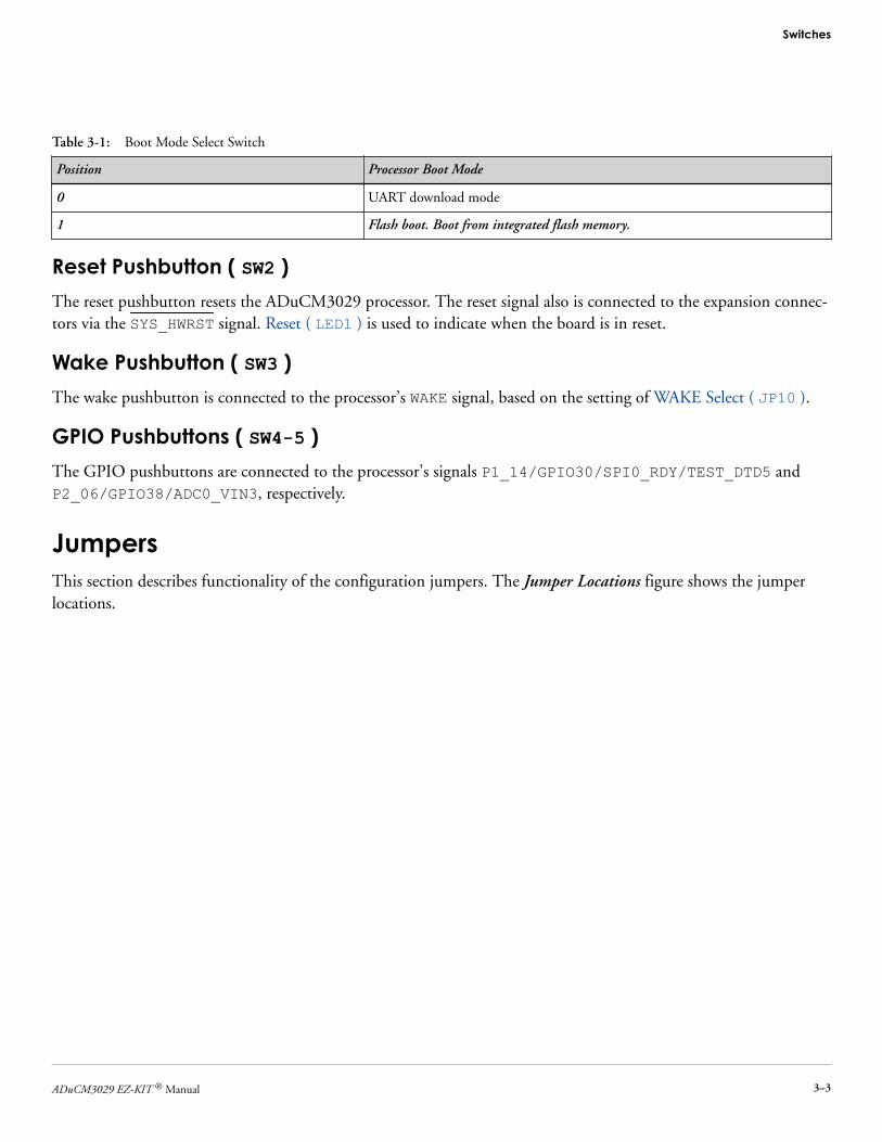
Table 3-1: Boot Mode Select Switch
Position Processor Boot Mode
0 UART download mode
1 Flash boot. Boot from integrated flash memory.
Reset Pushbutton ( SW2 )
The reset pushbutton resets the ADuCM3029 processor. The reset signal also is connected to the expansion connec-tors via the SYS_HWRST signal. Reset ( LED1 ) is used to indicate when the board is in reset.
Wake Pushbutton ( SW3 )
The wake pushbutton is connected to the processor’s WAKE signal, based on the setting of WAKE Select ( JP10 ).
GPIO Pushbuttons ( SW4-5 )
The GPIO pushbuttons are connected to the processor’s signals P1_14/GPIO30/SPI0_RDY/TEST_DTD5 andP2_06/GPIO38/ADC0_VIN3, respectively.
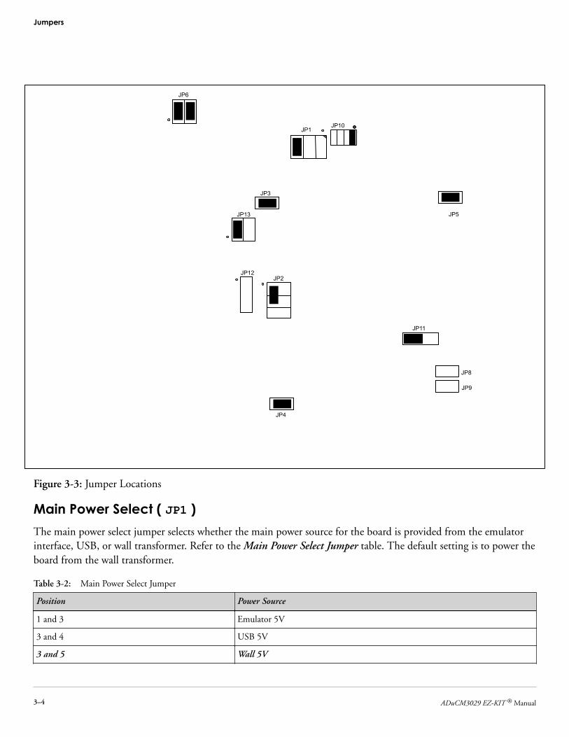
JumpersThis section describes functionality of the configuration jumpers. The Jumper Locations figure shows the jumperlocations.
Switches
ADuCM3029 EZ-KIT ® Manual 3–3
JP1JP10
JP5
JP9
JP8
JP11
JP4
JP12JP2
JP3
JP13
JP6
Figure 3-3: Jumper Locations
Main Power Select ( JP1 )
The main power select jumper selects whether the main power source for the board is provided from the emulatorinterface, USB, or wall transformer. Refer to the Main Power Select Jumper table. The default setting is to power theboard from the wall transformer.
Table 3-2: Main Power Select Jumper
Position Power Source
1 and 3 Emulator 5V
3 and 4 USB 5V
3 and 5 Wall 5V
Jumpers
3–4 ADuCM3029 EZ-KIT ® Manual

IO Power Select ( JP2 )
The IO power select jumper selects whether the IO power source for the board is provided from the on-board 3Vregualtor, coin battery, or PV cell battery. Refer to the IO Power Select Jumper table. The default setting is to powerthe IO from the on-board regualtor.
Table 3-3: IO Power Select Jumper
Position Power Source
1 and 3 on-board regualtor
3 and 4 coin battery
3 and 5 PV cell
ADXL363 Power Enable ( JP3 )
The ADXL363 power enable jumper allows the part to be connected or disconnected from the IO power rail. Whenthe jumper is installed, the device is connected to power. When the jumper is removed, power is disconnected fromthe device. The device can be removed from the power rail to yield more accurate current measurements of the IOrail when the device is not needed. The default is for the jumper to be installed.
W25Q32 Power Enable ( JP4 )
The W25Q32 power enable jumper allows the part to be connected or disconnected from the IO power rail. Whenthe jumper is installed, the device is connected to power. When the jumper is removed, power is disconnected fromthe device. The device can be removed from the power rail to yeld more accurate current measurements of the IOrail when the device is not needed. The default is for the jumper to be installed.
ADT7420 Power Enable ( JP5 )
The ADT7420 power enable jumper allows the part to be connected or disconnected from the IO power rail. Whenthe jumper is installed, the device is connected to power. When the jumper is removed, power is disconnected fromthe device. The device can be removed from the power rail to yeld more accurate current measurements of the IOrail when the device is not needed. The default is for the jumper to be installed.
Current Measurement ( JP6 )
The current measurement jumper is used to measure the current draw of the processor and 3V IO power rail. Thedefault is for both jumpers to be installed. To measure the current draw of the processor, remove the jumper frompins 1 and 3 and insert an ammeter in series. In order to measure the current draw on the 3V IO rail remove thejumper from pins 2 and 4 and insert an ammeter in series.
Remote Boot Select ( JP8 )
The remote boot select jumper allows the SYS_BMODE0 to be controlled by the FT232 when the jumper is installed.The default is for the jumper not to be installed.
Jumpers
ADuCM3029 EZ-KIT ® Manual 3–5

Remote Reset ( JP9 )
The remote reset jumper allows the SYS_HWRST to be controlled by the FT232 when the jumper is installed. Thedefault is for the jumper not to be installed.
WAKE Select ( JP10 )
This jumper is used to determine which WAKE signal from the processor is connected to the Wake Pushbutton( SW3 ); see the Wake Jumpers table. The default setting is on pins 1 and 2.
Table 3-4: WAKE Jumpers
Setting Signal
1 and 2 SYS_WAKE0
3 and 4 SYS_WAKE1
5 and 6 SYS_WAKE2
7 and 8 SYS_WAKE3
ADC VREF Select ( JP11 )
The ADC VREF select jumper it used to connect the ADC voltage reference of the processor to either the ADR441or the ADR127 device. When the jumper is placed on pins 1 and 2, the reference is conencted to the ADR441,which is a ultralow noise, LDO XFET voltage reference with current sink and source. When the jumper is placed onpins 2 and 3, the reference is connected to the ADR127, which is a precisoin micropower LDO voltage reference.By default the jumper is connected to pins 2 and 3.
Battery Select ( JP12 )
The battery select jumper is used to choose between powering the board with a coin battery or a AA battery. Whenthe jumper is installed on pins 1 and 2, the coin cell battery is selected. When the jumper is installed on pins 2 and3, the AA battery is selected. By default, the jumper only connected to pin 1 - neither battery is connected.
LEDsThis section describes the on-board LEDs. The LED Locations figure shows the LED locations.
Jumpers
3–6 ADuCM3029 EZ-KIT ® Manual

LED3
LED4
LED5
LED2 LED1
Figure 3-4: LED Locations
Reset ( LED1 )
When ON (red), it indicates that the board is in reset. A master reset is asserted by pressing SW2 , which activatesthe LED. For more information, see Reset Pushbutton ( SW2 ).
Power ( LED2 )
When ON (green), it indicates that power is being supplied to the board properly.
GPIO ( LED3-5 )
Three LEDs are connected to the general-purpose I/O pins of the processor (see the GPIO LEDs table). The LEDsare active high and are ON (amber) by writing a 1 to the correct processor signal.
LEDs
ADuCM3029 EZ-KIT ® Manual 3–7

Table 3-5: GPIO LEDs
LED Reference Designator Processor Programmable Flag Pin
LED3 P0_13
LED4 P1_12
LED5 P1_13
ConnectorsThis section describes connector functionality and provides information about mating connectors. The connectorlocations are shown in the Connector Locations figure.
P4
P1A
J3
J4
P7
J8
P6P5
J7
J5
J2
P1
P3J1
P2
P8
P9
J9J6
Figure 3-5: Connector Locations
NOTE: Connectors on the back of the board are noted with dotted lines.
Connectors
3–8 ADuCM3029 EZ-KIT ® Manual

Expansion Interface 3 (P1A)
One board-to-board connector provides signals from the SPI, TWI, UART, SPORT, and GPIO interfaces of theprocessor. This connector is located on the bottom side of the board. The connector expands the board's capabilitiesby providing an interface to EI3 daughterboards.
Part Description Manufacturer Part Number
120-pin 0.6mm Hirose FX8-120P-SV1(91)
Mating Connector
120-pin 0.6mm Hirose FX8-120S-SV(21)
ADF7xxx Wireless Transceiver Daughterboard Interface (P1-3)
ADF7xxx wireless transceiver daughterboard interface connectors are listed in the following tables.
Table 3-6: P1 and P2 Connectors
Part Description Manufacturer Part Number
10-pin 0.05" terminal strip Samtec TFM-105-02-S-D-A
Mating Connector
10-pin 0.05" socket strip Samtec SFM-105-02-L-D-A
Table 3-7: P3 Connectors
Part Description Manufacturer Part Number
20-pin 0.05" terminal strip Samtec TFM-110-02-S-D-A
Mating Connector
20-pin 0.05" socket strip Samtec SFM-110-02-L-D-A
Debug (P4-5)
The debug connectors provides a connection point for the emualtor to interface with the processor. There are twodebug connectors on the board. The P4 connector is a 0.1” 20 pin connector. The P5 connector is a 0.05" 10 pinconnector. For more information, see Debug Interface.
USB (P6)
The USB connector provides an interface between the EZ-KIT and a host PC via the USB to UART (FT232R).
Part Description Manufacturer Part Number
USB mini-B Hirose UX60SC-MB-5S8
Connectors
ADuCM3029 EZ-KIT ® Manual 3–9

Power (P8)
The power connector provides power to the board when the jumper of Main Power Select ( JP1 ) is placed on pins3 and 5.
Part Description Manufacturer Part Number
0.65 mm power jack CUI 045-0883R
Mating Connector
[email protected] power supplier GLOBETEK GS-1750(R)
Battery (J1 and J5)
A battery can be used to power the board by setting the IO Power Select ( JP2 ).
Table 3-8: J1 Connector
Part Description Manufacturer Part Number
Coincell Holder MPD BS-3
Battery
3V 20mm Coin Panasonic CR2032
Table 3-9: J5 Connector
Part Description Manufacturer Part Number
AA Holder Keystone Electronics 2460
Battery
3.6V 2.6Ah AA Dantona Industries LS14500
PV Cell (J2)
This conenctor is used for interfacing with engery harvesting evaluation boards from Analog Devices.
Part Description Manufacturer Part Number
8-pin 0.1" right angle Harwin M20-7880446
Clock (J3-4)
The clock connectors allow for a connection point to the SYS_CLKIN and SYS_CLKOUT signals on the processor.
Part Description Manufacturer Part Number
SMC 75 ohms Amphenol 152119-75
Mating Cable
SMC cable
Connectors
3–10 ADuCM3029 EZ-KIT ® Manual

Arduino Interface (J6-9)
The connectors for the Arduino interface are listed in the following tables.
Table 3-10: J6 Connector
Part Description Manufacturer Part Number
8-pin 0.1" socket strip Samtec SSW-108-01-TM-S
Mating Connector
8-pin .1" terminal strip Samtec TSW-108-07-T-S
Table 3-11: J7-9 Connectors
Part Description Manufacturer Part Number
10-pin 0.1" socket strip Samtec SSW-110-01-TM-S
Mating Connector
10-pin .1" terminal strip Samtec TSW-110-07-T-S
Connectors
ADuCM3029 EZ-KIT ® Manual 3–11

ADuCM3029 EZ-KIT ® Manual