Embed Size (px)
Citation preview
REV. A
a
Information furnished by Analog Devices is believed to be accurate andreliable. However, no responsibility is assumed by Analog Devices for itsuse, nor for any infringements of patents or other rights of third parties thatmay result from its use. No license is granted by implication or otherwiseunder any patent or patent rights of Analog Devices.
One Technology Way, P.O. Box 9106, Norwood, MA 02062-9106, U.S.A.
Tel: 781/329-4700 www.analog.com
Fax: 781/326-8703 © Analog Devices, Inc., 2002
ADV7300A/ADV7301A
Multiformat SD, Progressive Scan/HDTVVideo Encoder with Six NSV™ 12-Bit DACs
NSV (Noise Shaped Video) is a trademark of Analog Devices, Inc.*ADV7300A Only
FEATURES
High Definition Input Formats
YCrCb Compliant to SMPTE293M (525 p),
ITU-R.BT1358 (625 p), SMPTE274M (1080 i),
SMPTE296M (720 p), and Any Other High Definition
Standard Using Async Timing Mode
RGB in 3 10-Bit 4:4:4 Format
BTA T-1004 EDTV2 525 p Parallel
High Definition Output Formats (525 p/625 p/720 p/1080 i)
YPrPb Progressive Scan (EIA-770.1, EIA-770.2)
YPrPb HDTV (EIA 770.3)
RGB + H/V (HDTV 5-Wire Format)
CGMS-A (720 p/1080 i)
Macrovision Rev 1.0 (525 p/625 p)*
CGMS-A (525 p)
Standard Definition Input Formats
CCIR-656 4:2:2 8-/10-Bit Parallel Input
CCIR-601 4:2:2 16-/20-Bit Parallel Input
Standard Definition Output Formats
Composite NTSC M, N;
PAL M, N, B, D, G, H, I, PAL-60
SMPTE170M NTSC Compatible Composite Video
ITU-R.BT470 PAL Compatible Composite Video
S-Video (Y/C)
EuroScart RGB
Component YUV (Betacam, MII, SMPTE/EBU N10)
Macrovision Rev 7.1*
CGMS/WSS
Closed Captioning
GENERAL FEATURES
Simultaneous SD and HD Inputs and Outputs
Oversampling (108 MHz/148.5 MHz)
On-Board Voltage Reference
6 NSV Precision Video 12-Bit DACs
2-Wire Serial MPU Interface
Dual I/O Supply 2.5 V/3.3 V Operation
Analog and Digital Supply 2.5 V
On-Board PLL
64-LQFP Package
Lead-Free Product
APPLICATIONS
High End DVD Players
SD/Program Scan/HDTV Display Devices
SD/Program Scan/HDTV Set-Top Boxes
SD/HDTV Studio Equipment
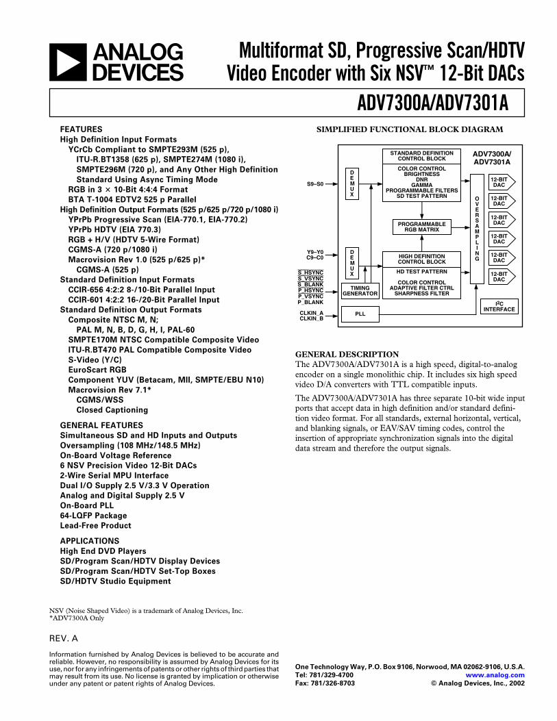
SIMPLIFIED FUNCTIONAL BLOCK DIAGRAM
S9–S0
Y9–Y0C9–C0
S_HSYNCS_VSYNCS_BLANKP_HSYNCP_VSYNCP_BLANK
CLKIN_ACLKIN_B
DEMUX
TIMINGGENERATOR
PLL
OVERSAMPLING
I2CINTERFACE
DEMUX
STANDARD DEFINITIONCONTROL BLOCK
COLOR CONTROLBRIGHTNESS
DNRGAMMA
PROGRAMMABLE FILTERSSD TEST PATTERN
HIGH DEFINITIONCONTROL BLOCK
HD TEST PATTERN
COLOR CONTROLADAPTIVE FILTER CTRL
SHARPNESS FILTER
PROGRAMMABLERGB MATRIX
12-BITDAC
12-BITDAC
12-BITDAC
12-BITDAC
12-BITDAC
12-BITDAC
ADV7300A/ADV7301A
GENERAL DESCRIPTIONThe ADV7300A/ADV7301A is a high speed, digital-to-analogencoder on a single monolithic chip. It includes six high speedvideo D/A converters with TTL compatible inputs.
The ADV7300A/ADV7301A has three separate 10-bit wide inputports that accept data in high definition and/or standard defini-tion video format. For all standards, external horizontal, vertical,and blanking signals, or EAV/SAV timing codes, control theinsertion of appropriate synchronization signals into the digitaldata stream and therefore the output signals.
REV. A–2–
ADV7300A/ADV7301A
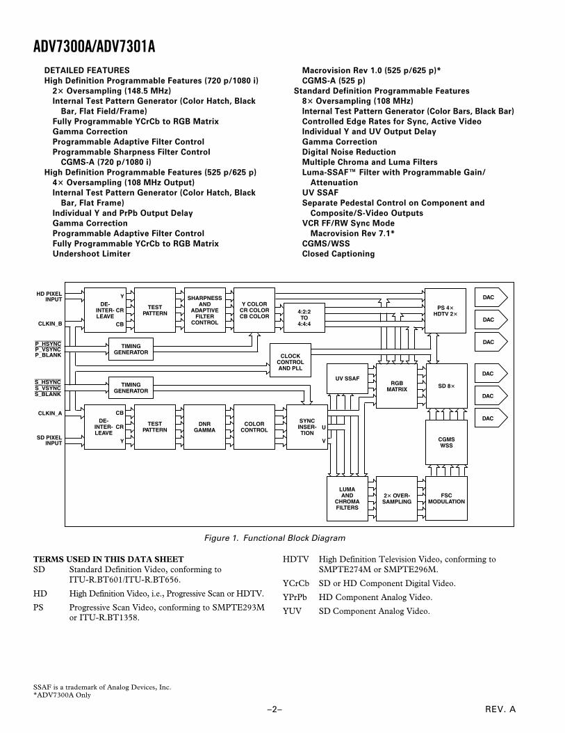
FSCMODULATION
S_HSYNCS_VSYNCS_BLANK
CLKIN_A
P_HSYNCP_VSYNCP_BLANK
CLKIN_B
HD PIXELINPUT
SD PIXELINPUT
DE-INTER-LEAVE
Y
CB
CR TESTPATTERN
SHARPNESSAND
ADAPTIVEFILTER
CONTROL
Y COLORCR COLORCB COLOR
4:2:2TO
4:4:4
TIMINGGENERATOR
TIMINGGENERATOR
DE-INTER-LEAVE
Y
CB
CR TESTPATTERN
DNRGAMMA
COLORCONTROL
SYNCINSER-TION
CLOCKCONTROLAND PLL
2 OVER-SAMPLING
UV SSAF
V
U
PS 4HDTV 2
RGBMATRIX
SD 8
LUMAAND
CHROMAFILTERS
CGMSWSS
DAC
DAC
DAC
DAC
DAC
DAC
Figure 1. Functional Block Diagram
DETAILED FEATURES
High Definition Programmable Features (720 p/1080 i)
2 Oversampling (148.5 MHz)
Internal Test Pattern Generator (Color Hatch, Black
Bar, Flat Field/Frame)
Fully Programmable YCrCb to RGB Matrix
Gamma Correction
Programmable Adaptive Filter Control
Programmable Sharpness Filter Control
CGMS-A (720 p/1080 i)
High Definition Programmable Features (525 p/625 p)
4 Oversampling (108 MHz Output)
Internal Test Pattern Generator (Color Hatch, Black
Bar, Flat Frame)
Individual Y and PrPb Output Delay
Gamma Correction
Programmable Adaptive Filter Control
Fully Programmable YCrCb to RGB Matrix
Undershoot Limiter
TERMS USED IN THIS DATA SHEETSD Standard Definition Video, conforming to
ITU-R.BT601/ITU-R.BT656.
HD High Definition Video, i.e., Progressive Scan or HDTV.
PS Progressive Scan Video, conforming to SMPTE293Mor ITU-R.BT1358.
Macrovision Rev 1.0 (525 p/625 p)*
CGMS-A (525 p)
Standard Definition Programmable Features
8 Oversampling (108 MHz)
Internal Test Pattern Generator (Color Bars, Black Bar)
Controlled Edge Rates for Sync, Active Video
Individual Y and UV Output Delay
Gamma Correction
Digital Noise Reduction
Multiple Chroma and Luma Filters
Luma-SSAF™ Filter with Programmable Gain/
Attenuation
UV SSAF
Separate Pedestal Control on Component and
Composite/S-Video Outputs
VCR FF/RW Sync Mode
Macrovision Rev 7.1*
CGMS/WSS
Closed Captioning
SSAF is a trademark of Analog Devices, Inc.*ADV7300A Only
HDTV High Definition Television Video, conforming toSMPTE274M or SMPTE296M.
YCrCb SD or HD Component Digital Video.
YPrPb HD Component Analog Video.
YUV SD Component Analog Video.
REV. A –3–
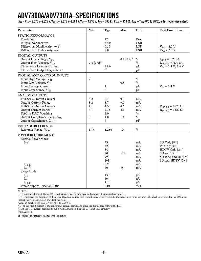
ADV7300A/ADV7301A–SPECIFICATIONS
Parameter Min Typ Max Unit Test Conditions
STATIC PERFORMANCE1
Resolution 12 BitsIntegral Nonlinearity ±2.0 LSBDifferential Nonlinearity, +ve2 0.25 LSB VAA = 2.5 VDifferential Nonlinearity, –ve2 2.0 LSB VAA = 2.5 V
DIGITAL OUTPUTSOutput Low Voltage, VOL 0.4 [0.4]3 V ISINK = 3.2 mAOutput High Voltage, VOH 2.4 [2.0]3 V ISOURCE = 400 µAThree-State Leakage Current ±1.0 µA VIN = 0.4 V, 2.4 VThree-State Output Capacitance 2 pF
DIGITAL AND CONTROL INPUTSInput High Voltage, VIH 2 VInput Low Voltage, VIL 0.8 VInput Leakage Current 1 µA VIN = 2.4 VInput Capacitance, CIN 2 pF
ANALOG OUTPUTSFull-Scale Output Current 8.2 8.7 9.2 mAOutput Current Range 8.2 8.7 9.2 mAFull-Scale Output Current 4.1 4.35 4.6 mA RSET1, 2 = 1520 ΩOutput Current Range 4.1 4.35 4.6 mA RSET1, 2 = 1520 ΩDAC to DAC Matching 2.0 %Output Compliance Range, VOC 0 1.0 1.4 VOutput Capacitance, COUT 7 pF
VOLTAGE REFERENCEReference Range, VREF 1.15 1.235 1.3 V
POWER REQUIREMENTSNormal Power Mode
IDD4 93 mA SD Only [8]
52 mA PS Only [4]84 mA HDTV Only [2]90 110 mA SD and PS99 mA SD [8] and HDTV108 mA SD and HDTV [2]
IDD_IO 0.2 mAIAA
5,6 70 75 mASleep Mode
IDD 130 µAIAA 10 µAIDD_IO 110 µA
Power Supply Rejection Ratio 0.01 %/%
NOTES1Oversampling disabled. Static DAC performance will be improved with increased oversampling ratios.2DNL measures the deviation of the actual DAC o/p voltage step from the ideal. For +ve DNL, the actual step value lies above the ideal step value; for –ve DNL, theactual step values lie below the ideal step value.
3Value in brackets for VDD_IO = 2.375 V to 2.750 V.4IDD or the circuit current is the continuous current required to drive the digital core without the I PLL.5IAA is the total current required to supply all DACs including the VREF and PLL circuitry.6All DACs on.
Specifications subject to change without notice.
(VAA = VDD = 2.375 V–2.625 V, VDD_IO = 2.375 V–3.600 V, VREF = 1.235 V, RSET = 760 , RLOAD = 150 , TMIN to TMAX (0C to 70C), unless otherwise noted.)
REV. A–4–
ADV7300A/ADV7301A
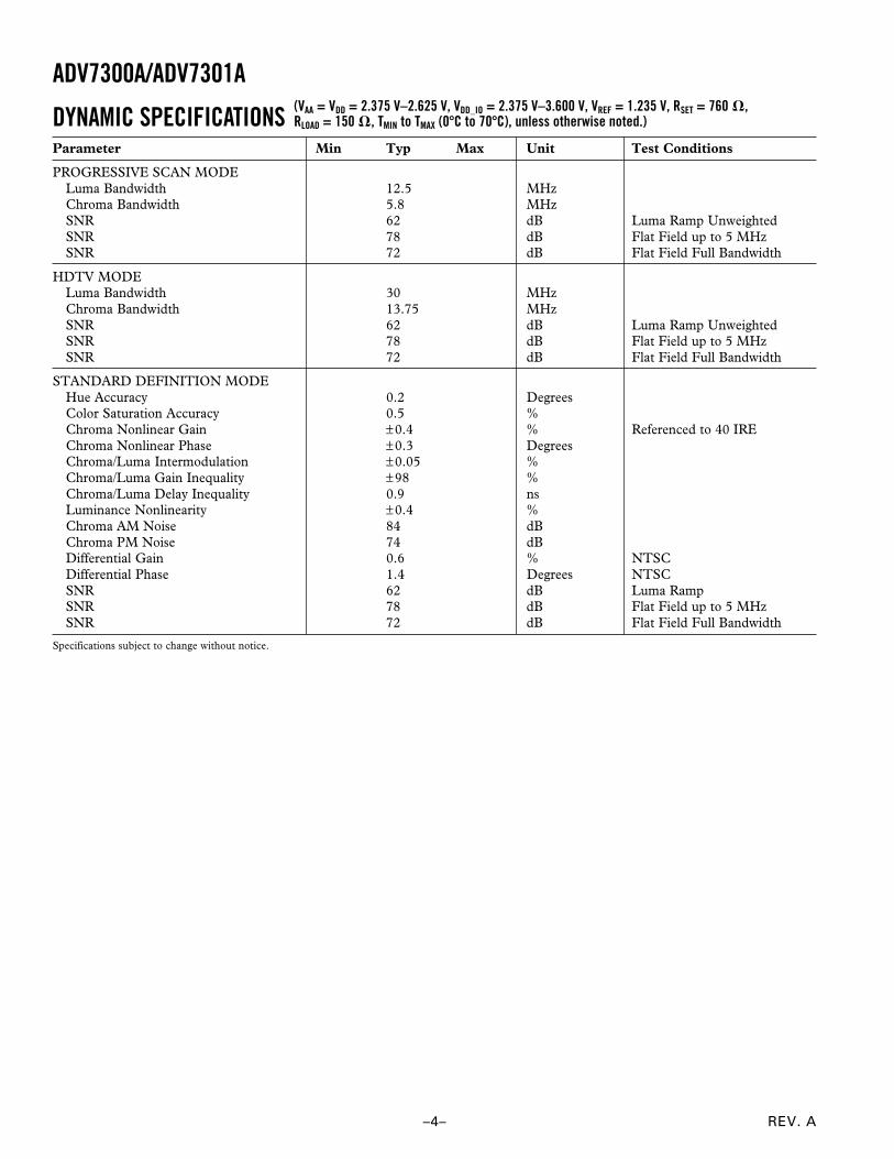
DYNAMIC SPECIFICATIONSParameter Min Typ Max Unit Test Conditions
PROGRESSIVE SCAN MODELuma Bandwidth 12.5 MHzChroma Bandwidth 5.8 MHzSNR 62 dB Luma Ramp UnweightedSNR 78 dB Flat Field up to 5 MHzSNR 72 dB Flat Field Full Bandwidth
HDTV MODELuma Bandwidth 30 MHzChroma Bandwidth 13.75 MHzSNR 62 dB Luma Ramp UnweightedSNR 78 dB Flat Field up to 5 MHzSNR 72 dB Flat Field Full Bandwidth
STANDARD DEFINITION MODEHue Accuracy 0.2 DegreesColor Saturation Accuracy 0.5 %Chroma Nonlinear Gain ±0.4 % Referenced to 40 IREChroma Nonlinear Phase ±0.3 DegreesChroma/Luma Intermodulation ±0.05 %Chroma/Luma Gain Inequality ±98 %Chroma/Luma Delay Inequality 0.9 nsLuminance Nonlinearity ±0.4 %Chroma AM Noise 84 dBChroma PM Noise 74 dBDifferential Gain 0.6 % NTSCDifferential Phase 1.4 Degrees NTSCSNR 62 dB Luma RampSNR 78 dB Flat Field up to 5 MHzSNR 72 dB Flat Field Full Bandwidth
Specifications subject to change without notice.
(VAA = VDD = 2.375 V–2.625 V, VDD_IO = 2.375 V–3.600 V, VREF = 1.235 V, RSET = 760 ,RLOAD = 150 , TMIN to TMAX (0C to 70C), unless otherwise noted.)
REV. A
ADV7300A/ADV7301A
–5–
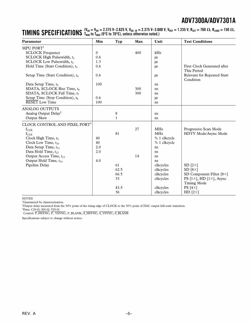
TIMING SPECIFICATIONSParameter Min Typ Max Unit Test Conditions
MPU PORT1
SCLOCK Frequency 0 400 kHzSCLOCK High Pulsewidth, t1 0.6 µsSCLOCK Low Pulsewidth, t2 1.3 µsHold Time (Start Condition), t3 0.6 µs First Clock Generated after
This PeriodSetup Time (Start Condition), t4 0.6 µs Relevant for Repeated Start
ConditionData Setup Time, t5 100 nsSDATA, SCLOCK Rise Time, t6 300 nsSDATA, SCLOCK Fall Time, t7 300 nsSetup Time (Stop Condition), t8 0.6 µsRESET Low Time 100 ns
ANALOG OUTPUTSAnalog Output Delay2 8 nsOutput Skew 1 ns
CLOCK CONTROL AND PIXEL PORT3
fCLK 27 MHz Progressive Scan ModefCLK 81 MHz HDTV Mode/Async ModeClock High Time, t9 40 % 1 clkcycleClock Low Time, t10 40 % 1 clkcycleData Setup Time, t11 2.0 nsData Hold Time, t12 2.0 nsOutput Access Time, t13 14 nsOutput Hold Time, t14 4.0 nsPipeline Delay 61 clkcycles SD [2]
62.5 clkcycles SD [8]66.5 clkcycles SD Component Filter [8]33 clkcycles PS [1], HD [1], Async
Timing Mode43.5 clkcycles PS [4]36 clkcycles HD [2]
NOTES1Guaranteed by characterization.2Output delay measured from the 50% point of the rising edge of CLOCK to the 50% point of DAC output full-scale transition.3Data: C[9:0]; S[9:0]; Y[9:0]Control: P_HSYNC; P_ VSYNC; P_BLANK; S_HSYNC; S_VSYNC; S_BLANK
Specifications subject to change without notice.
(VAA = VDD = 2.375 V–2.625 V, VDD_IO = 2.375 V–3.600 V, VREF = 1.235 V, RSET = 760 , RLOAD = 150 ,TMIN to TMAX (0C to 70C), unless otherwise noted.)
REV. A–6–
ADV7300A/ADV7301A
t9
t11
CLKIN_A
C9–C0
t10 t12
P_HSYNC,P_VSYNC,P_BLANK
Cb0 Cr0 Cb2 Cr2 Cb4 Cr4
CONTROLI/PS
Y0 Y1 Y2 Y3 Y4 Y5 Y9–Y0
t14
CONTROLO/PS
S_HSYNC,S_VSYNC
t13
t9 = CLOCK HIGH TIME, t10 = CLOCK LOW TIME, t11 = DATA SETUP TIME, t12 = DATA HOLD TIME
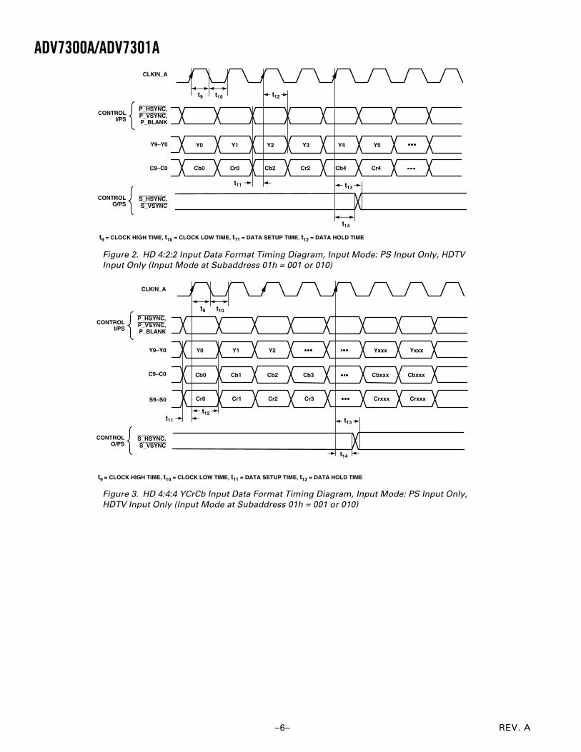
Figure 2. HD 4:2:2 Input Data Format Timing Diagram, Input Mode: PS Input Only, HDTVInput Only (Input Mode at Subaddress 01h = 001 or 010)
t9
t11
t10
t12
t13
t14
CLKIN_A
C9–C0
P_HSYNC,P_VSYNC,P_BLANK
CONTROLI/PS
Y9–Y0
CONTROLO/PS
S_HSYNC,S_VSYNC
t9 = CLOCK HIGH TIME, t10 = CLOCK LOW TIME, t11 = DATA SETUP TIME, t12 = DATA HOLD TIME
S9–S0
Y0 Y1 Y2 Yxxx Yxxx
Cb0 Cb1 Cb2 Cb3 Cbxxx Cbxxx
Cr0 Cr1 Cr2 Cr3 Crxxx Crxxx
Figure 3. HD 4:4:4 YCrCb Input Data Format Timing Diagram, Input Mode: PS Input Only,HDTV Input Only (Input Mode at Subaddress 01h = 001 or 010)
REV. A
ADV7300A/ADV7301A
–7–
t9
t11
t10
t12
t13
t14
CLKIN_A
C9–C0
P_HSYNC,P_VSYNC,P_BLANK
CONTROLI/PS
Y9–Y0
CONTROLO/PS
S_HSYNC,S_VSYNC
t9 = CLOCK HIGH TIME, t10 = CLOCK LOW TIME, t11 = DATA SETUP TIME, t12 = DATA HOLD TIME
S9–S0
G0 G1 G2 Gxxx Gxxx
B0 B1 B2 B3 Bxxx Bxxx
R0 R1 R2
G3
Rxxx Rxxx
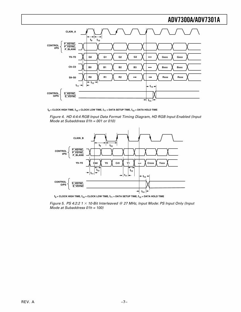
Figure 4. HD 4:4:4 RGB Input Data Format Timing Diagram, HD RGB Input Enabled (InputMode at Subaddress 01h = 001 or 010)
t9
t11
t10
t12
t11
t12
t13
t14
CLKIN_B
Y9–Y0
P_HSYNC,P_VSYNC,P_BLANK
CONTROLI/PS
CONTROLO/PS S_HSYNC,
S_VSYNC
t9 = CLOCK HIGH TIME, t10 = CLOCK LOW TIME, t11 = DATA SETUP TIME, t12 = DATA HOLD TIME
Cb0 Y0 Cr0 Y1 Crxxx Yxxx
Figure 5. PS 4:2:2 1 10-Bit Interleaved @ 27 MHz, Input Mode: PS Input Only (InputMode at Subaddress 01h = 100)
REV. A–8–
ADV7300A/ADV7301A
t9
t11
t10
t12
Cb0 Y0 Cr0 Y1 Crxxx Yxxx
t14
t13
CLKIN_A
Y9–Y0
P_HSYNC,P_VSYNC,P_BLANK
CONTROLI/PS
CONTROLO/PS
S_HSYNC,S_VSYNC
t9 = CLOCK HIGH TIME, t10 = CLOCK LOW TIME, t11 = DATA SETUP TIME, t12 = DATA HOLD TIME
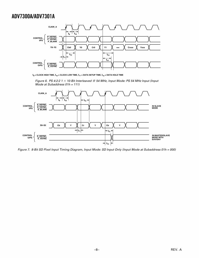
Figure 6. PS 4:2:2 1 10-Bit Interleaved @ 54 MHz, Input Mode: PS 54 MHz Input (InputMode at Subaddress 01h = 111)
t9
t11
t10 t12
Cb Y Cr Y Cb Y
t13
t14
CLKIN_A
S9–S2
S_HSYNC,S_VSYNC,S_BLANK
CONTROLI/PS
CONTROLO/PS
S_HSYNC,S_VSYNC
IN SLAVEMODE
IN MASTER/SLAVEMODE WITHEAV/SAV
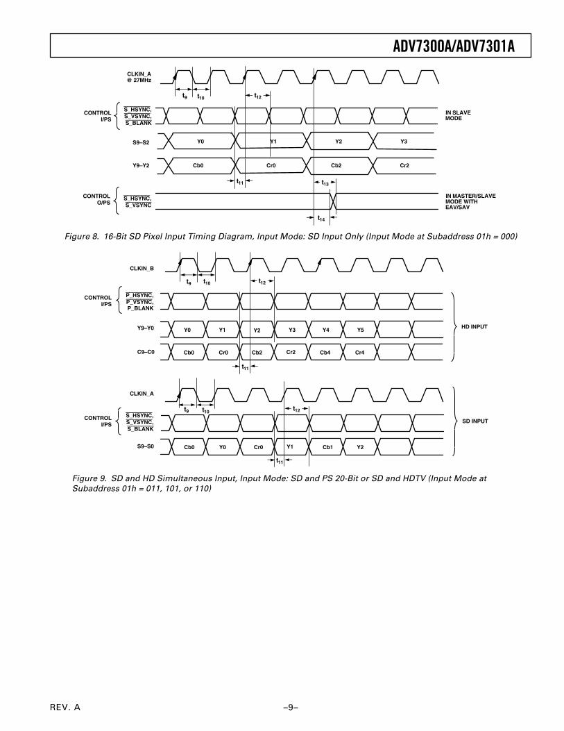
Figure 7. 8-Bit SD Pixel Input Timing Diagram, Input Mode: SD Input Only (Input Mode at Subaddress 01h = 000)
REV. A
ADV7300A/ADV7301A
–9–
t9
t11
CLKIN_A@ 27MHz
S9–S2
t10 t12
S_HSYNC,S_VSYNC,S_BLANK
t13
t14
CONTROLI/PS
CONTROLO/PS
S_HSYNC,S_VSYNC
Y9–Y2
IN SLAVEMODE
IN MASTER/SLAVEMODE WITHEAV/SAV
Y0 Y1 Y2 Y3
Cb0 Cr0 Cb2 Cr2
Figure 8. 16-Bit SD Pixel Input Timing Diagram, Input Mode: SD Input Only (Input Mode at Subaddress 01h = 000)
t9
t11
t10 t12
Cb0 Cr0 Cb2 Cr2 Cb4 Cr4
Y0 Y1 Y2 Y3 Y4 Y5
Cb0 Y0 Cr0 Y1 Cb1 Y2
t9 t10
t11
t12
HD INPUT
SD INPUT
S9–S0
S_HSYNC,S_VSYNC,S_BLANK
CONTROLI/PS
CLKIN_A
CLKIN_B
Y9–Y0
CONTROLI/PS
P_HSYNC,P_VSYNC,P_BLANK
C9–C0
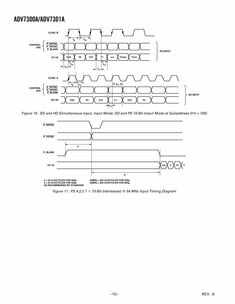
Figure 9. SD and HD Simultaneous Input, Input Mode: SD and PS 20-Bit or SD and HDTV (Input Mode atSubaddress 01h = 011, 101, or 110)
REV. A–10–
ADV7300A/ADV7301A
S9–S0 Cb0 Y0 Cr0 Y1 Cb1 Y2
S_HSYNC,S_VSYNC,S_BLANK
CONTROLI/PS
CLKIN_A
t9 t10
t11
t12
SD INPUT
t9
t11
CLKIN_B
Y9–Y0
t10
t12
t11
t12
CONTROLI/PS
P_HSYNC,P_VSYNC,P_BLANK
PS INPUT
Crxxx Yxxx Cb0 Y0 Cr0 Y1
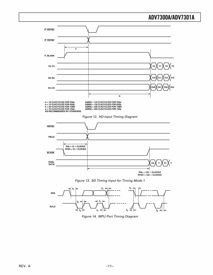
Figure 10. SD and HD Simultaneous Input, Input Mode: SD and PS 10-Bit (Input Mode at Subaddress 01h = 100)
P_HSYNC
P_VSYNC
P_BLANK
Y9–Y0 Cb Y Cr Y
b
a
a = 32 CLKCYCLES FOR 525pa = 24 CLKCYCLES FOR 625pAS RECOMMENDED BY STANDARD
b(MIN) = 244 CLKCYCLES FOR 525pb(MIN) = 264 CLKCYCLES FOR 625p
Figure 11. PS 4:2:2 1 10-Bit Interleaved @ 54 MHz Input Timing Diagram
REV. A
ADV7300A/ADV7301A
–11–
P_HSYNC
P_VSYNC
P_BLANK
Y9–Y0 Y0 Y1 Y2 Y3
Cr0 Cr1 Cr2 Cr3
Cb0 Cb1 Cb2 Cb3
b
a
a = 16 CLKCYCLES FOR 525pa = 12 CLKCYCLES FOR 626pa = 44 CLKCYCLES FOR 1080ia = 70 CLKCYCLES FOR 720pAS RECOMMENDED BY STANDARD
S9–S0
C9–C0
b(MIN) = 122 CLKCYCLES FOR 525pb(MIN) = 132 CLKCYCLES FOR 625pb(MIN) = 236 CLKCYCLES FOR 1080ib(MIN) = 300 CLKCYCLES FOR 720p
Figure 12. HD Input Timing Diagram
HSYNC
FIELD
BLANK
PIXELDATA
PAL = 12 CLOCK/2NTSC = 16 CLOCK/2
PAL = 132 CLOCK/2NTSC = 122 CLOCK/2
Cb Y Cr Y
Figure 13. SD Timing Input for Timing Mode 1
t3
t1 t6
t2 t7
t5 t3
t4 t8
SDA
SCLK
Figure 14. MPU Port Timing Diagram
REV. A–12–
ADV7300A/ADV7301A
CAUTIONESD (electrostatic discharge) sensitive device. Electrostatic charges as high as 4000 V readilyaccumulate on the human body and test equipment and can discharge without detection. Although theADV7300A/ADV7301A features proprietary ESD protection circuitry, permanent damage may occuron devices subjected to high energy electrostatic discharges. Therefore, proper ESD precautions arerecommended to avoid performance degradation or loss of functionality.
ABSOLUTE MAXIMUM RATINGS*
VAA to AGND . . . . . . . . . . . . . . . . . . . . . . . . +3.0 V to –0.3 VVDD to GND . . . . . . . . . . . . . . . . . . . . . . . . . +3.0 V to –0.3 VVDD_IO to IO_GND . . . . . . . . . . . . . –0.3 V to VDD_IO + 0.3 VAmbient Operating Temperature (TA) . . . . . . . 0°C to +70°CStorage Temperature (TS) . . . . . . . . . . . . . . –65°C to +150°CInfrared Reflow Soldering (20 sec) . . . . . . . . . . . . . . . . 260°C*Stresses above those listed under Absolute Maximum Ratings may causepermanent damage to the device. This is a stress rating only; functional opera-tion of the device at these or any other conditions above those listed in theoperational sections of this specification is not implied. Exposure to absolutemaximum rating conditions for extended periods may affect device reliability.
THERMAL CHARACTERISTICS
θJC = 11ºC/W
θJA = 47ºC/W
PIN CONFIGURATION
1
2
3
4
5
6
7
8
9
10
11
12
13
14
15
16
PIN 1IDENTIFIER
TOP VIEW(Not to Scale)
VDD_IO 48
47
46
45
44
43
42
41
40
39
38
37
36
35
34
33
49505152535455565758596061626364
32313029282726252423222120191817
Y0
Y1
Y2
Y3
Y4
Y5
Y6
Y7
VDD
DGND
Y8
Y9
C0
C1
C2
S_BLANKRSET1
VREF
COMP1
DAC A
DAC B
DAC C
VAA
AGND
DAC D
DAC E
DAC F
COMP2
RSET2
EXT_LF
RESET
C3
C4
I2C
AL
SB
SD
A
SC
LK
P_H
SY
NC
P_V
SY
NC
P_B
LA
NK C5
C6
C7
C8
C9
RT
C_S
CR
_TR
CL
KIN
_A
GN
D_I
O
CL
KN
_B
S9
S8
S7
S6
S5
DG
ND
VD
D
S4
S3
S2
S1
S0
S_H
SY
NC
S_V
SY
NC
ADV7300A/ADV7301A
ORDERING GUIDE
Model Package Description Package Option
ADV7300AKST Plastic Quad Flatpack ST-64BADV7301AKST Plastic Quad Flatpack ST-64B
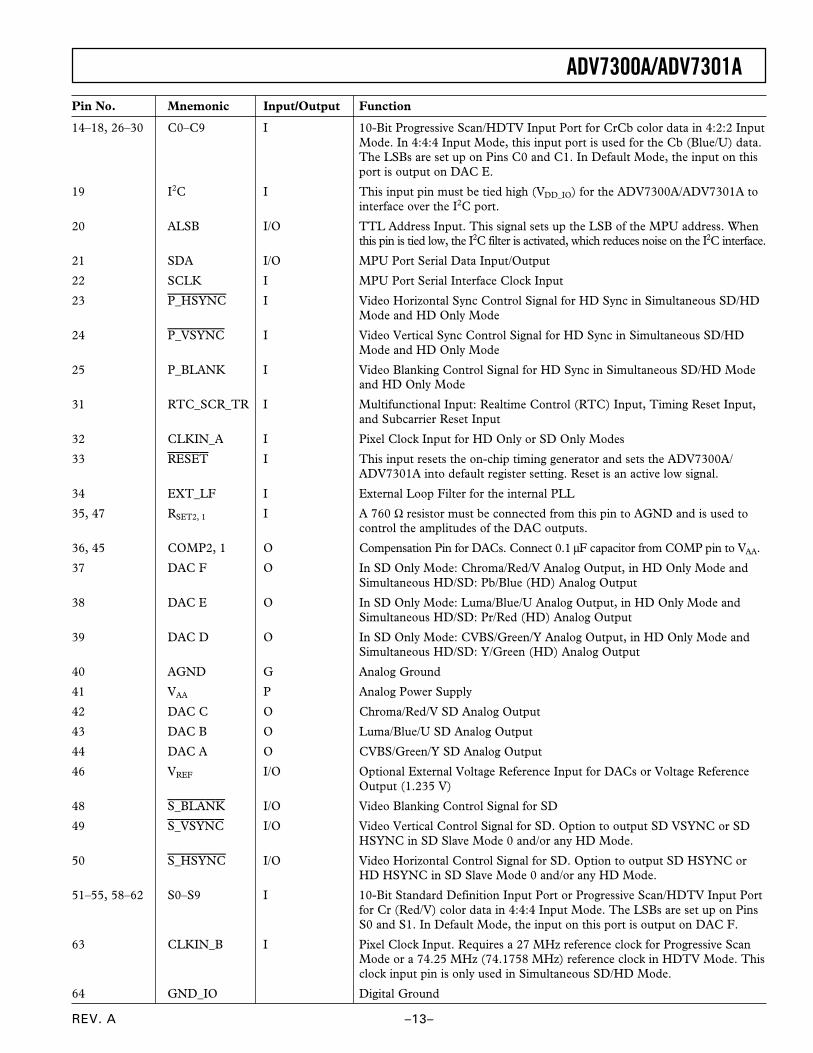
PIN FUNCTION DESCRIPTIONS
Pin No. Mnemonic Input/Output Function
1 VDD_IO P Power Supply for Digital Inputs and Outputs
2–9, 12, 13 Y0–Y9 I 10-Bit Progressive Scan/HDTV Input Port for Y Data. The LSBs are set up onPins Y0 and Y1. In Default Mode, the input on this port is output on DAC D.
10, 56 VDD P Digital Power Supply
11, 57 DGND G Digital Ground
The ADV7300A/ADV7301A is a lead-free environmentallyfriendly product. It is manufactured using the most up to datematerials and processes. The coating on the leads of each deviceis 100% pure tin electroplate. The device is suitable for lead-freeapplications and is able to withstand surface-mount soldering upto 255°C (±5°C). In addition, it is backward compatible withconventional tin-lead soldering processes. This means that theelectroplated tin coating can be soldered with tin-lead solderpastes at conventional reflow temperatures of 220°C to 235°C.
REV. A
ADV7300A/ADV7301A
–13–
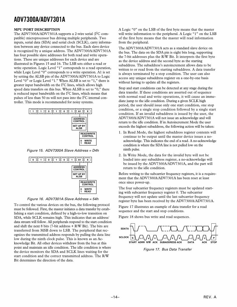
Pin No. Mnemonic Input/Output Function
14–18, 26–30 C0–C9 I 10-Bit Progressive Scan/HDTV Input Port for CrCb color data in 4:2:2 InputMode. In 4:4:4 Input Mode, this input port is used for the Cb (Blue/U) data.The LSBs are set up on Pins C0 and C1. In Default Mode, the input on thisport is output on DAC E.
19 I2C I This input pin must be tied high (VDD_IO) for the ADV7300A/ADV7301A tointerface over the I2C port.
20 ALSB I/O TTL Address Input. This signal sets up the LSB of the MPU address. Whenthis pin is tied low, the I2C filter is activated, which reduces noise on the I2C interface.
21 SDA I/O MPU Port Serial Data Input/Output
22 SCLK I MPU Port Serial Interface Clock Input
23 P_HSYNC I Video Horizontal Sync Control Signal for HD Sync in Simultaneous SD/HDMode and HD Only Mode
24 P_VSYNC I Video Vertical Sync Control Signal for HD Sync in Simultaneous SD/HDMode and HD Only Mode
25 P_BLANK I Video Blanking Control Signal for HD Sync in Simultaneous SD/HD Modeand HD Only Mode
31 RTC_SCR_TR I Multifunctional Input: Realtime Control (RTC) Input, Timing Reset Input,and Subcarrier Reset Input
32 CLKIN_A I Pixel Clock Input for HD Only or SD Only Modes
33 RESET I This input resets the on-chip timing generator and sets the ADV7300A/ADV7301A into default register setting. Reset is an active low signal.
34 EXT_LF I External Loop Filter for the internal PLL
35, 47 RSET2, 1 I A 760 Ω resistor must be connected from this pin to AGND and is used tocontrol the amplitudes of the DAC outputs.
36, 45 COMP2, 1 O Compensation Pin for DACs. Connect 0.1 µF capacitor from COMP pin to VAA.
37 DAC F O In SD Only Mode: Chroma/Red/V Analog Output, in HD Only Mode andSimultaneous HD/SD: Pb/Blue (HD) Analog Output
38 DAC E O In SD Only Mode: Luma/Blue/U Analog Output, in HD Only Mode andSimultaneous HD/SD: Pr/Red (HD) Analog Output
39 DAC D O In SD Only Mode: CVBS/Green/Y Analog Output, in HD Only Mode andSimultaneous HD/SD: Y/Green (HD) Analog Output
40 AGND G Analog Ground
41 VAA P Analog Power Supply
42 DAC C O Chroma/Red/V SD Analog Output
43 DAC B O Luma/Blue/U SD Analog Output
44 DAC A O CVBS/Green/Y SD Analog Output
46 VREF I/O Optional External Voltage Reference Input for DACs or Voltage ReferenceOutput (1.235 V)
48 S_BLANK I/O Video Blanking Control Signal for SD
49 S_VSYNC I/O Video Vertical Control Signal for SD. Option to output SD VSYNC or SDHSYNC in SD Slave Mode 0 and/or any HD Mode.
50 S_HSYNC I/O Video Horizontal Control Signal for SD. Option to output SD HSYNC orHD HSYNC in SD Slave Mode 0 and/or any HD Mode.
51–55, 58–62 S0–S9 I 10-Bit Standard Definition Input Port or Progressive Scan/HDTV Input Portfor Cr (Red/V) color data in 4:4:4 Input Mode. The LSBs are set up on PinsS0 and S1. In Default Mode, the input on this port is output on DAC F.
63 CLKIN_B I Pixel Clock Input. Requires a 27 MHz reference clock for Progressive ScanMode or a 74.25 MHz (74.1758 MHz) reference clock in HDTV Mode. Thisclock input pin is only used in Simultaneous SD/HD Mode.
64 GND_IO Digital Ground
REV. A–14–
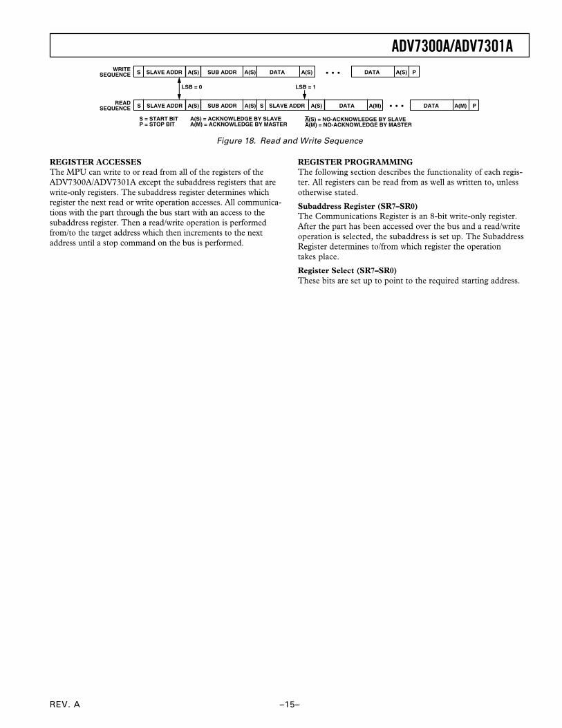
ADV7300A/ADV7301AMPU PORT DESCRIPTIONThe ADV7300A/ADV7301A supports a 2-wire serial (I2C com-patible) microprocessor bus driving multiple peripherals. Twoinputs, serial data (SDA) and serial clock (SCLK), carry informa-tion between any device connected to the bus. Each slave deviceis recognized by a unique address. The ADV7300A/ADV7301Ahas four possible slave addresses for both read and write opera-tions. These are unique addresses for each device and areillustrated in Figures 15 and 16. The LSB sets either a read orwrite operation. Logic Level “1” corresponds to a read operation,while Logic Level “0” corresponds to a write operation. A1 is setby setting the ALSB pin of the ADV7300A/ADV7301A to LogicLevel “0” or Logic Level “1.” When ALSB is set to “1,” there isgreater input bandwidth on the I2C lines, which allows highspeed data transfers on this bus. When ALSB is set to “0,” thereis reduced input bandwidth on the I2C lines, which means thatpulses of less than 50 ns will not pass into the I2C internal con-troller. This mode is recommended for noisy systems.
1 1 0 1 0 1 A1 X
ADDRESSCONTROL
SET UP BYALSB
READ/WRITECONTROL
0 WRITE1 READ
Figure 15. ADV7300A Slave Address = D4h
0 1 0 1 0 1 A1 X
ADDRESSCONTROL
SET UP BYALSB
READ/WRITECONTROL
0 WRITE1 READ
Figure 16. ADV7301A Slave Address = 54h
To control the various devices on the bus, the following protocolmust be followed. First, the master initiates a data transfer by estab-lishing a start condition, defined by a high-to-low transition onSDA, while SCLK remains high. This indicates that an address/data stream will follow. All peripherals respond to the start conditionand shift the next 8 bits (7-bit address + R/W Bit). The bits aretransferred from MSB down to LSB. The peripheral that rec-ognizes the transmitted address responds by pulling the data linelow during the ninth clock pulse. This is known as an Ac-knowledge Bit. All other devices withdraw from the bus at thispoint and maintain an idle condition. The idle condition is wherethe device monitors the SDA and SCLK lines waiting for thestart condition and the correct transmitted address. The R/WBit determines the direction of the data.
A Logic “0” on the LSB of the first byte means that the masterwill write information to the peripheral. A Logic “1” on the LSBof the first byte means that the master will read informationfrom the peripheral.
The ADV7300A/ADV7301A acts as a standard slave device onthe bus. The data on the SDA pin is eight bits long, supportingthe 7-bit addresses plus the R/W Bit. It interprets the first byteas the device address and the second byte as the startingsubaddress. The subaddress’s autoincrement allows data to bewritten to or read from the starting subaddress. A data transferis always terminated by a stop condition. The user can alsoaccess any unique subaddress register on a one-by-one basiswithout having to update all the registers.
Stop and start conditions can be detected at any stage during thedata transfer. If these conditions are asserted out of sequencewith normal read and write operations, it will cause an imme-diate jump to the idle condition. During a given SCLK highperiod, the user should issue only one start condition, one stopcondition, or a single stop condition followed by a single startcondition. If an invalid subaddress is issued by the user, theADV7300A/ADV7301A will not issue an acknowledge and willreturn to the idle condition. If in Autoincrement Mode the userexceeds the highest subaddress, the following action will be taken:
1. In Read Mode, the highest subaddress register contents willcontinue to be output until the master device issues a no-acknowledge. This indicates the end of a read. A no-acknowledgecondition is where the SDA line is not pulled low on theninth pulse.
2. In Write Mode, the data for the invalid byte will not beloaded into any subaddress register, a no-acknowledge willbe issued by the ADV7300A/ADV7301A, and the part willreturn to the idle condition.
Before writing to the subcarrier frequency registers, it is a require-ment that the ADV7300A/ADV7301A has been reset at leastonce since power-up.
The four subcarrier frequency registers must be updated start-ing with subcarrier frequency register 0. The subcarrierfrequency will not update until the last subcarrier frequencyregister byte has been received by the ADV7300A/ADV7301A.
Figure 17 illustrates an example of data transfer for a readsequence and the start and stop conditions.
Figure 18 shows bus write and read sequences.
SDATA
SCLOCK
START ADRR R/W ACK SUBADDRESS ACK DATA ACK STOP
1–7 8 9S 1–7 8 9 1–7 8 9 P
Figure 17. Bus Data Transfer
REV. A
ADV7300A/ADV7301A
–15–
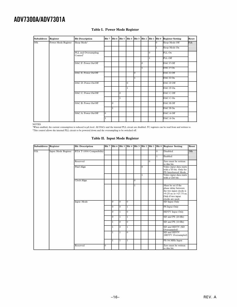
REGISTER ACCESSESThe MPU can write to or read from all of the registers of theADV7300A/ADV7301A except the subaddress registers that arewrite-only registers. The subaddress register determines whichregister the next read or write operation accesses. All communica-tions with the part through the bus start with an access to thesubaddress register. Then a read/write operation is performedfrom/to the target address which then increments to the nextaddress until a stop command on the bus is performed.
REGISTER PROGRAMMINGThe following section describes the functionality of each regis-ter. All registers can be read from as well as written to, unlessotherwise stated.
Subaddress Register (SR7–SR0)The Communications Register is an 8-bit write-only register.After the part has been accessed over the bus and a read/writeoperation is selected, the subaddress is set up. The SubaddressRegister determines to/from which register the operationtakes place.
Register Select (SR7–SR0)These bits are set up to point to the required starting address.
WRITESEQUENCE
READSEQUENCE
S SLAVE ADDR A(S) SUB ADDR A(S) DATA A(S) DATA A(S) P
S SLAVE ADDR A(S) SUB ADDR A(S) S SLAVE ADDR A(S) DATA DATAA(M) A(M) P
S = START BITP = STOP BIT
A(S) = ACKNOWLEDGE BY SLAVEA(M) = ACKNOWLEDGE BY MASTER
A(S) = NO-ACKNOWLEDGE BY SLAVEA(M) = NO-ACKNOWLEDGE BY MASTER
LSB = 0 LSB = 1
Figure 18. Read and Write Sequence
REV. A–16–
ADV7300A/ADV7301ATable I. Power Mode Register
Subaddress Register Bit Description Bit 7 Bit 6 Bit 5 Bit 4 Bit 3 Bit 2 Bit 1 Bit 0 Register Setting Reset
00h Power Mode Register Sleep Mode1 0 Sleep Mode Off
1 Sleep Mode On
PLL and Oversampling Control2
0 PLL On
1 PLL Off
DAC F: Power On/Off 0 DAC F Off
1 DAC F On
DAC E: Power On/Off 0 DAC E Off
1 DAC E On
DAC D: Power On/Off 0 DAC D Off
1 DAC D On
DAC C: Power On/Off 0 DAC C Off
1 DAC C On
DAC B: Power On/Off 0 DAC B Off
1 DAC B On
DAC A: Power On/Off 0 DAC A Off
1 DAC A On
Fch
NOTES1When enabled, the current consumption is reduced to µA level. All DACs and the internal PLL circuit are disabled. I2C registers can be read from and written to.2This control allows the internal PLL circuit to be powered down and the oversampling to be switched off.
Table II. Input Mode Register
Subaddress Register Bit Description Bit 7 Bit 6 Bit 5 Bit 4 Bit 3 Bit 2 Bit 1 Bit 0 Register Setting Reset
01h Input Mode Register 0 Disabled 38h
1 Enabled
Reserved 0 Zero must be written to this bit.
0 Video input data starts with a Y0 bit. Only for PS Interleaved Mode.
1 Video input data starts with a Cb0 bit.
0
1 Must be set if the phase delay between the two input clocks is <9.25 ns or >27.75 ns. Only if two input clocks are used.
0 0 0 SD Input Only
0 0 1 PS Input Only
0 1 0 HDTV Input Only
0 1 1 SD and PS (20-Bit)
1 0 0 SD and PS (10-Bit)
1 0 1 SD and HDTV (SD Oversampled)
1 1 0 SD and HDTV (HDTV Oversampled)
1 1 1 PS 54 MHz Input
Reserved 0 Zero must be written to this bit.
BTA T-1004 Compatibility
Pixel Align
Clock Align
Input Mode
REV. A
ADV7300A/ADV7301A
–17–
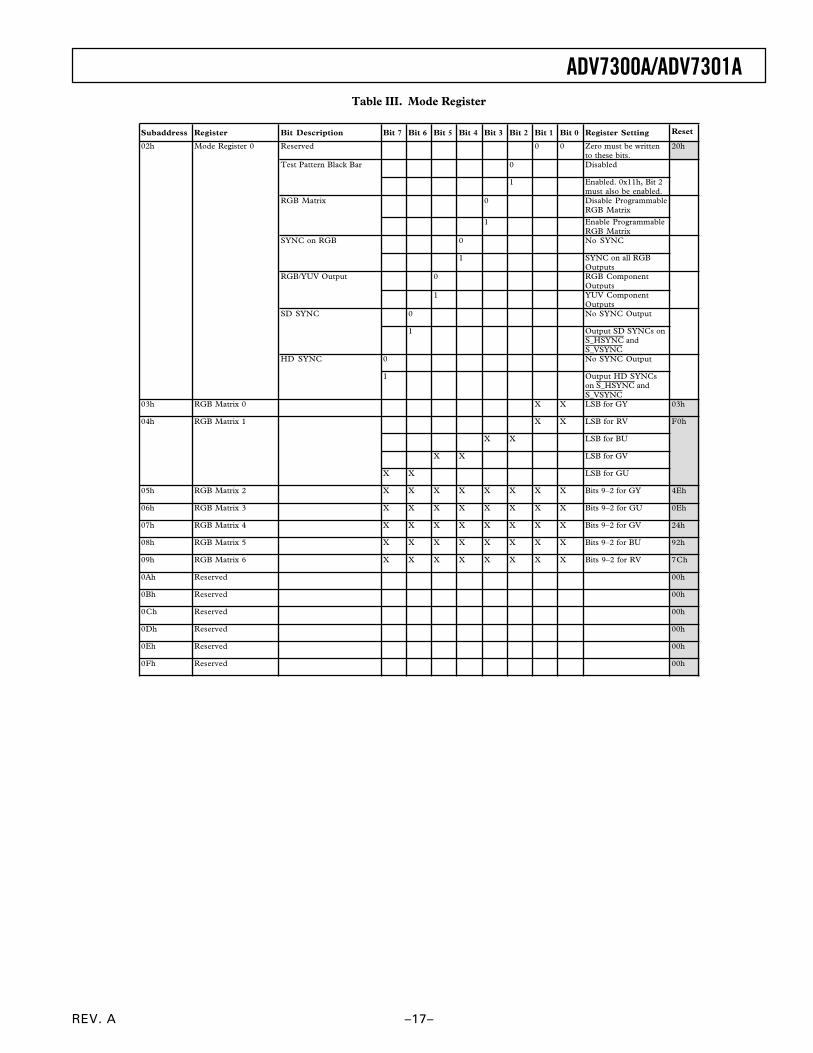
Table III. Mode Register
Subaddress Register Bit Description Bit 7 Bit 6 Bit 5 Bit 4 Bit 3 Bit 2 Bit 1 Bit 0 Register Setting Reset
02h Mode Register 0 Reserved 0 0 Zero must be written to these bits.
20h
0 Disabled
1 Enabled. 0x11h, Bit 2 must also be enabled.
0 Disable Programmable RGB Matrix
1 Enable Programmable RGB Matrix
0 No SYNC
1 SYNC on all RGB Outputs
0 RGB Component Outputs
1 YUV Component Outputs
0 No SYNC Output
1 Output SD SYNCs on S_HSYNC and S_VSYNC
0 No SYNC Output
1 Output HD SYNCs on S_HSYNC and S_VSYNC
03h RGB Matrix 0 X X LSB for GY 03h
04h RGB Matrix 1 X X LSB for RV F0h
X X LSB for BU
X X LSB for GV
X X LSB for GU
05h RGB Matrix 2 X X X X X X X X Bits 9–2 for GY 4Eh
06h RGB Matrix 3 X X X X X X X X Bits 9–2 for GU 0Eh
07h RGB Matrix 4 X X X X X X X X Bits 9–2 for GV 24h
08h RGB Matrix 5 X X X X X X X X Bits 9–2 for BU 92h
09h RGB Matrix 6 X X X X X X X X Bits 9–2 for RV 7Ch
0Ah Reserved 00h
0Bh Reserved 00h
0Ch Reserved 00h
0Dh Reserved 00h
0Eh Reserved 00h
0Fh Reserved 00h
SD SYNC
HD SYNC
Test Pattern Black Bar
RGB Matrix
SYNC on RGB
RGB/YUV Output
REV. A–18–
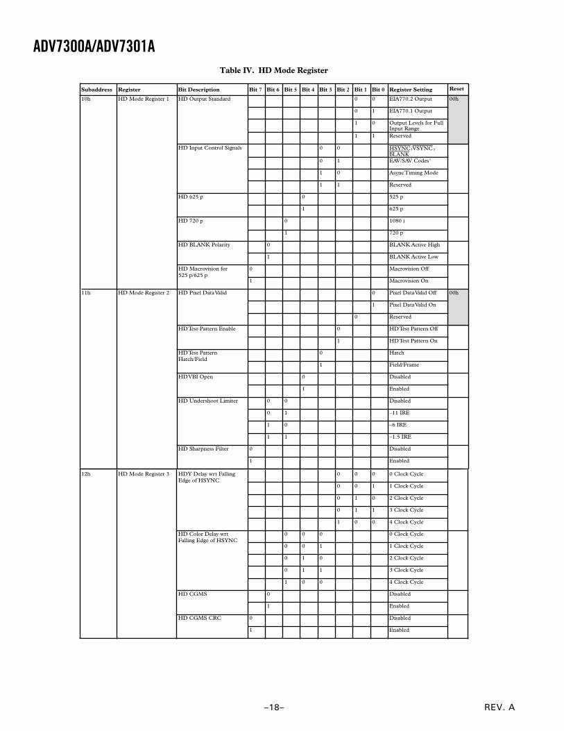
ADV7300A/ADV7301ATable IV. HD Mode Register
Subaddress Register Bit Description Bit 7 Bit 6 Bit 5 Bit 4 Bit 3 Bit 2 Bit 1 Bit 0 Register Setting Reset
10h HD Mode Register 1 0 0 EIA770.2 Output 00h
0 1 EIA770.1 Output
1 0 Output Levels for Full Input Range
1 1 Reserved
0 0 HSYNC VSYNC , BLANK
0 1 EAV/SAV Codes1
1 0 Async Timing Mode
1 1 Reserved
0 525 p
1 625 p
0 1080 i
1 720 p
0 BLANK Active High
1 BLANK Active Low
0 Macrovision Off
1 Macrovision On
11h HD Mode Register 2 0 Pixel Data Valid Off 00h
1 Pixel Data Valid On
0 Reserved
0 HD Test Pattern Off
1 HD Test Pattern On
0 Hatch
1 Field/Frame
0 Disabled
1 Enabled
0 0 Disabled
0 1 –11 IRE
1 0 –6 IRE
1 1 –1.5 IRE
0 Disabled
1 Enabled
HD Undershoot Limiter
HD Sharpness Filter
HD Test Pattern Enable
HD Pixel Data Valid
HD BLANK Polarity
HD Macrovision for 525 p/625 p
HD Test Pattern Hatch/Field
HD VBI Open
HD Input Control Signals
HD Output Standard
HD 625 p
HD 720 p
12h HD Mode Register 3 0 0 0 0 Clock Cycle
0 0 1 1 Clock Cycle
0 1 0 2 Clock Cycle
0 1 1 3 Clock Cycle
1 0 0 4 Clock Cycle
0 0 0 0 Clock Cycle
0 0 1 1 Clock Cycle
0 1 0 2 Clock Cycle
0 1 1 3 Clock Cycle
1 0 0 4 Clock Cycle
0 Disabled
1 Enabled
0 Disabled
1 Enabled
HD Y Delay wrt Falling Edge of HSYNC
HD CGMS
HD CGMS CRC
HD Color Delay wrt Falling Edge of HSYNC
,
REV. A
ADV7300A/ADV7301A
–19–
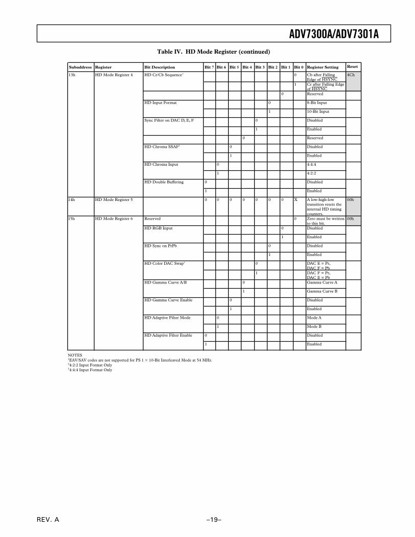
Table IV. HD Mode Register (continued)
Subaddress Register Bit Description Bit 7 Bit 6 Bit 5 Bit 4 Bit 3 Bit 2 Bit 1 Bit 0 Register Setting Reset
13h HD Mode Register 4 0 Cb after Falling Edge of HSYNC
1 Cr after Falling Edge of HSYNC
0 Reserved
0 8-Bit Input
1 10-Bit Input
0 Disabled
1 Enabled
0 Reserved
HD Chroma SSAF2 0 Disabled
1 Enabled
HD Chroma Input 0 4:4:4
1 4:2:2
HD Double Buffering 0 Disabled
1 Enabled
14h HD Mode Register 5 0 0 0 0 0 0 0 X A low-high-low transition resets the internal HD timing counters.
00h
15h HD Mode Register 6 Reserved 0 Zero must be written to this bit.
00h
HD RGB Input 0 Disabled
1 Enabled
HD Sync on PrPb 0 Disabled
1 Enabled
HD Color DAC Swap3 0 DAC E = Pr, DAC F = Pb
1 DAC F = Pr, DAC E = Pb
HD Gamma Curve A/B 0 Gamma Curve A
1 Gamma Curve B
HD Gamma Curve Enable 0 Disabled
1 Enabled
HD Adaptive Filter Mode 0 Mode A
1 Mode B
HD Adaptive Filter Enable 0 Disabled
1 Enabled
4Ch
Sync Filter on DAC D, E, F
HD Input Format
HD Cr/Cb Sequence2
NOTES1EAV/SAV codes are not supported for PS 1 10-Bit Interleaved Mode at 54 MHz.24:2:2 Input Format Only34:4:4 Input Format Only
REV. A–20–
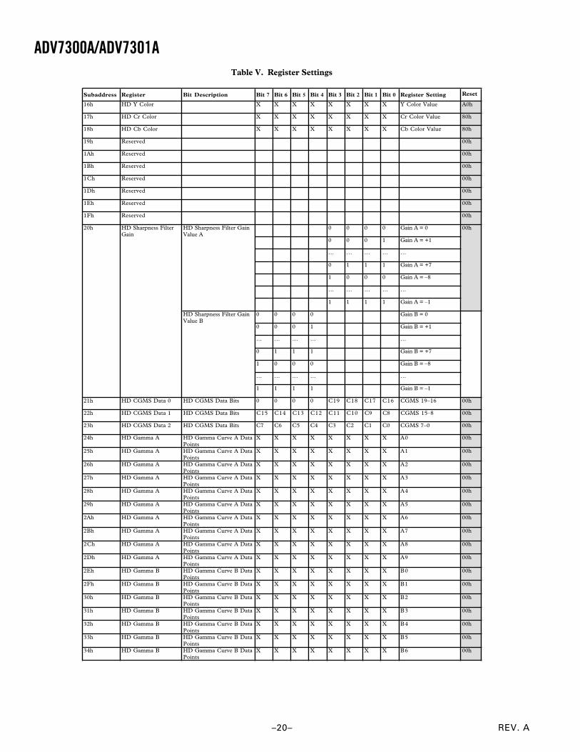
ADV7300A/ADV7301ATable V. Register Settings
Subaddress Register Bit Description Bit 7 Bit 6 Bit 5 Bit 4 Bit 3 Bit 2 Bit 1 Bit 0 Register Setting Reset
16h HD Y Color X X X X X X X X Y Color Value A0h
17h HD Cr Color X X X X X X X X Cr Color Value 80h
18h HD Cb Color X X X X X X X X Cb Color Value 80h
19h Reserved 00h
1Ah Reserved 00h
1Bh Reserved 00h
1Ch Reserved 00h
1Dh Reserved 00h
1Eh Reserved 00h
1Fh Reserved 00h
20h 0 0 0 0 Gain A = 0
0 0 0 1 Gain A = +1
… … … … …
0 1 1 1 Gain A = +7
1 0 0 0 Gain A = –8
… … … … …
1 1 1 1 Gain A = –1
0 0 0 0 Gain B = 0
0 0 0 1 Gain B = +1
… … … … …
0 1 1 1 Gain B = +7
1 0 0 0 Gain B = –8
… … … … …
1 1 1 1 Gain B = –1
21h HD CGMS Data 0 HD CGMS Data Bits 0 0 0 0 C19 C18 C17 C16 CGMS 19–16 00h
22h HD CGMS Data 1 HD CGMS Data Bits C15 C14 C13 C12 C11 C10 C9 C8 CGMS 15–8 00h
23h HD CGMS Data 2 HD CGMS Data Bits C7 C6 C5 C4 C3 C2 C1 C0 CGMS 7–0 00h
24h HD Gamma A HD Gamma Curve A Data Points
X X X X X X X X A0 00h
25h HD Gamma A HD Gamma Curve A Data Points
X X X X X X X X A1 00h
26h HD Gamma A HD Gamma Curve A Data Points
X X X X X X X X A2 00h
27h HD Gamma A HD Gamma Curve A Data Points
X X X X X X X X A3 00h
28h HD Gamma A HD Gamma Curve A Data Points
X X X X X X X X A4 00h
29h HD Gamma A HD Gamma Curve A Data Points
X X X X X X X X A5 00h
2Ah HD Gamma A HD Gamma Curve A Data Points
X X X X X X X X A6 00h
2Bh HD Gamma A HD Gamma Curve A Data Points
X X X X X X X X A7 00h
2Ch HD Gamma A HD Gamma Curve A Data Points
X X X X X X X X A8 00h
2Dh HD Gamma A HD Gamma Curve A Data Points
X X X X X X X X A9 00h
2Eh HD Gamma B HD Gamma Curve B Data Points
X X X X X X X X B0 00h
2Fh HD Gamma B HD Gamma Curve B Data Points
X X X X X X X X B1 00h
30h HD Gamma B HD Gamma Curve B Data Points
X X X X X X X X B2 00h
31h HD Gamma B HD Gamma Curve B Data Points
X X X X X X X X B3 00h
32h HD Gamma B HD Gamma Curve B Data Points
X X X X X X X X B4 00h
33h HD Gamma B HD Gamma Curve B Data Points
X X X X X X X X B5 00h
34h HD Gamma B HD Gamma Curve B Data Points
X X X X X X X X B6 00h
HD Sharpness Filter Gain
HD Sharpness Filter Gain Value A
HD Sharpness Filter Gain Value B
00h
REV. A
ADV7300A/ADV7301A
–21–
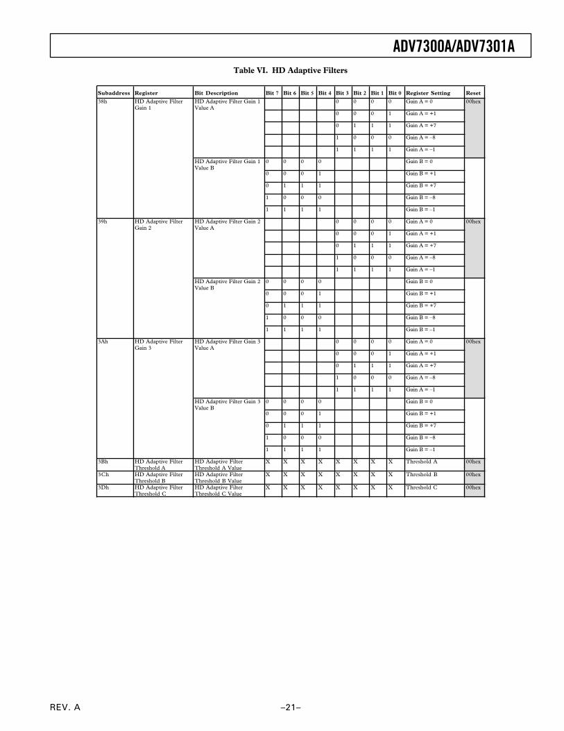
Table VI. HD Adaptive Filters
Subaddress Register Bit Description Bit 7 Bit 6 Bit 5 Bit 4 Bit 3 Bit 2 Bit 1 Bit 0 Register Setting Reset
38h 0 0 0 0 Gain A = 0
0 0 0 1 Gain A = +1
0 1 1 1 Gain A = +7
1 0 0 0 Gain A = –8
1 1 1 1 Gain A = –1
0 0 0 0 Gain B = 0
0 0 0 1 Gain B = +1
0 1 1 1 Gain B = +7
1 0 0 0 Gain B = –8
1 1 1 1 Gain B = –1
39h 0 0 0 0 Gain A = 0
0 0 0 1 Gain A = +1
0 1 1 1 Gain A = +7
1 0 0 0 Gain A = –8
1 1 1 1 Gain A = –1
0 0 0 0 Gain B = 0
0 0 0 1 Gain B = +1
0 1 1 1 Gain B = +7
1 0 0 0 Gain B = –8
1 1 1 1 Gain B = –1
3Ah 0 0 0 0 Gain A = 0
0 0 0 1 Gain A = +1
0 1 1 1 Gain A = +7
1 0 0 0 Gain A = –8
1 1 1 1 Gain A = –1
0 0 0 0 Gain B = 0
0 0 0 1 Gain B = +1
0 1 1 1 Gain B = +7
1 0 0 0 Gain B = –8
1 1 1 1 Gain B = –1
3Bh HD Adaptive Filter Threshold A
HD Adaptive Filter Threshold A Value
X X X X X X X X Threshold A 00hex
3Ch HD Adaptive Filter Threshold B
HD Adaptive Filter Threshold B Value
X X X X X X X X Threshold B 00hex
3Dh HD Adaptive Filter Threshold C
HD Adaptive Filter Threshold C Value
X X X X X X X X Threshold C 00hex
HD Adaptive Filter Gain 3 Value B
HD Adaptive Filter Gain 2 Value A
HD Adaptive Filter Gain 2 Value B
HD Adaptive Filter Gain 1
HD Adaptive Filter Gain 2
HD Adaptive Filter Gain 3
00hex
00hex
00hex
HD Adaptive Filter Gain 1 Value B
HD Adaptive Filter Gain 1 Value A
HD Adaptive Filter Gain 3 Value A
REV. A–22–
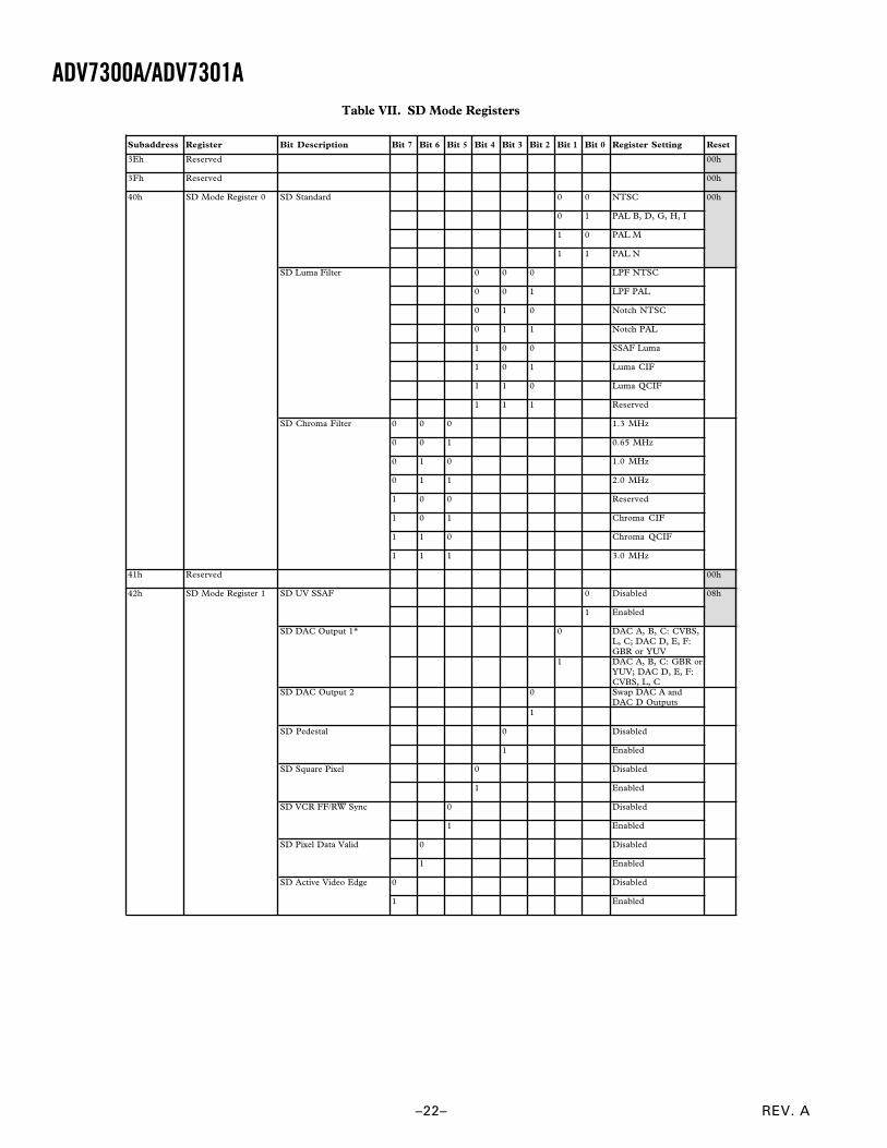
ADV7300A/ADV7301ATable VII. SD Mode Registers
Subaddress Register Bit Description Bit 7 Bit 6 Bit 5 Bit 4 Bit 3 Bit 2 Bit 1 Bit 0 Register Setting Reset
3Eh Reserved 00h
3Fh Reserved 00h
40h SD Mode Register 0 0 0 NTSC
0 1 PAL B, D, G, H, I
1 0 PAL M
1 1 PAL N
0 0 0 LPF NTSC
0 0 1 LPF PAL
0 1 0 Notch NTSC
0 1 1 Notch PAL
1 0 0 SSAF Luma
1 0 1 Luma CIF
1 1 0 Luma QCIF
1 1 1 Reserved
0 0 0 1.3 MHz
0 0 1 0.65 MHz
0 1 0 1.0 MHz
0 1 1 2.0 MHz
1 0 0 Reserved
1 0 1 Chroma CIF
1 1 0 Chroma QCIF
1 1 1 3.0 MHz
41h Reserved 00h
42h SD Mode Register 1 0 Disabled
1 Enabled
0 DAC A, B, C: CVBS, L, C; DAC D, E, F: GBR or YUV
1 DAC A, B, C: GBR or YUV; DAC D, E, F: CVBS, L, C
0 Swap DAC A and DAC D Outputs
1
0 Disabled
1 Enabled
0 Disabled
1 Enabled
0 Disabled
1 Enabled
0 Disabled
1 Enabled
0 Disabled
1 Enabled
00h
08h
SD Pixel Data Valid
SD Active Video Edge
SD Pedestal
SD Square Pixel
SD VCR FF/RW Sync
SD Standard
SD Luma Filter
SD Chroma Filter
SD DAC Output 2
SD UV SSAF
SD DAC Output 1*
REV. A
ADV7300A/ADV7301A
–23–
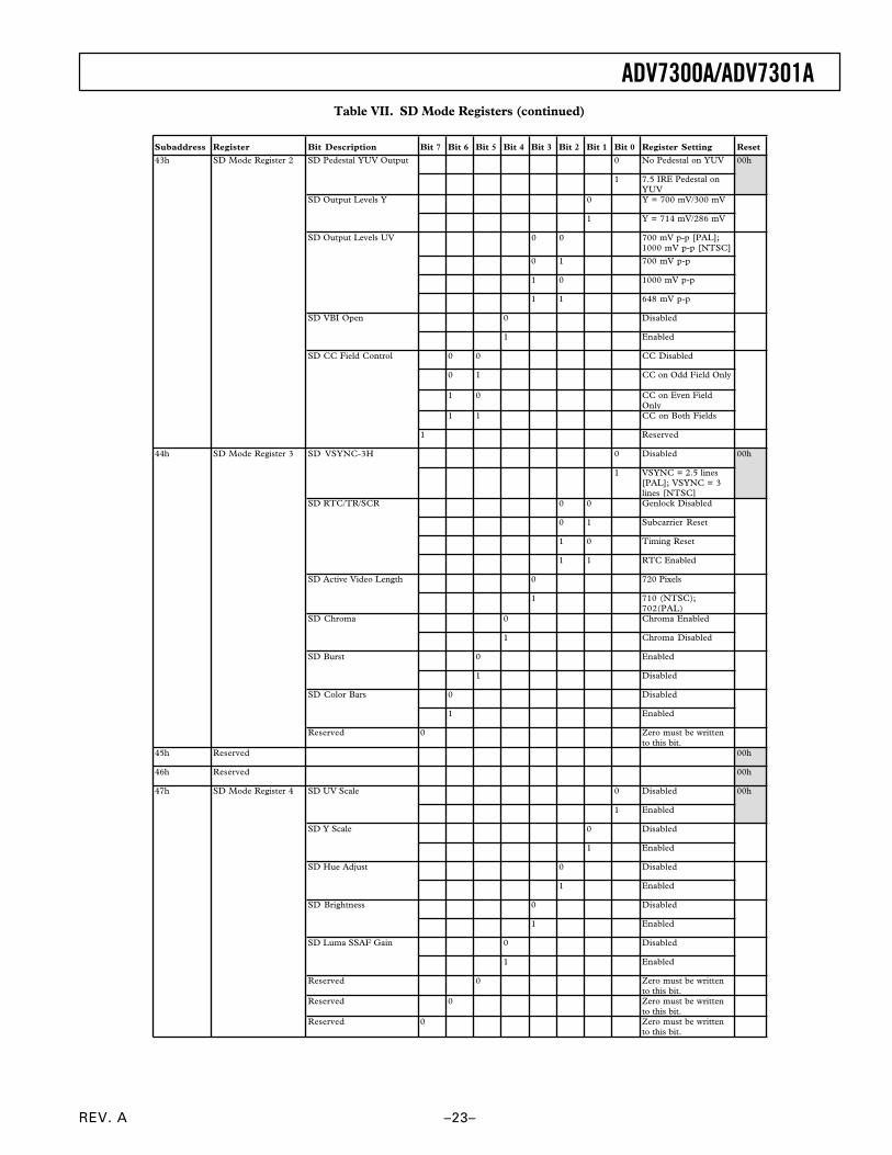
Table VII. SD Mode Registers (continued)
Subaddress Register Bit Description Bit 7 Bit 6 Bit 5 Bit 4 Bit 3 Bit 2 Bit 1 Bit 0 Register Setting Reset
43h SD Mode Register 2 SD Pedestal YUV Output 0 No Pedestal on YUV
1 7.5 IRE Pedestal on YUV
SD Output Levels Y 0 Y = 700 mV/300 mV
1 Y = 714 mV/286 mV
SD Output Levels UV 0 0 700 mV p-p [PAL]; 1000 mV p-p [NTSC]
0 1 700 mV p-p
1 0 1000 mV p-p
1 1 648 mV p-p
SD VBI Open 0 Disabled
1 Enabled
0 0 CC Disabled
0 1 CC on Odd Field Only
1 0 CC on Even Field Only
1 1 CC on Both Fields
1 Reserved
0 Disabled
1 VSYNC = 2.5 lines [PAL]; VSYNC = 3 lines [NTSC]
0 0 Genlock Disabled
0 1 Subcarrier Reset
1 0 Timing Reset
1 1 RTC Enabled
0 720 Pixels
1 710 (NTSC); 702(PAL)
0 Chroma Enabled
1 Chroma Disabled
0 Enabled
1 Disabled
0 Disabled
1 Enabled
Reserved 0 Zero must be written to this bit.
45h Reserved 00h
46h Reserved 00h
0 Disabled
1 Enabled
0 Disabled
1 Enabled
0 Disabled
1 Enabled
0 Disabled
1 Enabled
0 Disabled
1 Enabled
Reserved 0 Zero must be written to this bit.
Reserved 0 Zero must be written to this bit.
Reserved 0 Zero must be written to this bit.
00h
SD Mode Register 3
SD RTC/TR/SCR
SD VSYNC-3H 00h
00hSD Mode Register 447h
SD Luma SSAF Gain
SD Brightness
SD Hue Adjust
SD Y Scale
SD UV Scale
SD CC Field Control
44h
SD Active Video Length
SD Chroma
SD Burst
SD Color Bars
REV. A–24–
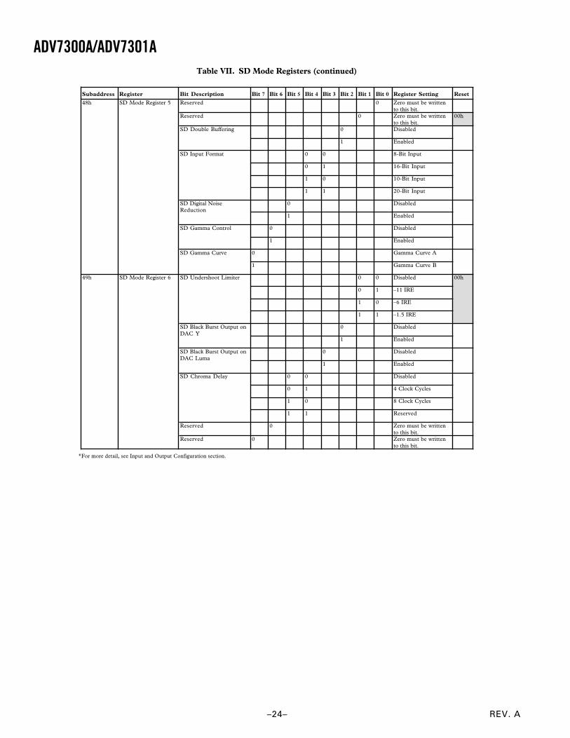
ADV7300A/ADV7301ATable VII. SD Mode Registers (continued)
Subaddress Register Bit Description Bit 7 Bit 6 Bit 5 Bit 4 Bit 3 Bit 2 Bit 1 Bit 0 Register Setting Reset
Reserved 0 Zero must be written to this bit.
Reserved 0 Zero must be written to this bit.
00h
0 Disabled
1 Enabled
0 0 8-Bit Input
0 1 16-Bit Input
1 0 10-Bit Input
1 1 20-Bit Input
0 Disabled
1 Enabled
0 Disabled
1 Enabled
0 Gamma Curve A
1 Gamma Curve B
0 0 Disabled
0 1 –11 IRE
1 0 –6 IRE
1 1 –1.5 IRE
0 Disabled
1 Enabled
0 Disabled
1 Enabled
0 0 Disabled
0 1 4 Clock Cycles
1 0 8 Clock Cycles
1 1 Reserved
Reserved 0 Zero must be written to this bit.
Reserved 0 Zero must be written to this bit.
SD Double Buffering
SD Mode Register 548h
SD Gamma Control
SD Gamma Curve
SD Digital Noise Reduction
SD Input Format
00h49h SD Mode Register 6 SD Undershoot Limiter
SD Black Burst Output on DAC Y
SD Chroma Delay
SD Black Burst Output on DAC Luma
*For more detail, see Input and Output Configuration section.
REV. A
ADV7300A/ADV7301A
–25–
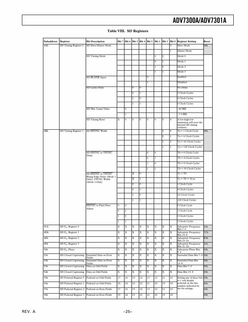
Table VIII. SD Registers
Subaddress Register Bit Description Bit 7 Bit 6 Bit 5 Bit 4 Bit 3 Bit 2 Bit 1 Bit 0 Register Setting Reset
4Ah SD Timing Register 0 SD Slave/Master Mode 0 Slave Mode
1 Master Mode
SD Timing Mode 0 0 Mode 0
0 1 Mode 1
1 0 Mode 2
1 1 Mode 3
SD BLANK Input 0 Enabled
1 Disabled
SD Luma Delay 0 0 No Delay
0 1 2 Clock Cycles
1 0 4 Clock Cycles
1 1 6 Clock Cycles
SD Min. Luma Value 0 –40 IRE
1 –7.5 IRE
SD Timing Reset X 0 0 0 0 0 0 0 A low-high-low transistion will reset the internal SD timing counters.
4Bh SD Timing Register 1 0 0 Ta = 1 Clock Cycle
0 1 Ta = 4 Clock Cycles
1 0 Ta = 16 Clock Cycles
1 1 Ta = 128 Clock Cycles
0 0 Tb = 0 Clock Cycle
0 1 Tb = 4 Clock Cycles
1 0 Tb = 8 Clock Cycles
1 1 Tb = 18 Clock Cycles
X 0 Tc = Tb
X 1 Tc = Tb + 32 µs
0 0 1 Clock Cycle
0 1 4 Clock Cycles
1 0 16 Clock Cycles
1 1 128 Clock Cycles
0 0 0 Clock Cycle
0 1 1 Clock Cycle
1 0 2 Clock Cycles
1 1 3 Clock Cycles
4Ch SD FSC Register 0 X X X X X X X X Subcarrier Frequency Bits 7–0
16h
4Dh SD FSC Register 1 X X X X X X X X Subcarrier Frequency Bits 15–8
7Ch
4Eh SD FSC Register 2 X X X X X X X X Subcarrier Frequency Bits 23–16
F0h
4Fh SD FSC Register 3 X X X X X X X X Subcarrier Frequency Bits 31–24
21h
50h SD FSC Phase X X X X X X X X Subcarrier Phase Bits 9–2
00h
51h SD Closed Captioning Extended Data on Even Fields
X X X X X X X X Extended Data Bits 7–0 00h
52h SD Closed Captioning Extended Data on Even Fields
X X X X X X X X Extended Data Bits 15–8
00h
53h SD Closed Captioning Data on Odd Fields X X X X X X X X Data Bits 7–0 00h
54h SD Closed Captioning Data on Odd Fields X X X X X X X X Data Bits 15–8 00h
55h SD Pedestal Register 0 Pedestal on Odd Fields 17 16 15 14 13 12 11 10 00h
56h SD Pedestal Register 1 Pedestal on Odd Fields 25 24 23 22 21 20 19 18 00h
57h SD Pedestal Register 2 Pedestal on Even Fields 17 16 15 14 13 12 11 10 00h
58h SD Pedestal Register 3 Pedestal on Even Fields 25 24 23 22 21 20 19 18 00h
Setting any of these bits to 1 will disable pedestal on the line number indicated by the bit settings.
08h
00h
SD HSYNC to VSYNC Delay
HSYNC to Pixel Data Adjust
SD HSYNC to VSYNC Rising Edge Delay (Mode 1 Only); VSYNC Width (Mode 2 Only)
SD HSYNC Width
REV. A–26–
ADV7300A/ADV7301ATable VIII. SD Registers (continued)
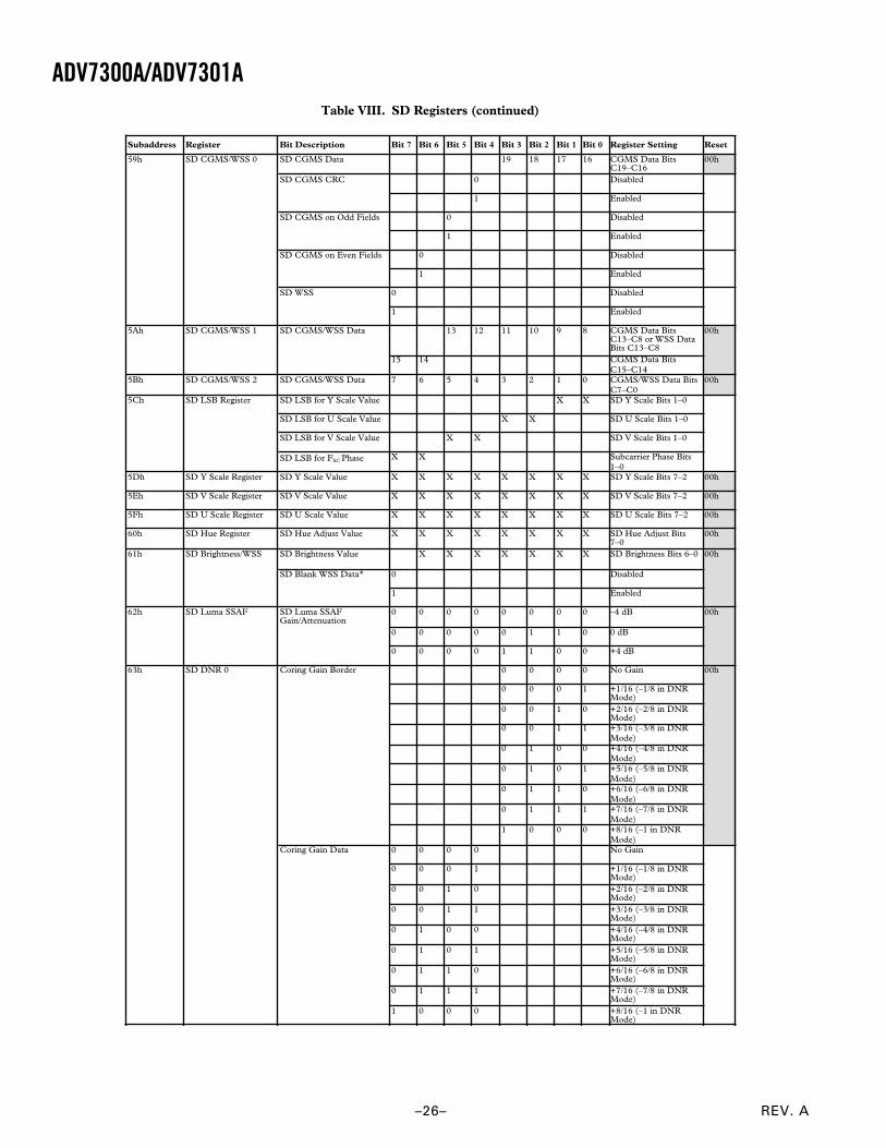
Subaddress Register Bit Description Bit 7 Bit 6 Bit 5 Bit 4 Bit 3 Bit 2 Bit 1 Bit 0 Register Setting Reset
59h SD CGMS/WSS 0 SD CGMS Data 19 18 17 16 CGMS Data Bits C19–C16
00h
SD CGMS CRC 0 Disabled
1 Enabled
SD CGMS on Odd Fields 0 Disabled
1 Enabled
SD CGMS on Even Fields 0 Disabled
1 Enabled
SD WSS 0 Disabled
1 Enabled
5Ah SD CGMS/WSS 1 SD CGMS/WSS Data 13 12 11 10 9 8 CGMS Data Bits C13–C8 or WSS Data Bits C13–C8
00h
15 14 CGMS Data Bits C15–C14
5Bh SD CGMS/WSS 2 SD CGMS/WSS Data 7 6 5 4 3 2 1 0 CGMS/WSS Data Bits C7–C0
00h
5Ch SD LSB Register SD LSB for Y Scale Value X X SD Y Scale Bits 1–0
SD LSB for U Scale Value X X SD U Scale Bits 1–0
SD LSB for V Scale Value X X SD V Scale Bits 1–0
SD LSB for FSC Phase X X Subcarrier Phase Bits 1–0
5Dh SD Y Scale Register SD Y Scale Value X X X X X X X X SD Y Scale Bits 7–2 00h
5Eh SD V Scale Register SD V Scale Value X X X X X X X X SD V Scale Bits 7–2 00h
5Fh SD U Scale Register SD U Scale Value X X X X X X X X SD U Scale Bits 7–2 00h
60h SD Hue Register SD Hue Adjust Value X X X X X X X X SD Hue Adjust Bits 7–0
00h
61h SD Brightness/WSS SD Brightness Value X X X X X X X SD Brightness Bits 6–0
SD Blank WSS Data* 0 Disabled
1 Enabled
62h SD Luma SSAF SD Luma SSAF Gain/Attenuation
0 0 0 0 0 0 0 0 –4 dB
0 0 0 0 0 1 1 0 0 dB
0 0 0 0 1 1 0 0 +4 dB
63h SD DNR 0 Coring Gain Border 0 0 0 0 No Gain
0 0 0 1 +1/16 (–1/8 in DNR Mode)
0 0 1 0 +2/16 (–2/8 in DNR Mode)
0 0 1 1 +3/16 (–3/8 in DNR Mode)
0 1 0 0 +4/16 (–4/8 in DNR Mode)
0 1 0 1 +5/16 (–5/8 in DNR Mode)
0 1 1 0 +6/16 (–6/8 in DNR Mode)
0 1 1 1 +7/16 (–7/8 in DNR Mode)
1 0 0 0 +8/16 (–1 in DNR Mode)
Coring Gain Data 0 0 0 0 No Gain
0 0 0 1 +1/16 (–1/8 in DNR Mode)
0 0 1 0 +2/16 (–2/8 in DNR Mode)
0 0 1 1 +3/16 (–3/8 in DNR Mode)
0 1 0 0 +4/16 (–4/8 in DNR Mode)
0 1 0 1 +5/16 (–5/8 in DNR Mode)
0 1 1 0 +6/16 (–6/8 in DNR Mode)
0 1 1 1 +7/16 (–7/8 in DNR Mode)
1 0 0 0 +8/16 (–1 in DNR Mode)
00h
00h
00h
REV. A
ADV7300A/ADV7301A
–27–
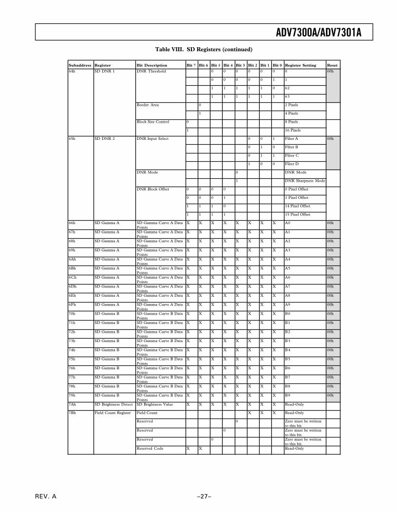
Table VIII. SD Registers (continued)
Subaddress Register Bit Description Bit 7 Bit 6 Bit 5 Bit 4 Bit 3 Bit 2 Bit 1 Bit 0 Register Setting Reset
64h SD DNR 1 DNR Threshold 0 0 0 0 0 0 0
0 0 0 0 0 1 1
1 1 1 1 1 0 62
1 1 1 1 1 1 63
Border Area 0 2 Pixels
1 4 Pixels
Block Size Control 0 8 Pixels
1 16 Pixels
0 0 1 Filter A
0 1 0 Filter B
0 1 1 Filter C
1 0 0 Filter D
0 DNR Mode
1 DNR Sharpness Mode
0 0 0 0 0 Pixel Offset
0 0 0 1 1 Pixel Offset
1 1 1 0 14 Pixel Offset
1 1 1 1 15 Pixel Offset
66h SD Gamma A SD Gamma Curve A Data Points
X X X X X X X X A0 00h
67h SD Gamma A SD Gamma Curve A Data Points
X X X X X X X X A1 00h
68h SD Gamma A SD Gamma Curve A Data Points
X X X X X X X X A2 00h
69h SD Gamma A SD Gamma Curve A Data Points
X X X X X X X X A3 00h
6Ah SD Gamma A SD Gamma Curve A Data Points
X X X X X X X X A4 00h
6Bh SD Gamma A SD Gamma Curve A Data Points
X X X X X X X X A5 00h
6Ch SD Gamma A SD Gamma Curve A Data Points
X X X X X X X X A6 00h
6Dh SD Gamma A SD Gamma Curve A Data Points
X X X X X X X X A7 00h
6Eh SD Gamma A SD Gamma Curve A Data Points
X X X X X X X X A8 00h
6Fh SD Gamma A SD Gamma Curve A Data Points
X X X X X X X X A9 00h
70h SD Gamma B SD Gamma Curve B Data Points
X X X X X X X X B0 00h
71h SD Gamma B SD Gamma Curve B Data Points
X X X X X X X X B1 00h
72h SD Gamma B SD Gamma Curve B Data Points
X X X X X X X X B2 00h
73h SD Gamma B SD Gamma Curve B Data Points
X X X X X X X X B3 00h
74h SD Gamma B SD Gamma Curve B Data Points
X X X X X X X X B4 00h
75h SD Gamma B SD Gamma Curve B Data Points
X X X X X X X X B5 00h
76h SD Gamma B SD Gamma Curve B Data Points
X X X X X X X X B6 00h
77h SD Gamma B SD Gamma Curve B Data Points
X X X X X X X X B7 00h
78h SD Gamma B SD Gamma Curve B Data Points
X X X X X X X X B8 00h
79h SD Gamma B SD Gamma Curve B Data Points
X X X X X X X X B9 00h
7Ah SD Brightness Detect SD Brightness Value X X X X X X X X Read-Only
7Bh Field Count Register Field Count X X X Read-Only
Reserved 0 Zero must be written to this bit.
Reserved 0 Zero must be written to this bit.
Reserved 0 Zero must be written to this bit.
Reserved Code X X Read-Only
DNR Block Offset
SD DNR 265h
00h
00hDNR Input Select
DNR Mode
REV. A–28–
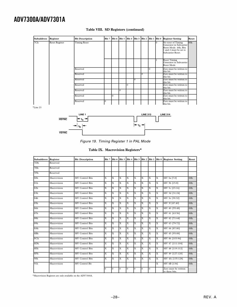
ADV7300A/ADV7301ATable VIII. SD Registers (continued)
Subaddress Register Bit Description Bit 7 Bit 6 Bit 5 Bit 4 Bit 3 Bit 2 Bit 1 Bit 0 Register Setting Reset
7Ch Reset Register Timing Reset 0 No reset of Timing Generator in Subcarrier Reset Mode. 44h, Bits 1 and 2 must be set to Subcarrier Reset.
1 Reset Timing Generator in Subcarrier Reset Mode
Reserved 0 Zero must be written to this bit.
Reserved 0 Zero must be written to this bit.
Reserved 0 Zero must be written to this bit.
Reserved 0 Zero must be written to this bit.
Reserved 0 Zero must be written to this bit.
Reserved 0 Zero must be written to this bit.
Reserved 0 Zero must be written to this bit.
00h
*Line 23
LINE 313 LINE 314LINE 1
tB
HSYNC
VSYNC
tA
tC
Figure 19. Timing Register 1 in PAL Mode
Table IX. Macrovision Registers*
Subaddress Register Bit Description Bit 7 Bit 6 Bit 5 Bit 4 Bit 3 Bit 2 Bit 1 Bit 0 Register Setting Reset
7Dh Reserved
7Eh Reserved
7Fh Reserved
80h Macrovision MV Control Bits X X X X X X X X MV 3a [7:0] 00h
81h Macrovision MV Control Bits X X X X X X X X MV 3b [15:8] 00h
82h Macrovision MV Control Bits X X X X X X X X MV 3c [23:16] 00h
83h Macrovision MV Control Bits X X X X X X X X MV 3d [31:24] 00h
84h Macrovision MV Control Bits X X X X X X X X MV 3e [39:32] 00h
85h Macrovision MV Control Bits X X X X X X X X MV 3f [47:40] 00h
86h Macrovision MV Control Bits X X X X X X X X MV 40 [55:48] 00h
87h Macrovision MV Control Bits X X X X X X X X MV 41 [63:56] 00h
88h Macrovision MV Control Bits X X X X X X X X MV 42 [71:64] 00h
89h Macrovision MV Control Bits X X X X X X X X MV 43 [79:72] 00h
8Ah Macrovision MV Control Bits X X X X X X X X MV 44 [87:80] 00h
8Bh Macrovision MV Control Bits X X X X X X X X MV 45 [95:88] 00h
8Ch Macrovision MV Control Bits X X X X X X X X MV 46 [103:96] 00h
8Dh Macrovision MV Control Bits X X X X X X X X MV 47 [111:104] 00h
8Eh Macrovision MV Control Bits X X X X X X X X MV 48 [119:112] 00h
8Fh Macrovision MV Control Bits X X X X X X X X MV 49 [127:120] 00h
90h Macrovision MV Control Bits X X X X X X X X MV 4A [135:128] 00h
X MV 4B [136]
0 0 0 0 0 0 0 Zero must be written to these bits.
MV Control BitMacrovision91h 00h
*Macrovision Registers are only available on the ADV7300A.
REV. A
ADV7300A/ADV7301A
–29–
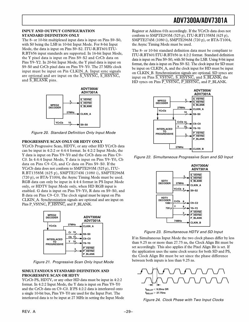
INPUT AND OUTPUT CONFIGURATIONSTANDARD DEFINITION ONLYThe 8- or 10-bit multiplexed input data is input on Pins S9–S0,with S0 being the LSB in 10-bit Input Mode. For 8-bit InputMode, the data is input on Pins S9–S2. ITU-R.BT601/ITU-R.BT656 input standards are supported. In 16-bit Input Mode,the Y pixel data is input on Pins S9–S2 and CrCb data onPins Y9–Y2. In 20-bit Input Mode, the Y pixel data is input onS9–S0 and CrCb pixel data on Pins Y9–Y0. The 27 MHz clockinput must be input on Pin CLKIN_A. Input sync signalsare optional and are input on the S_VSYNC, S_HSYNC,and S_BLANK pins.
MPEG2DECODER
S_VSYNCS_HSYNCS_BLANK
CLKIN_A
S9–S0
27MHz
3
10YCrCb
ADV7300A/ADV7301A
Figure 20. Standard Definition Only Input Mode
PROGRESSIVE SCAN ONLY OR HDTV ONLYYCrCb Progressive Scan, HDTV, or any other HD YCrCb datacan be input in 4:2:2 or 4:4:4 format. In 4:2:2 Input Mode, theY data is input on Pins Y9–Y0 and the CrCb data on Pins C9–C0. In 4:4:4 Input Mode, Y data is input on Pins Y9–Y0, Cbdata on Pins C9–C0, and Cr data on Pins S9–S0. If theYCrCb data does not conform to SMPTE293M (525 p), ITU-R.BT1358M (625 p), SMPTE274M (1080 i), SMPTE296M(720 p), or BTA-T1004, the Async Timing Mode must be used.RGB data can only be input in 4:4:4 format in PS Input Modeonly, or HDTV Input Mode only, when HD RGB input isenabled. G data is input on Pins Y9–Y0, R data on S9–S0, andB data on Pins C9–C0. The clock signal must be input on PinCLKIN_A. Synchronization signals are optional and are input onPins P_VSYNC, P_HSYNC, and P_BLANK.
MPEG2DECODER
P_VSYNCP_HSYNCP_BLANK
CLKIN_A
S9–S010Cr
C9–C0
Y9–Y0
INTERLACEDTO
PROGRESSIVE
YCrCb
10Cb
10Y
3
27MHz
ADV7300A/ADV7301A
Figure 21. Progressive Scan Only Input Mode
SIMULTANEOUS STANDARD DEFINITION ANDPROGRESSIVE SCAN OR HDTVYCrCb PS, HDTV, or any other HD data must be input in 4:2:2format. In 4:2:2 Input Mode, the Y data is input on Pins Y9–Y0and the CrCb data on C9–C0. If PS 4:2:2 data is interleaved ontoa single 10-bit bus, Pins Y9–Y0 are used for the Input Port. Theinterleaved data is to be input at 27 MHz in setting the Input Mode
Register at Address 01h accordingly. If the YCrCb data does notconform to SMPTE293M (525 p), ITU-R.BT1358M (625 p),SMPTE274M (1080 i), SMPTE296M (720 p), or BTA-T1004,the Async Timing Mode must be used.
The 8- or 10-bit standard definition data must be compliant toITU-R.BT601/ITU-R.BT656 in 4:2:2 format. Standard definitiondata is input on Pins S9–S0, with S0 being the LSB. Using 8-bit inputformat, the data is input on Pins S9–S2. The clock input for SD mustbe input on CLKIN_A, and the clock input for HD must be inputon CLKIN_B. Synchronization signals are optional. SD syncs areinput on Pins S_VSYNC, S_HSYNC, and S_BLANK; theHD syncs on Pins P_VSYNC, P_HSYNC, and P_BLANK.
MPEG2DECODER
S_VSYNCS_HSYNCS_BLANK
CLKIN_A
C9–C010CrCb
Y9–Y0INTERLACEDTO
PROGRESSIVE
YCrCb
10Y
3P_VSYNCP_HSYNCP_BLANK
CLKIN_B
3
27MHz
S9–S010
27MHz
ADV7300A/ADV7301A
Figure 22. Simultaneous Progressive Scan and SD Input
S_VSYNCS_HSYNCS_BLANK
CLKIN_A
P_VSYNCP_HSYNCP_BLANK
CLKIN_B
SDTVDECODER
3
27MHz
8YCrCb
HDTVDECODER 8CrCb
8Y
3
74MHz
1080 i
720 p
ADV7300A/ADV7301A
S9–S2
C9–C2
Y9–Y2
Figure 23. Simultaneous HDTV and SD Input
If in Simultaneous Input Mode the two clock phases differ by lessthan 9.25 ns or more than 27.75 ns, the Clock Align Bit must beset accordingly. This also applies if the Pixel Align Bit is set. Ifthe application uses the same clock source for both SD and PS,the Clock Align Bit must be set since the phase differencebetween both inputs is less than 9.25 ns.
tDELAY 9.25ns ORtDELAY 27.75ns
Figure 24. Clock Phase with Two Input Clocks
REV. A–30–
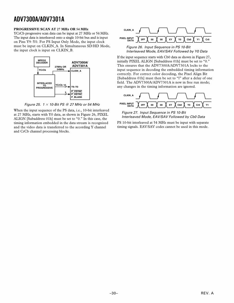
ADV7300A/ADV7301APROGRESSIVE SCAN AT 27 MHz OR 54 MHzYCrCb progressive scan data can be input at 27 MHz or 54 MHz.The input data is interleaved onto a single 10-bit bus and is inputon Pins Y9–Y0. For PS Input Only Mode, the input clockmust be input on CLKIN_A. In Simultaneous SD/HD Mode,the input clock is input on CLKIN_B.
MPEG2DECODER
P_VSYNCP_HSYNCP_BLANK
CLKIN_A
Y9–Y0
INTERLACEDTO
PROGRESSIVE
YCrCb
10
3
ADV7300A/ADV7301A27MHz OR
54MHz
YCrCb
Figure 25. 1 10-Bit PS @ 27 MHz or 54 MHz
When the input sequence of the PS data, i.e., 10-bit interleavedat 27 MHz, starts with Y0 data, as shown in Figure 26, PIXELALIGN [Subaddress 01h] must be set to “0.” In this case, thetiming information embedded in the data stream is recognizedand the video data is transferred to the according Y channeland CrCb channel processing blocks.
PIXEL INPUTDATA 3FF 00 00 XY Y0 Cb0 Y1 Cr0
CLKIN_A
Figure 26. Input Sequence in PS 10-BitInterleaved Mode, EAV/SAV Followed by Y0 Data
If the input sequence starts with Cb0 data as shown in Figure 27,initially PIXEL ALIGN [Subaddress 01h] must be set to “0.”This ensures that the ADV7300A/ADV7301A locks to theinput sequence in decoding the embedded timing informationcorrectly. For correct color decoding, the Pixel Align Bit[Subaddress 01h] must then be set to “l” after a delay of onefield. The ADV7300A/ADV7301A is now in free run mode;any changes in the timing information are ignored.
PIXEL INPUTDATA 3FF 00 00 XY Cb0 Y0 Cr0 Y1
CLKIN_A
Figure 27. Input Sequence in PS 10-BitInterleaved Mode, EAV/SAV Followed by Cb0 Data
PS 10-bit interleaved at 54 MHz must be input with separatetiming signals. EAV/SAV codes cannot be used in this mode.
REV. A
ADV7300A/ADV7301A
–31–
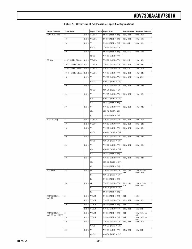
Table X. Overview of All Possible Input Configurations
Input Format Total Bits Input Video Input Pins Subaddress Register Setting
ITU-R.BT656 8 4:2:2 YCrCb S9–S2 [MSB = S9] 01h, 48h 00h, 00h
10 4:2:2 YCrCb S9–S0 [MSB = S9] 01h, 48h 00h, 10h
Y S9–S2 [MSB = S9]
CrCb Y9–Y2 [MSB = Y9]
Y S9–S0 [MSB = S9]
CrCb Y9–Y0 [MSB = Y9]
PS Only 8 (27 MHz Clock) 4:2:2 YCrCb Y9–Y2 [MSB = Y9] 01h, 13h 10h, 40h
10 (27 MHz Clock) 4:2:2 YCrCb Y9–Y0 [MSB = Y9] 01h, 13h 10h, 44h
8 (54 MHz Clock) 4:2:2 YCrCb Y9–Y2 [MSB = Y9] 01h, 13h 70h, 40h
10 (54 MHz Clock) 4:2:2 YCrCb Y9–Y0 [MSB = Y9] 01h, 13h 10h, 44h
Y Y9–Y2 [MSB = Y9]
CrCb C9–C2 [MSB = C9]
Y Y9–Y0 [MSB = Y9]
CrCb C9–C0 [MSB = C9]
Y Y9–Y2 [MSB = Y9]
Cb C9–C2 [MSB = C9]
Cr S9–S2 [MSB = S9]
Y Y9–Y0 [MSB = Y9]
Cb C9–C0 [MSB= C9]
Cr S9–S0 [MSB = S9]
HDTV Only 8 4:2:2 YCrCb Y9–Y2 [MSB = Y9] 01h, 13h 20h, 40h
10 4:2:2 YCrCb Y9–Y0 [MSB = Y9] 01h, 13h 20h, 44h
Y Y9–Y2 [MSB = Y9]
CrCb C9–Y2 [MSB = C9]
Y Y9–Y0 [MSB = Y9]
CrCb C9–C0 [MSB = C9]
Y Y9–Y2 [MSB = Y9]
Cb C9–Y2 [MSB = C9]
Cr S9–S2 [MSB = S9]
Y Y9–Y0 [MSB = Y9]
Cb C9–C0 [MSB = C9]
Cr S9–S0 [MSB = S9]
HD RGB G Y9–Y2 [MSB = Y9]
B C9–C2 [MSB = C9]
R S9–S2 [MSB = S9]
G Y9–Y0 [MSB = Y9]
B C9–C0 [MSB = C9]
R S9–S0 [MSB = S9]
ITU-R.BT656 and PS
4:2:2 YCrCb S9–S2 [MSB = S9] 01h 40h
4:2:2 YCrCb Y9–Y2 [MSB = Y9] 13h, 48h 40h, 00h
4:2:2 YCrCb S9–S0 [MSB = S9] 01h 40h
4:2:2 YCrCb Y9–Y0 [MSB = Y9] 13h, 48h 44h, 10h
ITU-R.BT656 and PS or HDTV
8 4:2:2 YCrCb S9–S2 [MSB = S9] 01h 30h, 50h, or 60h
10 4:2:2 YCrCb S9–S0 [MSB = S9] 01h 30h, 50h, or 60h
16 4:2:2 Y Y9–Y2 [MSB = Y9] 13h, 48h 40h, 00h
CrCb C9–C2 [MSB = C9]
20 4:2:2 Y Y9–Y0 [MSB = Y9] 13h, 48h 44h, 10h
CrCb C9–C0 [MSB = C9]
8
10
01h, 13h, 15h
10h or 20h, 00h, 02h
01h, 13h, 15h
10h or 20h, 04h, 02h
01h, 13h 20h, 00h
01h, 13h 20h, 04h
01h, 13h 20h, 40h
01h, 13h 20h, 44h
01h, 13h 10h, 00h
01h, 13h 10h, 04h
01h, 13h 10h, 40h
01h, 13h 10h, 44h
01h, 48h 00h, 18h
01h, 48h 00h, 08h
30 4:4:4
24
30 4:4:4
4:4:4
16
24 4:4:4
4:2:220
4:2:2
20 4:2:2
4:2:216
24
30 4:4:4
4:4:4
4:2:2
4:2:216
20
REV. A–32–
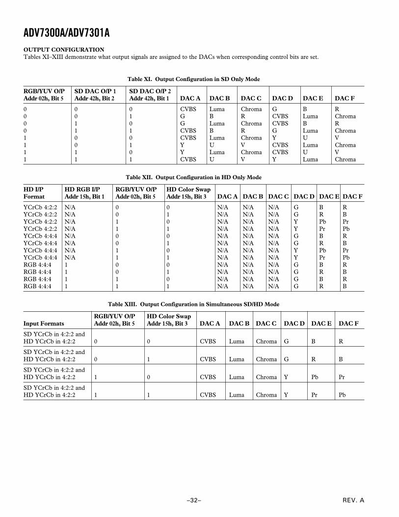
ADV7300A/ADV7301AOUTPUT CONFIGURATIONTables XI–XIII demonstrate what output signals are assigned to the DACs when corresponding control bits are set.
Table XI. Output Configuration in SD Only Mode
RGB/YUV O/P SD DAC O/P 1 SD DAC O/P 2Addr 02h, Bit 5 Addr 42h, Bit 2 Addr 42h, Bit 1 DAC A DAC B DAC C DAC D DAC E DAC F
0 0 0 CVBS Luma Chroma G B R0 0 1 G B R CVBS Luma Chroma0 1 0 G Luma Chroma CVBS B R0 1 1 CVBS B R G Luma Chroma1 0 0 CVBS Luma Chroma Y U V1 0 1 Y U V CVBS Luma Chroma1 1 0 Y Luma Chroma CVBS U V1 1 1 CVBS U V Y Luma Chroma
Table XII. Output Configuration in HD Only Mode
HD I/P HD RGB I/P RGB/YUV O/P HD Color SwapFormat Addr 15h, Bit 1 Addr 02h, Bit 5 Addr 15h, Bit 3 DAC A DAC B DAC C DAC D DAC E DAC F
YCrCb 4:2:2 N/A 0 0 N/A N/A N/A G B RYCrCb 4:2:2 N/A 0 1 N/A N/A N/A G R BYCrCb 4:2:2 N/A 1 0 N/A N/A N/A Y Pb PrYCrCb 4:2:2 N/A 1 1 N/A N/A N/A Y Pr PbYCrCb 4:4:4 N/A 0 0 N/A N/A N/A G B RYCrCb 4:4:4 N/A 0 1 N/A N/A N/A G R BYCrCb 4:4:4 N/A 1 0 N/A N/A N/A Y Pb PrYCrCb 4:4:4 N/A 1 1 N/A N/A N/A Y Pr PbRGB 4:4:4 1 0 0 N/A N/A N/A G B RRGB 4:4:4 1 0 1 N/A N/A N/A G R BRGB 4:4:4 1 1 0 N/A N/A N/A G B RRGB 4:4:4 1 1 1 N/A N/A N/A G R B
Table XIII. Output Configuration in Simultaneous SD/HD Mode
RGB/YUV O/P HD Color SwapInput Formats Addr 02h, Bit 5 Addr 15h, Bit 3 DAC A DAC B DAC C DAC D DAC E DAC F
SD YCrCb in 4:2:2 andHD YCrCb in 4:2:2 0 0 CVBS Luma Chroma G B R
SD YCrCb in 4:2:2 andHD YCrCb in 4:2:2 0 1 CVBS Luma Chroma G R B
SD YCrCb in 4:2:2 andHD YCrCb in 4:2:2 1 0 CVBS Luma Chroma Y Pb Pr
SD YCrCb in 4:2:2 andHD YCrCb in 4:2:2 1 1 CVBS Luma Chroma Y Pr Pb
REV. A
ADV7300A/ADV7301A
–33–
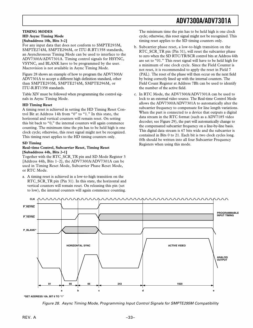
TIMING MODESHD Async Timing Mode[Subaddress 10h, Bits 3–2]For any input data that does not conform to SMPTE293M,SMPTE274M, SMPTE296M, or ITU-R.BT1358 standards,an Asynchronous Timing Mode can be used to interface to theADV7300A/ADV7301A. Timing control signals for HSYNC,VSYNC, and BLANK have to be programmed by the user.Macrovision is not available in Async Timing Mode.
Figure 28 shows an example of how to program the ADV7300A/ADV7301A to accept a different high definition standard, otherthan SMPTE293M, SMPTE274M, SMPTE296M, orITU-R.BT1358 standards.
Table XIV must be followed when programming the control sig-nals in Async Timing Mode.
HD Timing ResetA timing reset is achieved in setting the HD Timing Reset Con-trol Bit at Address 14h from “0” to “1.” In this state, thehorizontal and vertical counters will remain reset. On settingthis bit back to “0,” the internal counters will again commencecounting. The minimum time the pin has to be held high is oneclock cycle; otherwise, this reset signal might not be recognized.This timing reset applies to the HD timing counters only.
SD TimingReal-time Control, Subcarrier Reset, Timing Reset[Subaddress 44h, Bits 2–1]Together with the RTC_SCR_TR pin and SD Mode Register 3[Address 44h, Bits 1–2], the ADV7300A/ADV7301A can beused in Timing Reset Mode, Subcarrier Phase Reset Mode,or RTC Mode.
a. A timing reset is achieved in a low-to-high transition on theRTC_SCR_TR pin (Pin 31). In this state, the horizontal andvertical counters will remain reset. On releasing this pin (setto low), the internal counters will again commence counting.
The minimum time the pin has to be held high is one clockcycle; otherwise, this reset signal might not be recognized. Thistiming reset applies to the SD timing counters only.
b. Subcarrier phase reset, a low-to-high transition on theRTC_SCR_TR pin (Pin 31), will reset the subcarrier phaseto zero when the SD RTC/TR/SCR control bits at Address 44hare set to “01.” This reset signal will have to be held high fora minimum of one clock cycle. Since the Field Counter isnot reset, it is recommended to apply the reset in Field 7(PAL). The reset of the phase will then occur on the next fieldby being correctly lined up with the internal counters. TheField Count Register at Address 7Bh can be used to identifythe number of the active field.
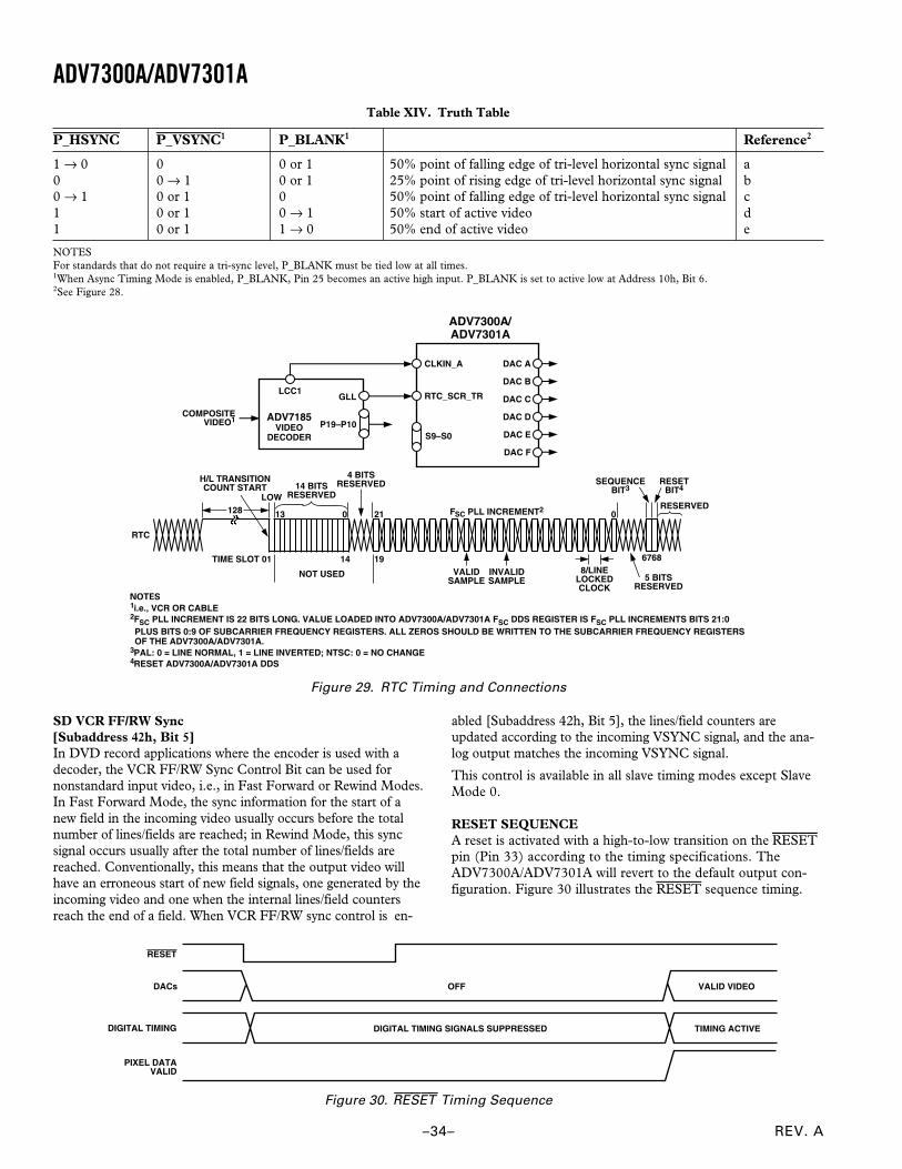
c. In RTC Mode, the ADV7300A/ADV7301A can be used tolock to an external video source. The Real-time Control Modeallows the ADV7300A/ADV7301A to automatically alter thesubcarrier frequency to compensate for line length variations.When the part is connected to a device that outputs a digitaldata stream in the RTC format (such as a ADV7185 videodecoder; see Figure 29), the part will automatically change tothe compensated subcarrier frequency on a line-by-line basis.This digital data stream is 67 bits wide and the subcarrier iscontained in Bits 0 to 21. Each bit is two clock cycles long.00h should be written into all four Subcarrier FrequencyRegisters when using this mode.
CLK
ACTIVE VIDEO
PROGRAMMABLEINPUT TIMING
ANALOGOUTPUT
a b c d
81 66 66 243 1920
HORIZONTAL SYNC
e
P_HSYNC
P_VSYNC
P_BLANK*
*SET ADDRESS 10h, BIT 6 TO “1”
Figure 28. Async Timing Mode, Programming Input Control Signals for SMPTE295M Compatibility
REV. A–34–
ADV7300A/ADV7301ATable XIV. Truth Table
P_HSYNC P_VSYNC1 P_BLANK1 Reference2
1 → 0 0 0 or 1 50% point of falling edge of tri-level horizontal sync signal a0 0 → 1 0 or 1 25% point of rising edge of tri-level horizontal sync signal b0 → 1 0 or 1 0 50% point of falling edge of tri-level horizontal sync signal c1 0 or 1 0 → 1 50% start of active video d1 0 or 1 1 → 0 50% end of active video e
NOTESFor standards that do not require a tri-sync level, P_BLANK must be tied low at all times.1When Async Timing Mode is enabled, P_BLANK, Pin 25 becomes an active high input. P_BLANK is set to active low at Address 10h, Bit 6.2See Figure 28.
LCC1GLL
P19–P10ADV7185
VIDEODECODER
COMPOSITEVIDEO1
CLKIN_A
RTC_SCR_TR
DAC A
DAC B
DAC C
DAC D
DAC E
DAC F
S9–S0
RTC
LOW
H/L TRANSITIONCOUNT START
128
TIME SLOT 01
13 0
14 BITSRESERVED
14
21
19
FSC PLL INCREMENT2
VALIDSAMPLE
INVALIDSAMPLE
8/LINELOCKEDCLOCK
6768
4 BITSRESERVED
0
SEQUENCEBIT3
RESETBIT4
RESERVED
5 BITSRESERVED
ADV7300A/ADV7301A
NOTES1i.e., VCR OR CABLE2FSC PLL INCREMENT IS 22 BITS LONG. VALUE LOADED INTO ADV7300A/ADV7301A FSC DDS REGISTER IS FSC PLL INCREMENTS BITS 21:0 PLUS BITS 0:9 OF SUBCARRIER FREQUENCY REGISTERS. ALL ZEROS SHOULD BE WRITTEN TO THE SUBCARRIER FREQUENCY REGISTERS OF THE ADV7300A/ADV7301A.
3PAL: 0 = LINE NORMAL, 1 = LINE INVERTED; NTSC: 0 = NO CHANGE4RESET ADV7300A/ADV7301A DDS
NOT USED
Figure 29. RTC Timing and Connections
SD VCR FF/RW Sync[Subaddress 42h, Bit 5]In DVD record applications where the encoder is used with adecoder, the VCR FF/RW Sync Control Bit can be used fornonstandard input video, i.e., in Fast Forward or Rewind Modes.In Fast Forward Mode, the sync information for the start of anew field in the incoming video usually occurs before the totalnumber of lines/fields are reached; in Rewind Mode, this syncsignal occurs usually after the total number of lines/fields arereached. Conventionally, this means that the output video willhave an erroneous start of new field signals, one generated by theincoming video and one when the internal lines/field countersreach the end of a field. When VCR FF/RW sync control is en-
abled [Subaddress 42h, Bit 5], the lines/field counters areupdated according to the incoming VSYNC signal, and the ana-log output matches the incoming VSYNC signal.
This control is available in all slave timing modes except SlaveMode 0.
RESET SEQUENCEA reset is activated with a high-to-low transition on the RESETpin (Pin 33) according to the timing specifications. TheADV7300A/ADV7301A will revert to the default output con-figuration. Figure 30 illustrates the RESET sequence timing.
RESET
DIGITAL TIMING
OFF
DIGITAL TIMING SIGNALS SUPPRESSED
VALID VIDEO
TIMING ACTIVE
DACs
PIXEL DATAVALID
Figure 30. RESET Timing Sequence
REV. A
ADV7300A/ADV7301A
–35–
VERTICAL BLANKING INTERVALThe ADV7300A/ADV7301A accepts input data that containsVBI data [CGMS, WSS, VITS, etc.] in SD and HD Modes.
For SMPTE293M (525 p) standards, VBI data can be inserted onLines 13 to 42 of each frame, or Lines 6 to 43 for ITU-R.BT1358(625 p) standard.
For SD NTSC, this data can be present on Lines 10 to 20, inPAL on Lines 7 to 22.
If VBI is disabled [Address 11h, Bit 4 for HD; Address 43h,Bit 4 for SD], VBI data is not present at the output and theentire VBI is blanked. These control bits are valid in all masterand slave modes.
In Slave Mode 0, if VBI is enabled, the Blanking Bit in theEAV/SAV code is overwritten and it is possible to use VBI inthis timing mode as well.
In Slave Mode 1 or 2, the BLANK Control Bit must be set toenabled [Address 4Ah, Bit 3] to allow VBI data to pass throughthe ADV7300A/ADV7301A. Otherwise, the ADV7300A/ADV7301A automatically blanks the VBI to standard.
If CGMS is enabled and VBI disabled, the CGMS data willnevertheless be available at the output.
SD SUBCARRIER FREQUENCY REGISTERS[Subaddress 4Ch–4Fh]Four 8-bit wide registers are used to set up the subcarrier fre-quency. The value of these registers is calculated in using theequation:
Subcarrier Frequency Register =
##
of Subcarrier Frequency Cycles in One Video Lineof MHz Clock Cycles in One Video Line27
232×
Example:NTSC Mode
Subcarrier Frequency =227 51716
2 56940854232.*× =
Subcarrier Register Value = 21F07C1Eh
SD FSC Register 0: 1EhSD FSC Register 1: 7ChSD FSC Register 2: F0hSD FSC Register 3: 21h
Refer to the MPU Port Description section for more detail onhow to access the subcarrier frequency registers.
SUBCARRIER PHASE REGISTER[Subaddress 50h, 5Ch, Bits 7, 6]Ten bits are used to set up the subcarrier phase. Each bit repre-sents 0.352°. For normal operation, this register is set to 00h.
FILTERSTable XV shows an overview of the programmable filters avail-able on the ADV7300A/ADV7301A.
Table XV. Selectable Filters
Filter Subaddress
SD Luma LPF NTSC 40hSD Luma LPF PAL 40hSD Luma Notch NTSC 40hSD Luma Notch PAL 40hSD Luma SSAF 40hSD Luma CIF 40hSD Luma QCIF 40hSD Chroma 0.65 MHz 40hSD Chroma 1.0 MHz 40hSD Chroma 1.3 MHz 40hSD Chroma 2.0 MHz 40hSD Chroma 3.0 MHz 40hSD Chroma CIF 40hSD Chroma QCIF 40hSD UV SSAF 42hHD Chroma Input 13hHD Sync Filter 13hHD Chroma SSAF 13h
HD Sync Filter
FREQUENCY – MHz
0.5
–0.50 305
GA
IN –
dB
10 15 20 25
0.4
0.1
–0.2
–0.3
–0.4
0.3
0.2
0
–0.1
Figure 31. HD Sync Filter Enabled
FREQUENCY – MHz
0.5
–0.50 305
GA
IN –
dB
10 15 20 25
0.4
0.1
–0.2
–0.3
–0.4
0.3
0.2
0
–0.1
Figure 32. HD Sync Filter Disabled*Rounded to the nearest integer
REV. A–36–
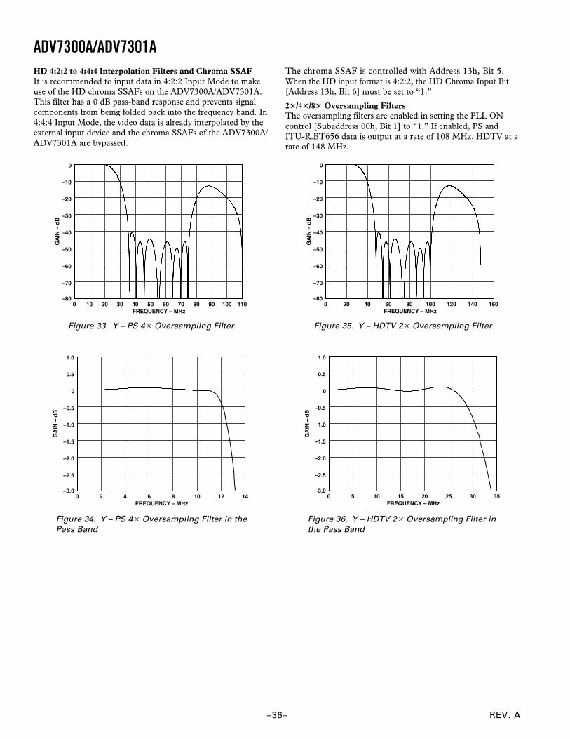
ADV7300A/ADV7301AHD 4:2:2 to 4:4:4 Interpolation Filters and Chroma SSAFIt is recommended to input data in 4:2:2 Input Mode to makeuse of the HD chroma SSAFs on the ADV7300A/ADV7301A.This filter has a 0 dB pass-band response and prevents signalcomponents from being folded back into the frequency band. In4:4:4 Input Mode, the video data is already interpolated by theexternal input device and the chroma SSAFs of the ADV7300A/ADV7301A are bypassed.
The chroma SSAF is controlled with Address 13h, Bit 5.When the HD input format is 4:2:2, the HD Chroma Input Bit[Address 13h, Bit 6] must be set to “1.”
2/4/8 Oversampling FiltersThe oversampling filters are enabled in setting the PLL ONcontrol [Subaddress 00h, Bit 1] to “1.” If enabled, PS andITU-R.BT656 data is output at a rate of 108 MHz, HDTV at arate of 148 MHz.
FREQUENCY – MHz
0
–50
–800 11010
GA
IN –
dB
20 30 40 50 60 70 80 90 100
–10
–40
–60
–70
–20
–30
Figure 33. Y – PS 4 Oversampling Filter
FREQUENCY – MHz
1.0
–1.5
–3.00 2
GA
IN –
dB
4 6 8 10 12 14
0.5
–1.0
–2.0
–2.5
0
–0.5
Figure 34. Y – PS 4 Oversampling Filter in thePass Band
FREQUENCY – MHz
0
–50
–800 16020
GA
IN –
dB
40 60 80 100 120 140
–10
–40
–60
–70
–20
–30
Figure 35. Y – HDTV 2 Oversampling Filter
FREQUENCY – MHz
1.0
–1.5
–3.00 5
GA
IN –
dB
10 15 20 25 30 35
0.5
–1.0
–2.0
–2.5
0
–0.5
Figure 36. Y – HDTV 2 Oversampling Filter inthe Pass Band
REV. A
ADV7300A/ADV7301A
–37–
FREQUENCY – MHz
0
–50
–800 11010
GA
IN –
dB
20 30 40 50 60 70 80 90 100
–10
–40
–60
–70
–20
–30
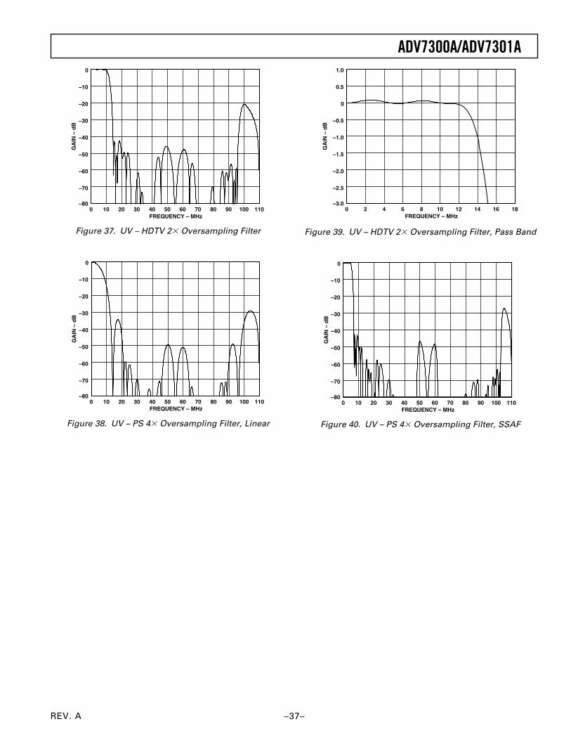
Figure 37. UV – HDTV 2 Oversampling Filter
FREQUENCY – MHz
0
–50
–800 11010
GA
IN –
dB
20 30 40 50 60 70 80 90 100
–10
–40
–60
–70
–20
–30
Figure 38. UV – PS 4 Oversampling Filter, Linear
FREQUENCY – MHz
1.0
–1.5
–3.00 182
GA
IN –
dB
4 6 8 10 12 14 16
0.5
–1.0
–2.0
–2.5
0
–0.5
Figure 39. UV – HDTV 2 Oversampling Filter, Pass Band
FREQUENCY – MHz
0
–50
–800 11010
GA
IN –
dB
20 30 40 50 60 70 80 90 100
–10
–40
–60
–70
–20
–30
Figure 40. UV – PS 4 Oversampling Filter, SSAF
REV. A–38–
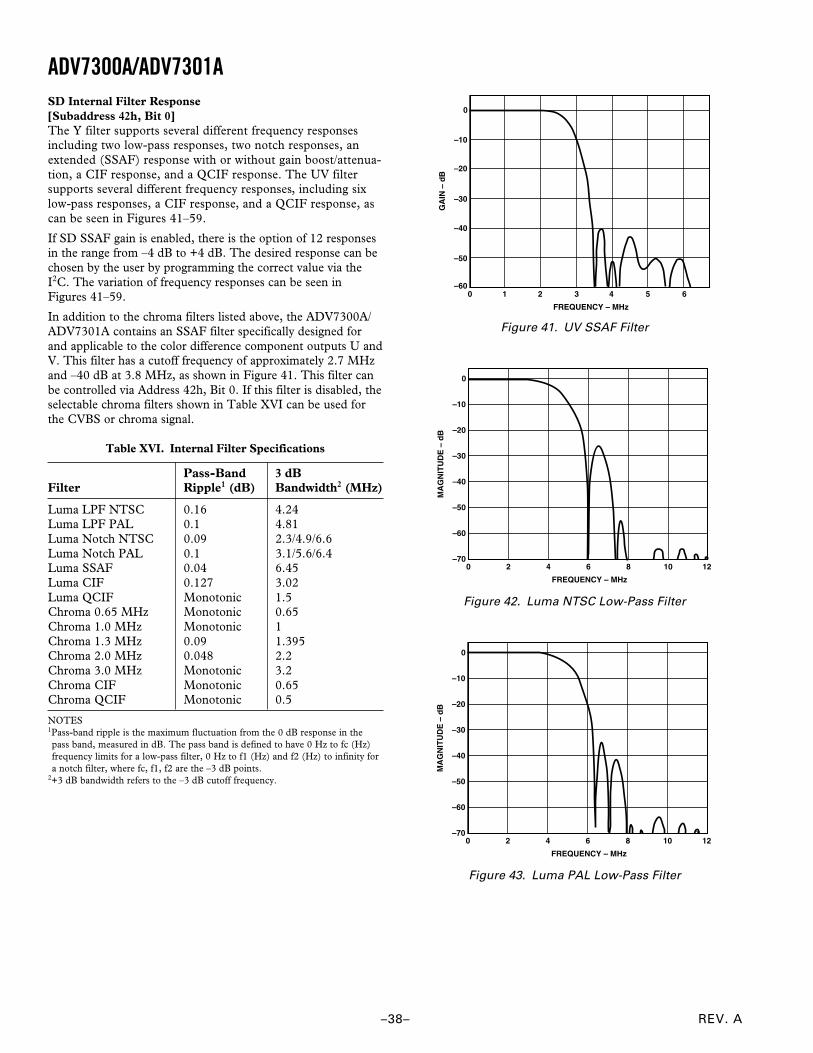
ADV7300A/ADV7301ASD Internal Filter Response[Subaddress 42h, Bit 0]The Y filter supports several different frequency responsesincluding two low-pass responses, two notch responses, anextended (SSAF) response with or without gain boost/attenua-tion, a CIF response, and a QCIF response. The UV filtersupports several different frequency responses, including sixlow-pass responses, a CIF response, and a QCIF response, ascan be seen in Figures 41–59.
If SD SSAF gain is enabled, there is the option of 12 responsesin the range from –4 dB to +4 dB. The desired response can bechosen by the user by programming the correct value via theI2C. The variation of frequency responses can be seen inFigures 41–59.
In addition to the chroma filters listed above, the ADV7300A/ADV7301A contains an SSAF filter specifically designed forand applicable to the color difference component outputs U andV. This filter has a cutoff frequency of approximately 2.7 MHzand –40 dB at 3.8 MHz, as shown in Figure 41. This filter canbe controlled via Address 42h, Bit 0. If this filter is disabled, theselectable chroma filters shown in Table XVI can be used forthe CVBS or chroma signal.
Table XVI. Internal Filter Specifications
Pass-Band 3 dBFilter Ripple1 (dB) Bandwidth2 (MHz)
Luma LPF NTSC 0.16 4.24Luma LPF PAL 0.1 4.81Luma Notch NTSC 0.09 2.3/4.9/6.6Luma Notch PAL 0.1 3.1/5.6/6.4Luma SSAF 0.04 6.45Luma CIF 0.127 3.02Luma QCIF Monotonic 1.5Chroma 0.65 MHz Monotonic 0.65Chroma 1.0 MHz Monotonic 1Chroma 1.3 MHz 0.09 1.395Chroma 2.0 MHz 0.048 2.2Chroma 3.0 MHz Monotonic 3.2Chroma CIF Monotonic 0.65Chroma QCIF Monotonic 0.5
NOTES1Pass-band ripple is the maximum fluctuation from the 0 dB response in thepass band, measured in dB. The pass band is defined to have 0 Hz to fc (Hz)frequency limits for a low-pass filter, 0 Hz to f1 (Hz) and f2 (Hz) to infinity fora notch filter, where fc, f1, f2 are the –3 dB points.
2+3 dB bandwidth refers to the –3 dB cutoff frequency.
FREQUENCY – MHz
0
0 2 3 4 5
GA
IN –
dB
–10
–30
–50
–60
–20
–40
61
Figure 41. UV SSAF Filter
FREQUENCY – MHz
0
0 2 4 6 8 12
MA
GN
ITU
DE
– d
B
–10
–30
–50
–60
–70
–20
–40
10
Figure 42. Luma NTSC Low-Pass Filter
FREQUENCY – MHz
0
0 2 4 6 8 12
MA
GN
ITU
DE
– d
B
–10
–30
–50
–60
–70
–20
–40
10
Figure 43. Luma PAL Low-Pass Filter
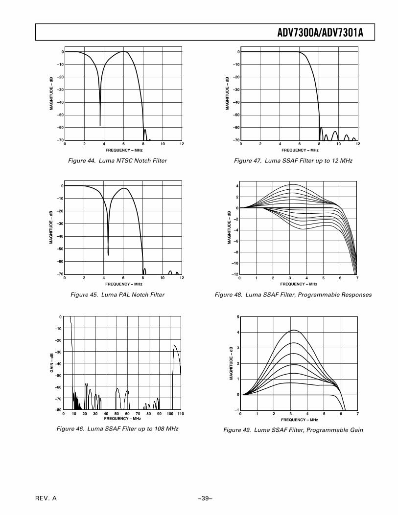
REV. A
ADV7300A/ADV7301A
–39–
FREQUENCY – MHz
0
0 2 4 6 8 12
MA
GN
ITU
DE
– d
B
–10
–30
–50
–60
–70
–20
–40
10
Figure 44. Luma NTSC Notch Filter
FREQUENCY – MHz
0
0 2 4 6 8 12
MA
GN
ITU
DE
– d
B
–10
–30
–50
–60
–70
–20
–40
10
Figure 45. Luma PAL Notch Filter
FREQUENCY – MHz
0
–50
–800 11010
GA
IN –
dB
20 30 40 50 60 70 80 90 100
–10
–40
–60
–70
–20
–30
Figure 46. Luma SSAF Filter up to 108 MHz
FREQUENCY – MHz
0
0 2 4 6 8 12
MA
GN
ITU
DE
– d
B
–10
–30
–50
–60
–70
–20
–40
10
Figure 47. Luma SSAF Filter up to 12 MHz
FREQUENCY – MHz
4
0 1 2 3 4 7
MA
GN
ITU
DE
– d
B
2
–2
–6
–8
–12
0
–4
5
–10
6
Figure 48. Luma SSAF Filter, Programmable Responses
FREQUENCY – MHz
0 1 2 3 4 7
MA
GN
ITU
DE
– d
B
5
4
2
1
–1
3
5
0
6
Figure 49. Luma SSAF Filter, Programmable Gain
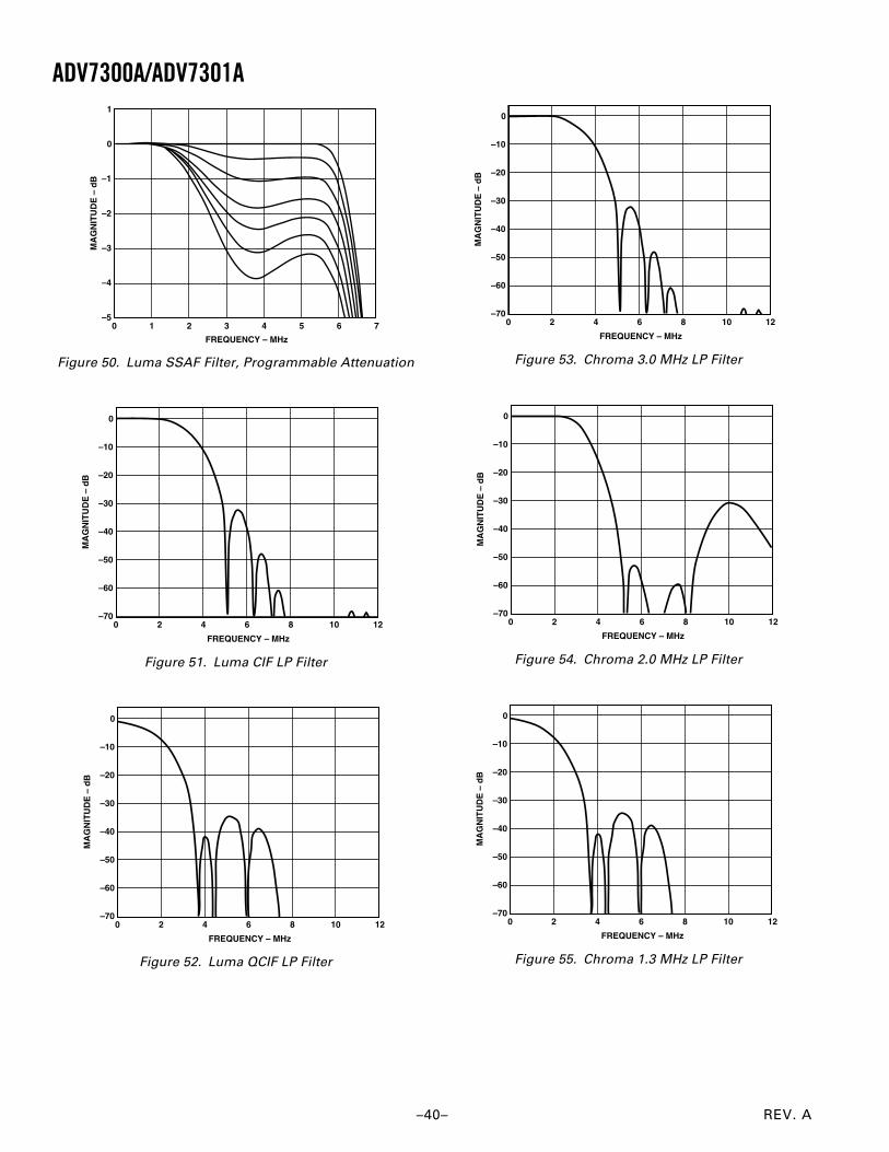
REV. A–40–
ADV7300A/ADV7301A
FREQUENCY – MHz
0 1 2 3 4 7
MA
GN
ITU
DE
– d
B
1
0
–2
–3
–5
–1
5
–4
6
Figure 50. Luma SSAF Filter, Programmable Attenuation
FREQUENCY – MHz
0
0 2 4 6 8 12
MA
GN
ITU
DE
– d
B
–10
–30
–50
–60
–70
–20
–40
10
Figure 51. Luma CIF LP Filter
FREQUENCY – MHz
0
0 2 4 6 8 12
MA
GN
ITU
DE
– d
B
–10
–30
–50
–60
–70
–20
–40
10
Figure 52. Luma QCIF LP Filter
FREQUENCY – MHz
0
0 2 4 6 8 12
MA
GN
ITU
DE
– d
B
–10
–30
–50
–60
–70
–20
–40
10
Figure 53. Chroma 3.0 MHz LP Filter
FREQUENCY – MHz
0
0 2 4 6 8 12
MA
GN
ITU
DE
– d
B
–10
–30
–50
–60
–70
–20
–40
10
Figure 54. Chroma 2.0 MHz LP Filter
FREQUENCY – MHz
0
0 2 4 6 8 12
MA
GN
ITU
DE
– d
B
–10
–30
–50
–60
–70
–20
–40
10
Figure 55. Chroma 1.3 MHz LP Filter
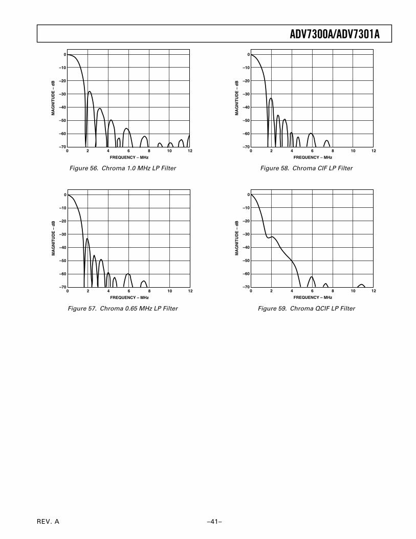
REV. A
ADV7300A/ADV7301A
–41–
FREQUENCY – MHz
0
0 2 4 6 8 12
MA
GN
ITU
DE
– d
B
–10
–30
–50
–60
–70
–20
–40
10
Figure 56. Chroma 1.0 MHz LP Filter
FREQUENCY – MHz
0
0 2 4 6 8 12
MA
GN
ITU
DE
– d
B
–10
–30
–50
–60
–70
–20
–40
10
Figure 57. Chroma 0.65 MHz LP Filter
FREQUENCY – MHz
0
0 2 4 6 8 12
MA
GN
ITU
DE
– d
B
–10
–30
–50
–60
–70
–20
–40
10
Figure 58. Chroma CIF LP Filter
FREQUENCY – MHz
0
0 2 4 6 8 12
MA
GN
ITU
DE
– d
B
–10
–30
–50
–60
–70
–20
–40
10
Figure 59. Chroma QCIF LP Filter
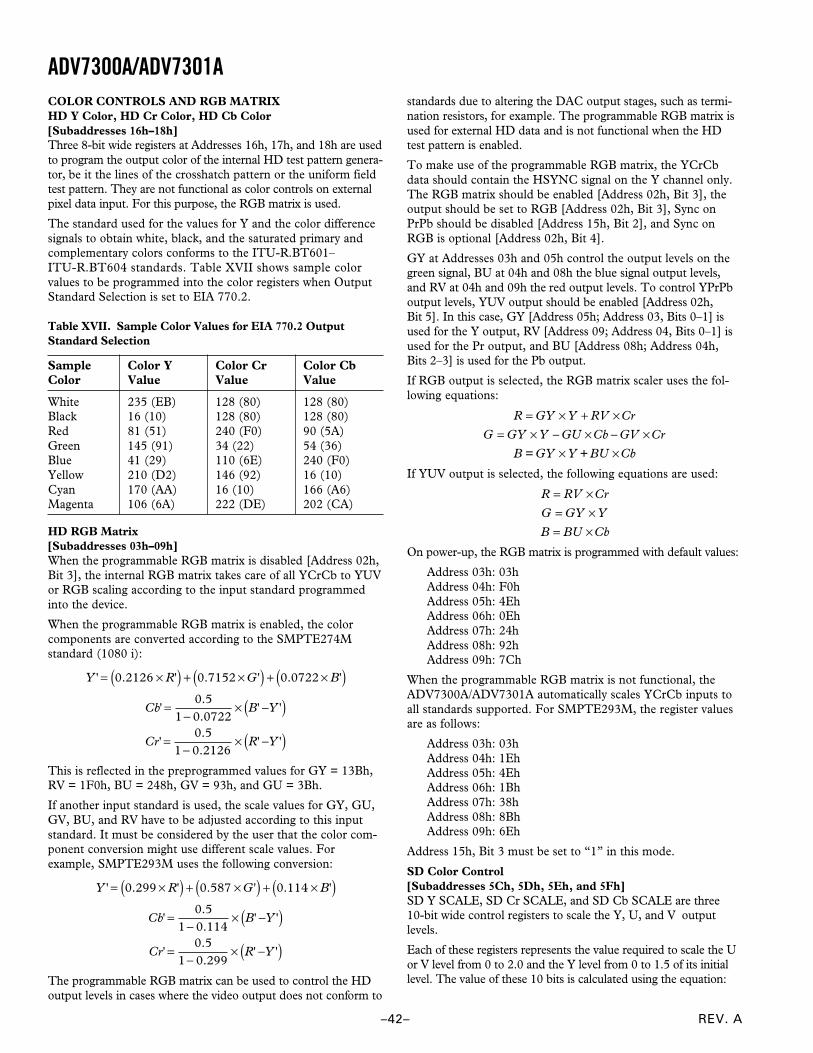
REV. A–42–
ADV7300A/ADV7301ACOLOR CONTROLS AND RGB MATRIXHD Y Color, HD Cr Color, HD Cb Color[Subaddresses 16h–18h]Three 8-bit wide registers at Addresses 16h, 17h, and 18h are usedto program the output color of the internal HD test pattern genera-tor, be it the lines of the crosshatch pattern or the uniform fieldtest pattern. They are not functional as color controls on externalpixel data input. For this purpose, the RGB matrix is used.
The standard used for the values for Y and the color differencesignals to obtain white, black, and the saturated primary andcomplementary colors conforms to the ITU-R.BT601–ITU-R.BT604 standards. Table XVII shows sample colorvalues to be programmed into the color registers when OutputStandard Selection is set to EIA 770.2.
Table XVII. Sample Color Values for EIA 770.2 OutputStandard Selection
Sample Color Y Color Cr Color CbColor Value Value Value
White 235 (EB) 128 (80) 128 (80)Black 16 (10) 128 (80) 128 (80)Red 81 (51) 240 (F0) 90 (5A)Green 145 (91) 34 (22) 54 (36)Blue 41 (29) 110 (6E) 240 (F0)Yellow 210 (D2) 146 (92) 16 (10)Cyan 170 (AA) 16 (10) 166 (A6)Magenta 106 (6A) 222 (DE) 202 (CA)
HD RGB Matrix[Subaddresses 03h–09h]When the programmable RGB matrix is disabled [Address 02h,Bit 3], the internal RGB matrix takes care of all YCrCb to YUVor RGB scaling according to the input standard programmedinto the device.
When the programmable RGB matrix is enabled, the colorcomponents are converted according to the SMPTE274Mstandard (1080 i):
Y R G B
Cb B Y
R Y
' . ' . ' . '
'..
' '
'..
' '
= ×( ) + ×( ) + ×( )=
−× −( )
=−
× −( )
0 2126 0 7152 0 0722
0 51 0 0722
0 51 0 2126
Cr
This is reflected in the preprogrammed values for GY = 13Bh,RV = 1F0h, BU = 248h, GV = 93h, and GU = 3Bh.
If another input standard is used, the scale values for GY, GU,GV, BU, and RV have to be adjusted according to this inputstandard. It must be considered by the user that the color com-ponent conversion might use different scale values. Forexample, SMPTE293M uses the following conversion:
Y R G B
Cb B Y
R Y
' . ' . ' . '
'..
' '
'..
' '
= ×( ) + ×( ) + ×( )=
−× −( )
=−
× −( )
0 299 0 587 0 114
0 51 0 114
0 51 0 299
Cr
The programmable RGB matrix can be used to control the HDoutput levels in cases where the video output does not conform to
standards due to altering the DAC output stages, such as termi-nation resistors, for example. The programmable RGB matrix isused for external HD data and is not functional when the HDtest pattern is enabled.
To make use of the programmable RGB matrix, the YCrCbdata should contain the HSYNC signal on the Y channel only.The RGB matrix should be enabled [Address 02h, Bit 3], theoutput should be set to RGB [Address 02h, Bit 3], Sync onPrPb should be disabled [Address 15h, Bit 2], and Sync onRGB is optional [Address 02h, Bit 4].
GY at Addresses 03h and 05h control the output levels on thegreen signal, BU at 04h and 08h the blue signal output levels,and RV at 04h and 09h the red output levels. To control YPrPboutput levels, YUV output should be enabled [Address 02h,Bit 5]. In this case, GY [Address 05h; Address 03, Bits 0–1] isused for the Y output, RV [Address 09; Address 04, Bits 0–1] isused for the Pr output, and BU [Address 08h; Address 04h,Bits 2–3] is used for the Pb output.
If RGB output is selected, the RGB matrix scaler uses the fol-lowing equations:
R GY Y RV
G GY Y GU Cb GV
= × + ×= × − × − ×
× ×
Cr
Cr
B = GY Y + BU Cb
If YUV output is selected, the following equations are used:
R RV
G GY Y
B BU Cb
= ×= ×= ×
Cr
On power-up, the RGB matrix is programmed with default values:
Address 03h: 03hAddress 04h: F0hAddress 05h: 4EhAddress 06h: 0EhAddress 07h: 24hAddress 08h: 92hAddress 09h: 7Ch
When the programmable RGB matrix is not functional, theADV7300A/ADV7301A automatically scales YCrCb inputs toall standards supported. For SMPTE293M, the register valuesare as follows:
Address 03h: 03hAddress 04h: 1EhAddress 05h: 4EhAddress 06h: 1BhAddress 07h: 38hAddress 08h: 8BhAddress 09h: 6Eh
Address 15h, Bit 3 must be set to “1” in this mode.
SD Color Control[Subaddresses 5Ch, 5Dh, 5Eh, and 5Fh]SD Y SCALE, SD Cr SCALE, and SD Cb SCALE are three10-bit wide control registers to scale the Y, U, and V outputlevels.
Each of these registers represents the value required to scale the Uor V level from 0 to 2.0 and the Y level from 0 to 1.5 of its initiallevel. The value of these 10 bits is calculated using the equation:
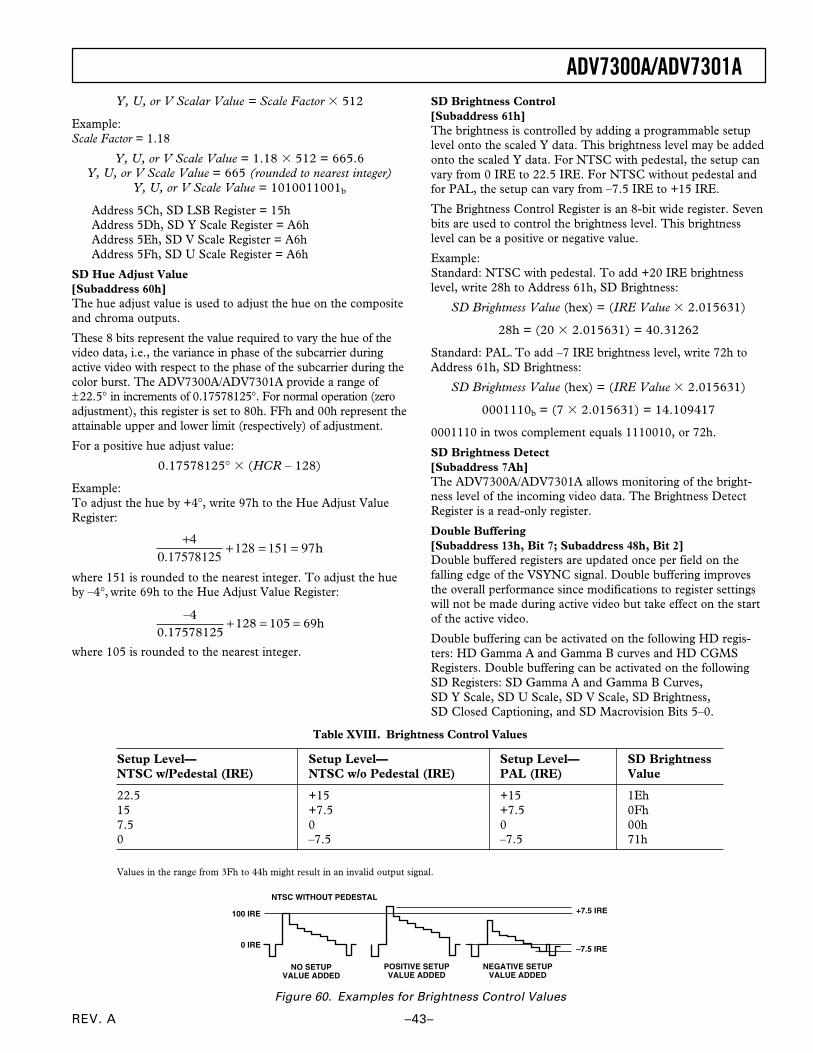
REV. A
ADV7300A/ADV7301A
–43–
Y, U, or V Scalar Value = Scale Factor 512
Example:Scale Factor = 1.18
Y, U, or V Scale Value = 1.18 512 = 665.6Y, U, or V Scale Value = 665 (rounded to nearest integer)
Y, U, or V Scale Value = 1010011001b
Address 5Ch, SD LSB Register = 15hAddress 5Dh, SD Y Scale Register = A6hAddress 5Eh, SD V Scale Register = A6hAddress 5Fh, SD U Scale Register = A6h
SD Hue Adjust Value[Subaddress 60h]The hue adjust value is used to adjust the hue on the compositeand chroma outputs.
These 8 bits represent the value required to vary the hue of thevideo data, i.e., the variance in phase of the subcarrier duringactive video with respect to the phase of the subcarrier during thecolor burst. The ADV7300A/ADV7301A provide a range of±22.5° in increments of 0.17578125°. For normal operation (zeroadjustment), this register is set to 80h. FFh and 00h represent theattainable upper and lower limit (respectively) of adjustment.
For a positive hue adjust value:
0.17578125° (HCR – 128)
Example:To adjust the hue by +4°, write 97h to the Hue Adjust ValueRegister:
++ = =
40 17578125
128 151 97.
h
where 151 is rounded to the nearest integer. To adjust the hueby –4°, write 69h to the Hue Adjust Value Register:
–.
40 17578125
128 105 69+ = = h
where 105 is rounded to the nearest integer.
SD Brightness Control[Subaddress 61h]The brightness is controlled by adding a programmable setuplevel onto the scaled Y data. This brightness level may be addedonto the scaled Y data. For NTSC with pedestal, the setup canvary from 0 IRE to 22.5 IRE. For NTSC without pedestal andfor PAL, the setup can vary from –7.5 IRE to +15 IRE.
The Brightness Control Register is an 8-bit wide register. Sevenbits are used to control the brightness level. This brightnesslevel can be a positive or negative value.
Example:Standard: NTSC with pedestal. To add +20 IRE brightnesslevel, write 28h to Address 61h, SD Brightness:
SD Brightness Value (hex) = (IRE Value 2.015631)
28h = (20 2.015631) = 40.31262
Standard: PAL. To add –7 IRE brightness level, write 72h toAddress 61h, SD Brightness:
SD Brightness Value (hex) = (IRE Value 2.015631)
0001110b = (7 2.015631) = 14.109417
0001110 in twos complement equals 1110010, or 72h.
SD Brightness Detect[Subaddress 7Ah]The ADV7300A/ADV7301A allows monitoring of the bright-ness level of the incoming video data. The Brightness DetectRegister is a read-only register.
Double Buffering[Subaddress 13h, Bit 7; Subaddress 48h, Bit 2]Double buffered registers are updated once per field on thefalling edge of the VSYNC signal. Double buffering improvesthe overall performance since modifications to register settingswill not be made during active video but take effect on the startof the active video.
Double buffering can be activated on the following HD regis-ters: HD Gamma A and Gamma B curves and HD CGMSRegisters. Double buffering can be activated on the followingSD Registers: SD Gamma A and Gamma B Curves,SD Y Scale, SD U Scale, SD V Scale, SD Brightness,SD Closed Captioning, and SD Macrovision Bits 5–0.
Table XVIII. Brightness Control Values
Setup Level— Setup Level— Setup Level— SD BrightnessNTSC w/Pedestal (IRE) NTSC w/o Pedestal (IRE) PAL (IRE) Value
22.5 +15 +15 1Eh15 +7.5 +7.5 0Fh7.5 0 0 00h0 –7.5 –7.5 71h
Values in the range from 3Fh to 44h might result in an invalid output signal.
NTSC WITHOUT PEDESTAL
NO SETUPVALUE ADDED
POSITIVE SETUPVALUE ADDED
100 IRE
0 IRE
NEGATIVE SETUPVALUE ADDED
–7.5 IRE
+7.5 IRE
Figure 60. Examples for Brightness Control Values
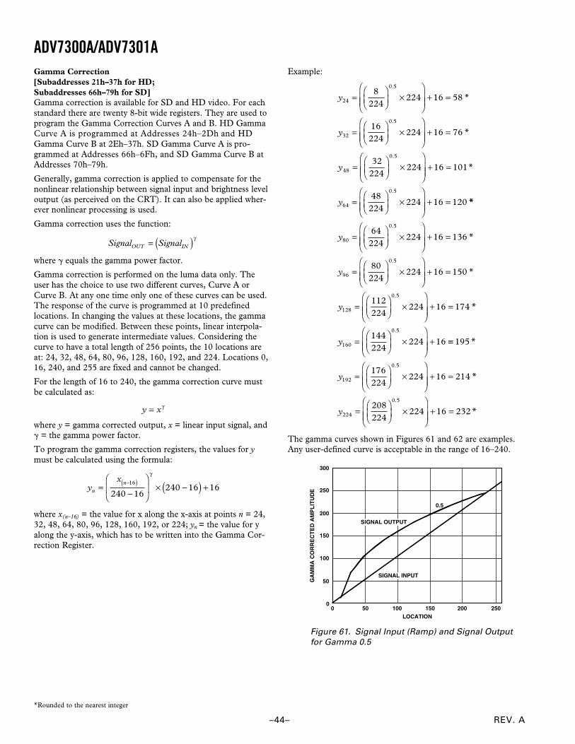
REV. A–44–
ADV7300A/ADV7301AGamma Correction[Subaddresses 21h–37h for HD;Subaddresses 66h–79h for SD]Gamma correction is available for SD and HD video. For eachstandard there are twenty 8-bit wide registers. They are used toprogram the Gamma Correction Curves A and B. HD GammaCurve A is programmed at Addresses 24h–2Dh and HDGamma Curve B at 2Eh–37h. SD Gamma Curve A is pro-grammed at Addresses 66h–6Fh, and SD Gamma Curve B atAddresses 70h–79h.
Generally, gamma correction is applied to compensate for thenonlinear relationship between signal input and brightness leveloutput (as perceived on the CRT). It can also be applied wher-ever nonlinear processing is used.
Gamma correction uses the function:
Signal SignalOUT IN= ( )γ
where equals the gamma power factor.
Gamma correction is performed on the luma data only. Theuser has the choice to use two different curves, Curve A orCurve B. At any one time only one of these curves can be used.The response of the curve is programmed at 10 predefinedlocations. In changing the values at these locations, the gammacurve can be modified. Between these points, linear interpola-tion is used to generate intermediate values. Considering thecurve to have a total length of 256 points, the 10 locations areat: 24, 32, 48, 64, 80, 96, 128, 160, 192, and 224. Locations 0,16, 240, and 255 are fixed and cannot be changed.
For the length of 16 to 240, the gamma correction curve mustbe calculated as:
y x= γ
where y = gamma corrected output, x = linear input signal, and = the gamma power factor.
To program the gamma correction registers, the values for ymust be calculated using the formula:
yx
nn
=−
× −( ) +
−( )16
240 16240 16 16
γ
where x(n–16) = the value for x along the x-axis at points n = 24,32, 48, 64, 80, 96, 128, 160, 192, or 224; yn = the value for yalong the y-axis, which has to be written into the Gamma Cor-rection Register.
Example:
y
y
y
y
24
0 5
32
0 5
48
0 5
64
0 5
8224
224 16 58
16224
224 16 76
32224
224 16 101
48224
224 16 120
=
×
+ =
=
×
+ =
=
×
+ =
=
×
+ =
.
.
.
.
*
*
*
**
*
*
*
y
y
y
y
80
0 5
96
0 5
128
0 5
160
0 5
64224
224 16 136
80224
224 16 150
112224
224 16 174
144224
224 16
=
×
+ =
=
×
+ =
=
×
+ =
=
×
+
.
.
.
.
==
=
×
+ =
=
×
+ =
195
176224
224 16 214
208224
224 16 232
192
0 5
224
0 5
*
*
*
y
y
.
.
The gamma curves shown in Figures 61 and 62 are examples.Any user-defined curve is acceptable in the range of 16–240.
LOCATION
00
50
100
150
200
250
300
50 100 150 200 250
0.5
SIGNAL INPUT
SIGNAL OUTPUT
GA
MM
A C
OR
RE
CT
ED
AM
PL
ITU
DE
Figure 61. Signal Input (Ramp) and Signal Outputfor Gamma 0.5
*Rounded to the nearest integer
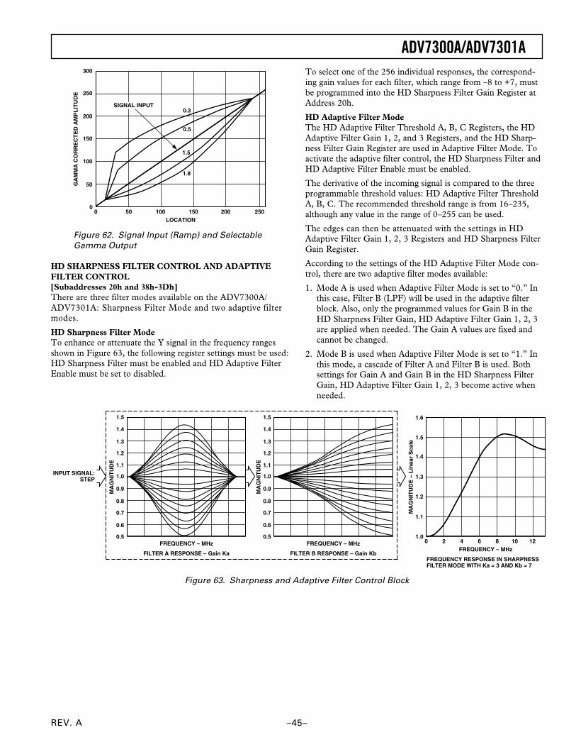
REV. A
ADV7300A/ADV7301A
–45–
LOCATION
00
50
100
150
200
250
300
50 100 150 200 250
0.3
0.5
1.5
1.8
SIGNAL INPUT
GA
MM
A C
OR
RE
CT
ED
AM
PL
ITU
DE
Figure 62. Signal Input (Ramp) and SelectableGamma Output
HD SHARPNESS FILTER CONTROL AND ADAPTIVEFILTER CONTROL[Subaddresses 20h and 38h-3Dh]There are three filter modes available on the ADV7300A/ADV7301A: Sharpness Filter Mode and two adaptive filtermodes.
HD Sharpness Filter ModeTo enhance or attenuate the Y signal in the frequency rangesshown in Figure 63, the following register settings must be used:HD Sharpness Filter must be enabled and HD Adaptive FilterEnable must be set to disabled.
To select one of the 256 individual responses, the correspond-ing gain values for each filter, which range from –8 to +7, mustbe programmed into the HD Sharpness Filter Gain Register atAddress 20h.
HD Adaptive Filter ModeThe HD Adaptive Filter Threshold A, B, C Registers, the HDAdaptive Filter Gain 1, 2, and 3 Registers, and the HD Sharp-ness Filter Gain Register are used in Adaptive Filter Mode. Toactivate the adaptive filter control, the HD Sharpness Filter andHD Adaptive Filter Enable must be enabled.
The derivative of the incoming signal is compared to the threeprogrammable threshold values: HD Adaptive Filter ThresholdA, B, C. The recommended threshold range is from 16–235,although any value in the range of 0–255 can be used.
The edges can then be attenuated with the settings in HDAdaptive Filter Gain 1, 2, 3 Registers and HD Sharpness FilterGain Register.
According to the settings of the HD Adaptive Filter Mode con-trol, there are two adaptive filter modes available:
1. Mode A is used when Adaptive Filter Mode is set to “0.” Inthis case, Filter B (LPF) will be used in the adaptive filterblock. Also, only the programmed values for Gain B in theHD Sharpness Filter Gain, HD Adaptive Filter Gain 1, 2, 3are applied when needed. The Gain A values are fixed andcannot be changed.
2. Mode B is used when Adaptive Filter Mode is set to “1.” Inthis mode, a cascade of Filter A and Filter B is used. Bothsettings for Gain A and Gain B in the HD Sharpness FilterGain, HD Adaptive Filter Gain 1, 2, 3 become active whenneeded.
FREQUENCY – MHz
MA
GN
ITU
DE
0.5
0.6
0.7
0.8
0.9
1.0
1.1
1.2
1.3
1.4
1.5
FILTER A RESPONSE – Gain Ka
FREQUENCY – MHz
MA
GN
ITU
DE
0.5
0.6
0.7
0.8
0.9
1.0
1.1
1.2
1.3
1.4
1.5
FILTER B RESPONSE – Gain KbFREQUENCY – MHz
MA
GN
ITU
DE
– L
inea
r S
cale
1.0
1.1
1.2
1.3
1.4
1.5
1.6
0 2 4 6 8 10 12
INPUT SIGNAL:STEP
FREQUENCY RESPONSE IN SHARPNESSFILTER MODE WITH Ka = 3 AND Kb = 7
Figure 63. Sharpness and Adaptive Filter Control Block
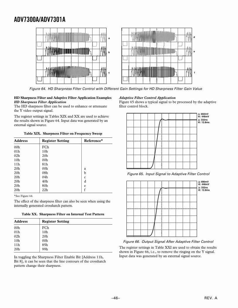
REV. A–46–
ADV7300A/ADV7301A
HD Sharpness Filter and Adaptive Filter Application ExamplesHD Sharpness Filter ApplicationThe HD sharpness filter can be used to enhance or attenuatethe Y video output signal.
The register settings in Tables XIX and XX are used to achievethe results shown in Figure 64. Input data was generated by anexternal signal source.
Table XIX. Sharpness Filter on Frequency Sweep
Address Register Setting Reference*
00h FCh01h 10h02h 20h10h 00h11h 81h20h 00h a20h 08h b20h 04h c20h 40h d20h 80h e20h 22h f
*See Figure 64.
The effect of the sharpness filter can also be seen when using theinternally generated crosshatch pattern.
Table XX. Sharpness Filter on Internal Test Pattern
Address Register Setting
00h FCh01h 10h02h 20h10h 00h11h 85h20h 99h
In toggling the Sharpness Filter Enable Bit [Address 11h,Bit 8], it can be seen that the line contours of the crosshatchpattern change their sharpness.
f
e
da
b
c
Figure 64. HD Sharpness Filter Control with Different Gain Settings for HD Sharpness Filter Gain Value
Adaptive Filter Control ApplicationFigure 65 shows a typical signal to be processed by the adaptivefilter control block.
: 692mV@: 446mV: 332ns@: 12.8ms
Figure 65. Input Signal to Adaptive Filter Control
: 690mV@: 446mV: 332ns@: 12.8ms
Figure 66. Output Signal After Adaptive Filter Control
The register settings in Table XXI are used to obtain the resultsshown in Figure 66, i.e., to remove the ringing on the Y signal.Input data was generated by an external signal source.
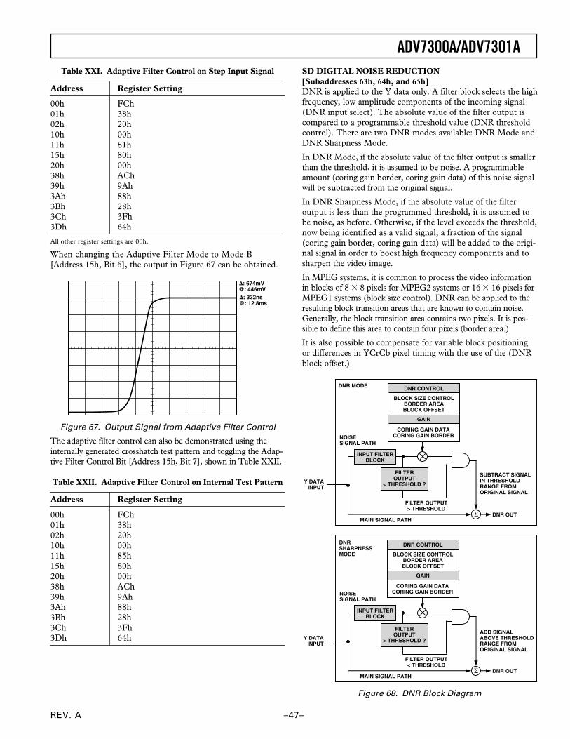
REV. A
ADV7300A/ADV7301A
–47–
Table XXI. Adaptive Filter Control on Step Input Signal
Address Register Setting
00h FCh01h 38h02h 20h10h 00h11h 81h15h 80h20h 00h38h ACh39h 9Ah3Ah 88h3Bh 28h3Ch 3Fh3Dh 64h
All other register settings are 00h.
When changing the Adaptive Filter Mode to Mode B[Address 15h, Bit 6], the output in Figure 67 can be obtained.
: 674mV@: 446mV: 332ns@: 12.8ms
Figure 67. Output Signal from Adaptive Filter Control
The adaptive filter control can also be demonstrated using theinternally generated crosshatch test pattern and toggling the Adap-tive Filter Control Bit [Address 15h, Bit 7], shown in Table XXII.
Table XXII. Adaptive Filter Control on Internal Test Pattern
Address Register Setting
00h FCh01h 38h02h 20h10h 00h11h 85h15h 80h20h 00h38h ACh39h 9Ah3Ah 88h3Bh 28h3Ch 3Fh3Dh 64h
SD DIGITAL NOISE REDUCTION[Subaddresses 63h, 64h, and 65h]DNR is applied to the Y data only. A filter block selects the highfrequency, low amplitude components of the incoming signal(DNR input select). The absolute value of the filter output iscompared to a programmable threshold value (DNR thresholdcontrol). There are two DNR modes available: DNR Mode andDNR Sharpness Mode.
In DNR Mode, if the absolute value of the filter output is smallerthan the threshold, it is assumed to be noise. A programmableamount (coring gain border, coring gain data) of this noise signalwill be subtracted from the original signal.
In DNR Sharpness Mode, if the absolute value of the filteroutput is less than the programmed threshold, it is assumed tobe noise, as before. Otherwise, if the level exceeds the threshold,now being identified as a valid signal, a fraction of the signal(coring gain border, coring gain data) will be added to the origi-nal signal in order to boost high frequency components and tosharpen the video image.
In MPEG systems, it is common to process the video informationin blocks of 8 8 pixels for MPEG2 systems or 16 16 pixels forMPEG1 systems (block size control). DNR can be applied to theresulting block transition areas that are known to contain noise.Generally, the block transition area contains two pixels. It is pos-sible to define this area to contain four pixels (border area.)
It is also possible to compensate for variable block positioningor differences in YCrCb pixel timing with the use of the (DNRblock offset.)
BLOCK SIZE CONTROLBORDER AREABLOCK OFFSET
CORING GAIN DATACORING GAIN BORDER
GAIN
DNR CONTROL
FILTEROUTPUT
> THRESHOLD ?
INPUT FILTERBLOCK
FILTER OUTPUT< THRESHOLD
DNR OUTMAIN SIGNAL PATH
ADD SIGNALABOVE THRESHOLDRANGE FROMORIGINAL SIGNAL
DNRSHARPNESSMODE
NOISESIGNAL PATH
Y DATAINPUT
BLOCK SIZE CONTROLBORDER AREABLOCK OFFSET
CORING GAIN DATACORING GAIN BORDER
GAIN
DNR CONTROL
FILTEROUTPUT
< THRESHOLD ?
INPUT FILTERBLOCK
FILTER OUTPUT> THRESHOLD
DNR OUTMAIN SIGNAL PATH
SUBTRACT SIGNALIN THRESHOLDRANGE FROMORIGINAL SIGNAL
DNR MODE
NOISESIGNAL PATH
Y DATAINPUT
Figure 68. DNR Block Diagram
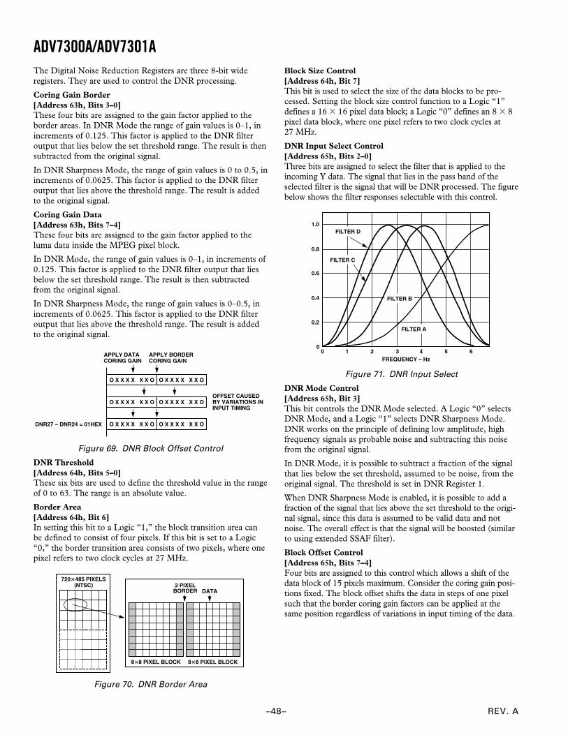
REV. A–48–
ADV7300A/ADV7301AThe Digital Noise Reduction Registers are three 8-bit wideregisters. They are used to control the DNR processing.
Coring Gain Border[Address 63h, Bits 3–0]These four bits are assigned to the gain factor applied to theborder areas. In DNR Mode the range of gain values is 0–1, inincrements of 0.125. This factor is applied to the DNR filteroutput that lies below the set threshold range. The result is thensubtracted from the original signal.
In DNR Sharpness Mode, the range of gain values is 0 to 0.5, inincrements of 0.0625. This factor is applied to the DNR filteroutput that lies above the threshold range. The result is addedto the original signal.
Coring Gain Data[Address 63h, Bits 7–4]These four bits are assigned to the gain factor applied to theluma data inside the MPEG pixel block.
In DNR Mode, the range of gain values is 0–1, in increments of0.125. This factor is applied to the DNR filter output that liesbelow the set threshold range. The result is then subtractedfrom the original signal.
In DNR Sharpness Mode, the range of gain values is 0–0.5, inincrements of 0.0625. This factor is applied to the DNR filteroutput that lies above the threshold range. The result is addedto the original signal.
O X X X X X X O O X X X X X X O
O X X X X X X O O X X X X X X O
O X X X X X X O O X X X X X X ODNR27 – DNR24 = 01HEX
OFFSET CAUSEDBY VARIATIONS ININPUT TIMING
APPLY BORDERCORING GAIN
APPLY DATACORING GAIN
Figure 69. DNR Block Offset Control
DNR Threshold[Address 64h, Bits 5–0]These six bits are used to define the threshold value in the rangeof 0 to 63. The range is an absolute value.
Border Area[Address 64h, Bit 6]In setting this bit to a Logic “1,” the block transition area canbe defined to consist of four pixels. If this bit is set to a Logic“0,” the border transition area consists of two pixels, where onepixel refers to two clock cycles at 27 MHz.
720485 PIXELS(NTSC)
88 PIXEL BLOCK 88 PIXEL BLOCK
2 PIXELBORDER DATA
Figure 70. DNR Border Area
Block Size Control[Address 64h, Bit 7]This bit is used to select the size of the data blocks to be pro-cessed. Setting the block size control function to a Logic “1”defines a 16 16 pixel data block; a Logic “0” defines an 8 8pixel data block, where one pixel refers to two clock cycles at27 MHz.
DNR Input Select Control[Address 65h, Bits 2–0]Three bits are assigned to select the filter that is applied to theincoming Y data. The signal that lies in the pass band of theselected filter is the signal that will be DNR processed. The figurebelow shows the filter responses selectable with this control.
FILTER C
FILTER B
FILTER A
FILTER D
FREQUENCY – Hz
00 1 2 3 4 5 6
0.2
0.4
0.6
0.8
1.0
Figure 71. DNR Input Select
DNR Mode Control[Address 65h, Bit 3]This bit controls the DNR Mode selected. A Logic “0” selectsDNR Mode, and a Logic “1” selects DNR Sharpness Mode.DNR works on the principle of defining low amplitude, highfrequency signals as probable noise and subtracting this noisefrom the original signal.
In DNR Mode, it is possible to subtract a fraction of the signalthat lies below the set threshold, assumed to be noise, from theoriginal signal. The threshold is set in DNR Register 1.
When DNR Sharpness Mode is enabled, it is possible to add afraction of the signal that lies above the set threshold to the origi-nal signal, since this data is assumed to be valid data and notnoise. The overall effect is that the signal will be boosted (similarto using extended SSAF filter).
Block Offset Control[Address 65h, Bits 7–4]Four bits are assigned to this control which allows a shift of thedata block of 15 pixels maximum. Consider the coring gain posi-tions fixed. The block offset shifts the data in steps of one pixelsuch that the border coring gain factors can be applied at thesame position regardless of variations in input timing of the data.
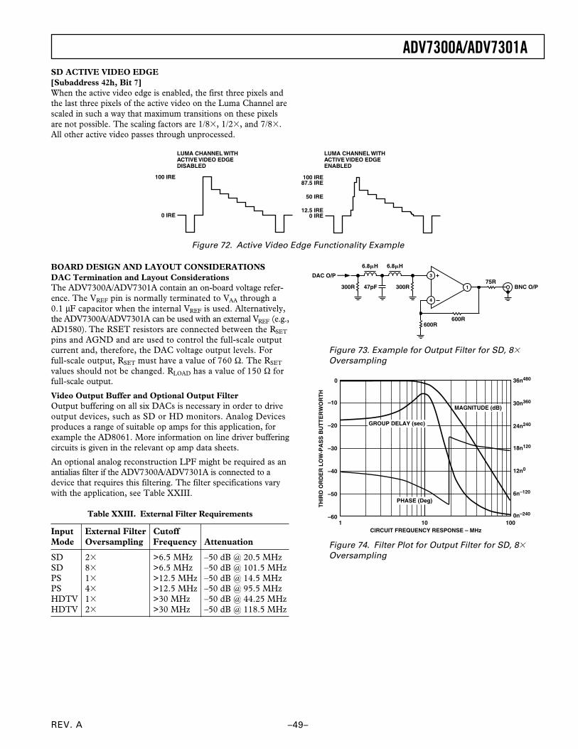
REV. A
ADV7300A/ADV7301A
–49–
SD ACTIVE VIDEO EDGE[Subaddress 42h, Bit 7]When the active video edge is enabled, the first three pixels andthe last three pixels of the active video on the Luma Channel arescaled in such a way that maximum transitions on these pixelsare not possible. The scaling factors are 1/8, 1/2, and 7/8.All other active video passes through unprocessed.
100 IRE
0 IRE
100 IRE
12.5 IRE
87.5 IRE
0 IRE
50 IRE
LUMA CHANNEL WITHACTIVE VIDEO EDGEDISABLED
LUMA CHANNEL WITHACTIVE VIDEO EDGEENABLED
Figure 72. Active Video Edge Functionality Example
BOARD DESIGN AND LAYOUT CONSIDERATIONSDAC Termination and Layout ConsiderationsThe ADV7300A/ADV7301A contain an on-board voltage refer-ence. The VREF pin is normally terminated to VAA through a0.1 µF capacitor when the internal VREF is used. Alternatively,the ADV7300A/ADV7301A can be used with an external VREF (e.g.,AD1580). The RSET resistors are connected between the RSET
pins and AGND and are used to control the full-scale outputcurrent and, therefore, the DAC voltage output levels. Forfull-scale output, RSET must have a value of 760 Ω. The RSET
values should not be changed. RLOAD has a value of 150 Ω forfull-scale output.
Video Output Buffer and Optional Output FilterOutput buffering on all six DACs is necessary in order to driveoutput devices, such as SD or HD monitors. Analog Devicesproduces a range of suitable op amps for this application, forexample the AD8061. More information on line driver bufferingcircuits is given in the relevant op amp data sheets.
An optional analog reconstruction LPF might be required as anantialias filter if the ADV7300A/ADV7301A is connected to adevice that requires this filtering. The filter specifications varywith the application, see Table XXIII.
Table XXIII. External Filter Requirements
Input External Filter CutoffMode Oversampling Frequency Attenuation
SD 2 >6.5 MHz –50 dB @ 20.5 MHzSD 8 >6.5 MHz –50 dB @ 101.5 MHzPS 1 >12.5 MHz –50 dB @ 14.5 MHzPS 4 >12.5 MHz –50 dB @ 95.5 MHzHDTV 1 >30 MHz –50 dB @ 44.25 MHzHDTV 2 >30 MHz –50 dB @ 118.5 MHz
600R600R
300R47pF300R
DAC O/P75R
BNC O/P
6.8H 6.8H
Figure 73. Example for Output Filter for SD, 8Oversampling
CIRCUIT FREQUENCY RESPONSE – MHz
–601 10 100
0n–240
6n–120
12n0
18n120
24n240
30n360
36n480
–50
–40
–30
–20
–10
0
GROUP DELAY (sec)
PHASE (Deg)
MAGNITUDE (dB)
TH
IRD
OR
DE
R L
OW
-PA
SS
BU
TT
ER
WO
RT
H
Figure 74. Filter Plot for Output Filter for SD, 8Oversampling
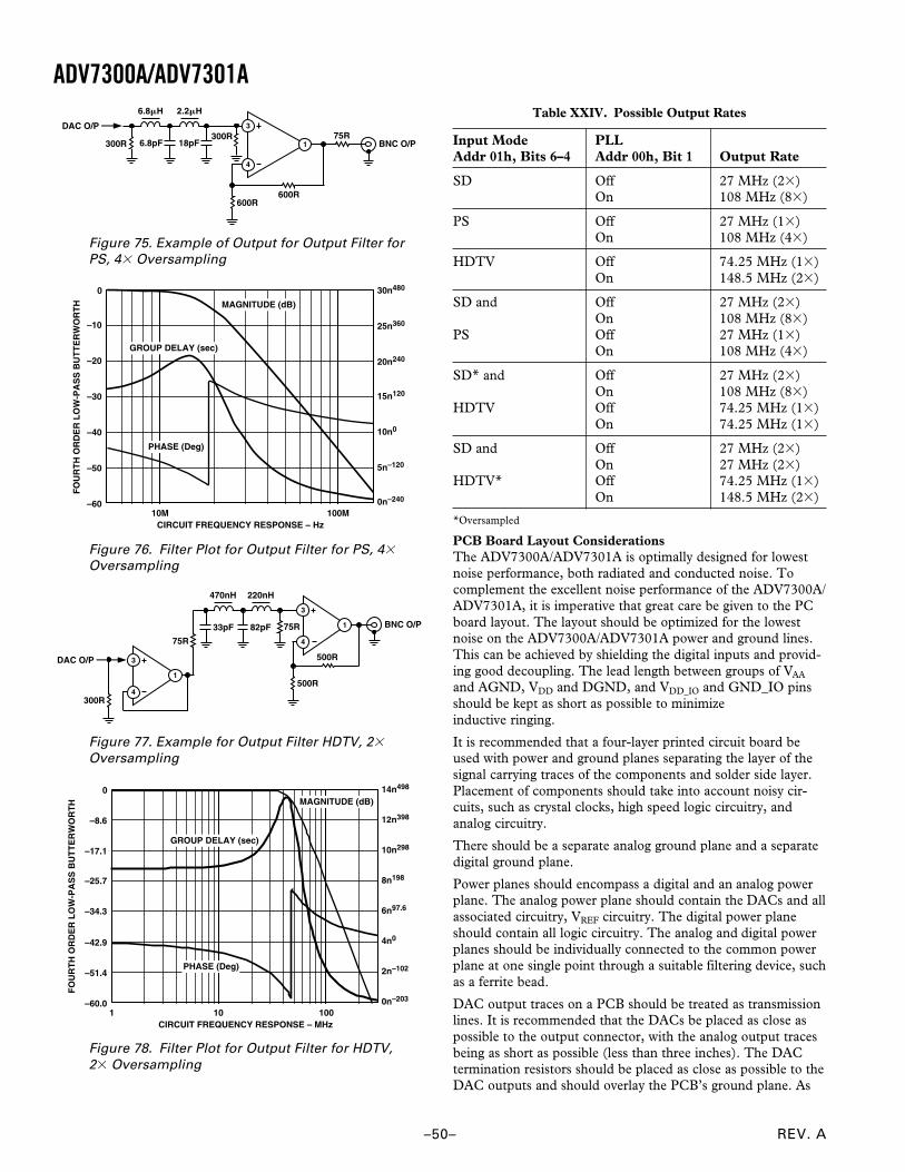
REV. A–50–
ADV7300A/ADV7301A
600R
6.8pF300R
DAC O/P75R
BNC O/P
6.8H 2.2H
18pF300R
600R
Figure 75. Example of Output for Output Filter forPS, 4 Oversampling
CIRCUIT FREQUENCY RESPONSE – Hz
–6010M
0n–240
5n–120
10n0
15n120
20n240
25n360
30n480
–50
–40
–30
–20
–10
0
GROUP DELAY (sec)
PHASE (Deg)
MAGNITUDE (dB)
100M
FO
UR
TH
OR
DE
R L
OW
-PA
SS
BU
TT
ER
WO
RT
H
Figure 76. Filter Plot for Output Filter for PS, 4Oversampling
500R
33pF
DAC O/P
75R
BNC O/P
470nH 220nH
82pF
500R
75R
300R
Figure 77. Example for Output Filter HDTV, 2Oversampling
CIRCUIT FREQUENCY RESPONSE – MHz
–60.01 10 100
0n–203
2n–102
4n0
6n97.6
8n198
10n298
12n398
–51.4
–42.9
–34.3
–25.7
–8.6
0MAGNITUDE (dB)
GROUP DELAY (sec)
PHASE (Deg)
FO
UR
TH
OR
DE
R L
OW
-PA
SS
BU
TT
ER
WO
RT
H
14n498
–17.1
Figure 78. Filter Plot for Output Filter for HDTV,2 Oversampling
Table XXIV. Possible Output Rates
Input Mode PLLAddr 01h, Bits 6–4 Addr 00h, Bit 1 Output Rate
SD Off 27 MHz (2)On 108 MHz (8)
PS Off 27 MHz (1)On 108 MHz (4)
HDTV Off 74.25 MHz (1)On 148.5 MHz (2)
SD and Off 27 MHz (2)On 108 MHz (8)
PS Off 27 MHz (1)On 108 MHz (4)
SD* and Off 27 MHz (2)On 108 MHz (8)
HDTV Off 74.25 MHz (1)On 74.25 MHz (1)
SD and Off 27 MHz (2)On 27 MHz (2)
HDTV* Off 74.25 MHz (1)On 148.5 MHz (2)
*Oversampled
PCB Board Layout ConsiderationsThe ADV7300A/ADV7301A is optimally designed for lowestnoise performance, both radiated and conducted noise. Tocomplement the excellent noise performance of the ADV7300A/ADV7301A, it is imperative that great care be given to the PCboard layout. The layout should be optimized for the lowestnoise on the ADV7300A/ADV7301A power and ground lines.This can be achieved by shielding the digital inputs and provid-ing good decoupling. The lead length between groups of VAA
and AGND, VDD and DGND, and VDD_IO and GND_IO pinsshould be kept as short as possible to minimizeinductive ringing.
It is recommended that a four-layer printed circuit board beused with power and ground planes separating the layer of thesignal carrying traces of the components and solder side layer.Placement of components should take into account noisy cir-cuits, such as crystal clocks, high speed logic circuitry, andanalog circuitry.
There should be a separate analog ground plane and a separatedigital ground plane.
Power planes should encompass a digital and an analog powerplane. The analog power plane should contain the DACs and allassociated circuitry, VREF circuitry. The digital power planeshould contain all logic circuitry. The analog and digital powerplanes should be individually connected to the common powerplane at one single point through a suitable filtering device, suchas a ferrite bead.
DAC output traces on a PCB should be treated as transmissionlines. It is recommended that the DACs be placed as close aspossible to the output connector, with the analog output tracesbeing as short as possible (less than three inches). The DACtermination resistors should be placed as close as possible to theDAC outputs and should overlay the PCB’s ground plane. As
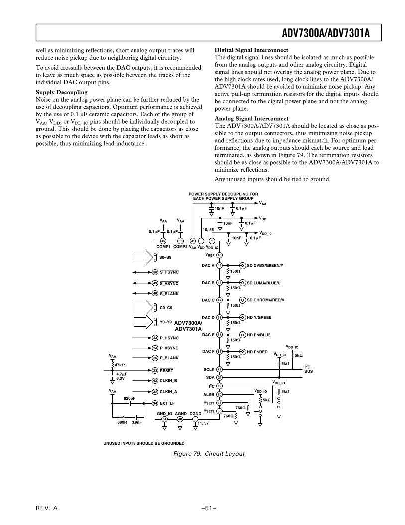
REV. A
ADV7300A/ADV7301A
–51–
well as minimizing reflections, short analog output traces willreduce noise pickup due to neighboring digital circuitry.
To avoid crosstalk between the DAC outputs, it is recommendedto leave as much space as possible between the tracks of theindividual DAC output pins.
Supply DecouplingNoise on the analog power plane can be further reduced by theuse of decoupling capacitors. Optimum performance is achievedby the use of 0.1 µF ceramic capacitors. Each of the group ofVAA, VDD, or VDD_IO pins should be individually decoupled toground. This should be done by placing the capacitors as closeas possible to the device with the capacitor leads as short aspossible, thus minimizing lead inductance.
Digital Signal InterconnectThe digital signal lines should be isolated as much as possiblefrom the analog outputs and other analog circuitry. Digitalsignal lines should not overlay the analog power plane. Due tothe high clock rates used, long clock lines to the ADV7300A/ADV7301A should be avoided to minimize noise pickup. Anyactive pull-up termination resistors for the digital inputs shouldbe connected to the digital power plane and not the analogpower plane.
Analog Signal InterconnectThe ADV7300A/ADV7301A should be located as close as pos-sible to the output connectors, thus minimizing noise pickupand reflections due to impedance mismatch. For optimum per-formance, the analog outputs should each be source and loadterminated, as shown in Figure 79. The termination resistorsshould be as close as possible to the ADV7300A/ADV7301A tominimize reflections.
Any unused inputs should be tied to ground.
S_HSYNC
S0–S9
S_VSYNC
S BLANK
C0–C9
Y0–Y9
P_HSYNC
P_VSYNC
P_BLANK
RESET
CLKIN_B
CLKIN_A
EXT_LF
GND_IO AGND DGNDRSET2
RSET1
ALSB
I2C
SCLK
DAC F
DAC E
DAC D
DAC C
DAC B
DAC A
VREF
VDD_IOVDDVAACOMP2COMP1
150
150
150
150
SDA
11, 57
760
760
5k
VDD_IO 5k
VDD_IO
5k
VDD_IOHD Pr/RED
5k
VDD_IO
HD Pb/BLUE
HD Y/GREEN
SD CHROMA/RED/V
SD LUMA/BLUE/U
SD CVBS/GREEN/Y
3.9nF680R
820pF
VAA
4.7F6.3V
150
VAA
UNUSED INPUTS SHOULD BE GROUNDED
47k
VAA VAA
0.1F 0.1F
0.1F
VAA0.1F
10nF 0.1F
10nF
10nF
10, 56VDD_IO
VDD
I2CBUS
ADV7300A/ADV7301A
POWER SUPPLY DECOUPLING FOREACH POWER SUPPLY GROUP
150
Figure 79. Circuit Layout
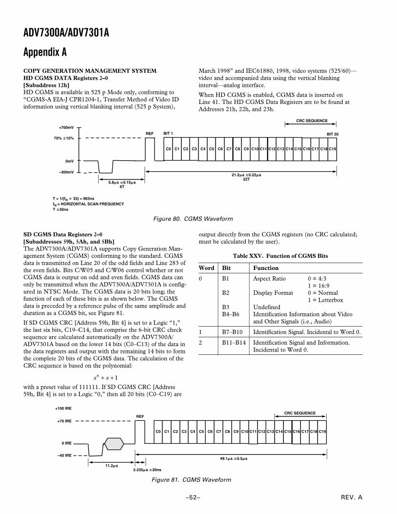
REV. A–52–
ADV7300A/ADV7301A
Appendix ACOPY GENERATION MANAGEMENT SYSTEMHD CGMS DATA Registers 2–0[Subaddress 12h]HD CGMS is available in 525 p Mode only, conforming to“CGMS-A EIA-J CPR1204-1, Transfer Method of Video IDinformation using vertical blanking interval (525 p System),
March 1998” and IEC61880, 1998, video systems (525/60)—video and accompanied data using the vertical blankinginterval—analog interface.
When HD CGMS is enabled, CGMS data is inserted onLine 41. The HD CGMS Data Registers are to be found atAddresses 21h, 22h, and 23h.
C0 C1 C2 C3 C4 C5 C6 C7 C8 C9 C10 C11 C12 C13 C14 C15 C16 C17 C18 C19
CRC SEQUENCE
21.2s 0.22s22T
REF
5.8s 0.15s6T
0mV
–300mV
70% 10%BIT 1
T = 1/(fH 33) = 963nsfH = HORIZONTAL SCAN FREQUENCYT 30ns
+700mV
BIT 20
Figure 80. CGMS Waveform
SD CGMS Data Registers 2–0[Subaddresses 59h, 5Ah, and 5Bh]The ADV7300A/ADV7301A supports Copy Generation Man-agement System (CGMS) conforming to the standard. CGMSdata is transmitted on Line 20 of the odd fields and Line 283 ofthe even fields. Bits C/W05 and C/W06 control whether or notCGMS data is output on odd and even fields. CGMS data canonly be transmitted when the ADV7300A/ADV7301A is config-ured in NTSC Mode. The CGMS data is 20 bits long; thefunction of each of these bits is as shown below. The CGMSdata is preceded by a reference pulse of the same amplitude andduration as a CGMS bit, see Figure 81.
If SD CGMS CRC [Address 59h, Bit 4] is set to a Logic “1,”the last six bits, C19–C14, that comprise the 6-bit CRC checksequence are calculated automatically on the ADV7300A/ADV7301A based on the lower 14 bits (C0–C13) of the data inthe data registers and output with the remaining 14 bits to formthe complete 20 bits of the CGMS data. The calculation of theCRC sequence is based on the polynomial:
x x6 1+ +with a preset value of 111111. If SD CGMS CRC [Address59h, Bit 4] is set to a Logic “0,” then all 20 bits (C0–C19) are
output directly from the CGMS registers (no CRC calculated;must be calculated by the user).
Table XXV. Function of CGMS Bits
Word Bit Function
0 B1 Aspect Ratio 0 = 4:31 = 16:9
B2 Display Format 0 = Normal1 = Letterbox
B3 UndefinedB4–B6 Identification Information about Video
and Other Signals (i.e., Audio)
1 B7–B10 Identification Signal. Incidental to Word 0.
2 B11–B14 Identification Signal and Information.Incidental to Word 0.
C0 C1 C2 C3 C4 C5 C6 C7 C8 C9 C10 C11 C12 C13 C14 C15 C16 C17 C18 C19
CRC SEQUENCE
49.1s 0.5s
REF
11.2s
0 IRE
–40 IRE
+70 IRE
+100 IRE
2.235s 20ns
Figure 81. CGMS Waveform
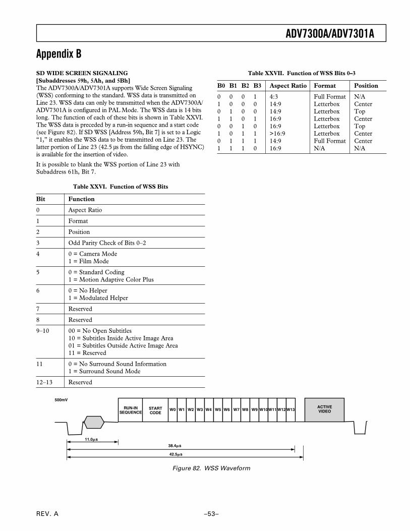
REV. A
ADV7300A/ADV7301A
–53–
Appendix BSD WIDE SCREEN SIGNALING[Subaddresses 59h, 5Ah, and 5Bh]The ADV7300A/ADV7301A supports Wide Screen Signaling(WSS) conforming to the standard. WSS data is transmitted onLine 23. WSS data can only be transmitted when the ADV7300A/ADV7301A is configured in PAL Mode. The WSS data is 14 bitslong. The function of each of these bits is shown in Table XXVI.The WSS data is preceded by a run-in sequence and a start code(see Figure 82). If SD WSS [Address 59h, Bit 7] is set to a Logic“1,” it enables the WSS data to be transmitted on Line 23. Thelatter portion of Line 23 (42.5 µs from the falling edge of HSYNC)is available for the insertion of video.
It is possible to blank the WSS portion of Line 23 withSubaddress 61h, Bit 7.
Table XXVI. Function of WSS Bits
Bit Function
0 Aspect Ratio
1 Format
2 Position
3 Odd Parity Check of Bits 0–2
4 0 = Camera Mode1 = Film Mode
5 0 = Standard Coding1 = Motion Adaptive Color Plus
6 0 = No Helper1 = Modulated Helper
7 Reserved
8 Reserved
9–10 00 = No Open Subtitles10 = Subtitles Inside Active Image Area01 = Subtitles Outside Active Image Area11 = Reserved
11 0 = No Surround Sound Information1 = Surround Sound Mode
12–13 Reserved
Table XXVII. Function of WSS Bits 0–3
B0 B1 B2 B3 Aspect Ratio Format Position
0 0 0 1 4:3 Full Format N/A1 0 0 0 14:9 Letterbox Center0 1 0 0 14:9 Letterbox Top1 1 0 1 16:9 Letterbox Center0 0 1 0 16:9 Letterbox Top1 0 1 1 >16:9 Letterbox Center0 1 1 1 14:9 Full Format Center1 1 1 0 16:9 N/A N/A
W0 W1 W2 W3 W4 W5 W6 W7 W8 W9 W10W11 W12 W13ACTIVEVIDEO
RUN-INSEQUENCE
STARTCODE
500mV
11.0s
38.4s
42.5s
Figure 82. WSS Waveform
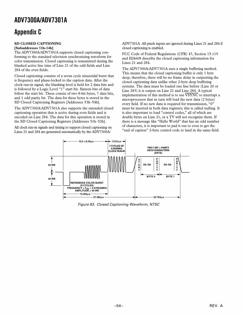
REV. A–54–
ADV7300A/ADV7301A
Appendix CSD CLOSED CAPTIONING[Subaddresses 51h–54h]The ADV7300A/ADV7301A supports closed captioning con-forming to the standard television synchronizing waveform forcolor transmission. Closed captioning is transmitted during theblanked active line time of Line 21 of the odd fields and Line284 of the even fields.
Closed captioning consists of a seven cycle sinusoidal burst thatis frequency and phase-locked to the caption data. After theclock run-in signal, the blanking level is held for 2 data bits andis followed by a Logic Level “1” start bit. Sixteen bits of datafollow the start bit. These consist of two 8-bit bytes, 7 data bits,and 1 odd parity bit. The data for these bytes is stored in theSD Closed Captioning Registers [Addresses 53h–54h].
The ADV7300A/ADV7301A also supports the extended closedcaptioning operation that is active during even fields and isencoded on Line 284. The data for this operation is stored inthe SD Closed Captioning Registers [Addresses 51h–52h].
All clock run-in signals and timing to support closed captioning onLines 21 and 284 are generated automatically by the ADV7300A/
ADV7301A. All pixels inputs are ignored during Lines 21 and 284 ifclosed captioning is enabled.
FCC Code of Federal Regulations (CFR) 47, Section 15.119and EIA608 describe the closed captioning information forLines 21 and 284.
The ADV7300A/ADV7301A uses a single buffering method.This means that the closed captioning buffer is only 1 bytedeep; therefore, there will be no frame delay in outputting theclosed captioning data unlike other 2-byte deep bufferingsystems. The data must be loaded one line before (Line 20 orLine 283) it is output on Line 21 and Line 284. A typicalimplementation of this method is to use VSYNC to interrupt amicroprocessor that in turn will load the new data (2 bytes)every field. If no new data is required for transmission, “0”must be inserted in both data registers; this is called nulling. Itis also important to load “control codes,” all of which aredouble bytes on Line 21, or a TV will not recognize them. Ifthere is a message like “Hello World” that has an odd numberof characters, it is important to pad it out to even to get the“end of caption” 2-byte control code to land in the same field.
START
PARITY
PARITY
D0–D6 D0–D6
10.5 0.25s 12.91s
7 CYCLES OF0.5035MHz
CLOCK RUN-IN
REFERENCE COLOR BURST(9 CYCLES)
FREQUENCY = FSC = 3.579545MHzAMPLITUDE = 40 IRE
50 IRE
40 IRE
10.003s27.382s 33.764s
BYTE 1BYTE 0
TWO 7-BIT + PARITYASCII CHARACTERS
(DATA)
Figure 83. Closed Captioning Waveform, NTSC
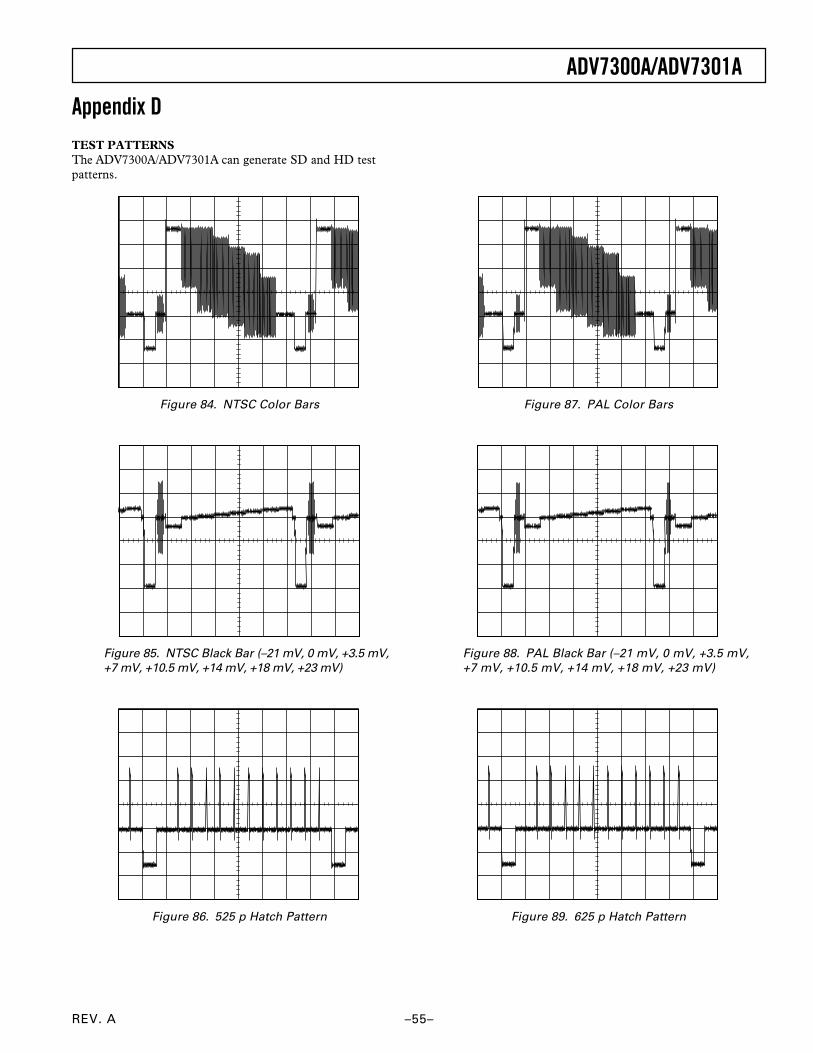
REV. A
ADV7300A/ADV7301A
–55–
Appendix DTEST PATTERNSThe ADV7300A/ADV7301A can generate SD and HD testpatterns.
Figure 87. PAL Color Bars
Figure 88. PAL Black Bar (–21 mV, 0 mV, +3.5 mV,+7 mV, +10.5 mV, +14 mV, +18 mV, +23 mV)
Figure 89. 625 p Hatch Pattern
Figure 84. NTSC Color Bars
Figure 85. NTSC Black Bar (–21 mV, 0 mV, +3.5 mV,+7 mV, +10.5 mV, +14 mV, +18 mV, +23 mV)
Figure 86. 525 p Hatch Pattern
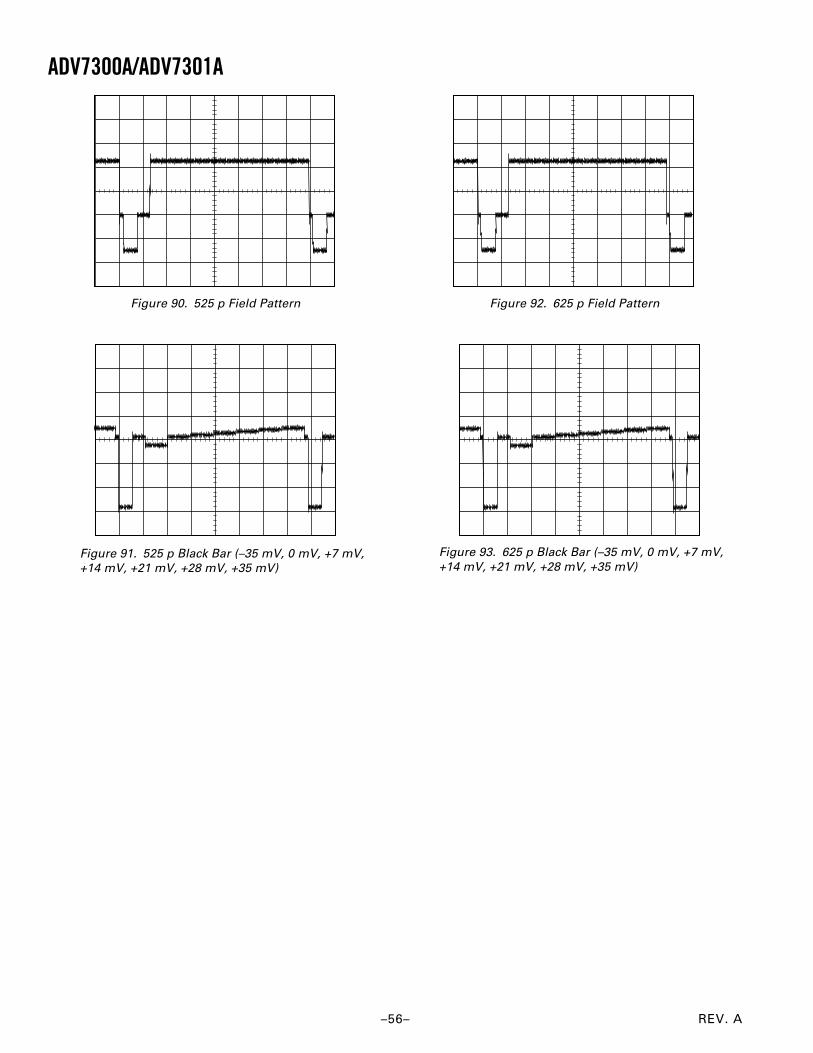
REV. A–56–
ADV7300A/ADV7301A
Figure 90. 525 p Field Pattern
Figure 91. 525 p Black Bar (–35 mV, 0 mV, +7 mV,+14 mV, +21 mV, +28 mV, +35 mV)
Figure 92. 625 p Field Pattern
Figure 93. 625 p Black Bar (–35 mV, 0 mV, +7 mV,+14 mV, +21 mV, +28 mV, +35 mV)
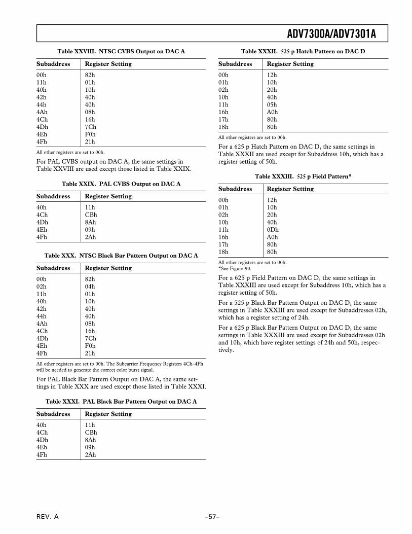
REV. A
ADV7300A/ADV7301A
–57–
Table XXVIII. NTSC CVBS Output on DAC A
Subaddress Register Setting
00h 82h11h 01h40h 10h42h 40h44h 40h4Ah 08h4Ch 16h4Dh 7Ch4Eh F0h4Fh 21h
All other registers are set to 00h.
For PAL CVBS output on DAC A, the same settings inTable XXVIII are used except those listed in Table XXIX.
Table XXIX. PAL CVBS Output on DAC A
Subaddress Register Setting
40h 11h4Ch CBh4Dh 8Ah4Eh 09h4Fh 2Ah
Table XXX. NTSC Black Bar Pattern Output on DAC A
Subaddress Register Setting
00h 82h02h 04h11h 01h40h 10h42h 40h44h 40h4Ah 08h4Ch 16h4Dh 7Ch4Eh F0h4Fh 21h
All other registers are set to 00h. The Subcarrier Frequency Registers 4Ch–4Fhwill be needed to generate the correct color burst signal.
For PAL Black Bar Pattern Output on DAC A, the same set-tings in Table XXX are used except those listed in Table XXXI.
Table XXXI. PAL Black Bar Pattern Output on DAC A
Subaddress Register Setting
40h 11h4Ch CBh4Dh 8Ah4Eh 09h4Fh 2Ah
Table XXXII. 525 p Hatch Pattern on DAC D
Subaddress Register Setting
00h 12h01h 10h02h 20h10h 40h11h 05h16h A0h17h 80h18h 80h
All other registers are set to 00h.
For a 625 p Hatch Pattern on DAC D, the same settings inTable XXXII are used except for Subaddress 10h, which has aregister setting of 50h.
Table XXXIII. 525 p Field Pattern*
Subaddress Register Setting
00h 12h01h 10h02h 20h10h 40h11h 0Dh16h A0h17h 80h18h 80h
All other registers are set to 00h.*See Figure 90.
For a 625 p Field Pattern on DAC D, the same settings inTable XXXIII are used except for Subaddress 10h, which has aregister setting of 50h.
For a 525 p Black Bar Pattern Output on DAC D, the samesettings in Table XXXIII are used except for Subaddresses 02h,which has a register setting of 24h.
For a 625 p Black Bar Pattern Output on DAC D, the samesettings in Table XXXIII are used except for Subaddresses 02hand 10h, which have register settings of 24h and 50h, respec-tively.
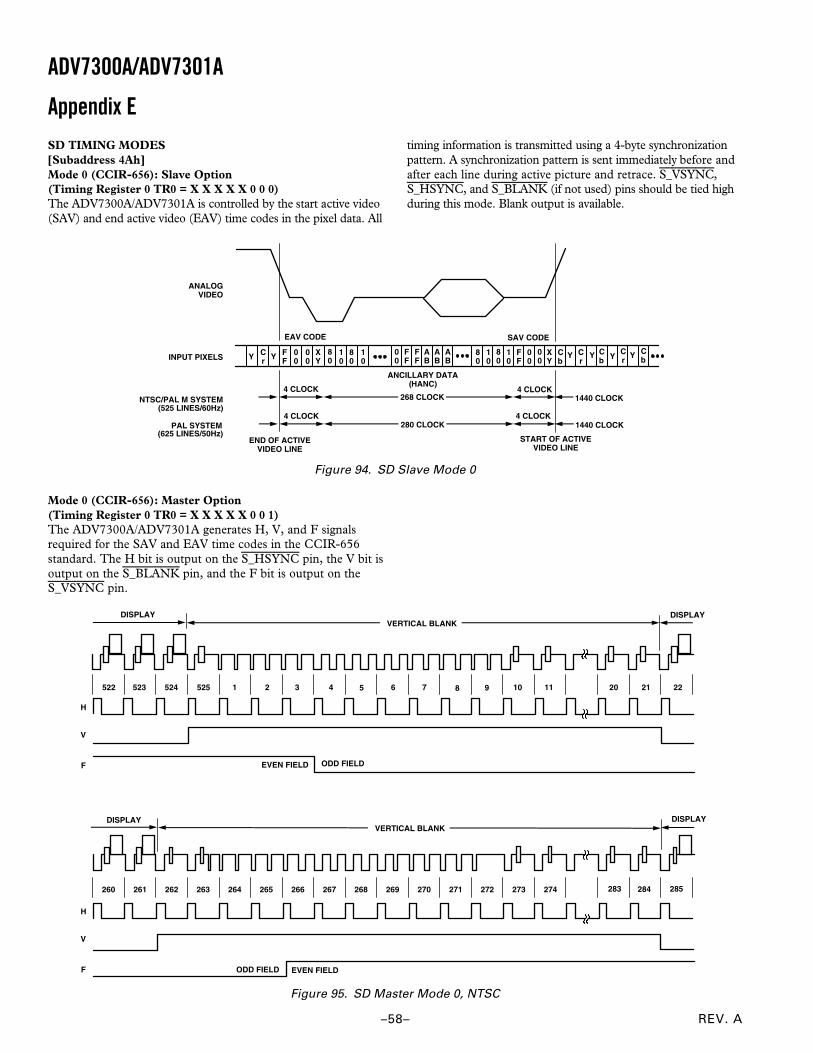
REV. A–58–
ADV7300A/ADV7301A
Appendix ESD TIMING MODES[Subaddress 4Ah]Mode 0 (CCIR-656): Slave Option(Timing Register 0 TR0 = X X X X X 0 0 0)The ADV7300A/ADV7301A is controlled by the start active video(SAV) and end active video (EAV) time codes in the pixel data. All
timing information is transmitted using a 4-byte synchronizationpattern. A synchronization pattern is sent immediately before andafter each line during active picture and retrace. S_VSYNC,S_HSYNC, and S_BLANK (if not used) pins should be tied highduring this mode. Blank output is available.
Y Cr Y F
F00
00
XY
80
10
80
10
FF
00
FF
AB
AB
AB
80
10
80
10
FF
00
00
XY
Cb
Y Cr
Cb
Y CbYC
r
EAV CODE SAV CODE
ANCILLARY DATA(HANC)
4 CLOCK 4 CLOCK 268 CLOCK 1440 CLOCK
4 CLOCK 4 CLOCK 280 CLOCK 1440 CLOCK
END OF ACTIVEVIDEO LINE
START OF ACTIVEVIDEO LINE
ANALOGVIDEO
INPUT PIXELS
NTSC/PAL M SYSTEM
PAL SYSTEM
Y
(525 LINES/60Hz)
(625 LINES/50Hz)
Figure 94. SD Slave Mode 0
Mode 0 (CCIR-656): Master Option(Timing Register 0 TR0 = X X X X X 0 0 1)The ADV7300A/ADV7301A generates H, V, and F signalsrequired for the SAV and EAV time codes in the CCIR-656standard. The H bit is output on the S_HSYNC pin, the V bit isoutput on the S_BLANK pin, and the F bit is output on theS_VSYNC pin.
522 523 524 525 1 2 3 4 5 6 7 8 9 10 11 20 21 22
DISPLAY DISPLAY VERTICAL BLANK
ODD FIELDEVEN FIELD
H
V
F
260 261 262 263 264 265 266 267 268 269 270 271 272 273 274 283 284 285
ODD FIELD EVEN FIELD
DISPLAY DISPLAY VERTICAL BLANK
H
V
F
Figure 95. SD Master Mode 0, NTSC
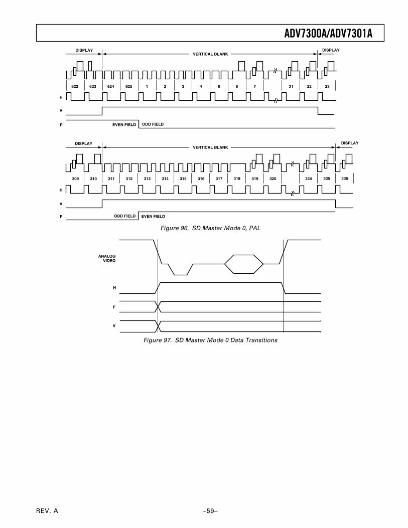
REV. A
ADV7300A/ADV7301A
–59–
622 623 624 625 1 2 3 4 5 6 7 21 22 23
DISPLAY DISPLAY VERTICAL BLANK
H
V
F ODD FIELDEVEN FIELD
309 310 311 312 314 315 316 317 318 319 320 334 335 336
DISPLAY DISPLAY VERTICAL BLANK
H
V
F ODD FIELD EVEN FIELD
313
Figure 96. SD Master Mode 0, PAL
ANALOGVIDEO
H
F
V
Figure 97. SD Master Mode 0 Data Transitions
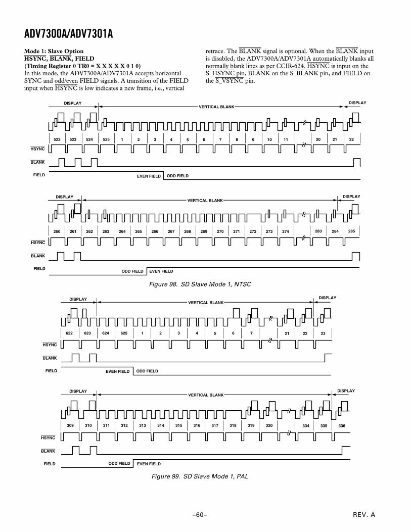
REV. A–60–
ADV7300A/ADV7301AMode 1: Slave OptionHSYNC, BLANK, FIELD(Timing Register 0 TR0 = X X X X X 0 1 0)In this mode, the ADV7300A/ADV7301A accepts horizontalSYNC and odd/even FIELD signals. A transition of the FIELDinput when HSYNC is low indicates a new frame, i.e., vertical
retrace. The BLANK signal is optional. When the BLANK inputis disabled, the ADV7300A/ADV7301A automatically blanks allnormally blank lines as per CCIR-624. HSYNC is input on theS_HSYNC pin, BLANK on the S_BLANK pin, and FIELD onthe S_VSYNC pin.
260 261 262 263 264 265 266 267 268 269 270 271 272 273 274 283 284 285
ODD FIELD EVEN FIELD
DISPLAY DISPLAY VERTICAL BLANK
522 523 524 525 1 2 3 4 5 6 7 8 9 10 11 20 21 22
DISPLAY DISPLAY VERTICAL BLANK
ODD FIELDEVEN FIELDFIELD
HSYNC
BLANK
FIELD
HSYNC
BLANK
Figure 98. SD Slave Mode 1, NTSC
622 623 624 625 1 2 3 4 5 6 7 21 22 23
DISPLAY VERTICAL BLANK
ODD FIELDEVEN FIELDFIELD
DISPLAY
309 310 311 312 313 314 315 316 317 318 319 334 335 336
DISPLAY VERTICAL BLANK
ODD FIELD EVEN FIELD
DISPLAY
320
HSYNC
BLANK
FIELD
HSYNC
BLANK
Figure 99. SD Slave Mode 1, PAL
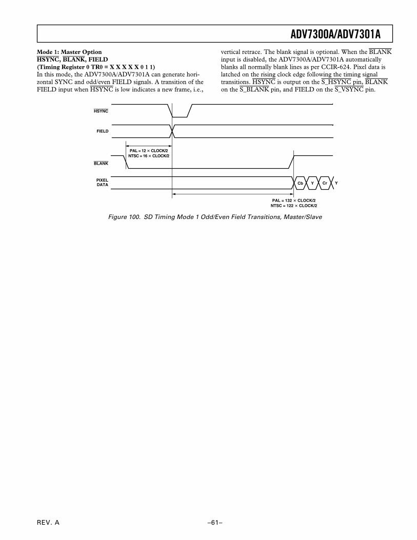
REV. A
ADV7300A/ADV7301A
–61–
Mode 1: Master OptionHSYNC, BLANK, FIELD(Timing Register 0 TR0 = X X X X X 0 1 1)In this mode, the ADV7300A/ADV7301A can generate hori-zontal SYNC and odd/even FIELD signals. A transition of theFIELD input when HSYNC is low indicates a new frame, i.e.,
vertical retrace. The blank signal is optional. When the BLANKinput is disabled, the ADV7300A/ADV7301A automaticallyblanks all normally blank lines as per CCIR-624. Pixel data islatched on the rising clock edge following the timing signaltransitions. HSYNC is output on the S_HSYNC pin, BLANKon the S_BLANK pin, and FIELD on the S_VSYNC pin.
FIELD
PIXELDATA
PAL = 12 CLOCK/2NTSC = 16 CLOCK/2
PAL = 132 CLOCK/2NTSC = 122 CLOCK/2
Cb Y Cr Y
HSYNC
BLANK
Figure 100. SD Timing Mode 1 Odd/Even Field Transitions, Master/Slave
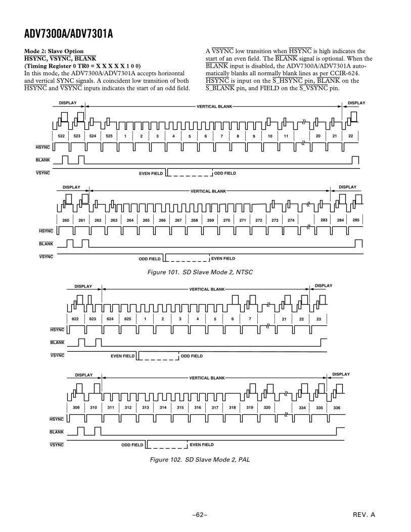
REV. A–62–
ADV7300A/ADV7301AMode 2: Slave OptionHSYNC, VSYNC, BLANK(Timing Register 0 TR0 = X X X X X 1 0 0)In this mode, the ADV7300A/ADV7301A accepts horizontaland vertical SYNC signals. A coincident low transition of bothHSYNC and VSYNC inputs indicates the start of an odd field.
A VSYNC low transition when HSYNC is high indicates thestart of an even field. The BLANK signal is optional. When theBLANK input is disabled, the ADV7300A/ADV7301A auto-matically blanks all normally blank lines as per CCIR-624.HSYNC is input on the S_HSYNC pin, BLANK on theS_BLANK pin, and FIELD on the S_VSYNC pin.
522 523 524 525 1 2 3 4 5 6 7 8 9 10 11 20 21 22
DISPLAY DISPLAY VERTICAL BLANK
ODD FIELDEVEN FIELD
260 261 262 263 264 265 266 267 268 269 270 271 272 273 274 283 284 285
ODD FIELD EVEN FIELD
DISPLAY DISPLAY VERTICAL BLANK
HSYNC
BLANK
VSYNC
HSYNC
BLANK
VSYNC
Figure 101. SD Slave Mode 2, NTSC
622 623 624 625 1 2 3 4 5 6 7 21 22 23
DISPLAY VERTICAL BLANK
ODD FIELDEVEN FIELD
HSYNC
BLANK
VSYNC
DISPLAY
309 310 311 312 313 314 315 316 317 318 319 334 335 336
DISPLAY VERTICAL BLANK
ODD FIELD EVEN FIELD
DISPLAY
320
HSYNC
BLANK
VSYNC
Figure 102. SD Slave Mode 2, PAL
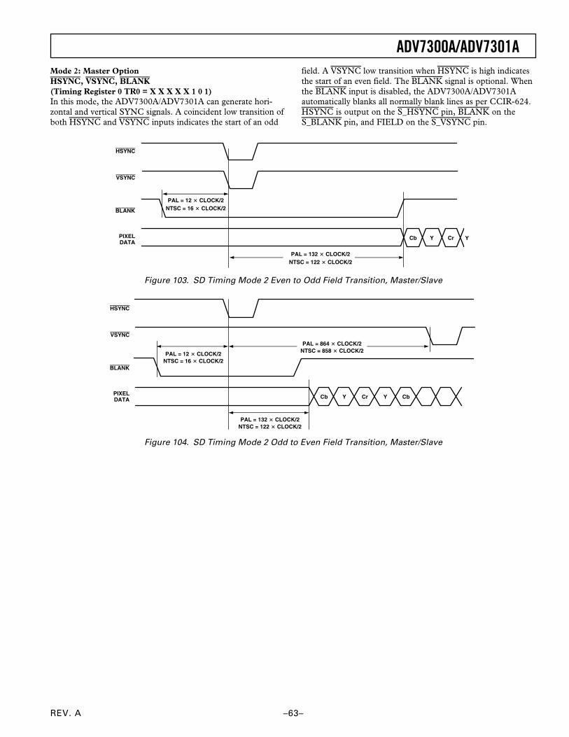
REV. A
ADV7300A/ADV7301A
–63–
Mode 2: Master OptionHSYNC, VSYNC, BLANK(Timing Register 0 TR0 = X X X X X 1 0 1)In this mode, the ADV7300A/ADV7301A can generate hori-zontal and vertical SYNC signals. A coincident low transition ofboth HSYNC and VSYNC inputs indicates the start of an odd
field. A VSYNC low transition when HSYNC is high indicatesthe start of an even field. The BLANK signal is optional. Whenthe BLANK input is disabled, the ADV7300A/ADV7301Aautomatically blanks all normally blank lines as per CCIR-624.HSYNC is output on the S_HSYNC pin, BLANK on theS_BLANK pin, and FIELD on the S_VSYNC pin.
PAL = 12 CLOCK/2NTSC = 16 CLOCK/2
PAL = 132 CLOCK/2 NTSC = 122 CLOCK/2
Cb Y Cr Y
HSYNC
VSYNC
BLANK
PIXELDATA
Figure 103. SD Timing Mode 2 Even to Odd Field Transition, Master/Slave
PAL = 864 CLOCK/2NTSC = 858 CLOCK/2
PAL = 132 CLOCK/2NTSC = 122 CLOCK/2
HSYNC
VSYNC
BLANK
PIXELDATA
PAL = 12 CLOCK/2NTSC = 16 CLOCK/2
Cb Y Cr Y Cb
Figure 104. SD Timing Mode 2 Odd to Even Field Transition, Master/Slave
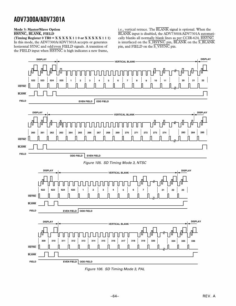
REV. A–64–
ADV7300A/ADV7301AMode 3: Master/Slave OptionHSYNC, BLANK, FIELD(Timing Register 0 TR0 = X X X X X 1 1 0 or X X X X X 1 1 1)In this mode, the ADV7300A/ADV7301A accepts or generateshorizontal SYNC and odd/even FIELD signals. A transition ofthe FIELD input when HSYNC is high indicates a new frame,
i.e., vertical retrace. The BLANK signal is optional. When theBLANK input is disabled, the ADV7300A/ADV7301A automati-cally blanks all normally blank lines as per CCIR-624. HSYNCis interfaced on the S_HSYNC pin, BLANK on the S_BLANKpin, and FIELD on the S_VSYNC pin.
260 261 262 263 264 265 266 267 268 269 270 271 272 273 274 283 284 285
ODD FIELD EVEN FIELD
DISPLAY DISPLAY VERTICAL BLANK
522 523 524 525 1 2 3 4 5 6 7 8 9 10 11 20 21 22
DISPLAY DISPLAY VERTICAL BLANK
ODD FIELDEVEN FIELD
HSYNC
BLANK
FIELD
HSYNC
BLANK
FIELD
Figure 105. SD Timing Mode 3, NTSC
622 623 624 625 1 2 3 4 5 6 7 21 22 23
DISPLAY VERTICAL BLANK
ODD FIELDEVEN FIELD
HSYNC
BLANK
FIELD
DISPLAY
309 310 311 312 313 314 315 316 317 318 319 334 335 336
DISPLAY VERTICAL BLANK
ODD FIELDEVEN FIELD
HSYNC
BLANK
FIELD
DISPLAY
320
Figure 106. SD Timing Mode 3, PAL
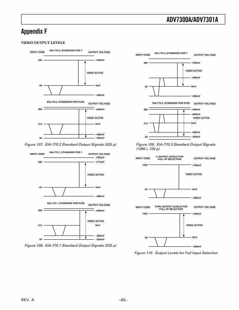
REV. A
ADV7300A/ADV7301A
–65–
Appendix FVIDEO OUTPUT LEVELS
INPUT CODE
940
64
EIA-770.2, STANDARD FOR Y
+700mV
OUTPUT VOLTAGE
0mV
–300mV
VIDEO ACTIVE
960
64
EIA-770.2, STANDARD FOR Pr/Pb
+350mV
OUTPUT VOLTAGE
0mV
–300mV
VIDEO ACTIVE
512
–350mV
Figure 107. EIA-770.2 Standard Output Signals (525 p)
INPUT CODE
940
64
EIA-770.1, STANDARD FOR Y
+714mV
OUTPUT VOLTAGE
0mV
–286mV
VIDEO ACTIVE
960
64
EIA-770.1, STANDARD FOR Pr/Pb
+350mV
OUTPUT VOLTAGE
0mV
–300mV
VIDEO ACTIVE
512
+782mV
–350mV
Figure 108. EIA-770.1 Standard Output Signals (525 p)
INPUT CODE
940
64
EIA-770.3, STANDARD FOR Y
+700mV
OUTPUT VOLTAGE
0mV
–300mV
VIDEO ACTIVE
+300mV
960
64
EIA-770.3, STANDARD FOR Pr/Pb
+350mV
OUTPUT VOLTAGE
0mV
–350mV
VIDEO ACTIVE
512
–300mV
+300mV
Figure 109. EIA-770.3 Standard Output Signals(1080 i, 720 p)
INPUT CODE
1023
64
Y–OUTPUT LEVELS FORFULL I/P SELECTION
+700mV
OUTPUT VOLTAGE
0mV
–300mV
VIDEO ACTIVE
1023
64
Pr/Pb–OUTPUT LEVELS FORFULL I/P SELECTION
+700mV
OUTPUT VOLTAGE
–300mV
VIDEO ACTIVE
0mV
INPUT CODE
Figure 110. Output Levels for Full Input Selection
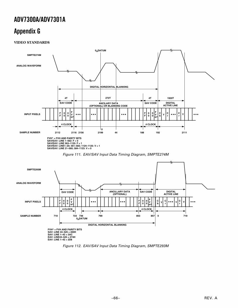
REV. A–66–
ADV7300A/ADV7301A
Appendix GVIDEO STANDARDS
FV
H*
FF
272T4T 4T 1920T
EAV CODE SAV CODE DIGITALACTIVE LINE
4 CLOCK 4 CLOCK
2112 2116 2156 21990
44 188 192 2111
00
00
00
00
FF
FV
H*
Cb
Cr
CrY YINPUT PIXELS
ANALOG WAVEFORM
SAMPLE NUMBER
FVH* = FVH AND PARITY BITSSAV/EAV: LINE 1–562: F = 0SAV/EAV: LINE 563–1125: F = 1SAV/EAV: LINE1–20; 561–583; 1124–1125: V = 1SAV/EAV: LINE 21–560; 584–1123: V = 0
SMPTE274M
DIGITAL HORIZONTAL BLANKING
ANCILARY DATA(OPTIONAL) OR BLANKING CODE
0HDATUM
Figure 111. EAV/SAV Input Data Timing Diagram, SMPTE274M
Y
EAV CODE ANCILLARY DATA(OPTIONAL)
SAV CODE DIGITALACTIVE LINE
719 723 736 799 853 0
FVH* = FVH AND PARITY BITSSAV: LINE 43–525 = 200HSAV: LINE 1–42 = 2ACEAV: LINE43–525 = 274HEAV: LINE 1–42 = 2D8
4 CLOCK 4 CLOCK
857 7190HDATUM
DIGITAL HORIZONTAL BLANKING
00
00
00
00
Cb
Cr
CrY Y
FV
H*
SMPTE293M
INPUT PIXELS
ANALOG WAVEFORM
SAMPLE NUMBER
FF
FF
FV
H*
Figure 112. EAV/SAV Input Data Timing Diagram, SMPTE293M
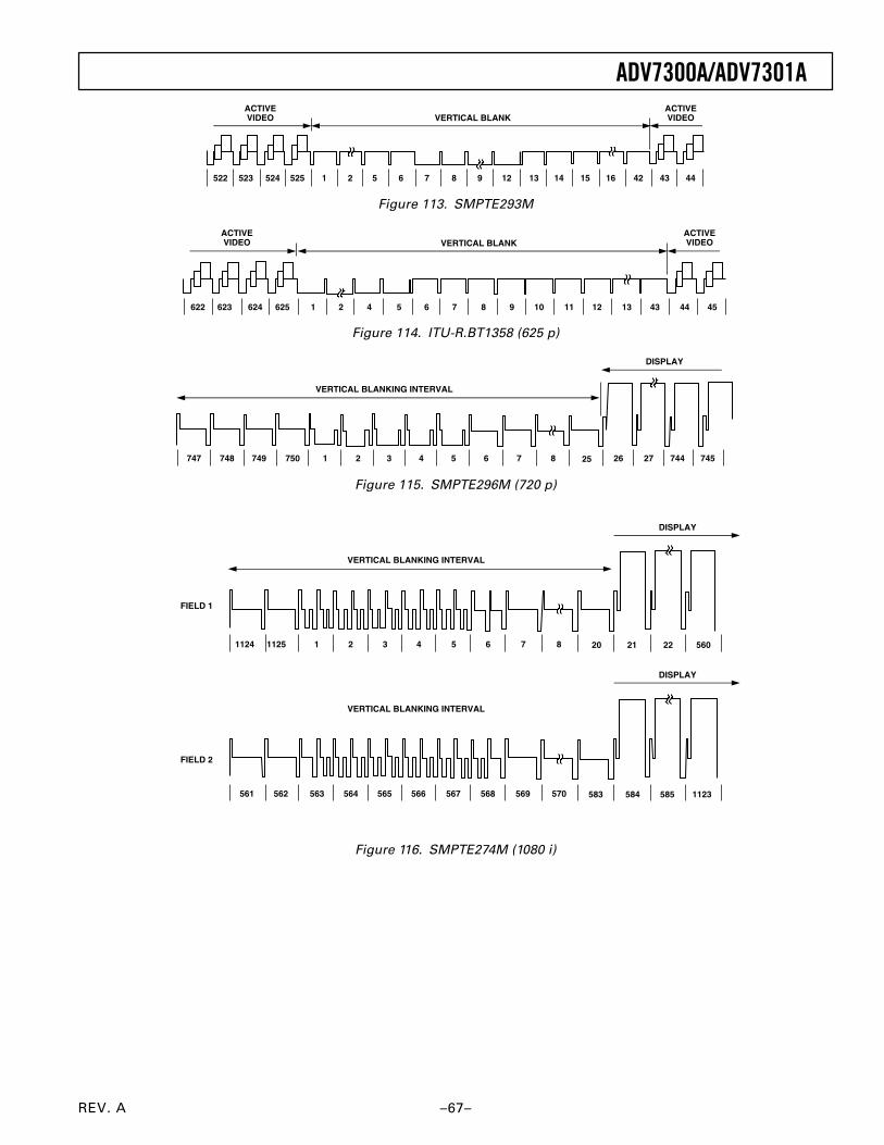
REV. A
ADV7300A/ADV7301A
–67–
VERTICAL BLANK
522 523 524 525 1 2 5 6 7 8 9 12 13 14 15 16 43 4442
ACTIVEVIDEO
ACTIVEVIDEO
Figure 113. SMPTE293M
VERTICAL BLANKACTIVEVIDEO
ACTIVEVIDEO
622 623 624 625 1 2 5 6 7 8 9 12 1310 11 43 44 454
Figure 114. ITU-R.BT1358 (625 p)
747 748 749 750 1 2 5 6 7 8 26 2725 744 7454
DISPLAY
3
VERTICAL BLANKING INTERVAL
Figure 115. SMPTE296M (720 p)
VERTICAL BLANKING INTERVAL
DISPLAY
1124 1125 1 2 5 6 7 8 2143 20 22 560
FIELD 1
VERTICAL BLANKING INTERVAL
DISPLAY
561 562 563 564 567 568 569 570 584566565 583 585 1123
FIELD 2
Figure 116. SMPTE274M (1080 i)
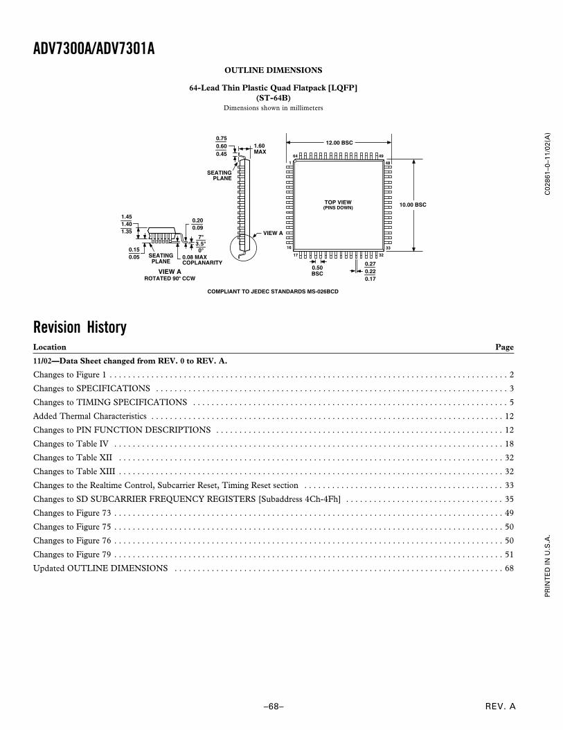
REV. A
C02
861–
0–11
/02(
A)
PR
INT
ED
IN U
.S.A
.
–68–
ADV7300A/ADV7301AOUTLINE DIMENSIONS
64-Lead Thin Plastic Quad Flatpack [LQFP](ST-64B)
Dimensions shown in millimeters
TOP VIEW(PINS DOWN)
1
16
17
33
32
48
4964
0.270.220.17
0.50BSC
10.00 BSC
1.60MAX
SEATINGPLANE
0.750.600.45
VIEW A7
3.50
0.20 0.09
1.45 1.40 1.35
0.150.05 0.08 MAX
COPLANARITY
VIEW AROTATED 90 CCW
SEATINGPLANE
12.00 BSC
COMPLIANT TO JEDEC STANDARDS MS-026BCD
Revision HistoryLocation Page
11/02—Data Sheet changed from REV. 0 to REV. A.
Changes to Figure 1 . . . . . . . . . . . . . . . . . . . . . . . . . . . . . . . . . . . . . . . . . . . . . . . . . . . . . . . . . . . . . . . . . . . . . . . . . . . . . . . . . . . . . . 2
Changes to SPECIFICATIONS . . . . . . . . . . . . . . . . . . . . . . . . . . . . . . . . . . . . . . . . . . . . . . . . . . . . . . . . . . . . . . . . . . . . . . . . . . . . 3
Changes to TIMING SPECIFICATIONS . . . . . . . . . . . . . . . . . . . . . . . . . . . . . . . . . . . . . . . . . . . . . . . . . . . . . . . . . . . . . . . . . . . . 5
Added Thermal Characteristics . . . . . . . . . . . . . . . . . . . . . . . . . . . . . . . . . . . . . . . . . . . . . . . . . . . . . . . . . . . . . . . . . . . . . . . . . . . . 12
Changes to PIN FUNCTION DESCRIPTIONS . . . . . . . . . . . . . . . . . . . . . . . . . . . . . . . . . . . . . . . . . . . . . . . . . . . . . . . . . . . . . . 12
Changes to Table IV . . . . . . . . . . . . . . . . . . . . . . . . . . . . . . . . . . . . . . . . . . . . . . . . . . . . . . . . . . . . . . . . . . . . . . . . . . . . . . . . . . . . 18
Changes to Table XII . . . . . . . . . . . . . . . . . . . . . . . . . . . . . . . . . . . . . . . . . . . . . . . . . . . . . . . . . . . . . . . . . . . . . . . . . . . . . . . . . . . 32
Changes to Table XIII . . . . . . . . . . . . . . . . . . . . . . . . . . . . . . . . . . . . . . . . . . . . . . . . . . . . . . . . . . . . . . . . . . . . . . . . . . . . . . . . . . . 32
Changes to the Realtime Control, Subcarrier Reset, Timing Reset section . . . . . . . . . . . . . . . . . . . . . . . . . . . . . . . . . . . . . . . . . . . 33
Changes to SD SUBCARRIER FREQUENCY REGISTERS [Subaddress 4Ch-4Fh] . . . . . . . . . . . . . . . . . . . . . . . . . . . . . . . . . . 35
Changes to Figure 73 . . . . . . . . . . . . . . . . . . . . . . . . . . . . . . . . . . . . . . . . . . . . . . . . . . . . . . . . . . . . . . . . . . . . . . . . . . . . . . . . . . . . 49
Changes to Figure 75 . . . . . . . . . . . . . . . . . . . . . . . . . . . . . . . . . . . . . . . . . . . . . . . . . . . . . . . . . . . . . . . . . . . . . . . . . . . . . . . . . . . . 50
Changes to Figure 76 . . . . . . . . . . . . . . . . . . . . . . . . . . . . . . . . . . . . . . . . . . . . . . . . . . . . . . . . . . . . . . . . . . . . . . . . . . . . . . . . . . . . 50
Changes to Figure 79 . . . . . . . . . . . . . . . . . . . . . . . . . . . . . . . . . . . . . . . . . . . . . . . . . . . . . . . . . . . . . . . . . . . . . . . . . . . . . . . . . . . . 51
Updated OUTLINE DIMENSIONS . . . . . . . . . . . . . . . . . . . . . . . . . . . . . . . . . . . . . . . . . . . . . . . . . . . . . . . . . . . . . . . . . . . . . . . 68