Embed Size (px)
Citation preview

IEEE Asian Solid-State Circuits Conference The 2nd
IEEE Asian Solid-State Circuits Conference The 3rd
A-SSCC 2007
12 - 14 November 2007 - Jeju, Korea
Advance Program
www.a-sscc.org
IEEE Asian Solid-State Circuits ConferenceThe 3rd

Tim
e
10:2
0-10
:40
10:4
0-12
:00
12:0
0-13
:00
13:0
0-14
:20
14:2
0-14
:40
14:4
0-16
:00
16:0
0-17
:00
18:0
0-20
:00
Adv
ance
d le
akag
e re
duct
ion
Tech
niqu
esR
usu
Ste
fan(
Inte
l)Lo
w e
nerg
y C
MO
S sy
stem
s fo
r bod
y se
nsor
net
wor
kan
d ub
iqui
tous
hea
lthca
reH
oi-J
un Y
oo(K
AIS
T)
SD
C E
xhib
its
Rec
eptio
n
Bre
ak
An
Intr
oduc
tion
to A
nalo
g to
Dig
ital C
onve
rter
Des
ign
– O
ld p
robl
ems
and
New
Cha
lleng
esD
avid
Rob
erts
on(A
nalo
g D
evic
es)
Silic
on m
m-w
ave
IC d
esig
nH
uei W
ang(
NTU
)
Lunc
h
[Tut
oria
l II]
A-S
SCC
200
7 C
onfe
renc
e Pr
ogra
m: N
ovem
ber 1
2 (M
on.),
200
7R
oom
1(R
amad
a B
allro
om 1
)R
oom
2(R
amad
a B
allro
om 2
)
An
Intr
oduc
tion
to A
nalo
g to
Dig
ital C
onve
rter
Des
ign
– O
ld p
robl
ems
and
New
Cha
lleng
esD
avid
Rob
erts
on(A
nalo
g D
evic
es)
Silic
on m
m-w
ave
IC d
esig
nH
uei W
ang(
NTU
)9:
00-1
0:20
On-
Site
Reg
istr
atio
n(9
am-6
pm)
[Tut
oria
l I]
[Tut
oria
l II]
[Tut
oria
l I]
[Tut
oria
l III]
[Tut
oria
l IV]
[Tut
oria
l III]
[Tut
oria
l IV]
Adv
ance
d le
akag
e re
duct
ion
Tech
niqu
esR
usu
Ste
fan(
Inte
l)Lo
w e
nerg
y C
MO
S sy
stem
s fo
r bod
y se
nsor
net
wor
kan
d ub
iqui
tous
hea
lthca
reH
oi-J
un Y
oo(K
AIS
T)
Bre
ak

Tim
eR
oom
1(R
amad
a B
allro
om 1
)R
oom
2(R
amad
a B
allro
om 2
)R
oom
3(R
amad
a B
allro
om 3
)R
oom
4(R
amad
a B
allro
om 4
)
9:00
-9:0
5
10:3
5-11
:05
12:4
5-13
:45
Sess
ion
1Po
wer
Effi
cien
t Circ
uits
and
Aya
tem
s
Sess
ion
2C
lock
& F
requ
ency
Gen
erat
ion
Sess
ion
3H
igh
Perf
orm
ance
Am
plifi
ers
and
Vara
ctor
-Les
s VC
O
Sess
ion
4Em
ergi
ng T
rend
s in
Pro
xim
ityIn
terf
ace
Co-
Cha
irs:
H. K
abuo
(Pan
ason
ic),
M.H
. Sun
woo
(Ajo
u U
niv.
)
Co-
Cha
irs: K
. Mas
hiko
(STA
RC
), S
.H.
Cho
(KA
IST)
Co-
Cha
irs: C
.-N. K
uo(N
at'l
Cha
o Tu
ngU
niv.
),B
.-S. K
im(S
ungK
yunK
wan
Uni
v.)
Co-
Cha
irs: C
.P. Y
ue(U
C S
anta
Bar
bara
),K
. Kot
ani(T
ohok
u U
niv.
)
15:5
0-16
:00
16:4
5-16
:50
19:0
0-21
:00
13:4
5-15
:50
“SoC
or S
iP :
Wha
t is
the
Bes
t Sol
utio
n in
IC B
usin
ess
for U
biqu
itous
Mob
ile P
latfo
rms?
”O
rgan
izer
: Tad
ahiro
Kur
oda(
Kei
o U
niv.
),Jou
ngho
Kim
(KA
IST)
Mod
erat
or: J
oung
ho K
im(K
AIS
T)
“Dis
play
Driv
er IC
’s: N
ext T
echn
olog
y an
d M
arke
t Tre
nds”
Org
aniz
er: T
adah
iro K
urod
a, K
eio
Uni
v.(J
apan
), O
h-K
yong
Kw
on(H
anya
ngU
niv.
)M
oder
ator
: Oh-
Kyo
ng K
won
(Han
yang
Uni
v.)
"How
to P
rese
nt a
Goo
d IS
SCC
Pap
er"
Dr.
Jan
Van
der
Spi
egel
(Pro
fess
or, U
nive
rsity
of P
enns
ylva
nia)
16:0
0-16
:45
16:5
0-18
:30
Bre
ak
Spec
ial T
alk
[Ple
nary
Spe
ech
1]
[Ple
nary
Spe
ech
2]
The
Stra
tegi
c C
onsi
dera
tions
for D
igita
l-TV
Syst
em-o
n-C
hip
Prod
ucts
Dr.
Hee
gook
Lee
(Pre
side
nt a
nd C
TO, L
G E
lect
roni
cs In
c., K
orea
)
Con
verg
ence
and
Div
erge
nce
in P
aral
lel f
or th
e U
biqu
itous
Era
Mr.
Sat
oru
Ito
(Cha
irman
and
CE
O, R
enes
as T
ach.
, Jap
an)
Ban
quet
Pane
l Dis
cuss
ion
Co-
Cha
irs: S
. Rus
u(In
tel),
K. W
ong(
Inte
l), B
. Jin
Yoo
n(E
TRI)
Co-
Cha
irs: S
. Wei
(Pho
enix
Mic
roel
ectro
nics
), J.
Kim
(Ram
bus)
SD
C /
Exh
ibits
Indu
stry
Pro
gram
Sess
ion
I-ILo
cal F
C T
rend
& C
ompu
ting
Circ
uits
Sess
ion
I-II
Stor
age
& H
igh
Spee
d In
terf
ace
Bre
ak
Lunc
h
11:0
5-12
:45
A-S
SCC
200
7 C
onfe
renc
e Pr
ogra
m: N
ovem
ber 1
3 (T
ue.),
200
7
Ope
ning
Bre
ak /
SD
C
9:05
-9:5
0
9:50
-10:
35

Tim
eR
oom
1(R
amad
a B
allro
om 1
)R
oom
2(R
amad
a B
allro
om 2
)R
oom
3(R
amad
a B
allro
om 3
)R
oom
4(R
amad
a B
allro
om 4
)R
oom
5(U
do H
all)
9:00
-9:4
5
9:45
-10:
30
10:3
0-11
:05
Sess
ion
5 - W
W"W
irele
ss &
Wire
line
Com
mun
icat
ion"
Sess
ion
6 - M
SP"M
ultim
edia
Sig
nal P
roce
ssin
g"Se
ssio
n 7
- MEM
"Mem
ory"
Sess
ion
8 - A
DC
"Hig
h-Pe
rfor
man
ce A
DC
s"
Sess
ion
9 - E
TA"E
mer
ging
Circ
uit
Tech
nolo
gies
and
Sen
sing
"
Co-
Cha
irs: T
. Che
ung(
Fujit
su),
J.P
ark(
GC
T S
emic
ondu
ctor
)C
o-C
hairs
: H. N
oda(
Ren
esas
), R
.W
oo(L
G E
lect
roni
cs)
Co-
Cha
irs: J
.-B. L
ee(S
amsu
ng),
T.Y
abe(
Tosh
iba)
Co-
Cha
irs: S
.-H. L
ee(S
ogan
g U
niv.
),M
. Ots
uka(
Ren
esas
)C
o-C
hairs
: H. M
izun
o(H
itach
i),A
. Kes
hava
rzi(I
ntel
)
13:1
0-14
:10
Sess
ion
10 -
MSP
"Mix
ed-S
igna
l Circ
uits
for
Com
mun
icat
ions
"
Sess
ion
11 -
DC
S"D
igita
l Circ
uits
for P
ower
, Clo
ckan
d N
oise
"
Sess
ion
12 -
RF
"Fre
guen
cy D
ivid
er a
nd M
ultip
lier"
Sess
ion
13 -
AD
C"H
igh-
Perf
orm
ance
AD
Cs
and
Pow
er M
anag
emen
t Circ
uits
"
Co-
Cha
irs: K
. Arim
oto(
Ren
esas
),O
.-K. K
won
(Han
yang
Uni
v.)
Co-
Cha
irs: M
. Ike
da(U
niv.
of T
okyo
),K
.-S. M
in(K
ookm
in U
niv.
)C
o-C
hairs
: R. K
im(M
atsu
shita
), H
.Lu
ong(
HK
US
T)C
o-C
hairs
: H. O
node
ra(K
yoto
Uni
v.),
J. C
hoi(U
niv.
of S
eoul
)
16:1
5-16
:30
Sess
ion
14 -
MSP
"Gra
phic
s an
d R
econ
figur
able
Proc
essi
ng"
Sess
ion
15 -
WW
/AD
C"M
ulti-
Gig
abit
Rec
eive
rTe
chni
ques
"
Sess
ion
16 -
RF
"Osc
illat
ors
and
PLL"
Sess
ion
17 -
AD
C"A
nalo
g Te
chni
ques
"
Co-
Cha
irs: T
. Shi
miz
u(R
enes
as),
Y. P
ark(
Sam
sung
)C
o-C
hairs
: C. W
. Kim
(Kor
ea U
niv.
), M
.N
agat
a(K
obe
Uni
v.)
Co-
Cha
irs: H
. Shi
n(K
wan
gwoo
nU
niv.
),M
. Fuj
ishi
ma(
Uni
v. o
f Tok
yo)
Co-
Cha
irs: K
. Iiz
uka(
Sha
rp),
S.I.
Liu
(Nat
'l Ta
iwan
Uni
v.)
16:3
0-18
:35
14:1
0-16
:15
11:0
5-13
:10
Bre
ak
Lunc
h
Bre
ak
Exhi
bits
A-S
SCC
200
7 C
onfe
renc
e Pr
ogra
m: N
ovem
ber 1
4 (W
ed.),
200
7
[Ple
nary
Spe
ech
3] "
Rec
ent B
usin
ess
Mod
els
and
Tech
nolo
gy T
rend
s an
d Th
eir I
mpa
ct o
n th
e Se
mic
ondu
ctor
Indu
stry
" (D
r. Ja
ckso
n H
u, C
hairm
an, U
MC
, Tai
wan
)
[Ple
nary
Spe
ech
4] "
Ana
log
Des
ign
Cha
lleng
es in
Nan
omet
er C
MO
S Te
chno
logi
es"
(Dr.
Wily
San
sen,
Pro
fess
or, K
atho
lieke
Uni
v. L
euve
n., B
elgi
um)
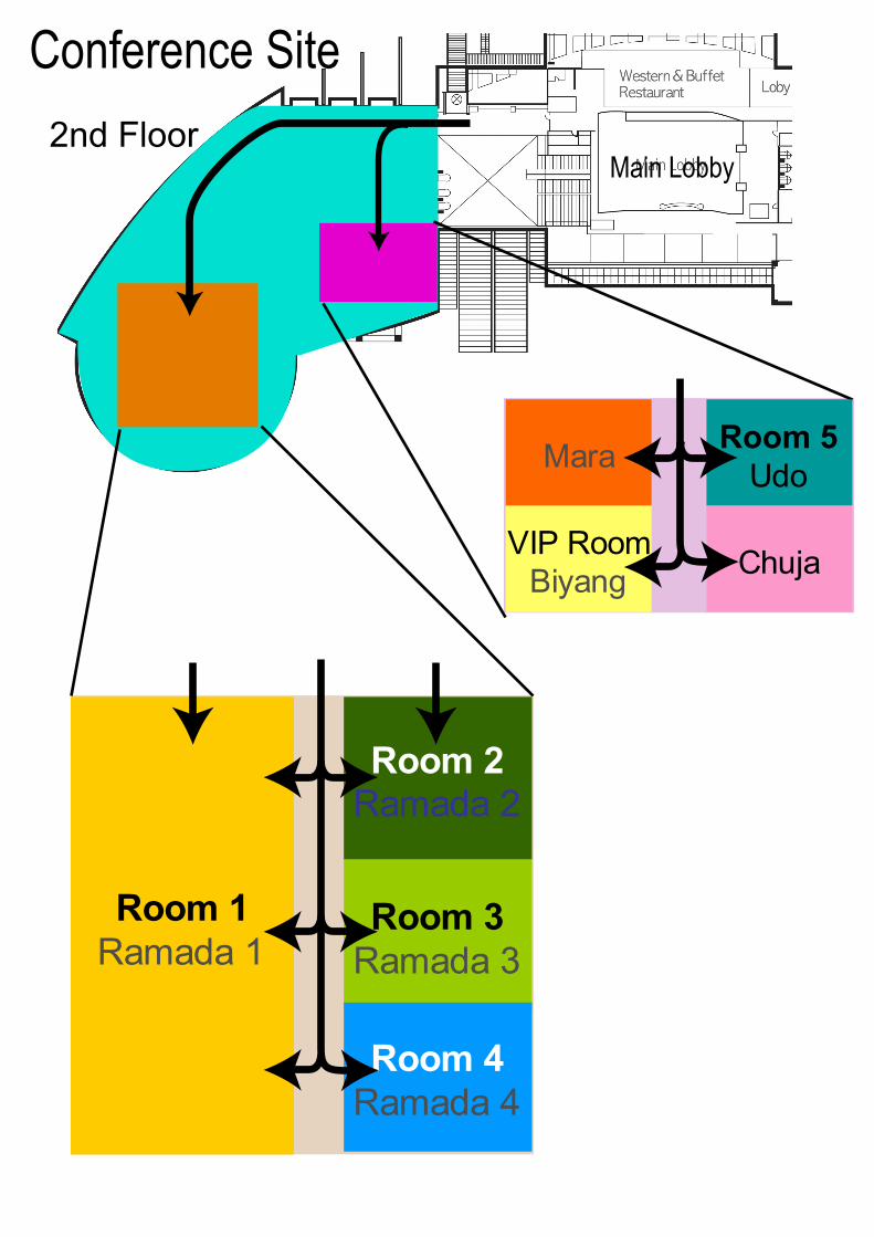
2nd FloorMain Lobby
Conference Site
Room 1Ramada 1
Room 2Ramada 2
Room 3Ramada 3
Room 4Ramada 4
Mara
VIP RoomBiyang
Room 5Udo
Chuja

Session P-1 Plenary Speech 1 November 13, 2007 (Tue.)
P-1 9:05-9:50
The Strategic Considerations for Digital-TV System-on-Chip Products Heegook Lee(LG Electronics Inc.)
Abstract: The delivery channels for digital TV broadcasting have been diversified: terrestrial, cable, satellite, beyond 3G cellular band and now over the internet. On the physical dimension, popularity of larger screen flat TV’s are rapidly growing, while mobile TV technology brought TV viewing to cell phones with QVGA screens. The flexibility of when to watch the programs has been enhanced by PVR technology and set-top boxes with push technology services. And IPTV VOD services offer more flexibility to consumers when and what to watch. Large screen flat TV’s are also used for Home Theater environments for Full HD contents. All these developments have occurred within just a few years, and the tasks of developing System-on-Chip (SoC) solutions for the various applications are very challenging. This paper will explore the strategic considerations chip developers have to employ to create the most competitive Digital TV SoC technology and products.
Session P-2 Plenary Speech 2 November 13, 2007 (Tue.)
P-2 9:50-10:35
Convergence and Divergence in Parallel for the Ubiquitous Era Satoru Ito(Renesas Tech. Corp.)
Abstract: After having enjoyed the years of staggering growth in the 90’s, the semiconductor industry is being matured. Today, it is still a growing industry, at a slower pace, as it continues to expand its reach to cover a growing number of all industries. While miniaturization is still an important consideration for many semiconductor manufacturers, the multitude of complex technology and economical scale limitations are posing as new challenges. Today, there is no single driving force to fuel the growth of the semiconductor industry. Under this new paradigm, it is important re-evaluate the business model of the semiconductor industry, together with two keywords, “Convergence” and Divergence.” “Convergence” enables utilization of various application contents beyond time and space, allowing consumers to access data from anywhere, anytime. On the other hand, “Divergence” accelerates segmentation, bringing solutions such as electronics systems tailored for each individual need and widely distributed networked systems. In the ubiquitous era, these seemingly contradicting elements become the foundation for establishing a new business model. Given the change, what is required for Technology is also changing. What the industry really needs is a system-centric innovation approach centered on software, to enable delivery of a wide spectrum of applications, rather than a conventional hardware-centric approach. In my presentation, I’ll discuss how to enable such innovations as well as how to overcome other challenges the industry will be facing in the next several years.

Session P-3 Plenary Speech 3 November 14, 2007 (Wed.)
P-3 9:00-9:45
Recent Business Models and Technology Trends and Their Impact on the Semiconductor Industry Jackson Hu(UMC)
Abstract: The semiconductor industry is evolving. IDMs are moving to a “fab-lite” or fabless approach due to skyrocketing development costs for advanced technologies. However, a fab-lite strategy isn’t simple to execute. Fabless companies also face pressures caused by limited design resources and their desire for multiple manufacturing sources. New materials and equipment have led to uncertainties that threaten Moore’s Law, and design for manufacturability (DFM) has become increasingly critical. Although smaller geometries allow an entire system on a single chip, designers may not have taken full advantage of this in their rush to keep up with Moore’s law. The design, EDA and manufacturing communities must re-examine their approach. Generally speaking, there is a capacity surplus for older production technologies. Newcomers who jumped into the foundry industry have realized that fab construction is not that difficult, however, filling the capacity and operating profitably is extremely challenging. In summary, the dynamics of IDM, fabless design companies and foundries will be examined.
Session P-4 Plenary Speech 4 November 14, 2007 (Wed.)
P-4 9:45-10:30
Analog Design Challenges in Nanometer CMOS Technologies Willy Sansen(Katholieke Univ. Leuven)
Abstract: In nanometer CMOS technologies, several new effects emerge due to short channel-length effects. Some important ones are velocity saturation and gate leakage currents. As a result improved transistor models are required to allow accurate prediction of analog circuit performance. The transconductance and speed are both limited by velocity saturation. Also noise and mismatch suffer from smaller channel lengths, as a result of the thinner gate oxides used. Moreover the supply voltage is reduced to values below 1 volt, creating new challenges for analog circuit design. This presentation provides a review of these model parameters. It is followed by an overview of amplifiers/filters configurations with both Gate and Bulk drives. Current amplifiers are compared to voltage amplifiers in terms of speed and input noise. A large variety of sub-1 volt circuits for different applications are then presented for sake of illustration.

Session I-I Industry Session I: Local FC Trend & Computing Circuits November 13, 2007 (Tue.) 11:05-12:45
Session Co-Chairs: Stefan Rusu(Intel), Keng Wong(Intel), Byoung Jin Yoon(ETRI) I-I-1 11:05-11:30
Where is Korea's Fabless Semiconductor Industry Headed? James Hwang (IT-SoC Association, Korea)
Abstract: Riding on the boom of handset and system display manufacturing at home, Korea's fabless semiconductor industry has made a sharp increase by leaps and bounds. The sales revenue of the fabless semiconductor companies more than doubled to 1.5 trillion Korean won in 2006, compared to 650 billion Korean won in 2003. Marking an annual average growth of 32 percent, the industry is now around the corner of global jump: by overcoming such issues as a broad range of portfolio set-up, business volume expansion through M&A, market diversification, etc. I-I-2 11:30-11:55
Penryn: 45nm Next Generation Intel Core Microarchitecture Varghese George (Intel Corp., USA)
Abstract: This paper/presentation will discuss Intel's upcoming Penryn (codename) family of processors which are based on Intel’s leading 45nm High-k metal gate silicon process. The paper will cover 1) an overview of the new 45 nm process technology and its benefits utilized in Penryn 2) an overview of the major new architectural features such as the Fast Radix-16 Divider, the new Intel SSE4 instructions and other microarchitecture enhancements for improved performance. 3) Advanced Power management features such as Deep Power Down Technology and Enhanced Intel Dynamic Acceleration Technology 4) Some of the physical design implementation challenges and innovations including efficient organization of the larger L2 cache, Low Power techniques used in the design, Clock and Power distribution, Design for Test and Design for Debug techniques and features, and the Packaging technology used in various family of Penryn products. I-I-3 11:55-12:20
Design of a 90nm 4-CPU 4320MIPS SoC with Individually Managed Frequency and 2.4GB/s Multi-master On-chip Interconnect
Osamu Nishii, Itaru Nonomura, Yutaka Yoshida, Kiyoshi Hayase, Shin'ichi Shibahara (Renesas Tech. Corp., Japan), Yoshitaka Tsujimoto, Masashi Takada (Hitachi Ltd., Japan), and Toshihiro Hattori (Renesas Tech. Corp., Japan)
Abstract: We have developed a 97.6mm2 SoC that includes four SuperH architecture CPUs and DDR-2 controller with 90nm CMOS for high-performance embedded applications. These four 600MHz CPUs are identical and each has floating point, 32/32KB cache memory, and 152KB local memory. CPUs totally achieve performance of 4320MIPS. Main on-chip 300MHz 64bit bus manages processors access and another dedicated connection holds cache coherency operation. Considering varying processing load, this chip targets both low power consumption (proportional to processing load), and constant on-chip bandwidth. Each processor can be operated different frequencies while keeping on-chip bus frequency

constant. With utilizing this individual core clock distribution scheme, the following designs have been developed: (i) frequency transition control that permits on-chip bus access of other bus master, (ii) light-sleep mode that maintains cache coherency control, (iii) cache snoop control logic that holds cache coherency between multiple frequency processors. The main on-chip interconnect (bus) connects four-processor and other on-chip IPs. The numbers of access master and access slave increase due to processor number. This on-chip bus specification and logic implementation technique achieve 300MHz multi-master operation. I-I-4 12:20-12:45
The Niagara2: A Highly Threaded Power Efficient Sparc SOC Gregory Grohoski, Robert Golla, Manish Shah, Paul Jordan, Jeffrey Brooks, Christopher Olson, Mark Luttrell, and Jama Barreh (Sun Microsystems, USA)
Abstract: Niagara2 is a second generation multi-core, multi-threaded 64b Sparc SOC. Niagara2 supports concurrent execution of 64 threads by utilizing eight, 8-threaded Sparc cores which communicate with a 4MB, 8-bank L2 cache through a high bandwidth crossbar. Niagara2 delivers twice the throughput of its predecessor, the UltraSparc T1, in essentially the samepower envelope. Each Sparc core includes two integer execution units, a dedicated floating-point and graphics unit, and a cryptographic unit. Niagara2 has a peak floating-point throughput performance of 11.2 GFLOPS/s. Niagara2 contains one x8 PCI-Express channel, two 10G Ethernet ports with XAUI interfaces, and four memory controllers each controlling 2 FBDIMM channels. Niagara2 achieves a peak memory bandwidth in excess of 60GB/s. Niagara2 is fabricated in an 11 metal, 1.1V, triple-Vt CMOS process. Niagara2 has ~500M transistors on a 342 mm2 die with a power consumption of 84W at 1.4GHz.
Session I-II Industry Session II: Storage & High Speed Interface November 13, 2007 (Tue.) 11:05-12:45
Session Co-Chairs: Shaojun Wei(Phoenix Microelectronics), Jaeha Kim(Rambus) I-II-1 11:05-11:30
SSC - A New Generation of Smart Controller for Mobile Storage Yanhui Yang, Muhua Han, Sudong Yu, and Shaojun Wei (Phoenix Microelectronics, China)
Abstract: Personal information storage and data processing are two of the key issues in mobile device product development. SSC give a new solution to solve these handicaps on account of that it is different from traditional SD card, MMC card and USB device. It tries to integrate high performance calculation, large volume memory and some popular flash card interfaces together into one chip, which leads to a new generation of smart controller for mobile storage. SSC can be used in mobile phones, digital camera, and other electronic devices which need not only large storage but also data processing and information management ability. Mega-Byte class SIM is a typical usage. It can provide an attractive and profitable Value-Added-Service (VAS) platform to telecom carriers. Assisted by the new SIM, the mobile phone can largely expand and strengthen it’s user experience, WEP service is a excellent practice benefit from it’s GUI system to provide renewable applications. A programmable chip platform and flexible software system are absolutely necessarily. This paper will focus on these topics and give some key discussions on
smart controller chip and major application software design technology. One successfully developed SoC will be presented also in this paper. I-II-2 11:30-11:55
A PCI-Express Gen2 Transceiver with Adaptive 2-Tap DFE for Up to 12-meter External Cabling Tse-Hsien Yeh, Wei-Yu Wang, Wen-Liang Wang, Yu-Hong Lin, Ying-Lien Cheng, Tsung-Hsin Chou, and Jyhfong Lin (VIA Technologies, Inc., Taiwan)
Abstract: The most updated specification of PCI-Express External Cabling 1.0 only specifies Gen1 (2.5Gbps) for short-reach usage. This proposed transceiver architecture not only increases the link rate from Gen1 to Gen2 (5Gbps), but also extends link range from short-reach to long-reach using a 12-meter 26AWG cable. The S21 of such a cable is -20dB at 2.5GHz. The new receiver achieves jitter tolerance at the far-end terminal followed by such a cable is 0.76UI, with a random jitter of 0.31UI, under the BER of 10-12. This design has been fabricated in TSMC 80nm CMOS process, with the die area of 0.4mm2 for each lane. I-II-3 11:55-12:20
A Low Power and Highly Reliable 400Mbps 512M Mobile DDR SDRAM with On-chip Distributed ECC
Saeng-Hwan Kim, Won-Oh Lee, Jung-Ho Kim, Seong-Seop Lee, Sun-Young Hwang, Chang-Il Kim, Tae-Woo Kwon, Bong-Seok Han, Sung-Kwon Cho, Dae-Hui Kim, Jae-Keun Hong, Min-Yung Lee, Sung-Wook Yin, Hyeon-Gon Kim, Jin-Hong Ahn, Yong-Tark Kim, Yo-Hwan Koh, Joong-Sik Kih(Hynix Semiconductor Inc., Korea)
Abstract: A 512Mb Mobile SDRAM with on-chip error correction code (ECC), which supports either single or double data rate and operates on a 1.8V power supply, is developed. The ECC circuit is optimized with respect to the increase in the chip area and the access-time penalty. The ratio of ECC area increase compared with the conventional mobile DRAM is 15%, and the fast comparing circuits of built-in Hamming code technique check 12 cell data simultaneously and satisfy the specification of 400Mbps DDR SDRAM. The self refresh period at standby state shows about 6 times increase reducing the self refresh current to be less than 100μA at 85°C. The newly adopted DCCS in the ECC, which is resistant from the clustered failures, and the concurrent row redundancy produce a synergistic fault-tolerance effect. The reliability could be 106 times higher by the ECC than that of the conventional DRAM. I-II-4 12:20-12:45
Value Creation in SOC/MCU applications by Embedded Non-Volatile Memory Evolution Masahiro Hatanaka and Hideto Hidaka(Renesas Technology Corporation, JAPAN)]
Abstract: Flash-MCU, Micro-Controller with Embedded Flash Memory storage (eFlash), has seen a tremendous up-surge in real-time control application markets, with assumed 15-20% CAGR. The programmable code storage provided by eFlash contributes to production cost reduction and real-time adaptive control applications, realizing a value innovation with remarkable cost/value advantage. The diversified advanced eFlash technology for converging flash-MCU products challenges new market drivers like automotive and smart-IC cards. Current status and future directions of flash-MCU with

evolution of LSI by programmability functions are also reviewed.
Panel Discussions November 13, 2007 (Tue.) 16:50-18:30
Panel-1 SoC or SiP : What is the Best Solution in IC Business for Ubiquitous Mobile Platforms?
Organizer: Tadahiro Kuroda(Keio Univ.), Joungho Kim(KAIST) Moderator: Joungho Kim(KAIST) Panelists / position:
C. Kim(Samsung) Wafer-Level 3D Chip-Stacking M. Aoyagi(AIST) Wafer-Level 3D Chip-Stacking T. Akazawa(Renesas) SiP and 3D Packaging C. H. Lee(Amkor) SiP and 3D Packaging C. P. Hung(ASE) SiP and 3D Packaging A. Lu(SIMTECH) SiP and 3D Packaging S. Y. Oh(ETRI) Design Issues and Emerging Technologies M. Nomura(NEC) Design Issues and Emerging Technologies T. L. Wu(NTU) Design Issues and Emerging Technologies
Abstract: Non-recurring engineering cost and development cycle for chip design and software are rapidly increasing. In addition, we are experiencing a piercing pressure for IC system packaging solutions with an extremely small form-factor. However, only a handful of big projects can pay you with the conventional approaches. Middle and small volume products may require a new solution. Could it be programmable SoC devices such as FPGA and Reconfigurable Processor, integrated with analog, RF, and memory circuits? Or, could it be SiP approach where commodity chips rather than IP’s are integrated into a tiny 3D package with integrated passives and antenna? We can discuss cost, time-to-market, size, flexibility, and power consumption of these two approaches to provide the best IC system solution for ubiquitous mobile platform. Panel-2 Display Driver IC’s: Next Technology and Market Trends
Organizer: Tadahiro Kuroda(Keio Univ.), Oh-Kyong Kwon(Hanyang Univ.) Moderator: Oh-Kyong Kwon(Hanyang Univ.) Panelists / position:
M.-H. Lee(Samsung) IC maker H. Hayama(NEC Electronics) IC maker Y. Yokota(Renesas) IC maker Y-L Chen(Himax) IC maker S. Lai(Solomon Systech) IC maker H.-K. Chung, Samsung SDI OLED C. T. Liu(AUO) Panel maker (LCD) T. Nishibe(TMD) Panel maker (LCD) M. Okamoto(Sharp) (LCD) R. Hattori(Kyushu Univ. (Academia)

Abstract: The flat panel display industry has enjoyed tremendous growth over the past 15 years and has created many applications such as mobile displays, note PC’s, monitors, and large-size digital TV’s. The objective of this panel is to describe the technology and market trends for advances in display system and display driver IC design. In mobile display, we will discuss the technical issues on circuit integration of a-Si TFT and poly-Si TFT for low-cost and additional embedded functions such as touch screen, ambient brightness sensing and finger print recognition, and etc. and market trends among a-Si TFT-LCD, LTPS TFT-LCD and OLED. For large-size displays, we will discuss the issues of display system and chip design for 10-bit or higher-bit gray scale, optimum panel resolution(Full-HD or higher) for home TV, and how much increase the number of frame rates for higher image quality. Also, we will discuss how display and semiconductor industries make ‘win-win’ situation.

Session 1 Power Efficient Circuits and Systems November 13, 2007 (Tue.) 13:45-15:50
Session Co-Chairs: Hideyuki Kabuo(Panasonic), Myung H. Sunwoo(Ajou Univ.) 1-1 13:45-14:10
Performance and Power Evaluation of SH-X3 Multicore System Masashi Takada (Hitachi Ltd., Japan), Shinichi Shibahara, Kiyoshi Hayase, Tatsuya Kamei, Yutaka Yoshida (Renesas Tech. Corp., Japan), Kiwamu Takada (Hitachi ULSI Systems Co. Ltd., Japan), Naohiko Irie (Hitachi Ltd., Japan), Osamu Nishii, and Toshihiro Hattori (Renesas Tech. Corp., Japan)
Abstract: We have developed an embedded processor that supports asymmetric multiple processor (AMP), symmetric multiple processor (SMP), and an AMP/SMP hybrid system. It contains four SH-X3 cores used to enhanced cache coherency from that obtained using an SH-X2 core. In this paper, we evaluate the following three techniques to improve the processing performance and reduce the power consumption in parallel processing in the processor. The first technique is snoop controller (SNC) to improve cache coherency performance. The performance overhead by snoop is decreased up to 0.1% when SPLASH-2 is executed. The second technique is detection and resolution of synonym problems so that we may not use the page coloring for page table management. The processes handling time in Linux is reduced by 29.4% compared with the case solved the problem with software. The third technique is the individual core clock frequency and the light sleep mode which is used to maintain the cache coherency even when the cores are stopped, to reduce the power consumption. The energy is decreased by 5.2% and 4.5%, respectively. As a result, the SH-X3 core achieved a performance that has a scalability proportional to 0.72-0.93 times the number of cores and a power saving of 4.5-44.0% without increasing the execution time. 1-2 14:10-14:35
Implementation of Memory-Centric NoC for 81.6 GOPS Object Recognition Processor Donghyun Kim, Kwanho Kim, Joo-Young Kim, Seungjin Lee, and Hoi-Jun Yoo (KAIST, Korea)
Abstract: An 81.6 GOPS object recognition processor based on Memory-Centric NoC (MC-NoC) is implemented in a 0.18um CMOS technology. The MC-NoC facilitates data transactions among 10 SIMD Processing Elements (PEs) by exploiting 8 Visual Image Processing (VIP) memories. The 10 PEs implement special SIMD instructions to perform Gaussian filtering at 16 GOPS. The 8 VIP memories provide one cycle local maximum pixels search operation performing 65.6 GOPS. The chip dissipates 1.4W at 200 MHz operating frequency. 1-3 14:35-15:00
Low hardware complexity key equation solver chip for Reed-Solomon decoders Jaehyun Baek and Myung H. Sunwoo (Ajou Univ., Korea)
Abstract: This paper proposes a new simplified degree computationless modified Euclid’s algorithm (S-DCME) and its architecture for Reed-Solomon decoders. The proposed SDCME algorithm reformulates the existing modified Euclid’s (ME) algorithm and uses new initial conditions to remove unnecessary hardware components and to use simple data paths. Thus, it requires two less multipliers

and t + 2 less multiplexers compared with the reformulated inversionless Berlekamp-Massey (RiBM) algorithm which has shown the best performance so far. The critical path delay of S-DCME is 7.92ns, i.e., TMul + TADD + TMUX, that is equal to that of RiBM. The gate count of the implemented chip using the MagnaChip HSI 0.25um standard cell library is 17,800. 1-4 15:00-15:25
An Ultra Low Power IC for a mm3-sized Autonomous Microrobot R. Casanova, A. Dieguez, A. Sanuy, A. Arbat, O. Alonso, J. Canals, and J. Samitier (Univ. of Barcelona, Spain)
Abstract: This paper is focused on the main issues of designing a SoC for a completely autonomous mm3- sized microrobot. It is described how all the electronics are included in a unique chip, the special requirements in the assembly process and how the hard constraints in power consumption are managed. Power in the robot is delivered by solar cells mounted on top and two supercapacitors which act as batteries. The maximum available energy for the SoC is 400uW for driving the robot actuators and 1mW for data processing. The special architecture of the SoC and power awareness are required to manage the very low available power. 1-5 15:25-15:50
Bitwise Competition Logic for Compact Digital Comparator Joo-Young Kim and Hoi-Jun Yoo (KAIST, Korea)
Abstract: In this paper, we present a Bitwise Competition Logic (BCL) for the high performance and area efficient digital comparator. It compares two integer numbers using the location of the first 1 from the MSB, without arithmetic computations. The detail circuits to implement BCL, pre-encoder and selection logics are explained. The implemented BCL comparator shows 16%, 38% and 30% improved result in propagation delay, transistor count, and physical area compared to the other types of comparators. Measurement waveforms of fabricated BCL comparator verify its feasibility and functionality.
Session 2 Clock & Frequency Generation November 13, 2007 (Tue.) 13:45-15:50
Session Co-Chairs: Koichiro Mashiko(STARC), Seong Hwan Cho(KAIST) 2-1 13:45-14:10
A Uniform Bandwidth PLL Using a Continuously Tunable Single-Input Dual-Path LC VCO for 5Gb/s PCI Express Gen2 Application
Woogeun Rhee, Herschel Ainspan, Daniel J. Friedman, Todd Rasmus, Stacy Garvin, and Clay Cranford (IBM, USA)
Abstract: A 4.75 to 6.1GHz PLL with uniform bandwidth control is implemented in 90nm CMOS. Utilizing a continuously tunable single-input dual-path LC VCO and a constant-gain phase detector, the proposed architecture is well suited to implementing PLLs that must be compliant with standards that specify minimum and maximum allowable PLL bandwidths such as PCI Express Gen2 or FB-DIMM applications. This work also addresses noise and coupling aspects in dual-path VCO design. The

measurement results show that the PLL bandwidth and random jitter (RJ) variations are well regulated and that the use of a differentially controlled dual-path VCO is important for deterministic jitter (DJ) performance. 2-2 14:10-14:35
A 480-MHz to 1-GHz Sub-picosecond Clock Generator with a Fast and Accurate Automatic Frequency Calibration in 0.13-μm CMOS
Joonhee Lee (KAIST, Korea), Kyunglok Kim (Stanford Univ., USA), Junghyup Lee, Taekwang Jang, and Seonghwan Cho (KAIST, Korea)
Abstract: In this paper, an ultra-low jitter clock generator that employs a novel automatic frequency calibration (AFC) technique is presented. To achieve low jitter, the clock generator uses an LC-VCO with 5-bit switched tuning scheme. The clock output is taken from the output of a multi-modulus divider, which increases the output frequency range with small variation in the loop bandwidth. The capacitor array of the the VCO is controlled by a novel AFC technique that performs binary search for fast calibration and fine search to select an optimum tuning curve. A prototype chip implemented in 0.13um CMOS process achieves 480 MHz to 1GHz of output frequency while consuming 22mW from a 1.2V supply. The measured rms jitter and calibration time of the proposed clock generator are 940fs at 600MHz and 350ns, respectively. These numbers are the fastest calibration time and one of the lowest jitter that have been reported in a clock generator. 2-3 14:35-15:00
Bi-directional AC Coupled Interface with Adaptive Spread Spectrum Clock Generator Yoshihide Komatsu, Tsuyoshi Ebuchi, Takashi Hirata, and Takefumi Yoshikawa (Matsushita Electric Industrial, Japan)
Abstract: We propose a method of reducing a quantization noise and a spectrum peak utilizing an adaptive spread spectrum clocking PLL (SSC-PLL) circuit for Bi-directional and AC coupled interface. To realize a high speed, wide range, bi-directional and long cable transceiver, we designed a test chip that contained an Equalizer, CDR, and differential transceiver for long cable, and also an SSC-PLL for reducing spectrum peak with jitter optimization by adaptive bandwidth setting. Utilize this interface, it can be realized up to 810Mbps and 20m bi-directional transceiver system with high ESD protection, and spectrum peak reduction about -23dB effectively with an optimum bandwidth calibration. 2-4 15:00-15:25
A 3-10 GHz Full-Band Single VCO Agile Switching Frequency Generator for MB-OFDM UWB Chao-Shiun Wang, Wei-Chang Li, Chorng-Kuang Wang (Nat'l Taiwan Univ., Taiwan), Horng-Yuan Shih (Nat'l Chiao Tung Univ., Taiwan), and Tzu-Yi Yang (Industrial Tech. Research Inst., Taiwan)
Abstract: This paper presents an agile switching frequency generator with a single voltage controlled oscillator (VCO) covering all the 14 bands for MB-OFDM UWB system. The proposed architecture with the group selection mixers is designed to simplify the synthesizer implementation for optimizing the system power consumption and harmonic sideband spurious suppression. This frequency generator, which consists of a series of dividers, quadrature counterbalance single sideband mixers and output buffers, achieves an agile switching time of 7ns and the unwanted sidebands of less than 35dBc. The
circuit occupies an active area of 1.8x1.6mm2 in a 0.13um mixed mode CMOS technology. The overall system draws a current consumption of 49mA from a 1.2V supply. 2-5 15:25-15:37
A 6.1-mW Dual-Loop Digital DLL with 4.6-ps RMS Jitter using Window-Based Phase Detector Paritosh Bhoraskar and Yun Chiu (UIUC, USA)
Abstract: A 0.13um CMOS dual-loop digital DLL for multiphase clock generation and synchronization is presented. Ten clock phases are produced and locked to a first reference clock by the inner loop, while the outer loop further aligns all phases simultaneously to a second reference clock at a higher frequency. Unlike usual dual-loop DLLs, the proposed architecture has one loop completely enclosed inside the other, resulting in a secondorder behavior. A window-based phase detection technique is exploited to minimize the circuit complexity and power with uncompromised jitter performance. The false-lock-free DLL operates over a wide frequency range of 0.2-1.2 GHz, measures a 4.6ps rms jitter, and consumes 6.1mW at 1.2GHz. 2-6 15:38-15:50
A 7mA-1.8V, 2MHz GFSK Analog Demodulator with 1Mbps Data Rate Jinke Yao, Baoyong Chi, Zhihua Wang (Tsinghua Univ., China)
Abstract: A 7mA-1.8V, 2MHz GFSK analog demodulator with 1Mbps data rate for the short-distance wireless communication systems is presented. The demodulator includes a 5-order Butterworth pre-filter with 4MHz bandwidth, a 7-stage limiter, a quadrature frequency discriminator with 4-order Bessel phaseshift network, a 4-order Butterworth post-filter with 800kHz bandwidth and a differentiator-based bit discriminator. Three filters share a same PLL-based automatic tuning network to lower down the power consumption. The system optimization is carried out to select the coupling scheme between various blocks, the gain assign scheme, the bandwidth plan, as well as the order of the Bessel low pass network as the 90 degree phase shifter. All the blocks are designed with the target of low power, high carrier frequency offset and high data rate at the 1.8V power supply. The GFSK analog demodulator has been implemented in 0.18um CMOS. The measured results show that the demodulator could directly restore the digital data from a 2MHz GFSK signals with 1Mbps data rate and ±160KHz maximum frequency deviation. The analog demodulator has a sensitivity of -53dBm, and could undertake a high carrier frequency offset (from 1.3MHz to 2.7MHz). It draws 7mA current from a power supply of 1.8V.

Session 3 High Performance Amplifiers and Varactor-Less VCO November 13, 2007 (Tue.) 13:45-15:50
Session Co-Chairs: Chien-Nan Kuo(Nat'l Chao Tung Univ.), Byung-Sung Kim(SungKyunKwan Univ.) 3-1 13:45-14:10
A Linearization Technique for RF Receiver Front-End Using Second-Order-Intermodulation InjectionShuzuo Lou and Howard C. Luong (Hong Kong Univ. of Science & Tech., Hong Kong)
Abstract: A linearization technique is proposed in which lowfrequency 2nd-order intermodulation IM2 is injected to suppress the 3rd-order intermodulation IM3. The proposed linearization technique is applied to both an LNA and a down-conversion mixer in an RF receiver front-end (RFE) working at 900MHz. Fabricated in a 0.18um CMOS process and operated at 1.5 V supply, the RFE delivers 22dB gain with 5.3dB noise figure (NF). The linearization technique measures around 20-dB IM3 suppression without gain reduction and noise penalty, and with only extra current of 0.2 mA. 3-2 14:10-14:35
A CMOS Wide-Band Low-Noise Amplifier With Balun-Based Noise-Canceling Technique Youchun Liao, Zhangwen Tang, and Hao Min (Fudan Univ., China)
Abstract: A differential high linearity low-noise amplifier (LNA) based on a capacitor-cross-coupled topology is presented in this paper. An off-chip balun is used for providing DC-bias and canceling the channel thermal noise of the transconductance MOS transistor. The LNA uses NMOS load and provides an extra signal feed-forward and noise-canceling path. Analysis shows that the noise contribution of the transconductance MOST is only gamma/20 and the noise figure (NF) of the proposed LNA is 1+0.2gamma. The chip is implemented in a 0.18um MMRF CMOS process. Measured results show that in 50M-860MHz frequency range, the LNA achieved 15dB gain, 2.5dB NF, 8.3dBm IIP3 and consumes only 4mA current from a 1.8V supply. 3-3 14:35-15:00
A Low-Power, 3-5-GHz CMOS UWB LNA Using Transformer Matching Technique Dong Hun Shin (UCSB, USA), Jaejin Park (Samsung Electronics, Korea), and C. Patrick Yue (UCSB, USA)
Abstract: This paper presents the design of a 3−5GHz CMOS ultra-wideband (UWB) low-noise amplifier (LNA) utilizing an on-chip transformer to achieve low-power operation and to realize a compact input matching network. Detailed analyses of the input match, voltage gain, and noise figure of the LNA are provided. Implemented in 0.13um CMOS, the LNA achieves a maximum power gain of 16.2 dB, an input return loss of greater than 11.0 dB, and a minimum noise figure of 2.8 dB for the 3−5-GHz UWB while consuming only 6.7 mW from a 1.2-V supply. The active area of the fabricated CMOS UWB LNA is 0.32 mm2. 3-4 15:00-15:12
A 1.5dB NF, 5.8GHz CMOS Low-Noise Amplifier with On-Chip Matching J. S. Duster, S. S. Taylor (Intel Corp., USA), and J. H. C. Zhan (MediaTek Inc., Taiwan)

Abstract: In this paper we describe the design of an integrated 5.8GHz low noise amplifier in 90nm CMOS technology. The design is a tuned cascode LNA with on-chip matching that has a sufficiently low noise figure and high gain to enable high receiver sensitivity. The measured performance is NF=1.5dB, gain=28 dB, IIP3= -5dBm and Pd=15mW; and NF=1.8dB, gain=23dB, IIP3=-17dBm and Pd=8mW 3-5 15:13-15:25
A CMOS Linear-in-dB High-Linearity Variable- Gain Amplifier for UWB Receivers Chan Tat Fu and Howard Luong (The Hong Kong Univ. of Science and Tech., Hong Kong)
Abstract: This paper presents a CMOS linear-in-dB variable gain amplifier (VGA) that provides a variable gain range over 90dB with 3dB bandwidth greater than 400MHz at 54dB gain. The maximum output 1dB compression point is 9dBm. Maximum gain error is +/-2dB. It consumes total 22mW with 1.8V supply, including control circuit. This VGA is fabricated in TSMC 0.18um CMOS process and demonstrate the performance of the proposed dB-linear VGA. 3-6 15:25-15:37
A 0.18-µM CMOS 16-GHZ Varactorless LC-VCO with 1.2-GHZ Tuning Range Chih-Hsiang Chang and Ching-Yuan Yang (Nat'l Chung-Hsing Univ., Taiwan)
Abstract: The paper describes a 16GHz monolithic varactorless LC-tank VCO implemented in a 0.18um CMOS technology. Unlike the traditional tuning method by a varactor, in this work a tunable inductor, which is introduced by a transformer based on tuning currents from the active components controlled by the input voltage, is employed in the VCO. Without a varactor in the LC tank, the oscillator can easily arrive at the requirement for high-frequency operation. The VCO using a symmetry transformer provides the tuning range of 15.44 to 16.64GHz (7.5%) at 1.8 V supply. With operating at 16GHz frequency, the measured phase noise is -118.6 dBc/Hz at 1MHz offset, and the VCO dissipates around 3.3mA. 3-7 15:38-15:50
A 2.5-3.2GHz GH3 Continuously-Tuned Varactor-Less LC-VCO with Differential Control Deyi Pi, Byung-Kwan Chun, and Payam Heydari (Univ. of California, Irvine, USA)
Abstract: The design and implementation of a 2.5-3.2GHz LC-VCO incorporating a varactor-less tuning technique is presented. The VCO’s oscillation frequency is tuned differentially by varying the effective inductance of the oscillators. Fabricated in a 0.18um CMOS process, the prototype VCO achieves 24% continuous tuning range without varactors. The circuit draws 7-15mA current from a 1.8V power supply. The measured phase noise is varying between -102dBc/Hz and -111dBc/Hz at 1MHz offset across the tuning range.
Session 4 Emerging Trends in Proximity Interface November 13, 2007 (Tue.) 13:45-15:50
Session Co-Chairs: C. Patrick Yue(UC Santa Barbara), Koji Kotani(Tohoku Univ.) 4-1 13:45-14:10
Non-Contact 10% Efficient 36mW Power Delivery Using On-Chip Inductor in 0.18-µm CMOS Yuan Yuxiang, Yoichi Yoshida, and Tadahiro Kuroda (Keio Univ., Japan)
Abstract: This paper presents design and implementation of an inductive coupling power delivery system between stacked chips in 0.18um CMOS process. Two conventional high-power rectifier structures are compared, and a new topology is proposed. Several low-power circuit design techniques are employed to improve the power conversion efficiency and high frequency performance of the rectifier block. With a pair of fully optimized 700um x 700um on-chip inductors, the test chip achieves 10% peak efficiency and 36mW power transmission. Compared with previous published chip-to-chip wireless power transmission systems, the received power is 13 times larger. 4-2 14:10-14:35
High Efficiency CMOS Rectifier Circuit with Self-Vth-Cancellation and Power Regulation Functions for UHF RFIDs
Koji Kotani and Takashi Ito (Tohoku Univ., Japan) Abstract: High efficiency CMOS rectifier circuit for UHF RFID applications has been developed. The rectifier utilizes self Vth cancellation (SVC) scheme in which threshold voltage of MOSFETs is cancelled by applying gate bias voltage generated by output voltage of the rectifier itself. Very simple circuit configuration and no power dissipation feature of the scheme enable excellent power conversion efficiency (PCE) especially in small RF input power conditions. At higher RF input power conditions, PCE of the rectifier automatically decreases. This is the built-in self-power-regulation function the rectifier has. Proposed SVC CMOS rectifier has been fabricated with 0.35um CMOS process and the measured performance has been compared with other types of rectifiers. The SVC CMOS rectifier achieves 29% PCE at -9.9dBm RF input power condition. This PCE is larger than ever reported rectifiers under the condition. 4-3 14:35-15:00
A Fully Integrated Wireless Power Supply for Pinless Active RFID-devices in 130nm CMOS Christophe De Roover and Michiel Steyaert (Katholieke Universiteit Leuven, Belgium)
Abstract: This paper presents the first fully integrated and pinless wireless 0.5V-power supply for RFID applications in 130nm CMOS. It consists of an on-chip integrated dipoleantenna, a rectifier and storage capacitor. The system can generate 0.5V from 36.4dBmEIRP at a distance of 0.5m, the operating frequency being 10.35GHz +- 1%. The integrated antenna is a dipole with a reflector underneath, to shield it from the lossy substrate. The rectifier uses a 20-stage voltage-doubler topology to rectify the incoming power. The die area is only 300um x 1500um. 4-4 15:00-15:25
A 2Gb/s Bi-Directional Inter-Chip Data Transceiver with Differential Inductors for High Density

Inductive Channel Array Yoichi Yoshida, Noriyuki Miura, and Tadahiro Kuroda (Keio Univ., Japan)
Abstract: A 2Gb/s bi-directional inter-chip data transceiver is experimentally demonstrated for the first time in 180nm CMOS technology. Two orthogonal differential inductor pairs are vertically overlapped to make a bi-directional channel. Using these channels, bi-directional communication system is established without any complex circuit techniques. The crosstalk interference problem in channel array is also considered. Noise immunity of differential inductors can make shorter pitch possible in channel array. Compare with data link with conventional inductor array, this proposal technique achieves 2 times higher channel-density with the same speed. 4-5 15:25-15:37
Interference from Power/Signal Lines and to SRAM Circuits in 65nm CMOS Inductive-Coupling LinkKiichi Niitsu (Keio Univ., Japan), Kenichi Osada, Naohiko Irie (Hitachi, Japan), Hiroki Ishikuro, and Tadahiro Kuroda (Keio Univ., Japan)
Abstract: This paper discusses interference of an inductivecoupling link in 65nm CMOS. Electromagnetic interference from power/signal lines and to SRAM was simulated and measured. Interference from power lines for mobile applications (line and space) is smaller than that for highperformance applications (mesh type). Interference from signal lines requires only 9% of additional transmit power even in the worst case of logic circuits. In typical operation range, interference to SRAM is ignorable. Only when supply voltage is much lower than typical range, the bit-line noise from the inductive-coupling link influences SRAM operation. Interference to SRAM is small compared with other influences such as device variations and soft errors. 4-6 15:38-15:50
An EPC Gen 2 Compatible Passive/semi-active UHF RFID Transponder with Embedded FeRAM and Temperature Sensor.
Shiho Kim, Jung-Hyun Cho, Hyun-Sik Kim, Haksu Kim (Chungbuk Nat'l Univ., Korea), Hee-Bok Kang, and Suk-Kyung Hong (Hynix Semiconductor, Korea)
Abstract: A fully integrated passive and battery powered semi-active UHF RFID transponder chip supporting EPC Gen 2 protocol is presented. The proposed transponder works as a passive RFID tag when the generated RFpower is sufficient to operate, otherwise it operates in semi-active mode using battery power. The chip has rewriteable non-volatile memory bank formed by FeRAM and on-chip temperature sensor. The memory consists of EPC memory bank for EPC functionality and temperature bank for storing sensed data. The standby current in semiactive is about 0.5uA, the lifetime in semi-active mode is in excess of 2 year with a 10mA-hr thin film battery.

Session 5 Wireless & Wireline Communication November 14, 2007 (Tue.) 11:05-13:10
Session Co-Chairs: Tszshing Cheung(Fujitsu), Joonbae Park(GCT Semiconductor) 5-1 11:05-11:30
A 180-Mb/s to 3.2-Gb/s, Continous-Rate, Fast-Locking CDR without Using External Reference Clock Moon-Sang Hwang, Sang-Yoon Lee, Jeong-Kyoum Kim, Suhwan Kim, and Deog-Kyoon Jeong (Seoul Nat'l Univ., Korea)
Abstract: A referenceless, continuous-rate, fast-locking CDR with an operating range of 180 Mb/s to 3.2 Gb/s is presented. The harmonic lock property of a rotational frequency detector and the maximum run-length limit of 8B10B encoded data are utilized to detect a harmonic lock and to accelerate acquisition process. A separate VCO control scheme is introduced to stabilize the loop with a modest amount of on-chip capacitance. 5-2 11:30-11:55
A 26.5-37.5 GHz Frequency Divider and a 73-GHz-BW CML Buffer in 0.13 µm CMOS Jeong-Kyoum Kim, Jaeha Kim, Sang-Yoon Lee, Suhwan Kim, and Deog-Kyoon Jeong (Seoul Nat'l Univ., Korea)
Abstract: This paper presents a frequency divider with a wide operating frequency range and a high bandwidth CML buffer intended for an 80Gb/s serial link system. The proposed divider uses a pulsed-latch architecture that replaces the slave latch in a flip-flop-based divider with a buffer. The CML buffer employs both shunt-and-double-series inductive peaking and active feedback. Implemented in a 0.13um CMOS process with fT of only 82 GHz, the divider operates over a wide range of 26.5-37.5 GHz with an input sensitivity of 1 Vpp, diff and produces a nominal output swing of 1 Vpp, diff. The CML buffer achieves a -3dB bandwidth of 73.5 GHz in simulation, which is high enough to buffer an 80Gb/s NRZ data stream. The fabricated frequency divider and clock buffers dissipate 22.5 mW and 72 mW, respectively, from a 1.8V supply. 5-3 11:55-12:07
A Quad 1-10Gb/s Serial Transceiver in 90nm CMOS Han Bi, Yehui Sun, Kai Lei, Zixin Wu, Xinqing Chen, Song Gao, Junning Wang, Yongyi Wu, and Hui Wang (IDT, China)
Abstract: A quad 1-10Gb/s serial transceiver in 90nm digital CMOS technology is presented in this paper. A combination of transmitter pre-emphasis and receiver equalization is used. It can be used for different data rates and short-reach/long-reach applications with low overhead in area and power consumption. It is able to run across a 60-inch FR4 PCB trace with BER<10-12 at 3.125Gb/s while consuming 70mW/channel. At 10Gb/s, it consumes 98mW/channel to run across a 10-inch FR4 PCB trace and 90mW/channel to run across a 4-inch FR4 PCB trace. Its die area is 1.6mm2. 5-4 12:08-12:20
A 2.5Gb/s ESD-Protected Dual-Channel Optical Transceiver Array Jungwon Han, Booyoung Choi (Ewha Womans Univ., Korea), Kangyeob Park, Won Seok Oh (KETI,

Korea), and Sung Min Park (Ewha Womans Univ., Korea) Abstract: This paper describes the design of a dual-channel optical transceiver array realized in a standard 0.18um CMOS technology for the applications of high-speed digital interface. The transmitter drives a 2-channel VCSEL array at 2.5Gb/s, equipped with the APC (5-15mA) and AMC (4-20mApp) loops for constant and reliable optical power outputs. Meanwhile, the receiver exploits the common-gate transimpedance amplifier, demonstrating 87dBOhm transimpedance gain, 1.4GHz bandwidth for 2pF input parasitic capacitance, -18dBm sensitivity for 10-12 BER, and less than –20dB crosstalk between TX and RX within the bandwidth. The whole 2-channel transceiver array chip dissipates 500mW. 5-5 12:20-12:32
A Low-Power Current-Mode Transceiver with Simultaneous Data and Clock Transmission at 625Mb/s, 3 mW in 1.5 V for Mobile Applications
Tetsuhiro Ogino (Kobe Univ., Japan), Takefumi Yoshikawa (Matsushita Electric Industrial Co., Ltd., Japan), and Makoto Nagata (Kobe Univ., Japan)
Abstract: A current-mode data transceiver for mobile applications is described. This transceiver has a multi-level current transmitter with simple clock recovery and a low-input impedance receiver, and realizes low-voltage swing (about 20mV) with 150-300uA drive current at 625 Mbps by differential manner. The transceiver operates with a 1.5V single power supply, and consumes 3 mW including transmitter and receiver when simultaneous data and clock transmission at 625Mbps is achieved through a single differential I/O connecting the transmitter and receiver pair. 5-6 12:33-12:45
A Fully Integrated 2.4GHz Low IF CMOS Transceiver for 802.15.4 ZigBee Applications Yun Seong Eo, Hyun Jin Ryu (Kwangwoon Univ., Korea), Seong-Sik Song (KAIST, Korea), Young Joon Ko, and Jae Young Kim (ETRI, Korea)
Abstract: A fully integrated 2.4 GHz RF transceiver compliant with the low-power ZigBee (IEEE 802.15.4) standard is presented. The RF transceiver adopts low IF receiver and direct up-conversion transmitter. It consumes 18mA in receive mode and 17mA in transmit mode with 1.8-V power supply. The receiver chain IIP3 is -13.5 dBm and BBA poly phase filter can reject the ACI/AACI interferers. The achieved transmitter’s maximum power is 4.7dBm and its EVM is 8.4% at 0.5dBm output. The LO generation is achieved using frequency mixing method and thus it can prevent the VCO pulling. The die area is 2.5 mm x 2.6 mm. 5-7 12:45-12:57
A Low Power CMOS Transceiver for 915 MHz-Band IEEE 802.15.4 Standard T.-K. Nguyen, V.-H. Le, Q.-H. Duong, S.-K. Han, S.-G. Lee (ICU, Korea), N.-S. Seong, and N.-S. Kim (ETRI, Korea)
Abstract: This paper reports a low power and low cost transceiver for 915 MHz-band IEEE 802.15.4b standard. Low power and low cost design are persured by optimizing transceiver architecture and circuit topology. The proposed transceiver shares analog baseband for both receiver and transmitter saving a silicon area. The transceiver consumes 11.2 mA and 22.5 mA for receive and transmit mode from 1.8 V

supply including 5 mA of VCO and frequency divider currents. The proposed transceiver is implemented in a 0.18um CMOS process and occupies 10 mm2 of silicon area. 5-8 12:58-13:10
An NFC Transceiver with RF-powered RFID Transponder Mode Jung-Hyun Cho, Jikon Kim, Jae-Whan Kim, Kyungil Lee, Kwang-Duk Ahn, and Shiho Kim (Chungbuk nat'l Univ., Korea)
Abstract: A single chip NFC transceiver supporting not only NFC active and passive mode but also 13.56MHz RFID reader and tag mode was designed and fabricated. The proposed NFC transceiver can operate as a RFID tag even without external power supply thanks to a dual antenna structure for initiator and target. The area increment due to additional target antenna is negligible because the target antenna is constructed by using a shielding layer of initiator antenna.
Session 6 Multimedia Signal Processing November 14, 2007 (Tue.) 11:05-13:10
Session Co-Chairs: Hideyuki Noda(Renesas), Ramchan Woo(LG Electronics) 6-1 11:05-11:30
A Low Power and High Picture Quality H.264/MPEG-4 Video Codec IP for HD Mobile Applications Seiji Mochizuki, Tetsuya Shibayama, Masaru Hase, Fumitaka Izuhara, Kazushi Akie, Masaki Nobori, Ren Imaoka, Hiroshi Ueda, Kazuyuki Ishikawa, and Hiromi Watanabe (Renesas Tech. Corp., Japan)
Abstract: We have developed an H.264/MPEG-4 video codec IP for mobile applications such as digital still cameras (DSCs) and digital video cameras (DVCs). The codec is capable of encoding/decoding HD sized moving pictures (1280 pixels by 720 lines at 30 fps) in real-time at an operating frequency of 144 MHz, and SD sized at 54 MHz. The original algorithms employed in the codec realize low power of 64 mW for encoding HD with high picture quality equivalent to JM reference encoder. 6-2 11:30-11:55
A Multi Matrix-processor Core Architecture for Real-time Image Processing SoC Katsuya Mizumoto, Tetsushi Tanizaki, Soichi Kobayashi, Masami Nakajima, Takayuki Gyohten, Hiroyuki Yamasaki, Hideyuki Noda, Motoki Higashida, Yoshihiro Okuno, and Kazutami Arimoto (Renesas Tech. Corp., Japan)
Abstract: This paper describes a real time image processing SoC(MX-SoC) with programmable multi matrix -processor(MX-Core) architecture. The MX-SoC has three MX-Cores, Host-CPU, and I/O peripheral modules. An unit MX-Core is a massively parallel (1024) flexible SIMD processor based on the matrix architecture. The MX-SoC, which can perform the image processing of CCD camera, is implemented on 90nm Low Power CMOS process technology and can operate at 162MHz under the worst condition. A novel parallel pixel data processing algorism, and multi task execution suitable for multi MX-Core processing can achieve 30 Frame/sec image processing. This performance is 30 times faster than general purpose CPU solution. The MX-SoC with multi MX-Core architecture can realize the
software solution of real time image processing application field. 6-3 11:55-12:20
A Novel Compression Method for Wireless Image Sensor Node Xinkai Chen, Hanjun Jiang, XiaoWen Li, and Zhihua Wang (Tsinghua Univ., China)
Abstract: This paper presents the design of a novel compression method for wireless image sensor node. In order to meet the requirement of the wireless image sensor node, a dedicated filtering procedure is developed for raw Bayer CFA pattern. JPEG-LS encoder follows the filtering procedure to compress the data. The parallel and pipeline structure are chosen for the purpose of high throughput and real-time operation. The compression method is implemented using UMC 0.18um technology. The test results shown that the image with VGA (640x480) resolution and frame rate 15 fps can be achieved with the same clock frequency with the CMOS image sensor. 6-4 12:20-12:32
A VGA 30-fps Optical-Flow Processor Core Based on Pyramidal Lucas and Kanade Algorithm Hajime Ishihara, Masayuki Miyama, Yoshio Matsuda (Kanazawa Univ., Japan), Yuichiro Murachi, Yuki Fukuyama, Ryo Yamamoto, Junichi Miyakoshi, Hiroshi Kawaguchi, and Masahiko Yoshimoto (Kobe Univ., Japan)
Abstract: This paper describes an optical-flow processor core for real-time video recognition. The processor is based on the Pyramidal Lucas and Kanade algorithm. It has small chip area, a high pixel rate, and high accuracy compared to conventional optical-flow processors. Introduction of search range limitation and the Carman filter to the original algorithm improves the optical-flow accuracy and reduces the processor hardware cost. Furthermore, window interleaving and window overlap methods can reduce the necessary clock frequency of the processor by 70%. The proposed processor can handle a VGA 30fps image sequence with 332MHz clock frequency. The core size and power consumption in 90nm process technology are estimated respectively as 3.50 x 3.00 mm2 and 600mW. 6-5 12:33-12:45
1.8mW, Hybrid-Pipelined H.264/AVC Decoder For Mobile Devices Sangkwon Na, Woong Hwangbo, Jaemoon Kim, Seunghan Lee, and Chong-Min Kyung (KAIST, Korea)
Abstract: H.264/AVC has brought a drastic quality improvement of videos, but requires unprecedented computing power. To meet performance, area and power constraints, we propose a hybrid pipeline architecture, and a data reuse mechanism to reduce off-chip memory access. Fully 4x4 sub-macroblock pipeline architecture is optimized for low power as well as performance. The proposed H.264/AVC decoder architecture can support CIF(352x288) 30fps videos at 6MHz with 1.8mW @1.65V, implemented in 0.18um technology. 6-6 12:45-12:57
A Novel Design of CAVLC Decoder with Low Power Consideration Tsung-Han Tsai and De-Lung Fang (Nat'l Central Univ., Taiwan)

Abstract: This paper proposes a novel architecture and its VLSI design for MPEG-4 AVC/H.264 CAVLC decoding. In order to improve throughput of CAVLC decoder, we propose two new methods, which are called MLD (Multi-Level Decoding) and NZS (Non Zero Skip for run_before decoding). By performing parallel operation on level decoder, MLD can decode two levels in one cycle at most situations, and NZS can produce several run_befores in the same cycle. These two methods have the advantages of low complexity and regularity design. According to the evaluation, our design only needs 137 cycles in average for one macroblock decoding. Moreover, the proposed CAVLC decoder can run at 33.5 MHz to meet the real time requirement for H.264 video decoding on 1920 × 1088 resolution. Compared with the previous designs, it can reduce around 29.1% to 71.5% on operation frequency for the same requirement, but not increase the gate count so much. With an aid on a lower operation frequency, it will be suitable for a low power application. 6-7 12:58-13:10
An SoC Based HW/SW Co-Design Architecture for Multi-Standard Audio Decoding Dajiang Zhou, Peilin Liu, Ji Kong, Yunfei Zhang, and Bin He (Shanghai Jiaotong Univ., China)
Abstract: In this paper, we presented an SOC based HW/SW co-design architecture for multi-standard audio decoding. It is developed to support the audio standards of AAC LC profile, Dolby AC3, Ogg Vorbis, MPEG-1 Layer 3 (MP3) and Windows Media Audio (WMA). A VLSI reconfigurable filterbank based on CORDIC algorithm is developed to accelerate the multistandard decoding process. We designed and implemented an SOC platform to verify the filterbank as an IP core. Experimental result shows that the architecture is able to perform real-time audio decoding at low frequency (typically 10.6MHz for AAC and 11.3MHz for MP3) and the implementation cost is low (44.3k gates, 34k bytes RAM and 45k bytes data ROM for 5 audio standards). The architecture is also flexible for extending support of new formats and standards.
Session 7 Memory November 14, 2007 (Tue.) 11:05-13:10
Session Co-Chairs: Jung-Bae Lee(Samsung), Tomoaki Yabe(Toshiba) 7-1 11:05-11:30
A 512Mb 2-Channel Mobile DRAM (OneDRAM™) with Shared Memory Array Kyungwoo Nam, Jung-Sik Kim, Chi Sung Oh, Hangu Sohn, Dong Hyuk Lee, Changho Lee, Sooyoung Kim, Jong-Wook Park, Yongjun Kim, Mijo Kim, Jinkuk Kim, Hocheol Lee, Jinhyoung Kwon, Dong Il Seo, Young-Hyun Jun, and Kinam Kim (Samsung Electronics Co., Korea)
Abstract: A 1.8V, 512Mb two-channel synchronous mobile DDR SDRAM (OneDRAMTM) with 333Mbps/pin was designed, with 90nm technology. The device can operate as 2 separate mobile DDR SDRAMs through each channel because of its exclusive accessibility from each channel to dedicated memory arrays. A new control scheme is proposed to exchange data between two channels by sharing one common memory array. The shared memory array control scheme is based on direct addressing mode to achieve compatibility with normal SDRAM interface together with fast data transfer speed between two channels.

7-2 11:30-11:55 SCR-based ESD Protection for High Bandwidth DRAMs
Myounggon Kang, Ki-Whan song, Hoeju Chung, Jinyoung Kim, Yeong-Taek Lee, and Changhyun Kim (Samsung Electronics, Korea)
Abstract: A modified SCR (silicon controlled rectifier) is proposed as an ESD protection for high speed signaling systems. With low voltage triggering (LVT) characteristics and good turn-on uniformity, the proposed SCR scheme accomplishes both goals, high discharging capability and Cin (input capacitance) reduction. The fabricated chips with the new ESD scheme passed the severe package level EOS test conditions such as HBM-5kV and MM-500V stress. The input capacitance, Cin, was measured to be 1.5pF which satisfies the DDR3-1066 specification with enough margin. We have observed in SPICE simulation that the data eye can be enlarged to 277ps (55.3% of UI) in DDR3 interface at 2Gbps operation due to the Cin reduction effect. 7-3 11:55-12:20
A 65nm Pure CMOS One-time Programmable Memory Using a Two-Port Antifuse Cell Implemented in Matrix Structure
Kensuke Matsufuji, Toshimasa Namekawa, Hiroaki Nakano, Hiroshi Ito, Osamu Wada, and Nobuaki Otsuka (Toshiba Corp., Japan)
Abstract: A Pure CMOS One-time Programmable (PCOP) memory using an antifuse is presented. PCOP memory adopts two-port cell architecture implemented in a matrix structure. This architecture achieves optimization of performance both for programming and reading. Furthermore, it solves the write disturb problem and realizes pseudo “1” read test. An 8Kbit macro is developed utilizing a 65nm pure CMOS logic technology. The cell area and the macro size are 15.3um2 and 0.244mm2, respectively. 7-4 12:20-12:45
A 250-MHz 1-Mbit Embedded MRAM Macro Using 2T1MTJ Cell with Bitline Separation and Half-Pitch Shift Architecture
Noboru Sakimura, Tadahiko Sugibayashi, Ryusuke Nebashi, Hiroaki Honjo, Shinsaku Saito, Yuko Kato, and Naoki Kasai (NEC Corp., Japan)
Abstract: A 250-MHz 1-Mbit MRAM macro is demonstrated in a 0.15um standard CMOS process with 1.5-V supply. Its clock frequency is the highest among the MRAMs that have been reported. It has a highly compatible embedded-SRAM interface. The macro is designed using a 6.97um2 bitline separated and half-pitch shifted 2-transistor 1-magnetic tunnel junction (2T1MTJ) cell. The half-pitch-shift arrangement enables efficient reduction of bitline capacitance and a symmetrical reading scheme, which accelerates the random access clock frequency to the same speed as that of SRAMs. The technology will help to achieve MRAM embedded systems on chips (SoCs). 7-5 12:45-13:10
A 4-Mb MRAM Macro Comprising Shared Write-selection Transistor Cells and Using a Leakage-replication Read Scheme
Ryusuke Nebashi, Noboru Sakimura, Tadahiko Sugibayashi, and Naoki Kasai (NEC Corp., Japan)

Abstract: We propose an MRAM macro architecture for SoCs to reduce their area size. The shared write-selection transistor (SWST) architecture is based on 2T1MTJ MRAM cell technology, which enables the same fast access time as and with smaller cell area than that of 6T SRAMs. We designed a 4-Mb macro using the SWST architecture with a 0.15um CMOS process and a 0.24um MRAM process. The macro cell array consists of 81T64MTJ cell array elements, each storing 64 bits of data. Area size is reduced by more than 30%. By introducing a leakage-replication (LR) read scheme, 50-ns access time is achieved with SPICE simulation. The 2T1MTJ macro and 81T64MTJ macro can be integrated into a single SoC.
Session 8 High-Performance ADCs November 14, 2007 (Tue.) 11:05-13:10
Session Co-Chairs: Seung-Hoon Lee(Sogang Univ.), Masanori Otsuka(Renesas) 8-1 11:05-11:30
A 0.05-mm2 110-µW Self-Calibrating Successive Approximation ADC Core in 0.18-㎛ CMOS Yasuhide Kuramochi (Advantest Labs. Ltd., Japan), Akira Matsuzawa (Tokyo Inst. of Tech., Japan), and Masayuki (Advantest Labs. Ltd., Japan)
Abstract: We present a 10-bit 1-MS/s successive approximation analog-to-digital converter core including a charge redistribution digital-to-analog converter and a comparator. A new linearity calibration technique enables use of a nearly minimum capacitor limited by kT/C noise. The ADC core without Digital blocks has been fabricated in a 0.18um CMOS process and consumes 110mW at 1.8V power supply. With the calibration it achieves 9.0dB improvement of SNDR and 23.3dB improvement of SFDR. The measured SNDR and SFDR are 51.1dB and 69.8dB respectively. 8-2 11:30-11:55
A 8-bit 500-KS/s Low Power SAR ADC for Bio-Medical Applications You-Kuang Chang, Chao-Shiun Wang, and Chorng-Kuang Wang (Nat'l Taiwan Univ., Taiwan)
Abstract: This paper presents a successive approximation register analog-to-digital converter (SAR ADC) design for bio-medical applications. An energy-saving switching sequence technique is proposed to achieve low power consumption. The average switching energy of the capacitor array can be reduced by 56% compared to a conventional switching method. The measured signal-to-noise-anddistortion ratios of the ADC is 46.92 dB at 500KS/s sampling rate with an ultra-low power consumption of only 7.75uW from a 1V supply voltage. The ADC is fabricated in a 0.18um CMOS technology. 8-3 11:55-12:20
An Adaptive SD Modulator for Multi-Standard Hand-held Wireless Devices Alonso Morgado, Rocio del Rio, and José M. de la Rosa (Univ. of Seville, Spain)
Abstract: This paper describes the design and experimental characterization of a 130-nm CMOS cascade delta-sigma modulator intended for multi-standard wireless telecom systems. Both architectural-and circuital-level reconfiguration strategies are incorporated in the chip in order to adapt its performance to different standard specifications with optimized power dissipation. Measurements show a correct

operation for GSM/Bluetooth/WCDMA standards, featuring a dynamic range of 86.7/81.0/63.3dB and a peak signal-to-(noise+distortion) ratio of 74.0/68.4/52.8dB within 200kHz/1MHz/4MHz, respectively. The power consumption is 25.2/25.0/44.5mW, of which 11.0/10.5/24.8 are due to the analog part of the circuit. 8-4 12:20-12:45
A 1V 10b 60MS/s Hybrid Opamp-Reset/Switched-RC Pipelined ADC Josh Carnes, Gil-Cho Ahn, and Un-Ku Moon (Oregon State Univ., USA)
Abstract: The fully differential Opamp Reset Switching Technique (ORST) for low voltage applications is presented. The technique is demonstrated in a 1V, 10-bit, 60MS/s pipelined ADC where a hybrid ORST/Switched-RC topology is adopted for improved accuracy at low voltage supplies and achieves 50dB SNDR in 0.18um CMOS while dissipating 34mW. The architecture also uses a passive input track-and-reset to save power and has an input bandwidth greater than 90MHz. 8-5 12:45-13:10
A 1.8V 36-mW 11-bit 80MS/s Pipelined ADC Using Capacitor and Opamp Sharing Naga Sasidhar, Youn-Jae Kook (Oregon State Univ., USA), Seiji Takeuchi, Koichi Hamashita, Kaoru Takasuka (Asahi Kasei EMD Corp., Japan ), Pavan Hanumolu, and Un-Ku Moon (Oregon State Univ., USA)
Abstract: A new capacitor and opamp sharing technique that enables a very efficient low power pipeline ADC design is proposed. A new method to cancel the effect of signal-dependent kick-back in the absence of sample and hold is also presented. Fabricated in a 0.18um CMOS process, the prototype 11-bit pipelined ADC occupies 2.2 mm of active die area and achieves 66.7dB SFDR and 53.2dB SNDR when a 1MHz input signal is digitized at 80MS/s. The SFDR and SNDR are unchanged for 50MHz input signal. The prototype ADC consumes 36mW at 1.8V supply, of which analog portion consumes 24mW.
Session 9 Emerging Circuit Technologies and Sensing November 14, 2007 (Tue.) 11:05-13:10
Session Co-Chairs: Hiroyuki Mizuno(Hitachi), Ali Keshavarzi(Intel) 9-1 11:05-11:30
A 0.026mm2 Capacitance-to-Digital Converter for Biotelemetry Applications Using a Charge Redistribution Technique
Kota Tanaka, Yasuhide Kuramochi, Takashi Kurashina, Kenichi Okada, and Akira Matsuzawa (Tokyo Inst. of Tech., Japan)
Abstract: This paper proposes a direct capacitance-to-digital converter (CDC) for biotelemetry applications. The proposed circuit is based on a charge redistribution technique using a ca-pacitive sensor and a ranging capacitor array. The circuit does not require accurate reference voltages, so it is robust for fluc-tuation of supply voltage. Output-code range can be dynamically zoomed in arbitrary capacitance range of sensor output by using the ranging capacitor array. An 8-bit converter with an active area of 0.026mm2, consuming 0.9nJ per sample, is demonstrated. The proposed circuit main-tains its performance even in the condition of 28% fluctuations in supply voltage. Measurement results of the

readout circuit are also demonstrated, which shows that the proposed circuit can work well in the presence of large parasitic capacitances. 9-2 11:30-11:42
Design and Implementation of Biomedical SoC for Implantable Cardioverter Defibrillators Kilhwan Kim, Unsun Cho, Yunho Jung, and Jaeseok Kim (Yonsei Univ., Korea)
Abstract: In this paper, a biomedical processor was developed for implantable cardioverter defibrillators (ICDs), which delivers appropriate prescriptions for atrial tachycardia and fibrillation to a pacing module of ICD. The diagnosis of heart conditions is determined based on atrial electrograms (EGMs) as sensed from within the heart. The biomedical processor is implemented into a single chip including analog circuit elements. The chip is fabricated in a 0.35um CMOS technology, and the chip area is 3.8x2.7 mm2. 9-3 11:43-11:55
A High Efficiency AC-DC Charge Pump Using Feedback Compensation Technique Xiao Wang, Bowei Jiang, Wen Yi Che, Na Yan, and Hao Min (Fudan Univ., China)
Abstract: This paper presents a high performance AC-DC charge pump for RFID tags, with the self-bias feedback and threshold compensation technique. Compared with conventional charge pump, the influence of threshold is greatly reduced and output DC voltage and power conversion efficiency is greatly improved. This proposed charge pump with 5 stages is implemented in SMIC 0.18um standard CMOS process. Simulation and measurement results show that for sinusoidal wave (f=13.56 MHz) with magnitude voltages of 0.5V, 0.6V, and 0.7V the output DC voltages of 1.1V, 1.5V and 1.9V can be generated respectively with 120KOhm equivalent load. Measurement results show the power conversion efficiency (PCE) reaches as high as 36%. And the sensitivity performance of RFID tags is improved to as low as -14.5dBm. 9-4 11:55-12:07
Microelectromechanical Switch and Inverter for Digital IC Application Weon Wi Jang, O Deuk Kwon, Jeong Oen Lee, and Jun-Bo Yoon (KAIST, Korea)
Abstract: Microelectromechanical switch and inverter are proposed and fabricated using CMOS-compatible poly-Si surface micromachining. The key concept is developed that the MEM inverter with same implementation as CMOS inverter has a high noise immunity and low power dissipation because the MEM switch can clearly eliminate the leakage current when the device is off. This paper demonstrates the feasibility of the MEM inverter as a new logic device for digital IC application. 9-5 12:08-12:33
A High S/N Ratio and High Full Well Capacity CMOS Image Sensor with Active Pixel Readout Feedback Operation
Woonghee Lee, Nana Akahane (Tohoku Univ., Japan), Satoru Adachi, Koichi Mizobuchi (Texas Instruments Japan, Japan), and Shigetoshi Sugawa (Tohoku Univ., Japan)
Abstract: We discuss results of the design and operations of a CMOS image sensor with high S/N ratio

while keeping wide dynamic range. Readout gains and input-referred noises of the image sensor are improved by actively using a pixel source follower feedback operation. A 1/4-inch 5.6um x 5.6um pixel VGA color CMOS image sensor with a lateral overflow integration capacitor in pixel in a 0.18um 2P3M CMOS process achieves about 1.7 times the gain compared with the case where the feedback operation is not positively used, resulting in a high input-referred conversion gain exceeded 200uV/e-, a low inputreferred noise below 5 e- and a high full well capacity of about 1.3 x 10^5 e-. 9-6 12:33-12:45
40 Frames/sec 16x16 Temperature Probe Array using 90nm 1V CMOS for On-line Thermal Monitoring on VLSI Chip
Masahiro Sasaki, Takuro Inoue, Makoto Ikeda, and Kunihiro Asada (The Univ. of Tokyo, Japan) Abstract: This paper presents a 16x16 temperature probe array using 90nm 1V CMOS, which shows +/-1.4 degree celsius error for 40-110 degree celsius temperature range and achieves a temperature distribution measurement at 40 frames/sec. This array is designed and developed for an operating frequency and supply voltage feedback system corresponding to temperature of each block on a VLSI chip. The continuous thermal monitoring is performed by using an accurate four-transistor temperature probe circuit with an error amplifier and a PMOS current mirror. 9-7 12:45-13:10
A Low-Power DCT Chip Utilizing Post-Fabrication Clock-Timing Adjustment with Area Reductions and Adjustment Speed Enhancements
Shinji Furuichi, Yoshitaka Ueda, Atsushi Wada (Sanyo Electric Co., Ltd., Japan), Eiichi Takahashi, Masahiro Murakawa, Tatsuya SUSA, and Tetsuya Higuchi (AIST, Japan)
Abstract: A new post-fabrication clock-timing adjustment method using a genetic algorithm (GA) has been proposed to improve the performance of sub-100nm LSIs. In the new method, we propose a new technique for implementing post-fabrication clock-timing adjustment, which is extremely effective in enhancing chip performance at almost negligible costs. The new technique comprises insertion-point prediction that speci-fies flip-flops to be adjusted in advance, and an improved GA technique for high-speed adjustment. We apply these tech-niques to an image-processing DCT (Discrete Cosine Trans-form) circuit that has low-power consumption characteristics, and developed a chip with 1,031 programmable delay circuits. The test chip circuit exhibits a more than 15% reduction in power consumption with an area increase of only 5%. The de-veloped method is expected to realize adjustments within a few seconds.

Session 10 Mixed-Signal Circuits for Communications November 14, 2007 (Tue.) 14:10-16:15
Session Co-Chairs: Kazutami Arimoto(Renesas), Oh-Kyung Kwon(Hanyang Univ.) 10-1 14:10-14:35
A 2.5V, 5mW UMTS and GSM Dual Mode Decimation Filter for Sigma Delta ADC Chi Zhang and Erwin Ofner (Carinthia Univ. of Applied Sciences, Austria)
Abstract: This paper describes a decimation processor for a dual-mode sigma-delta ADC for GSM and UMTS mobile standards. Partly contradictory requirements like high dynamic range and low bandwidth for GSM and vice versa for UMTS need decimation factors of M=144 (GSM) and M=8 (UMTS). A multi-rate filter architecture, which allows best hardware re-use for both mobile standards, is selected. Since the ADC is to be integrated into the power management component of the mobile terminal utilizing a 0.35um CMOS technology, special attention has been given to silicon area and power consumption of the component, while maintaining a standard design flow for the implementation. The processor covers 1.13 mm2 of silicon and consumes 4.72mW in GSM and 5.54mW in UMTS mode, both at Vdd=2.5V. 10-2 14:35-15:00
An Anti-Harmonic, Programmable DLL-Based Frequency Multiplier for Dynamic Frequency Scaling Kyunghoon Chung, Jabeom Koo, Soo-Won Kim, and Chulwoo Kim (Korea Univ., Korea)
Abstract: This paper describes a new delay-locked loop (DLL) based frequency multiplier which includes a lock controller and a PD to prevent false locking and increase locking range relative to conventional DLLs. By using multiple clock phase of the DLL, the lock controller detects whether the VCDL delay is within a correct locking range or not. A differentially controlled edge combiner for frequency multiplication is also proposed. The antiharmonic DLL-based frequency multiplier implemented in a 0.18um CMOS technology occupies an active area of 0.043mm2 and dissipates 36.7mW at 1.7GHz output clock. The measured RMS and peak-to-peak jitters for the multiplied output clock at 1.7GHz are 2.64ps and 16.8ps, respectively. 10-3 15:00-15:25
An Optimal Design of High Performance Interface Circuit with Acoustic Transducer Model Yu-Chun Hsu, Jen-Yi Chen (ITRIS, Taiwan), Tamal Mukherjee, and Gary K. Fedder (CMU, USA)
Abstract: It is getting more and more important for low power consumption circuit design without compromising low noise issue. This paper reports a high power efficiency and high SNR capacitive MEMS microphone interface circuit using a negative feedback amplifier. The transistors in the interface circuit are biased in the deep subthreshold region, for a 45% better Figure of Merit (FoM) that considers both noise and power. The MEMS microphone mechanical behavior is modeled using an analog hardware description language to enable co-simulation of the microphone together with the circuit. This co-simulation platform enables optimization of the MEMS microphone simultaneously with the interface circuit. 10-4 15:25-15:37

A High-Speed Low-Complexity Two-Parallel Radix-24 FFT/IFFT Processor for UWB Applications Hanho Lee and Minhyeok Shin (Inha Univ., Korea)
Abstract: This paper presents a high-speed, low-complexity two data-path 128-point radix-24 FFT/IFFT processor for MBOFDM ultrawideband (UWB) systems. The proposed FFT processor uses a method for compensating the truncation error of fixed-with Booth multipliers with Dadda reduction network, which keep the input and output the 8-bit width. This method leads to reduction of truncation errors compared with directtruncated multipliers. It provides lower hardware complexity and high throughput with almost same SQNR compared with direct-truncated Booth multipliers. The proposed FFT/IFFT processor has been designed and implemented with 0.18um CMOS technology in a supply voltage of 1.8V. The proposed two-parallel FFT/IFFT processor has a throughput rate of up to 900 Msample/s at 450 MHz while requiring much smaller hardware complexity. 10-5 15:38-16:03
A 622Mb/s BPSK Demodulator with Mixed-mode Demodulation Scheme Duho Kim, Woo-young Choi (Yonsei Univ., Korea), Young-kwang Seo, and Hyunchin Kim (Samsung Electronics, Korea)
Abstract: A new mixed-mode binary phase shift keying (BPSK) demodulator is demonstrated using a half-rate bang-bang phase detector commonly used in clock and data recovery (CDR) applications. This demodulator can be used for new home networking applications based on cable TV lines. A proto-type chip is realized that can demodulate up to 622Mb/s data at 1.4GHz carrier frequency. 10-6 16:03-16:15
A Low Power Baseband OFDM Receiver IC for Fixed WiMAX Communication Chi-Chie Chang, Chi-Hong Su, and Jen-Ming Wu (Nat'l Tsing Hua Univ., Taiwan)
Abstract: In this paper, we present the design and implementation of an inner receiver chip for IEEE 802.16-2004 Wireless Metropolitan Area Network (a.k.a. WiMAX) which is fabricated in TSMC 0.18um technology. In our chip design, it consists of low power packet detection, low complexity carrier frequency compensation, recursive FFT and channel compensation. In the packet detection and carrier frequency compensation, we use sign-bit method, sliding mapping correlator, and the multiplier mapping function to achieve low complexity design. In the FFT design, we use the radix 8 recursive FFT to achieve small area design. The total power consumption is about 114mW.

Session 11 Digital Circuits for Power, Clock and Noise November 14, 2007 (Tue.) 14:10-16:15
Session Co-Chairs: Makoto Ikeda(Univ. of Tokyo), Kyeong-Sik Min(Kookmin Univ.) 11-1 14:10-14:35
Backgate Bias Accelerator for 10ns-order Sleep-to-Active Modes Transition Time David Levacq, Makoto Takamiya, and Takayasu Sakurai (Univ. of Tokyo, Japan)
Abstract: Backgate biasing is a promising technique for highspeed systems. Leakage can be reduced during standby periods by reverse bias while adequate bias in active mode can balance process and temperature variations. This technique introduces no delay penalty in active mode but slow wake up time results in system performance degradation. In this paper, a backgate bias accelerator achieving 24ns/V sleep-to-active mode transition rate is demonstrated in a 90nm CMOS technology. The circuit performs auto-calibration of the transition time as a function of the Sleep and Active mode backgate bias voltages. Those can therefore be tuned on-chip according to process variations and/or operating conditions. The accelerator occupies less than 2.5% of the total chip area, consumes 600uW during the transitions and doesn’t add any bias current during active and sleep modes. 11-2 14:35-15:00
A 0.67µW/MHz, 5ps Jitter, 4 Locking Cycles, 65nm ADDLL Jinn-Shyan Wang, Chun-Yuan Cheng, Yu-Chia Liu, and Yi-Ming Wang ( Nat'l Chung-Cheng Univ., Taiwan)
Abstract: This paper presents the design of a 1.0V 150-550MHz 65nm ADDLL using a novel coarse-fine architecture and differential circuit techniques. When running at 550MHz, this nanometer ADDLL achieves a peak-to-peak jitter of only 5ps with the shortest 4 locking cycles, while consumes only 0.67mW/MHz, about 72% reduction compared to the existing most power efficient ADDLL. 11-3 15:00-15:25
Spread Spectrum Clock Generator Ping-Ying Wang and Shang-Ping Chen (Media Tek Inc., Taiwan)
Abstract: In this paper, we present a spread spectrum clock generator which has advantages of 1) Low cost: the loop filter of the SSCG is only 1/10 that of conventional approach. 2) Low jitter: the jitter induced by spectrum spread is only 1/2 that of recent publications. 3) Low power: Current consumption is 1/3 that of multiple phases PLL approach while keeping the smallest area. Moreover, the technique is digital implementation so it can be shrunk with voltage and process technology. The measurement shows that EMI reduction is 12.6dB and 8.2dB at 1% and 0.5% down spread with 1.5GHz clock output. 11-4 15:25-15:37
A Low Spurious 14.4mW 1.8GHz CMOS FVC-Based Clock Generator for Portable SoC Processors Gil-Su Kim, Chulwoo Kim, and Soo-Won Kim (Korea Univ., Korea)
Abstract: A 60MHz to 1.8GHz frequency-to-voltage converter (FVC)-based clock generator is fabricated in a 0.18um CMOS process for portable SoC processors. The clock generator employs the FVC and a VCO

to reduce power and jitter simultaneously, which achieves spurious tone of -54.1dB, rms jitter of 1.497ps and peak-to-peak jitter of 11.6ps with maximum power consumption of 14.4mW at 1.8V supply. 11-5 15:38-15:50
An All-Digital Reused-SAR Delay-Locked Loop with Adjustable Duty Cycle Wei-Ming Lin and Shen-Iuan Liu (Nat'l Taiwan Univ., Taiwan)
Abstract: An all-digital delay-locked loop (DLL) with multiple outputs and adjustable duty cycle is presented by using the reused successive approximation register (SAR). This DLL provides the multiple synchronous clocks with independently adjustable duty cycles. The proposed reused SAR is similar to a conventional SAR, but it saves a lot of area. The clock duty cycle is adjusted by a 5-bit coarse code and a 2-bit fine code shared each other. This DLL has been fabricated in a CMOS 0.18um technology. The measured input frequency is from 300MHz to 800MHz. The measured peak-to-peak jitter is 9.78ps at 800MHz. The power consumption of this DLL with one output clock is 2.7mW at 800MHz. The maximum duty cycle variation at 300MHz is less than 1%. The area of this DLL is 0.054mm2. 11-6 15:50-16:02
A 0.13μm Hardware-Efficient Probabilistic-Based Noise-Tolerant Circuit Design and Implementation with 24.5dB Noise-Immunity Improvement
I-Chyn Wey, You-Gang Chen (Nat'l Taiwan Univ., Taiwan), Changhong Yu, Jie Chen (Univ. of Alberta, Canada), and An-Yeu (Andy) Wu (Nat'l Taiwan Univ., Taiwan)
Abstract: As the size of CMOS devices is scaled down to the nanoscale level, noise interferences start to significantly affect the VLSI circuit performance. Because the noise is random and dynamic in nature, a probabilistic-based approach is more suitable to handle signal errors than the conventional deterministic circuit designs. However, probabilistic-based designs cost larger hardware area. In this paper, we design and implement a hardware-efficient probabilistic-based noise-tolerant circuit, an 8-bit Markov Random Field carry lookahead adder (MRF_CLA), in 0.13um CMOS process technology. The measurement results show that the proposed MRF_CLA can provide 24.5dB of noise-immunity enhancement as compared with its conventional CMOS design. Moreover, the transistor count can be saved 42% as compared to the state-of-art MRF design. 11-7 16:03-16:15
A GHz-Digital Clock Jitters in Time and Frequency Daeik D. Kim, Jonghae Kim, Choongyeun Cho (IBM, USA), and Daihyun Lim (Massachusetts Inst. of Tech., USA)
Abstract: The GHz-digital clock jitter measurement capabilities in time and frequency domains are explored. A 101-stage inverter-based ring oscillator implemented in 65nm SOI is used as a clock source. Both domains produce clock period jitters reliably. Cycle-to-cycle jitters are obtained in time, and confirmed in frequency domain. Time interval error jitters are calculated from phase noise, and time-domain results are matched with frequency-dependent jitters. The convergence and limitations of time and frequency-domain jitter measurements are presented.

Session 12 Freguency Divider and Multiplier November 14, 2007 (Tue.) 14:10-16:15
Session Co-Chairs: Ryangsu Kim(Matsushita), Howard Luong(HKUST) 12-1 14:10-14:35
A 0.55-V 25-GHz Transformer-Coupled Frequency Divider with Quadrature Outputs Cheng Shen and Howard Luong (Hong Kong Univ. of Science & Tech., Hong Kong)
Abstract: This paper presents the design of an ultra-low-voltage (ULV) transformer-coupled (TC) frequency divider. On-chip transformers are used to cross-couple two regenerative dividers for quadrature-phase generation while achieving low-voltage, low-power and wideband operation. Implemented in a standard 0.13um CMOS process, the ULV-TC divider measures an input operation range of 19.2% from 22.6GHz to 27.4GHz and an IQ sideband rejection of 41dB while consuming a minimum 6.8mW from a 0.55V power supply. 12-2 14:35-15:00
A 1V 1.7mW 25GHz Transformer-Feedback Divide-by-3 Frequency Divider with Quadrature OutputsSujiang Rong and Howard C. Luong (The Hong Kong Univ. of Science and Tech., Hong Kong)
Abstract: A transformer-feedback injection-locked divide-by-3 frequency divider (ILFD) is proposed. Employing a transformer feedback, the divider can achieve high performance in terms of low voltage, high frequency, and low power consumption. Fabricated in a 0.13um CMOS process and operated at a 1V supply voltage, the divider prototype measures an input frequency range from 22.7GHz to 25.1GHz with 2nd and 3rd harmonic tones of -45dBc and -40dBc respectively. With quadrature outputs, the divider achieves a sideband rejection ratio of 40dB while consuming 1.7mW and occupying an active area of 0.23mm2. 12-3 15:00-15:25
A 470-µW Multi-Modulus Injection-Locked Frequency Divider with Division Ratio of 2, 3, 4, 5 and 6 in 0.13-㎛ CMOS
Joonhee Lee and Seonghwan Cho (KAIST, Korea) Abstract: This paper presents a multi-modulus injectionlocked frequency divider (ILFD) based on a ring oscillator using inverter chains for a small area and low power consumption. In the proposed ILFD, division ratio of 2, 3, 4, 5 and 6 can be performed by selecting a specific loop which consists of a transmission gate and several delay cells. A prototype chip implemented in 0.13um CMOS process operates at 5 GHz while consuming 470uW from 1.2V supply, where 350uW is dissipated in the core of the ILFD. The proposed ILFD is the first reported multi-modulus ILFD with a digitally controlled division ratio and the size of the ILFD is 44x33um2. This number is one of the smallest area that have been reported for a ILFD. 12-4 15:25-15:50
4.8GHz CMOS Frequency Multiplier with Subharmonic Pulse-Injection Locking Kyoya Takano, Mizuki Motoyoshi, and Minoru Fujishima (The Univ. of Tokyo, Japan)

Abstract: To realize low-power wireless transceivers, it is required to improve the performance of a frequency synthesizer, which is typically used as a frequency multiplier and is composed of a phase-locked loop (PLL). However a general PLL consumes much power and occupies a large area. To improve the frequency multiplier, we propose a pulse-injection-locked frequency multiplier (PILFM), in which spurious signals are suppressed by using a pulse input signal. An injection-locked oscillator (ILO) in a PILFM was fabricated by a 0.18um 1P5M CMOS process. The core size was 10.8mm x 10.5mm. The power consumption of the ILO is 9.6mW at 250MHz, and 1.47mW at 4.8GHz. The phase noise is -108dBc/Hz at 1MHz offset. For a ten-times frequency multiplier, output phase noise is 10dB larger than the input phase noise below 10kHz offset, which is the theoretical limit. 12-5 15:50-16:02
A 24-GHz Divide-by-4 Injection-Locked Frequency Divider in 0.13-즗m CMOS Technology Chung-Chun Chen, Chi-Hsueh Wang, Bo-Jr Huang, Hen-Wai Tsao, and Huei Wang (Nat'l Taiwan Univ., Taiwan)
Abstract: A fully integrated 24-GHz low power CMOS divide-by-4 ring-type injection-locked frequency divider (ILFD) has been designed, fabricated, and measured with the standard bulk 0.13um CMOS technology. The measurement results show that the input locking range is greater than 5GHz (> 20 %) at an input power of 0dBm while consuming only 6mW with a 1.2V supply voltage. In addition to the good performance, this ring-type ILFD with in-phase injection is quite simple, small, and no need of any extra controls, making it suitable for integration into a phase-locked loop (PLL) system. 12-6 16:03-16:15
A 66 GHz Divide-by-3 Injection-Locked Frequency Divider in 0.13-즗m CMOS Technology Chung-Chun Chen, Chi-Hsueh Wang, Ming-Fong Lei, Mei-Chen Chuang, and Huei Wang (Nat'l Taiwan Univ., Taiwan)
Abstract: This paper demonstrates a CMOS injection-locked frequency divider (ILFD) operating at 66 GHz with low dc power. The divide-by-3 ILFD is realized using 0.13um CMOS technology with an injection locking range of 1.5 GHz at high core current mode and a locking range of 6.3 GHz at low core current mode. To the authors’ knowledge, the ILFD is the highest frequency demonstration, the widest locking range and the lowest dc power consumption of a divide-by-3 injection-locked frequency divider reported to date.

Session 13 High-Performance ADCs and Power Management Circuits November 14, 2007 (Tue.) 14:10-16:15
Session Co-Chairs: Hidetoshi Onodera(Kyoto Univ.), Joongho Choi(Univ. of Seoul) 13-1 14:10-14:35
A 130 nm CMOS 6-bit Full Nyquist 3GS/s DAC Xu Wu, Pieter Palmers, and Michiel Steyaert (K.U.Leuven, Belgium)
Abstract: This paper presents a 6-bit high-speed, low-power digital-to-analog converter (DAC). It is based on a current steering binary weighted architecture and achieves 10-bit accuracy without calibration. Due to the absence of a thermometer decoder, the operating speed can be up to 4.5GS/s. The DAC occupies 0.4 mm ×0.5 mm in a standard 130nm CMOS technology. A spurious-free dynamic range (SFDR) of more than 36 dB has been measured over the complete Nyquist interval at sampling frequencies up to 3GS/s. The power consumption at a 3GHz clock frequency for a near-Nyquist sinusoidal output signal equals 29mW. 13-2 14:35-15:00
A 10-Bit Binary-Weighted DAC with Digital Background LMS Calibration Ding-Lan Shen, Yuan-Chun Lai, and Tai-Cheng Lee (Nat'l Taiwan Univ., Taiwan)
Abstract: A 10-bit binary-weighted DAC utilizes identical transistors with different overdrive voltages to achieve small area and high speed. Employing LMS calibration, the proposed current-steering DAC can be digitally calibrated in the background. The measured SFDR of the output signal at 61 kHz can be improved by 19 dB at 1 GS/s. The 10-bit DAC occupies 0.2 mm2 in a 0.18- m CMOS technology and consumes 27 mW from a 1.8-V supply. 13-3 15:00-15:25
A 14-bit 100-MS/s Digitally Calibrated Binary-Weighted Current-Steering CMOS DAC without Calibration ADC
Yusuke Ikeda, Matthias Frey, and Akira Matsuzawa (Tokyo Inst. of Tech., Japan) Abstract: A 14-bit digitally calibrated digital-to-analog converter (DAC) is presented. This DAC uses a simple current comparator for the current measurement during calibration instead of a high-resolution ADC. Therefore, compared to a calibration scheme utilizing a high-resolution ADC, a faster calibration cycle is possible with smaller additional circuits. To reduce the additional area for calibration and error compensation, the lowest 8-bit DAC is used for both error correction and for normal operation; the additional DACs required for calibration are only of 3-bit and of 7-bit resolution. Nevertheless, a large calibration range is attained. Full 14-bit resolution is achieved on a small chip-area (0.72mm2). The measurement results show that the spurious free dynamic range is 83.4 (46.6) dBc for signals of 6kHz (30MHz) at an update rate of 100MS/s. 13-4 15:25-15:50
Dynamic Voltage and Frequency Scaling (DVFS) Scheme for Multi-Domains Power Management Jeabin Lee, Byeong-Gyu Nam, and Hoi-Jun Yoo (KAIST, Korea)

Abstract: The power of 3 different power domains is managed by continuous co-locking of voltage and clock, dynamically varying clock frequency and supply voltage level from 90MHz to 200MHz and from 1.0V to 1.8V, respectively. A test 3D-graphics SoC is divided into 3 power domains and their power are managed separately. The workload of each domain is the control parameter to each power management unit (PMU). It takes 0.45mm2 with 0.18um CMOS process and consumes 5mW. Total SoC takes 17.2 mm2 and consumes 52.4mW at full operation with triple domains power management. 13-5 15:50-16:02
A Capacitor-Free Fast-Transient-Response LDO with Dual-Loop Controlled Paths Jiann-Jong Chen, Fong-Cheng Yang, Bao-Peng Lai, and Yuh-Shyan Hwang (Nat'l Taipei Univ. of Tech., Taiwan)
Abstract: A capacitor-free fast-transient-response low-dropout voltage regulator (LDO) with dual-loop controlled paths is presented in this paper. This technique can make the transient response to be faster than other LDOs with traditional controlled loop. Especially, the performance of settling time of proposed LDO is excellent without off-chip capacitors. With 1.5V power supply voltage, the output voltage is designed as 1.2V. The prototype of the LDO is fabricated with TSMC 0.35um DPQM CMOS processes. The active area is only 360umx345um. 13-6 16:03-16:15
Offset-Compensated Operational Amplifier for Gray Voltage Generation of 262,144 Color QVGA LCD Driver IC
Jong-Sun Kim and Won-Hyo Kim (TOMATO LSI Inc., Korea) Abstract: In this paper, a new amplifier structure including voltage-current converter is presented. Also, we present a structure of source driver and gray voltage generator in LCD (Liquid Crystal Display) driver IC (Integrated Circuit) for mobile application. By using the proposed amplifier structure that makes the random dc offset of amplifiers reduced, we reduced a gap fail of gray voltage levels and enhanced IC yield. Also, it is advantageous to frequency compensation and gain because it has a constant transconductance independent of input voltage range. The presented LCD driver IC has 262,144 color depth (6-bit for each RGB signal), 720 source and 320 gate channels. And the IC was fabricated using a 0.18/0.5/3.0um mixed CMOS technology for 1.8/6/30V supply voltage.

Session 14 Graphics and Reconfigurable Processing November 14, 2007 (Tue.) 16:30-18:35
Session Co-Chairs: Toru Shimizu(Renesas), Yongha Park(Samsung) 14-1 16:30-16:55
A 195mW, 9.1MVertices/s Fully Programmable 3D Graphics Processor for Low Power Mobile Devices Jeong-Ho Woo, Ju-Ho Sohn, Hyejung Kim (KAIST, Korea), Jongcheol Jeong, Euljoo Jeong, Suk-Joong Lee (Corelogic, Inc., Korea), and Hoi-Jun Yoo (KAIST, Korea)
Abstract: A 195mW, 9.1Mvertices/s fully programmable 3D graphics engine is designed and implemented in 0.13um CMOS process for mobile devices. The power-optimized unified shader architecture provides high performance programmable vertex shading and programmable pixel shading with 35% area and 28% power reduction. The logarithmic lighting engine and specialized lighting instruction improves the vertex throughput to 9.1Mvertices/s including full OpenGL lighting, which is 2.5 times higher performance compared with previous works. The 3D graphics engine was successfully demonstrated on the system evaluation board. 14-2 16:55-17:20
A 28.5mW 2.8GFLOPS Floating-Point Multifunction Unit for Handheld 3D Graphics Processors Byeong-Gyu Nam and Hoi-Jun Yoo (KAIST, Korea)
Abstract: A low-power, high-performance 4-way 32-bit floatingpoint multifunction unit is developed for handheld 3D graphics processors. It uses logarithmic arithmetic to unify matrix, vector, and elementary functions into a single arithmetic unit. The optimal designs of logarithmic and antilogarithmic converters are presented. An adaptive number conversion scheme is proposed and it reduces total area by 15%. With this scheme, the matrix-vector multiplication (MAT), cross-product, lerp, and logarithm ( logx y with 2 variables) are newly unified with the other operations. The unit achieves 2-cycle throughput for the MAT and single-cycle throughput for all other operations. It takes 451K transistors and achieves 2.8GFLOPS at 200MHz with 28.5mW power consumption. 14-3 17:20-17:45
A Field-Programmable VLSI Based on an Asynchronous Bit-Serial Architecture Masanori Hariyama, Shota Ishihara, Chang Chia Wei, and Michitaka Kameyama (Tohoku Univ., Japan)
Abstract: This paper presents a novel asynchronous architecture of Field-programmable gate arrays (FPGAs) to reduce the power consumption. In the dynamic power consumption of the conventional FPGAs, the power consumed by the switch blocks and clock distribution is dominant since FPGAs have complex switch blocks and the large number of registers for high programmability. To reduce the power consumption of switch blocks and clock distribution, asynchronous bit-serial architecture is proposed. To ensure the correct operation independent of data-path lengths, we use the level-encoded dualrail encoding and propose its area-efficient implementation. The proposed field-programmable VLSI is implemented in a 90nm CMOS technology. The delay and the power consumption of the proposed FPVLSI are respectively 61% and 58% of those of 4-phase dual-rail encoding which is the most common encoding in delay sensitive encoding.

14-4 17:45-18:10
MUCCRA Chips: Configurable Dynamically-Reconfigurable Processors H. Amano, Y. Hasegawa, S. Tsutsumi, T. Nakamura, T. Nisimura, V. Tanbunheng, A. Parimala, T. Sano, and M. Kato (Keio Univ., Japan)
Abstract: Coarse grained dynamically recon gurable processor arrays (DRPAs) have been received an attention as a exible and efcient off loading engine in System-On-Chips (SoCs). Evaluation results in recent researches revealed that the parameters of optimal processor array structure: granularity, functions, array size, context size and interconnection exibility, are completely di erent for each application. That is, DRPAs should be con gurable for target SoCs and applications. MuCCRA is a project for developing a DRPA generator which can generate RTL model, testing environment and programming environment for various types of DRPAs just by selecting the speci c parameters. Here, two prototype chips MuCCRA-1 and MuCCRA-2 developed in the project are introduced and evaluated. MuCCRA-1 was implemented with Rohm's 0.18um CMOS process mainly for multi-media applications, while MuCCRA-2 with ASPLA's 90nm CMOS process was designed focusing on area optimization used as a cost-e ective IP in multi-core SoCs. 14-5 18:10-18:22
A Reconfigurable Microcomputer System with PA3 (Programmable Autonomous Address-control-memory Architecture)
Y. Kawamura (Renesas Tech. Corp., Japan) Abstract: A Programmable Autonomous Address-controlmemory Architecture (PA3) which supports memory based reconfigurable microcomputer (User Structured Microcomputer) is proposed. The PA3 provides finite autonomous device and executes the state transition control without CPU. The PA3 can be directly accessed as memory and support logic operation circuit of counter, and PWM, etc. When the logical function is mounted on silicon using the PA3, there is no need to relocate and rewire like FPGA. Each logic function module is achieved by loading the library which include logic function and wiring information. The performance depends on the characteristic of SRAM. The Standards bus interface of PA3 also supports both memory and peripheral buses in a microcomputer. The PA3 modeling and evaluation of the basic logical operation / function modules have been simulated and confirmed by the simulation model and on FPGA board. 14-6 18:23-18:35
Power Dissipation of the Network-On-Chip in a System-on-Chip for MPEG-4 Video Encoding Dragomir Milojevic (Univ. Libre de Bruxelles, Belgium), Luc Montperrus (Arteris S.A., France), and Diederik Verkest (IMEC, Belgium)
Abstract: In this paper we present a Multi-Processor Systemon-Chip (MPSoC) platform with six computational and four memory nodes interconnected with Arteris Network-on-Chip (NoC). The platform is dedicated for real-time video encoding applications for high resolution images (HDTV) and frame rates of up to 30fps. Extensive experiments established the power dissipation models of all individual NoC components, i.e. network interfaces, routers and wires. Based on these power models and the NoC topology we built the power model of the complete NoC. Finally we derive the power dissipation

of the NoC for MPEG4 simple profile encoder. The results show that depending on the image resolution the power dissipation of the communication infrastructure vary between 15 and 22mW, which is comparable with the state of the art dedicated low-power implementations.
Session 15 Multi-Gigabit Receiver Techniques November 14, 2007 (Tue.) 16:30-18:35
Session Co-Chairs: Chul Woo Kim(Korea Univ.), Makoto Nagata(Kobe Univ.), 15-1 16:30-16:55
A 3.125 Gbps CMOS Fully Integrated Optical Receiver with Adaptive Analog Equalizer Wei-Zen Chen, Shih-Hao Huang, Chuan-Chang Liu, Yang-Tung Haung (Nat'l Chiao Tung Univ., Taiwan), Chin-Fong Chiu, Wen-Hsu Chang, and Ying-Zong Juang (Nat'l Chip Implementation Center, Taiwan)
Abstract: This paper presents the design of a 3.125Gbps monolithic CMOS optical receiver, integrating a photo detector, a transimpedance amplifier, and a post limiting amplifier on a single chip. The optical receiver is capable of delivering 420mVpp to 50W output load after optical to electrical conversion. High speed operation is achieved by utilizing spatial modulated light (SML) detector and adaptive analog equalizer. Implemented in a 0.18um CMOS technology, the total power dissipation is 175mW. The chip size is 0.7mm2. 15-2 16:55-17:20
A 10Gb/s Burst-Mode Transimpedance Amplifier in 0.13 ㎛ CMOS Hong-Lin Chu and Shen-Iuan Liu (Nat'l Taiwan Univ., Taiwan)
Abstract: This paper presents a 10Gb/s burst-mode transimpedance amplifier (BMTIA), which has been fabricated in a 0.13um CMOS process. For the burst-mode receivers in passive optical networks (PONs), the preamplifier has to receive the burst-mode data packages with different amplitudes and provides a short settling time which is required for high data transmission efficiency. In this paper, a 10Gb/s BMTIA is presented to achieve a wide dynamic range of 42.5dB and fast settling time within 1ns. It dissipates 7.2mW excluding output buffer from a single 1.2V supply voltage. 15-3 17:20-17:45
A Passive Filter for 10-Gb/s Analog Equalizer in 0.18-㎛ CMOS Technology Jian-Hao Lu, Chi-Lun Luo, and Shen-Iuan Liu (Nat'l Taiwan Univ., Taiwan)
Abstract: In this paper, a high-speed and low-power analog equalizer for a 40-inch trace on FR4 board has been realized in 0.18um CMOS technology. In order to achieve the lowpower purpose and compensate the large signal attenuation of the FR4 trace simultaneously, the equalizer is presented by using the proposed RLC passive filter. This passive filter is used to obtain an additional peaking at high frequencies without consuming any power. In addition, the active filter using capacitive degeneration and active feedback techniques is also utilized to compensate the broadband loss. This circuit achieves a data rate of 10Gb/s and consumes 34.2mW from a 1.8V supply with the output swing up to 200mVpp. The chip occupies 0.86x1.28mm2 and the measured bit error rate (BER) is less than 10−12.

15-4 17:45-17:57
A 1 GHz OTA-Based Low-Pass Filter with a Fast Automatic Tuning Scheme Tien-Yu Lo and Chung-Chih Hung (Nat'l Chiao Tung Univ., Taiwan)
Abstract: A continuous-time 4th-order equiripple linear phase Gm-C filter with an automatic tuning circuit is presented. A high speed OTA based on the inverter structure is realized. The combined CMFF and CMFB circuit ensures the input and output common-mode stability. The gain performance could be maintained by combining a negative resistor at the output nodes. Transconductance tuning can be achieved by adjusting the bulk voltage by using the Deep-NWELL technology. Through the use of the OTA as a building block with a modified automatic tuning scheme, the filter -3dB cutoff frequency is 1GHz with the group delay less than 4% variation up to 1.5fc frequency. The -43dB of IM3 at filter cutoff frequency is obtained with -4dbm two tone signals. Implemented in 0.18um CMOS process, the chip AK67occupies 1mm2 and consumes 175mW at a 1.5V supply voltage. 15-5 17:58-18:10
An 18-mW Two-Stage CMOS Transimpedance Amplifier for 10 Gb/s Optical Application Chao-Yung Wang, Chao-Shiun Wang, and Chorng-Kuang Wang (Nat'l Taiwan Univ., Taiwan)
Abstract: This paper presents a low power and wideband transimpedance amplifier (TIA) design for 10 Gb/s optical receiver. Using a 0.18um CMOS technology, this TIA adopts a two-stage topology with inductive shunt-peaking and series-peaking techniques to optimize the power consumption and bandwidth performance. The measured -3dB bandwidth is 8.6GHz in the presence of a 0.15pF photodiode capacitance. The transimpedance gain is 59 dBOhm with only 18 mW power consumption from a 1.8V supply. The measured input referred noise current is less than 25 pA /√ Hz up to 9 GHz. 15-6 18:10-18:22
10 GSamples/s, 4-bit, 1.2V, Design-for-Testability ADC and DAC in 0.13$¥mu$m CMOS Technology Sheng-Chuan Liang, Ding-Jyun Huang, Chen-Kang Ho, and Hao-Chiao Hong (Nat'l Chiao Tung Univ., Taiwan)
Abstract: This paper demonstrates a 10GS/s, 4-bit, flash analog-to-digital converter (ADC) and current-steering digitalto-analog converter (DAC) pair for the design of advanced seriallink transceivers. Current mode logic (CML) gates are used to alleviate the severe power bouncing. The active feedback amplifiers, CML, and wave-pipelining technique help achieve the ultimate 10 GHz sampling rate. A design-for-testability circuit using the digital loop-back scheme is added to address the difficulty of at-speed measurements. The experimental results show that the cascaded ADC and DAC pair achieves a 27.3 dBc spurious-free dynamic range and a 25.0 dB signal-to-noise ratio with the 1.11 GHz, -1 dBm stimulus. It corresponds to an ENOB of 3.86 bits. The test chip totally consumes 420 mW from a 1.2V supply. The areas of the ADC and DAC are 0.1575 mm2 and 0.0636 mm2, respectively in 0.13um CMOS technology. 15-7 18:23-18:35
A 3-Bit 20GS/s Interleaved Flash Analog-to-Digital Converter in SiGe Technology Yuan Yao, Xuefeng Yu, Dayu Yang, Foster Dai, J. David Irwin, and Richard C. Jaeger (Auburn Univ.,

USA) Abstract: A 3-bit analog-to-digital converter (ADC) for software defined radio applications that can work at a sampling rate of 20 GS/s is presented in this paper. In order to operate at Ku-band, two flash current mode logic (CML) ADCs are timeinterleaved to achieve a 20GHz sampling rate. A 3-bit currentsteering digital-to-analog converter (DAC) is also designed for testing the high-speed ADC. The ADC-DAC RFIC is implemented in a 0.12 mm SiGe technology and occupies an area of 1.5 x 1.7 mm2. The total power consumption for the entire ADC-DAC chip is 2.36 W with a 4.2 V power supply. The ADCDAC RFIC is packaged in a 44-pin CLLC package and achieves a peak spurious free dynamic range (SFDR) of 30.5 dBc and a peak effective number of bits (ENOB) of 2.8 bits at a 20 GS/s sampling rate.
Session 16 Oscillators and PLL November 14, 2007 (Tue.) 16:30-18:35
Session Co-Chairs: Hyunchol Shin(Kwangwoon Univ.), Minoru Fujishima(Univ. of Tokyo) 16-1 16:30-16:55
Fine and Wide Frequency Tuning Digital Controlled Oscillators Utilizing Capacitance Position Sensitivity in Distributed Resonators
Win Chaivipas, Takashi Ito, Takashi Kurashina, Kenichi Okada, and Akira Matsuzawa (Tokyo Inst. of Tech., Japan)
Abstract: Recent advances have shown that all digital phase locked loops have several desirable advantages over its analog counterpart. One important element in the all digital phase locked loop is the digital controlled oscillator whose frequency resolution restricts the frequency resolution of the entire system. In this paper we propose a new structure for digital controlled oscillators utilizing the capacitance’s sensitivity dependence on position of the shorted transmission line to increase the frequency resolution. A 9GHz transmission line based digital controlled oscillator was fabricated as a proof of concept. Measured results show that more than 100 times frequency step resolution increase is possible utilizing the same tuning capacitor size located at different points in the transmission line. 16-2 16:55-17:20
A 3.3 GHz LC-Based Digitally Controlled Oscillator with 5kHz Frequency Resolution Jingcheng Zhuang, Qingjin Du, and Tad Kwasniewski (Carleton Univ., Canada)
Abstract: This paper reports a LC-based digitally controlled oscillator (DCO) with an enhanced frequency resolution and an extended linear tuning range. It has a center frequency of 3.3GHz and a frequency tuning range of 600MHz covered by 64 frequency bands. Each frequency band has 2048 linear tuning levels with a frequency step of 5kHz. This DCO is implemented in 90nm CMOS and the measured frequency tuning characteristics are provided in this paper. The DCO exhibits a phase noise of -118dBc/Hz at 1MHz frequency offset. The DCO core consumes 2mA current from 1.2V supply. 16-3 17:20-17:45
A 9 GHz Dual-Mode Digitally Controlled Oscillator for GSM/UMTS Transceivers in 65 nm CMOS Y. Chen (Linz Center of Mechatronics, Austria), V. Neubauer (DICE GmbH, Austria), Y. Liu (Linz

Univ., Ausria), U. Vollenbruch (Linz Center of Mechatronics, Austria), C. Wicpalek (Linz Univ., Austria), T. Mayer, B. Neurauter, L. Maurer (DICE GmbH, Austria), and Z. Boos (Infineon Technologies, Germay)
Abstract: A 9 GHz fully digitally controlled oscillator implemented in 65 nm CMOS technology is presented. This is the first DCO implemented at 9 GHz which covers all transmitter (TX) and receiver (RX) bands of GSM/EDGE and UMTS except Band VII (Table I). It covers a coarse tuning range from 6.35 GHz to 9.15 GHz which is realized by binary weighted switchable capacitors. The phase noise performance meets the specifications of GSM/EDGE and UMTS with a low current consumption. 16-4 17:45-18:10
A 0.8V CMOS Quadrature LC VCO Using Capacitive Coupling Chan Tat Fu and Howard C. Luong (The Hong Kong Univ. of Science and Tech., Hong Kong)
Abstract: A new concept for quadrature coupling of LC oscillators is introduced and demonstrated in a 4.5-GHz CMOS quadrature voltage-controlled oscillator (QVCO). By employing capacitive coupling of second harmonic components, quadrature outputs can be obtained at a low supply voltage without extra power consumption. Fabricated in a 0.13um CMOS process and operated at 0.8V supply, the proposed QVCO measures phase noise of -112dBc/Hz at 1M offset from 4.91GHz while drawing a total current of 4mA, which corresponds to a FOM of 181 dB. The core area is 0.278mm2. 16-5 18:10-18:35
A Wideband Fractional-N Frequency Synthesizer with Linearized Coarse-Tuned VCO for UHF/VHF Mobile Broadcasting Tuners
Jaewook Shin, Jongsik Kim, Seungsoo Kim (Kwangwoon Univ., Korea), Jeongki Choi, Namheung Kim (Samsung Electro-Mechanics Co., Korea), Yun Seong Eo, and Hyunchol Shin (Kwangwoon Univ., Korea)
Abstract: A fractional-N frequency synthesizer with a fractional bandwidth of 65 % is developed for UHF/VHF-band mobile broadcasting tuners. A novel linearized coarse tuned VCO with a pseudo-exponential capacitor bank structure is proposed to cover the wide bandwidth. The proposed technique successfully reduces the variation of KVCO and percode frequency step by 3.2 and 2.7 times, respectively. In the divider and prescaler circuits, TSPC (true single-phase clock) logic is extensively utilized for high speed operation, low power consumption, and small silicon area. Implemented in 0.18-um CMOS, the PLL covers 154 ~ 303 MHz (VHF) and 462 ~ 911 MHz (UHF) with a single VCO. The integrated phase noise is 0.807 and 0.910 degree for the integer-N and fractional-N modes, respectively, at 827.5-MHz output frequency. The inband noise at 1 kHz offset is -95 dBc/Hz in the integer-N mode and degraded only by 3.8 dB in the fractional-N mode.

Session 17 Analog Techniques November 14, 2007 (Tue.) 16:30-18:35
Session Co-Chairs: Kunihko Iizuka(Sharp), Shen Iuan Liu(Nat'l Taiwan Univ.) 17-1 16:30-16:55
A 100kHz - 20MHz Reconfigurable Nauta gm-C Biquad Low-Pass Filter in 0.13µm CMOS Pieter Crombez, Jan Craninckx (IMEC, Belgium ), and Michiel Steyaert (K.U.Leuven, Belgium)
Abstract: A fully reconfigurable gm-C biquadratic low-pass filter is presented with a bandwidth tunable over more than two orders of magnitude starting from 100 kHz up to 20 MHz able to cover all common wireless standards. Furthermore, power and performance can be traded thanks to a new switching technique inside Nauta’s transconductor that allows changing its transconductance and input capacitance independently. Bandwidth, quality factor, noise level, linearity and common mode suppression are all programmable over a very wide range. The circuit is realized in a 0.13um CMOS technology and consumes between 103uA (100 kHz) and 11.85 mA (20 MHz) from a 1.2 V supply for a low integrated noise setting around 25 to 35uVrms and an IIP3 of 10 dBVp giving an SFDR of 68 dB. Extra power can be saved when higher noise levels are allowed. Measurement results confirm flexibility, noise-power scaling and linearity behavior of the biquad architecture. 17-2 16:55-17:20
An Infinite Phase Shift Delay-Locked Loop with Voltage-Controlled Sawtooth Delay Line Chao-Chyun Chen and Shen-Iuan Liu (Nat'l Taiwan Univ., Taiwan)
Abstract: A wide-range delay-locked loop (DLL) with infinite phase shift and duty cycle control is presented. A voltage-controlledsawtooth delay lin provides not only the delay control but also duty cycle control. The proposed DLL achieves infinite phase shift by using a single loop. Therefore, it has the benefits of good jitter and wide range compared with the conventional dual-loop DLL. The proposed DLL has been fabricated in a 0.18-um CMOS process and the core area is 0.45X0.3mm2. The measurement results show the proposed DLL operates from 50MHz to 500MHz. The duty cycle of the output clock can be adjusted from 30% to 60% in the step of 5%. At 500MHz, the measured peak-to-peak jitter is 11.1ps and the power consumption is 6mW. 17-3 17:20-17:45
A 500-MHz Σ∆ Phase-Interpolation Direct Digital Synthesizer Thomas Finateu, Ivan Miro-Panades, Fabrice Boissieres (STMicroelectronics, France), Jean-Baptiste Begueret, Yann Deval (Univ. of Bordeaux, France), Didier Belot, and Franck Badets (STMicrolectronics, France)
Abstract: A Delta-Sigma phase-interpolation direct digital synthesizer (DDS) is presented. This DDS generates frequencies from 400MHz up to 500MHz. Phase interpolation uses dual slope integration on a single capacitor and current is provided by a digital to analog converter (DAC). The delta-sigma enables high frequency resolution and shapes quantization noise. The DDS was integrated on a 65nm CMOS STMicroelectronics technology. The power consumption is about 40mW under 1.2V for a 500MHz operating frequency.

17-4 17:45-18:10 A 5.5-GHz 16-mW Fast-Locking Frequency Synthesizer in 0.18-µm CMOS
Wei-Hao Chiu, Tai-Shun Chan, and Tsung-Hsien Lin (Nat'l Taiwan Univ., Taiwan) Abstract: This work presents a phase-locked loop (PLL) with a fast-locking capability. The PLL incorporates a proposed digital discriminator aided phase detector (DAPD) to expedite the loop settling. The DAPD enables a fast locking by sensing the input phase error to adjust the programmable charge pump and loop filter. Moreover, two digital frequency divider architectures, one divide-by-two and one divide-by-4/5, are proposed to accomplish a low-power and high-speed divider operation. The PLL is fabricated in a 0.18um CMOS process. With the proposed digital DAPD, the settling time is considerably reduced to 20us without sacrificing the characteristics of a 40kHz loop bandwidth when locked. The measured 5.5GHz PLL phase noise at 1MHz offset is -110.8 dBc/Hz, and the spurs at 10MHz offset are lower than -75 dBc. This whole PLL consumes 9 mA from a 1.8V supply voltage, while the two high-frequency dividers consume 1.4mA only. 17-5 18:10-18:22
A Low Power Wide Range Duty Cycle Corrector Based on Pulse Shrinking/Stretching Mechanism Poki Chen, Shi-Wei Chen, and Juan-Shan Lai (Nat'l Taiwan Univ. of Sci. & Tech., Taiwan)
Abstract: A duty cycle corrector based on pulse shrinking/stretching mechanism is presented. The proposed DCC has been fabricated in a TSMC 0.35um standard CMOS process. An input duty cycle range of 30%-70% is achieved. The duty cycle error is between -1.0% to +1% for the widest frequency operation range of 3MHz-660MHz ever fulfilled which makes the circuit best suited for ultra wide band applications. The chip area is merely 0.3 x 0.2mm2 and the power consumption is 1.1mW at 550 MHz. 17-6 18:23-18:35
A Novel Ultra Low Power Temperature Sensor for UHF RFID Tag Chip Zhou Shenghua and Wu Nanjian (Chinese Academy of Sciences, China)
Abstract: A novel ultra low power temperature sensor for UHF RFID tag chip is presented. The sensor consists of a constant pulse generator, a temperature related oscillator, a counter and a bias. Conversion of temperature to digital output is fulfilled by counting the number of the clocks of the temperature related oscillator in a constant pulse period. The sensor uses time domain comparing, where high power consumption bandgap voltage references and traditional ADCs are not needed. The sensor is realized in a standard 0.18um CMOS process, and the area is only 0.2mm2. The accuracy of the temperature sensor is +/-1 degree celsius after calibration. The power consumption of the sensor is only 0.9uW.


Ramada Plaza Jeju Hotel, Jeju, Korea
1255, Samdo2-Dong, Jejucity, Jejudo,690-032 Korea+82-(0)64-729-8100http://www.ramadajeju.co.kr/
Taipei