Embed Size (px)
Citation preview

CONFERENCE OVERVIEW OAK BALLROOM FIR BALLROOM PINE BALLROOM CEDAR BALLROOM SIERRA BALLROOM BAYSHORE FOYER DONNER
BALLROOM SUNDAY, SEPTEMBER 18
8:00 am - 5:00 pm Ed Session 1 -
Data Converter Design Techniques
Ed Session 2 - Advanced RF: From Devices
to Systems
Ed Session 3-High-Performance and Low-Power
Digital Circuit Design
Educational Session Registration
7:00 am - 2:00pm
Technical Session Registration
2:00 pm - 5:00 pm
MONDAY, SEPTEMBER 19
7:30 am - 5:00 pm 8:00 am - 9:30 am 1. Keynote Presentation
10:00 am - 12:00 pm 2. Body Wellness Without Wires
3. Noise and Reliability Containment Approaches
4. Real-World SoC Design Methods and Applications 5 DSP for Wireless
12:00 pm - 2:00 pm Poster Session and Lunch
2:00 pm - 5:00 pm 6. Emerging Technologies for Unique Applications
7. Circuits and Systems for High-Speed Links
8. Ultra Wideband Transceivers
9. Advances in Programmable Logic
Technical Session Registration
7:30 am - 5:00 pm
5:00 pm - 6:00 pm Author Interviews –Gateway Foyer
Exhibits Open
3:00 – 8:00 pm
5:30 pm - 7:00 pm Welcome Reception
TUESDAY, SEPTEMBER 20
8:00 am - 5:00 pm 11. High-Speed Wave-Shaping Techniques 8:30 am - 12:00 pm 10. Data Converters
14. ESD Implementation Strategies
12. Memory Circuits and Technology
13. Substrate and Phase- Noise Characterization
12:00 pm - 1:30 pm CICC Luncheon
2:00 pm - 5:00 pm 15. Custom Circuits 16. Clocking Circuits for Wireline Communications
17. Silicon Millimeter Wave ICs, VCOs, and Dividers
18. Process Variability Characterization and
Interconnect Modeling
Technical Session Registration
8:00 am - 5:00 pm
5:00 pm - 6:00 pm Author Interviews – Gateway Foyer
Exhibits
Open 3:00 - 7:00 pm
5:30 pm - 7:00 pm Happy Hour
7:00 pm - 9:00 pm
19. Panel - Will Continued Process-Node Shrinks Kill High-Performance Analog
Design?
20. Panel –Foundries, EDA Vendors, and Designers:
Who Shoulders the Blame?
21. Panel – Analog Behavioral Modeling:
Fantasy, Fad, or Foundation?
WEDNESDAY, SEPTEMBER 21
8:00 am - 3:00 pm
8:30 am - 12:00 pm 22.Filters and Amplifiers 23. CMOS Scaling and
Three-Dimensional Silicon Integration
24. Signal and Data Processors
25. Behavioral Modeling and Simulation
Technical Session Registration
8:00 am - 3:00 pm
1:30 pm – 4:45 pm 26. Analog Techniques 27. Nanometer Design Intricacies 28. Future Wireless Systems 29. Advanced MOS
Modeling Techniques
4:45 pm - 5:30 pm Author Interviews – Gateway Foyer

1
2005 STEERING COMMITTEE
Henry Chang, Designer’s Guide Consulting Phil Diodato, Agere Systems Jeff Oppold, IBM
Larry Starr, Intel Corporation Trudy Stetzler, Texas Instruments Larry Wissel, IBM
2005 ORGANIZING COMMITTEE
General Chair Trudy Stetzler, Texas Instruments Conference Chair Henry Chang, Designer’s Guide Consulting Technical Program Chair Larry Wissel, IBM Educational Sessions Chair David Allee, Arizona State University Exhibits Chair Paul Billig, Cavendish Kinetics
Panel Chair Peter Kinget, Columbia University Publicity Chair Ken Szajda, LSI Logic Sponsorship Chair Rakesh Patel, Altera Corporation At-Large Member Jim Lipman, Cain Communications Treasurer Jeff Oppold, IBM Best Paper Awards David Nairn, Analog Devices
2005 TECHNICAL PROGRAM COMMITTEES
Analog Circuit Design
Chair: David Allee, Arizona State University Rick Carley, Carnegie Mellon Univ. Yusuf Haque, Maxim Integrated Products Jennifer Lloyd, Analog Devices Takahiro Miki, Renesas Tech. Corp
David Nairn, Analog Devices Inc. Kathleen Philips, Philips Research Dave Rich, Consultant Don Thelen, AMI Semiconductor
Custom Applications and Low-Power Techniques
Chair: Kenneth Szajda, LSI Logic Thad Gabara, Tyrean Jamil Kawa, Synopsys Tadahiro Kuroda, Keio University
Takayasu Sakurai, Univ. of Tokyo Jackie Snyder, Intel Corporation
Embedded Memory
Chair: Tom Andre, Freescale Semiconductor Takashi Akioka, Renesas Technology Corp Phil Diodato, Agere Systems Sreedhar Natarajan, Emerging Memory Technologies Kenji Noda, NScore, Inc.
Jeff Oppold, IBM Betty Prince, Memory Strategies International Jean-Christophe Vial, Infineon Technologies
Emerging Technologies
Chair: Jim Lipman, Cain Communications
Kris Iniewski, Univ. of Alberta Ann Rincon, AMI Semiconductor
Albert Wang, Illinois Institute of Technology
2
Fabrication
Chair: David Sunderland, Boeing Satellite Systems
Jeff Babcock, National Semiconductor Philippe Jansen, IMEC
Jordan Lai, TSMC Rich Liu, Macronix Int’l Co., Ltd Larry Starr, Intel Corporation
Programmable Devices
Chair: Steve Wilton, University of British Columbia
Steve Brown, Altera Arif Rahman, Xilinx
Albert Stritter, Infineon Technology
Signal & Data Processing
Chair: Dawn Fitzgerald, JAM Technologies
Bryan Ackland, Consultant Willie Anderson, Qualcomm Lawrence Clark, Univ. of New Mexico
Ram Krishnamurthy, Intel Corp. Masataka Matsui, Toshiba Corp.
Simulation and Modeling
Chair: Larry Nagel, Omega Enterprises
Yuhua Cheng, Siliconlinx Colin McAndrew, Freescale Semiconductor Hidetoshi Onodera, Kyoto Univ.
Steffen Rochel, Cadence Design Jeanne Trinko Mechler, IBM Hong-Ha Vuong, Agere Systems
SoC/SIP-Generation and Management
Chair: Ric Williams, Sun Microsystems
Paul Billig, Cavendish Kinetics Henry Chang, Designer’s Guide Consulting Aurangzeb Khan, Cadence Iraj Masarati, Consultant
Rakesh Patel, Altera Corp. Michele Taliercio, Accent Thomas Zimmermann, Freescale Semiconductor
Test, Debug and Reliability
Chair: Gordon Roberts, McGill University
Robert Aitken, ARM Mike Zachariah, Intel Corporation
Wired Communications
Chair: Un-Ku Moon, Oregon State University
Ramesh Harjani, University of Minnesota Kumar Lakshmikumar, Conexant Sang-Soo Lee, Pixelplus Semicond Shahriar Mirabbasi, University of British Columbia
Eric Naviasky, Cadence Design Cormac O’Connell, Insyte Corp. Amjad Obeidat, National Semiconductor Jafar Savoj, Marvell Semiconductor
Wireless Designs
Chair: Francesco Svelto, Univ. of Pavia
Edoardo Charbon, EPFL Stefan Drude, Philips Semiconductors Ranjit Gharpurey, Univ of Michigan Noboyuki Itoh, Toshiba Peter Kinget, Columbia University
Kevin Korngay, Cornell University Earl McCune, Tropian Ali Niknejad, Univ. of California, Berkeley Trudy Stetzler, Texas Instruments Cicero Vaucher, Philips Research
3
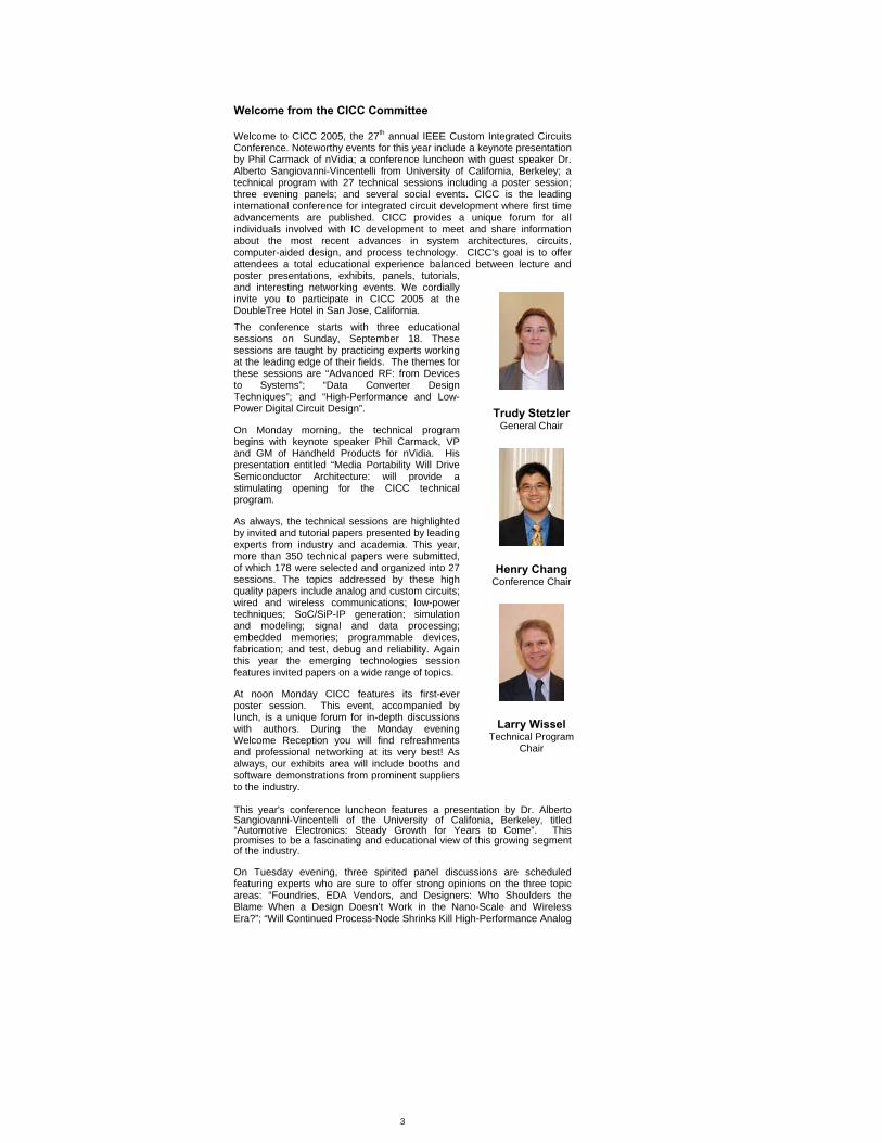
Trudy Stetzler General Chair
Henry Chang Conference Chair
Larry Wissel Technical Program
Chair
Welcome from the CICC Committee Welcome to CICC 2005, the 27th annual IEEE Custom Integrated Circuits Conference. Noteworthy events for this year include a keynote presentation by Phil Carmack of nVidia; a conference luncheon with guest speaker Dr. Alberto Sangiovanni-Vincentelli from University of California, Berkeley; a technical program with 27 technical sessions including a poster session; three evening panels; and several social events. CICC is the leading international conference for integrated circuit development where first time advancements are published. CICC provides a unique forum for all individuals involved with IC development to meet and share information about the most recent advances in system architectures, circuits, computer-aided design, and process technology. CICC's goal is to offer attendees a total educational experience balanced between lecture and poster presentations, exhibits, panels, tutorials, and interesting networking events. We cordially invite you to participate in CICC 2005 at the DoubleTree Hotel in San Jose, California.
The conference starts with three educational sessions on Sunday, September 18. These sessions are taught by practicing experts working at the leading edge of their fields. The themes for these sessions are “Advanced RF: from Devices to Systems”; “Data Converter Design Techniques”; and “High-Performance and Low-Power Digital Circuit Design”. On Monday morning, the technical program begins with keynote speaker Phil Carmack, VP and GM of Handheld Products for nVidia. His presentation entitled “Media Portability Will Drive Semiconductor Architecture: will provide a stimulating opening for the CICC technical program. As always, the technical sessions are highlighted by invited and tutorial papers presented by leading experts from industry and academia. This year, more than 350 technical papers were submitted, of which 178 were selected and organized into 27 sessions. The topics addressed by these high quality papers include analog and custom circuits; wired and wireless communications; low-power techniques; SoC/SiP-IP generation; simulation and modeling; signal and data processing; embedded memories; programmable devices, fabrication; and test, debug and reliability. Again this year the emerging technologies session features invited papers on a wide range of topics. At noon Monday CICC features its first-ever poster session. This event, accompanied by lunch, is a unique forum for in-depth discussions with authors. During the Monday evening Welcome Reception you will find refreshments and professional networking at its very best! As always, our exhibits area will include booths and software demonstrations from prominent suppliers to the industry. This year's conference luncheon features a presentation by Dr. Alberto Sangiovanni-Vincentelli of the University of Califonia, Berkeley, titled “Automotive Electronics: Steady Growth for Years to Come”. This promises to be a fascinating and educational view of this growing segment of the industry. On Tuesday evening, three spirited panel discussions are scheduled featuring experts who are sure to offer strong opinions on the three topic areas: “Foundries, EDA Vendors, and Designers: Who Shoulders the Blame When a Design Doesn’t Work in the Nano-Scale and Wireless Era?”; “Will Continued Process-Node Shrinks Kill High-Performance Analog

4
Design?”; and “Analog Behavioral Modeling: Fantasy, Fad, or Foundation for the Future?” This year the CICC is co-locating with the IEEE Behavior, Modeling, and Simulation Conference 2005. BMAS will take place September 22 – 23 at the DoubleTree Hotel, San Jose, California. Visit the BMAS website at www.bmas-conf.org for complete conference information. We extend our thanks to all the authors who spent many hours on the preparation of their submitted papers. We also wish to thank the CICC Technical Program Committee and our dedicated conference staff for all of their hard work and support. Their diligent efforts keep CICC as the best place to discover the latest in integrated circuit innovations, to hear the newest product announcements, and to debate the most effective business strategies. See you in San Jose!
Visit our website at www.ieee-cicc.org IEEE CICC is sponsored by:
The Institute of Electrical and Electronic Engineers
The IEEE Solid-State Circuits
Society
Technically co-sponsored by the Electron Devices
Society
5
EDUCATIONAL SESSIONS
Chairperson: David Allee, Arizona State University
Ed. Session 1 – Data Converter Design Techniques Oak Ballroom, Sunday, September 18
Organizer: Eric Naviasky, Cadence Design Systems, Inc Co-Organizer: Un-Ku Moon, Oregon State University 8:00 – 9:50 E1-1
Design Techniques for High Speed Data Converters William Evans, Cadence Design Systems
New ultra-wideband communications architectures will require ADCs with number of bits and sample rates previously associated with specialized applications such as digital oscilloscopes and radar receivers. Companion DACs with sample rates in excess of 1 GHz will also be required. These new converters, however, must be low in both power and area and must be integrated into large SoCs to reduce the total system cost for consumer electronics applications. We will discuss the advantages and disadvantages of different high-speed data converter architectures and then discuss different simulation techniques to aid in the design of key converter building blocks such as sample and holds and comparators. A brief case study of a low-power 6-bit 1 GHz ADC design will be presented. The special challenges of integrating these ADCs into large SoCs will be discussed and different ADC test techniques suitable for high-speed data converters will be presented. 10:10 – 12:00 E1-2 Understanding Delta-Sigma Data Converters
Richard Schreier, Analog Devices Following the book with the same title, this tutorial introduces the most important concepts underlying delta-sigma ADCs and DACs. The properties of inherent linearity and inherent anti-aliasing are explained in the context of the first-order modulator (MOD1). The second-order modulator (MOD2) is derived recursively from MOD1, and both MOD1 and MOD2 are used to illustrate the phenomena of idle-channel noise and tones. A general structure capable of describing arbitrary-order modulators is given, and the high-level design of a high-order modulator with the Delta-Sigma Toolbox is demonstrated. Bandpass, quadrature and cascade modulators are explained using the same theoretical framework. The tutorial concludes with a catalog of useful delta-sigma tricks and building blocks. 1:00 – 2:50 E1-3 Variability, a Barrier to Further CMOS Scaling
Marcel. J.M. Pelgrom (presenting), Philips Hans P. Tuinhout, Harry J.M Veendrick , Philips
Circuit operation depends on the ability to control and reproduce transistor and process parameters such as oxide thickness, dielectric constants, doping levels, width and length. Variation in processing was in the past countered by defining process corners: boundaries in parameter variation that accounted for remaining process tolerances. With the improved control over processing, this batch-to-batch variation is largely under control.
6
However, now a new class of phenomena has appeared: the intra-die variability. In conventional ICs, analog circuits with a differential operation (such as analog-to-digital converters) were already affected by this parameter spread. The remaining variation between otherwise identical components is generally described by “mismatch” parameters. Along with this mechanical and electrical stress, local operating condition variations such as voltage and temperature and interference (supply and substrate noise, cross-talk, etc.) are of major importance to optimize circuit performance. For a long time, digital designers did not consider this intra-die variability. However, due to scaling, the margins in digital designs reduce. Also the effective number of atoms, involved in the local definition of electrical parameters is also reduced, thereby increasing the local variability to a level where even the classical full-swing noise margins in digital circuits are affected. Where analog designers have to option to increase area or implement correction circuits, digital designers have to cope differently with these effects. The tutorial will focus on mechanisms which originate from physical, electrical, thermal and interference effects causing intra-die variations. In particularly the effects of jitter, mismatch and substrate noise in digital circuits will be considered. 3:10 – 5:00 E1-4 High-Performance Pipelined ADCs
Ian Galton, University of California, San Diego This lecture presents an introduction to pipelined ADCs and digital background calibration techniques to mitigate the effects of non-ideal circuit behavior. First, the system-level concepts underlying pipelined ADCs are presented in terms of a particular pipelined ADC example, including sensitivity to non-ideal behavior of the various pipeline components. It is shown that pipelined ADCs are highly sensitive to interstage gain errors and mismatches among certain components, especially when designed for low supply voltages. Digital calibration techniques that address these problems are then presented. The system-level concepts and circuit-level implementation issues are presented in the context of a 1.8 V CMOS pipelined ADC design example wherein the techniques are shown to enable state-of-the-art performance.
Ed. Session 2 – Advanced RF: From Devices to Systems Fir Ballroom, Sunday, September 18
Organizer: Kris Iniewski, University of Alberta Co-Organizer: Kathleen Philips, Philips Research 8:00 – 9:50 E2-1 RF 101: An Introduction to RF Wireless Circuits and
Systems Dr. James Haslett, ATIPS, University of Calgary
Analog wireless RF integrated circuit research and development has seen a dramatic change over the past 5 - 10 years, and the techniques involved in designing conventional heterodyne and homodyne transceiver systems are rapidly maturing. As minimum feature sizes decrease in various technologies, system capability has continued to improve, along with bottlenecks to complete monolithic radio integration limited by poor quality on-chip passives, and by linearity, noise and other issues. RF filters and high-linearity low-voltage integrated power amplifiers represent major hurdles to be
7
overcome. The quest to fully integrate high-performance radios in CMOS technologies continues unabated, because of the resulting ability to realize substantial DSP capability in the same processes. New approaches that move the digital part of the radio toward the LNA are being investigated. However, as minimum feature sizes and power-supply voltages continue to decrease, we may be reaching a turning point in analog RF IC design that will prevent further improvements in fully monolithic designs. This lecture will review the key issues involved in designing transceivers for wireless applications, beginning with electrical and noise modeling issues and associated CAD tool deficiencies. Figures of merit for fabrication processes and passive components will be described. The basic transceiver building blocks (LNAs, Mixers, VCOs and PLLs) will be reviewed. Non-ideal behavior in terms of compression, intermodulation distortion and noise will be discussed and key performance issues associated with various modulation schemes will be examined. Major hurdles to be addressed in the future, such as substrate noise coupling in mixed-signal IC's, linearity issues associated with low-power supply voltages, techniques for realizing high-quality passives, and new transmission schemes will be discussed briefly, as a lead-in to the remaining topics in the education session. 10:10 – 12:00 E2-2 RF System in Package Integration
Dr. Freek E. van Straten, Philips Semiconductors, Innovation Center RF
Today, the RF functionality of many handheld devices is rapidly becoming a commodity resulting in a ongoing size and cost reduction. Passive integration technologies and System in Package (SiP) integration are the key enablers for this. The presentation will concentrate on RF (sub) System integration and SiP. Since passive components play an important role in the realization of RF applications the talk will start by explaining those components and typical implementation examples based on different technologies. Inductors are often required but turn out to be difficult to implement since they do not really scale vs technology and often have high losses. A balun function consisting of inductive components will be taken as example and is a good carrier to demonstrate passive integration. In the second part, the aim is to work out more (state of the art) examples. LTCC technology offers a good basis for low capacitor and inductor integration and can simultaneously act as substrate for other components. Standard laminate PCB can not only be used for interconnect but yield good inductors at low cost and can also be used for baluns. As new technology, thin film components on High Resistivity Silicon (HRS) will be shown as the integration basis for transceiver applications. 1:00 – 2:50 E2-3 Circuit Design for Ultra-Wide Band (UWB)
Dr. Domine Leenaerts, Philips Semiconductors Since the FCC opened up the spectrum for Ultra Wide Band (UWB) operation in the 3.1 to 10.6GHz range, several standards have been proposed to realize high-rate short-range communication systems. The multi-band OFDM alliance proposal divides the spectrum into QPSK-OFDM modulated sub-bands of 528MHz. The mandatory mode of operation implements a frequency-hopping scheme in the three lower bands from 3.1GHz to 4.8GHz with a transmit power below the FCC limit of – 41.25dBm/MHz. These low signal levels
8
require a low-noise receive chain, while the presence of strong out-of-band interferers in the 2.4 and 5GHz bands and the need for co-existence with systems operating in these bands mandate a high linearity and selectivity to achieve robust high-rate data transmission. A frequency-hopping scheme is applied to achieve efficient and robust communication for piconets operating simultaneously in close proximity. This scheme employs hopping between the carrier frequencies of the lower three bands at 3432MHz, 3960MHz, and 4488MHz, with a period of 312.5ns. The frequency synthesizer switches between the carrier frequencies within a maximum transition time of 9ns. The demands on the purity of the generated carriers are also very stringent: all spurious tones in the 5GHz range must be below -50dBc to avoid down-conversion of strong out-of-band interferers into the wanted channels. The presentation will briefly discuss the system aspects of UWB communication and will discuss in more detail the design aspects of needed circuitry to build up an UWB radio transceiver, keeping in mind the afore mentioned design requirements. 3:10 – 5:00 E2-4 RF Design Tools for Technology Trade-Offs
Dr. Piet Wambacq, IMEC Modern RF systems are mixed-signal by nature: several signal impairments caused by the analog circuits can be corrected by digital circuitry, which in future downscaled CMOS technologies consume area and energy that are small compared to the area and energy consumption of analog blocks. However, digital systems become increasingly more complex, and the digital switching noise that they produce becomes a more and more important source of crosstalk to the analog circuitry, causing malfunctioning of the latter. There is an increasing pressure on the few analog circuits that remain in a radio: higher data rates need to be transmitted and received by the radio while the energy consumption of the latter must decrease. Can new technologies make the analog circuits for these radios? In other words, will downscaling be beneficial to design the radio part of future wireless systems? This lecture will address these questions by comparing different circuits implemented in different CMOS technologies, hereby using different technology generations and different types of passive components (such as, using standard metal layers or above-IC processing). These technology trade-offs are investigated based on measured circuit performance as well as on an approach that allows for a quick assessment of performance and power consumption of a given circuit topology as a function of technology. Furthermore, the problem of crosstalk from digital to analog through the semiconducting substrate is addressed with an accurate approach to predict and model, prior to processing, the substrate noise generation, propagation and resulting analog and RF performance degradation. This approach should allow for an understanding of the mechanisms of substrate-noise impact and for an accurate prediction of noise suppression by isolation techniques.

9
Ed. Session 3 – High-Performance and Low-Power Digital Circuit Design
Pine Ballroom, Sunday, September 18 Organizer: Tom Andre, Freescale Semiconductors 8:00 – 9:50 E3-1 Circuit Design for Low Power and High Performance
Lawrence T. Clark, Arizona State University The tutorial covers state-of-the-art techniques for minimizing standby and active power in high-performance digital circuits. The tutorial begins with the impact of transistor scaling on transistor leakage and design techniques to address the resulting standby power. Circuits and results from applying reverse body bias, as well as the use of shadow latches, which may be more effective in sub-100nm technologies, will be discussed. The application and the efficacy of low-power modes, their power penalties, latencies, and limitations will be discussed. The tutorial will then discuss design techniques for limiting active (circuit-switching) power. Practical application of voltage scaling, dynamic voltage scaling, and circuit limitations to low voltage operation, such as SRAM VDD(min), will be reviewed. Various techniques to reduce power in memories and other dynamic circuits will be reviewed, with examples from high-performance micro-processor memory and register file blocks. The power impact of architecture and micro-architectural choices will also be discussed. The tutorial will conclude with a summary of the proposed techniques, their relative benefit vs. design difficulty and prospects for future low-power ICs. 10:10 – 12:00 E3-2 Leakage- and Variation-Tolerant High-Performance
Circuit Technologies for Sub-45nm CMOS Ram Krishnamurthy, Intel Corporation
As traditional CMOS technology scaling becomes difficult beyond 65nm node, new challenges arise for achieving high performance at low power under aggravated transistor leakage and parameter variations. In this tutorial, we discuss some of the primary sub-45nm CMOS leakage mechanisms and variations, related scaling challenges and outline some of the new paradigm shifts necessary to overcome these barriers. Leakage- and variation-tolerant design technologies are presented to combat these challenges, including on-die leakage sensing and compensation techniques; dynamic, pseudo-static and fully-static circuit technologies for large signal caches and register file arrays; and energy-efficient leakage/variation-tolerant design methodologies. Many chip design examples illustrating these technologies are reviewed. 1:00 – 2:50 E3-3 Low-Power Memory Design for 65nm
Sreedhar Natarajan, Emerging Memory Technologies The semiconductor industry is facing a bottleneck with many unresolved issues in process and design at the 90nm node and below. Technology scaling and consumer demand for portable applications is forcing memory designers and process engineers to come up with innovative techniques to achieve low power in any memory technology With a rising trend of SOC die area (as high as 70%) devoted to memory, design techniques for lowering active and standby power in memories are becoming more critical to overall system power
10
reduction. Introduction of new techniques either through process or design are essential to combat the scalability issues at 90nm and below. In addition to power requirements at 90nm and 65nm, which are the most dominant in the industry today, soft error rates are equally a predominant factor affecting the functionality of memory cells and circuits. This tutorial will very briefly outline the leakage mechanisms and solutions for RAM designs, followed by description of the soft error sensitivity of memories and logic. Logic SER may be as significant as SRAM SER and is only getting worse at smaller geometries. Design and process issues that affect yield will also be discussed as part of a brief introduction to design for manufacturability (DFM) following with a brief outline into DFT techniques. 3:10 – 5:00 E3-4 Circuit Design Techniques in SOI
Andrew Marshall, Texas Instruments Inc. Silicon-on-insulator (SOI) technology has evolved into an important frontier in the development of low-power and high-performance circuit design. FinFET and multi-gate SOI have recently become areas of intense scrutiny, and circuits are being designed with these structures. FinFET and multi-gate SOI are inherently simpler to design than the previous generations of SOI, while still offering performance improvement, reduced power, component isolation and an increase in circuit density compared to previously developed SOI techniques such as partially depleted and fully depleted SOI. A brief history and overview of the major SOI process options is given and a comparison is made between SOI and bulk material. The various types of SOI are discussed, especially FinFET, multi-gate, partially and fully depleted structures. Tradeoffs are considered, including leakage effects, thermal issues, transistor matching and the history and kink effects observed in some SOI technologies. The challenge of modeling SOI devices is explored and some concepts for successful SOI circuit layout are introduced, including a discussion of various options for the reduction of thermal self-heating effects. The development of circuits for low voltage and low power are discussed for analog and digital applications. In conclusion, trends in SOI development are addressed.
EXHIBITS CICC once again combines its outstanding technical program with a variety of exhibitors. Exhibits will include displays and demonstrations by semiconductor manufacturers, software tool suppliers, design service houses, and leading electronics industry publications. The Exhibit Hall will be the site for Monday's Welcome Reception and Tuesday evening's Happy Hour. Donner Pass Ballroom Monday, September 19 3:00 pm - 8:00 pm – Exhibits Open 5:30 pm - 8:00 pm Welcome Reception Tuesday, Septebmer 20 3:00 pm - 7:00 pm – Exhibits Open 5:30 pm - 7:00 pm Happy Hour
11
TECHNICAL SESSIONS
Monday, September 19 – Wednesday, September 21
Session 1 – Keynote Presentation Oak Ballroom, Monday Morning, September 19
8:00 am Welcome/Opening Remarks
Awards Presentations Keynote Speaker Introduction Trudy Stetzler, General Chair
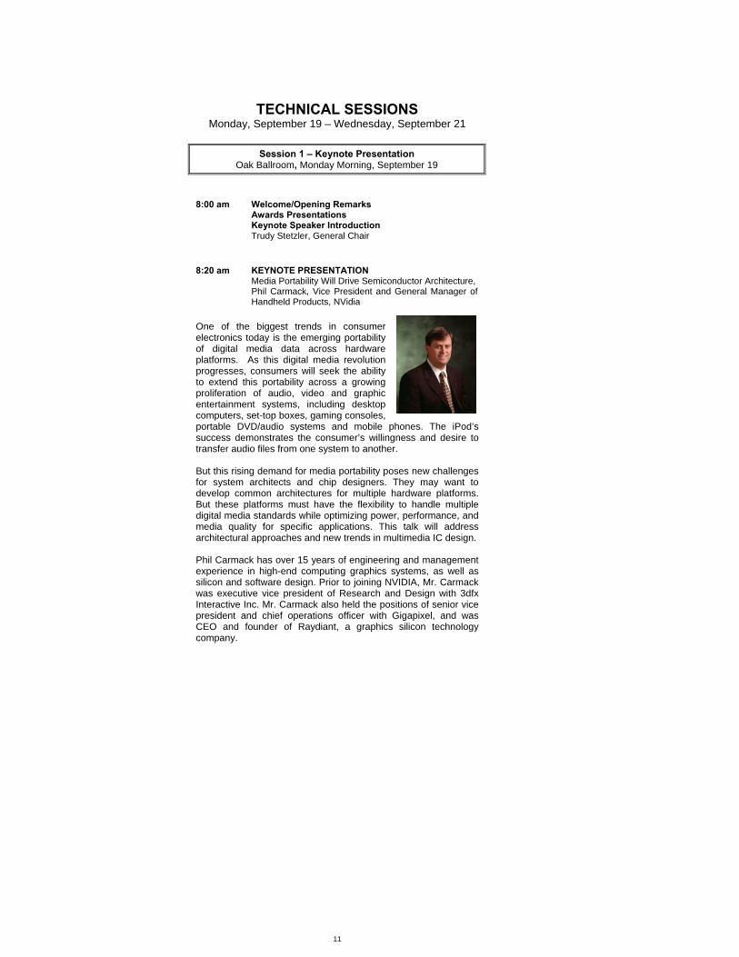
8:20 am KEYNOTE PRESENTATION
Media Portability Will Drive Semiconductor Architecture, Phil Carmack, Vice President and General Manager of Handheld Products, NVidia
One of the biggest trends in consumer electronics today is the emerging portability of digital media data across hardware platforms. As this digital media revolution progresses, consumers will seek the ability to extend this portability across a growing proliferation of audio, video and graphic entertainment systems, including desktop computers, set-top boxes, gaming consoles, portable DVD/audio systems and mobile phones. The iPod’s success demonstrates the consumer’s willingness and desire to transfer audio files from one system to another. But this rising demand for media portability poses new challenges for system architects and chip designers. They may want to develop common architectures for multiple hardware platforms. But these platforms must have the flexibility to handle multiple digital media standards while optimizing power, performance, and media quality for specific applications. This talk will address architectural approaches and new trends in multimedia IC design. Phil Carmack has over 15 years of engineering and management experience in high-end computing graphics systems, as well as silicon and software design. Prior to joining NVIDIA, Mr. Carmack was executive vice president of Research and Design with 3dfx Interactive Inc. Mr. Carmack also held the positions of senior vice president and chief operations officer with Gigapixel, and was CEO and founder of Raydiant, a graphics silicon technology company.
12
Session 2 – Body Wellness Without Wires Oak Ballroom, Monday Morning, September 19
Chair: Jim Lipman Co-Chair: Albert Wang
Silicon meets flesh and blood! These invited papers discuss how wireless technology is impacting information processing for smart medical microsystems and body area networks. 10:00 am Introduction 10:05 am 2-1
Wirelessly Powered and Bidirectionally Data Exchanged in Smart Medical Microsystems (INVITED), M. Sawan, Y. Hu and J. Coulombe, Ecole Polytechnique de Montreal, Montreal, Quebec, Canada
10:55 am 2-2
Human++: Autonomous Wireless Sensors for Body Area Networks (INVITED), B. Gyselinckx, C. Van Hoof, J. Ryckaert, R. Yazicioglu, P. Fiorini and V. Leonov, IMEC, Leuven, Belgium
Session 3 – Noise and Reliability Containment Approaches Fir Ballroom, Monday Morning, September 19
Chair: Gordon Roberts Co-Chair: Robert Aitken This session begins with a tutorial overview of the “Design For” platform in sub-65nm technologies and is followed by three papers related to on-chip noise measurement and containment. 10:00 am Introduction 10:05 am 3-1
Robust Platform Design in Advanced VLSI Technologies (INVITED), D. Leavins, K.S. Kim, S. Mitra and E. Rodriguez, Intel Corporation, Folsom, CA
10:55 am 3-2
An Integrated Timing and Dynamic Supply Noise Verification for Nano-meter CMOS SoC Designs, K. Shimazaki, M. Fukazawa*, M. Nagata*, S. Miyahara, M. Hirata, K. Sato, and H. Tsujikawa, Matsushita Electrical Industrial Co., Ltd., Nagaokakyo, Japan, *Kobe University, Kobe, Japan
11:20 am 3-3
Substrate-Noise and Random-Fluctuations Reduction with Self-Adjusted Forward Body Bias, Y. Komatsu, K. Ishibashi, M. Yamamoto, T. Tsukada, K. Shimazaki*, M. Fukazawa* and M. Nagata*, Semiconductor Technology Academic Research Center (STARC), Yokohama, Japan, *Kobe University, Kobe, Japan
11:45 am 3-4
Auto-Referenced On-Die Power Supply Noise Measurement Circuit, C. Chansungsan, Intel Corporation, Hillsboro, OR
13
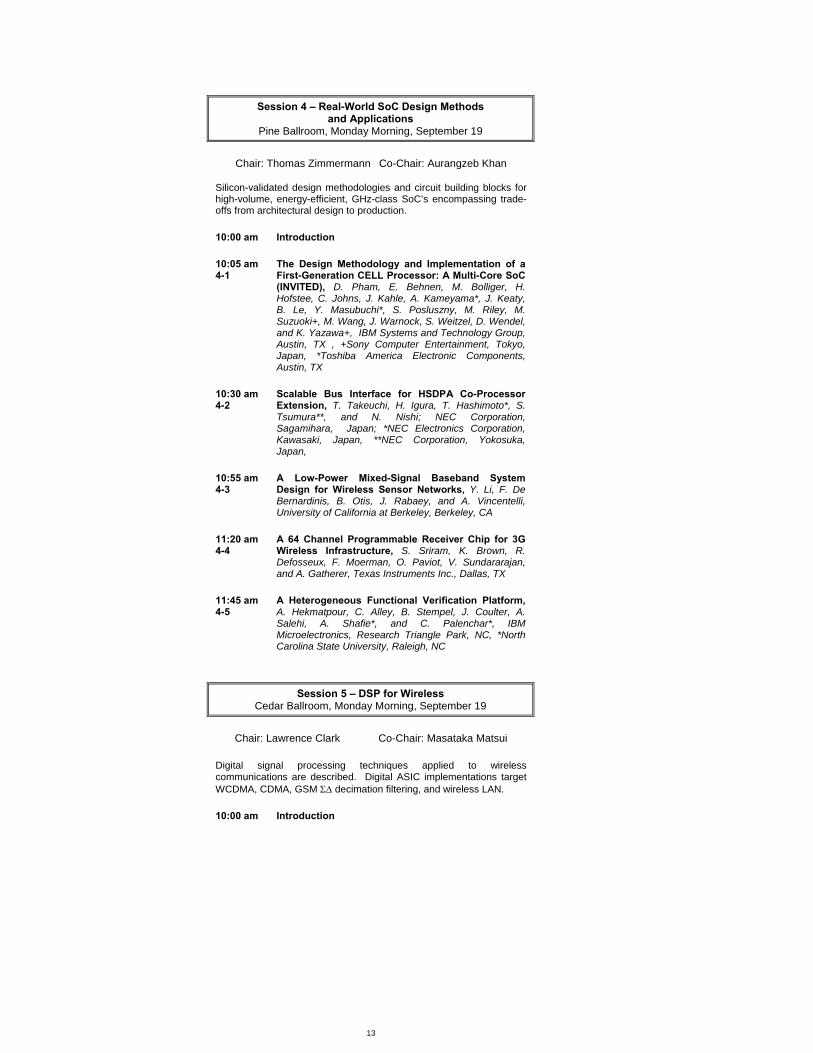
Session 4 – Real-World SoC Design Methods and Applications
Pine Ballroom, Monday Morning, September 19
Chair: Thomas Zimmermann Co-Chair: Aurangzeb Khan Silicon-validated design methodologies and circuit building blocks for high-volume, energy-efficient, GHz-class SoC’s encompassing trade-offs from architectural design to production. 10:00 am Introduction 10:05 am 4-1
The Design Methodology and Implementation of a First-Generation CELL Processor: A Multi-Core SoC (INVITED), D. Pham, E. Behnen, M. Bolliger, H. Hofstee, C. Johns, J. Kahle, A. Kameyama*, J. Keaty, B. Le, Y. Masubuchi*, S. Posluszny, M. Riley, M. Suzuoki+, M. Wang, J. Warnock, S. Weitzel, D. Wendel, and K. Yazawa+, IBM Systems and Technology Group, Austin, TX , +Sony Computer Entertainment, Tokyo, Japan, *Toshiba America Electronic Components, Austin, TX
10:30 am 4-2
Scalable Bus Interface for HSDPA Co-Processor Extension, T. Takeuchi, H. Igura, T. Hashimoto*, S. Tsumura**, and N. Nishi; NEC Corporation, Sagamihara, Japan; *NEC Electronics Corporation, Kawasaki, Japan, **NEC Corporation, Yokosuka, Japan,
10:55 am 4-3
A Low-Power Mixed-Signal Baseband System Design for Wireless Sensor Networks, Y. Li, F. De Bernardinis, B. Otis, J. Rabaey, and A. Vincentelli, University of California at Berkeley, Berkeley, CA
11:20 am 4-4
A 64 Channel Programmable Receiver Chip for 3G Wireless Infrastructure, S. Sriram, K. Brown, R. Defosseux, F. Moerman, O. Paviot, V. Sundararajan, and A. Gatherer, Texas Instruments Inc., Dallas, TX
11:45 am 4-5
A Heterogeneous Functional Verification Platform, A. Hekmatpour, C. Alley, B. Stempel, J. Coulter, A. Salehi, A. Shafie*, and C. Palenchar*, IBM Microelectronics, Research Triangle Park, NC, *North Carolina State University, Raleigh, NC
Session 5 – DSP for Wireless Cedar Ballroom, Monday Morning, September 19
Chair: Lawrence Clark Co-Chair: Masataka Matsui
Digital signal processing techniques applied to wireless communications are described. Digital ASIC implementations target WCDMA, CDMA, GSM Σ∆ decimation filtering, and wireless LAN. 10:00 am Introduction
14
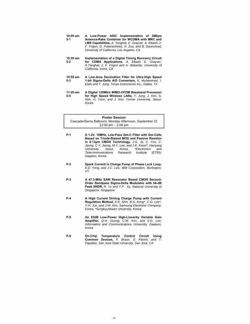
10:05 am 5-1
A Low-Power ASIC Implementation of 2Mbps Antenna-Rake Combiner for WCDMA with MRC and LMS Capabilities, A. Tarighat, E. Grayver, A. Eltawil, J-F. Frigon, G. Poberezhskiy, H. Zou, and B. Daneshrad, University of California, Los Angeles, CA
10:30 am 5-2
Implementation of a Digital Timing Recovery Circuit for CDMA Applications, A. Eltawil, E. Grayver, A.Tarighat, J. F. Frigon and A. Abbasfar, University of California, Irvine, CA
10:55 am 5-3
A Low-Area Decimation Filter for Ultra-High Speed 1-bit Sigma-Delta A/D Converters, K. Muhammad, I. Elahi and T. Jung, Texas Instruments Inc., Dallas, TX
11:20 am 5-4
A Digital 120Mb/s MIMO-OFDM Baseband Processor for High Speed Wireless LANs, Y. Jung, J. Kim, S. Noh, H. Yoon, and J. Kim, Yonsei University, Seoul, Korea
Poster Session Cascade/Sierra Ballroom, Monday Afternoon, September 21
12:00 pm – 2:00 pm P-1 A 1.2V, 10MHz, Low-Pass Gm-C Filter with Gm-Cells
Based on Triode-Biased MOS and Passive Resistor in 0.13µm CMOS Technology, J-G. Jo, C. Yoo, C. Jeong, C-Y. Jeong, M-Y. Lee, and J-K. Kwon*, Hanyang University, Seoul, Korea, *Electronics and Telecommunications Research Institute (ETRI), Daejeon, Korea
P-2 Spark Current in Charge Pump of Phase Lock Loop,
K.D. Feng and J.C. Lee, IBM Corporation, Burlington, VT
P-3 A 47.3-MHz SAW Resonator Based CMOS Second-
Order Bandpass Sigma-Delta Modulator with 54-dB Peak SNDR, R. Yu and Y.P. Xu, National University of Singapore, Singapore
P-4 A High Current Driving Charge Pump with Current
Regulation Method, S-K. Shin, B-S. Kong*, C-G. Lee*, Y-H. Jun, and J-W. Kim, Samsung Electronic Company, Korea, *Sungkyunkwan University, Korea,
P-5 An 83dB Low-Power High-Linearity Variable Gain
Amplifier, Q-H. Duong, C-W. Kim, and S-G. Lee, Information and Communications University, Daejeon, Korea
P-6 On-Chip Temperature Control Circuit Using
Common Devices, F. Braun, D. Parent, and T. Papalias, San Jose State Unversity, San Jose, CA
15
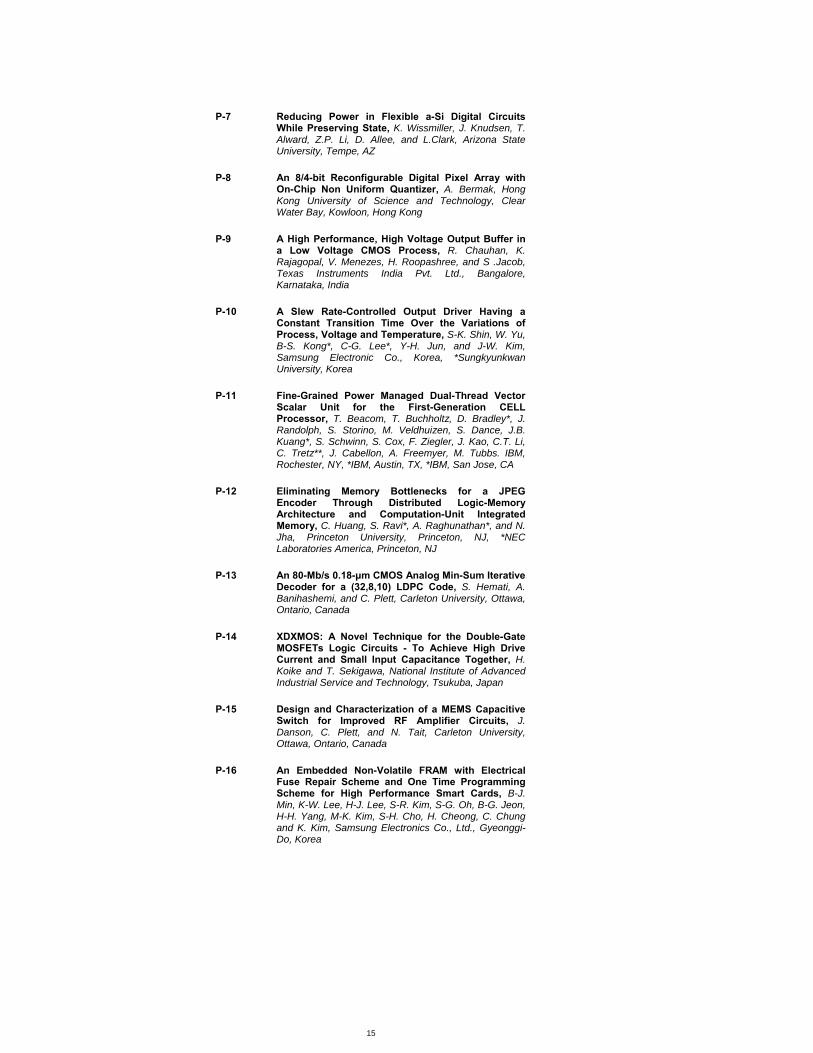
P-7 Reducing Power in Flexible a-Si Digital Circuits
While Preserving State, K. Wissmiller, J. Knudsen, T. Alward, Z.P. Li, D. Allee, and L.Clark, Arizona State University, Tempe, AZ
P-8 An 8/4-bit Reconfigurable Digital Pixel Array with
On-Chip Non Uniform Quantizer, A. Bermak, Hong Kong University of Science and Technology, Clear Water Bay, Kowloon, Hong Kong
P-9 A High Performance, High Voltage Output Buffer in
a Low Voltage CMOS Process, R. Chauhan, K. Rajagopal, V. Menezes, H. Roopashree, and S .Jacob, Texas Instruments India Pvt. Ltd., Bangalore, Karnataka, India
P-10 A Slew Rate-Controlled Output Driver Having a
Constant Transition Time Over the Variations of Process, Voltage and Temperature, S-K. Shin, W. Yu, B-S. Kong*, C-G. Lee*, Y-H. Jun, and J-W. Kim, Samsung Electronic Co., Korea, *Sungkyunkwan University, Korea
P-11 Fine-Grained Power Managed Dual-Thread Vector
Scalar Unit for the First-Generation CELL Processor, T. Beacom, T. Buchholtz, D. Bradley*, J. Randolph, S. Storino, M. Veldhuizen, S. Dance, J.B. Kuang*, S. Schwinn, S. Cox, F. Ziegler, J. Kao, C.T. Li, C. Tretz**, J. Cabellon, A. Freemyer, M. Tubbs. IBM, Rochester, NY, *IBM, Austin, TX, *IBM, San Jose, CA
P-12 Eliminating Memory Bottlenecks for a JPEG
Encoder Through Distributed Logic-Memory Architecture and Computation-Unit Integrated Memory, C. Huang, S. Ravi*, A. Raghunathan*, and N. Jha, Princeton University, Princeton, NJ, *NEC Laboratories America, Princeton, NJ
P-13 An 80-Mb/s 0.18-µm CMOS Analog Min-Sum Iterative
Decoder for a (32,8,10) LDPC Code, S. Hemati, A. Banihashemi, and C. Plett, Carleton University, Ottawa, Ontario, Canada
P-14 XDXMOS: A Novel Technique for the Double-Gate
MOSFETs Logic Circuits - To Achieve High Drive Current and Small Input Capacitance Together, H. Koike and T. Sekigawa, National Institute of Advanced Industrial Service and Technology, Tsukuba, Japan
P-15 Design and Characterization of a MEMS Capacitive
Switch for Improved RF Amplifier Circuits, J. Danson, C. Plett, and N. Tait, Carleton University, Ottawa, Ontario, Canada
P-16 An Embedded Non-Volatile FRAM with Electrical
Fuse Repair Scheme and One Time Programming Scheme for High Performance Smart Cards, B-J. Min, K-W. Lee, H-J. Lee, S-R. Kim, S-G. Oh, B-G. Jeon, H-H. Yang, M-K. Kim, S-H. Cho, H. Cheong, C. Chung and K. Kim, Samsung Electronics Co., Ltd., Gyeonggi-Do, Korea
16
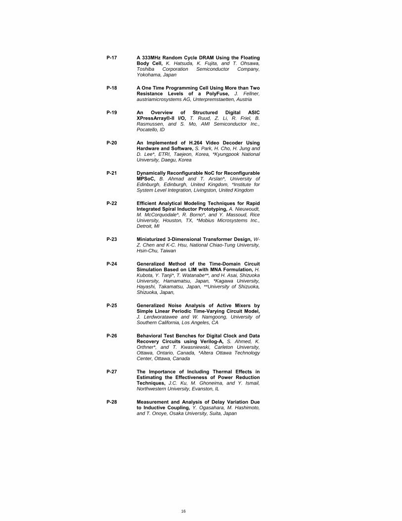
P-17 A 333MHz Random Cycle DRAM Using the Floating
Body Cell, K. Hatsuda, K. Fujita, and T. Ohsawa, Toshiba Corporation Semiconductor Company, Yokohama, Japan
P-18 A One Time Programming Cell Using More than Two
Resistance Levels of a PolyFuse, J. Fellner, austriamicrosystems AG, Unterpremstaetten, Austria
P-19 An Overview of Structured Digital ASIC
XPressArray®-II I/O, T. Ruud, Z. Li, R. Friel, B. Rasmussen, and S. Mo, AMI Semiconductor Inc., Pocatello, ID
P-20 An Implemented of H.264 Video Decoder Using
Hardware and Software, S. Park, H. Cho, H. Jung and D. Lee*, ETRI, Taejeon, Korea, *Kyungpook National University, Daegu, Korea
P-21 Dynamically Reconfigurable NoC for Reconfigurable
MPSoC, B. Ahmad and T. Arslan*, University of Edinburgh, Edinburgh, United Kingdom, *Institute for System Level Integration, Livingston, United Kingdom
P-22 Efficient Analytical Modeling Techniques for Rapid
Integrated Spiral Inductor Prototyping, A. Nieuwoudt, M. McCorquodale*, R. Borno*, and Y. Massoud, Rice University, Houston, TX, *Mobius Microsystems Inc., Detroit, MI
P-23 Miniaturized 3-Dimensional Transformer Design, W-
Z. Chen and K-C. Hsu, National Chiao-Tung University, Hsin-Chu, Taiwan
P-24 Generalized Method of the Time-Domain Circuit
Simulation Based on LIM with MNA Formulation, H. Kubota, Y. Tanji*, T. Watanabe**, and H. Asai, Shizuoka University, Hamamatsu, Japan, *Kagawa University, Hayashi, Takamatsu, Japan, **University of Shizuoka, Shizuoka, Japan,
P-25 Generalized Noise Analysis of Active Mixers by
Simple Linear Periodic Time-Varying Circuit Model, J. Lerdworatawee and W. Namgoong, University of Southern California, Los Angeles, CA
P-26 Behavioral Test Benches for Digital Clock and Data
Recovery Circuits using Verilog-A, S. Ahmed, K. Orthner*, and T. Kwasniewski, Carleton University, Ottawa, Ontario, Canada, *Altera Ottawa Technology Center, Ottawa, Canada
P-27 The Importance of Including Thermal Effects in
Estimating the Effectiveness of Power Reduction Techniques, J.C. Ku, M. Ghoneima, and Y. Ismail, Northwestern University, Evanston, IL
P-28 Measurement and Analysis of Delay Variation Due
to Inductive Coupling, Y. Ogasahara, M. Hashimoto, and T. Onoye, Osaka University, Suita, Japan
17
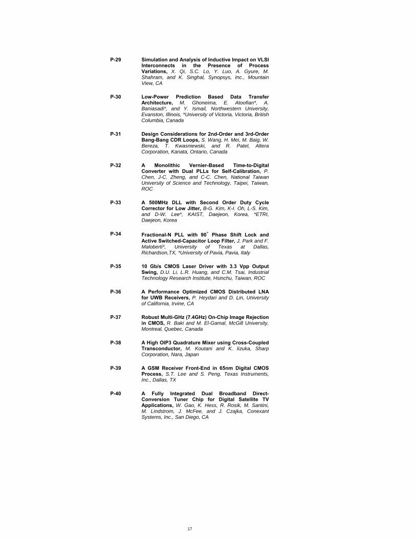
P-29 Simulation and Analysis of Inductive Impact on VLSI
Interconnects in the Presence of Process Variations, X. Qi, S.C. Lo, Y. Luo, A. Gyure, M. Shahram, and K. Singhal, Synopsys, Inc., Mountain View, CA
P-30 Low-Power Prediction Based Data Transfer
Architecture, M. Ghoneima, E. Atoofian*, A. Baniasadi*, and Y. Ismail, Northwestern University, Evanston, Illinois, *University of Victoria, Victoria, British Columbia, Canada
P-31 Design Considerations for 2nd-Order and 3rd-Order
Bang-Bang CDR Loops, S. Wang, H. Mei, M. Baig, W. Bereza, T. Kwasniewski, and R. Patel, Altera Corporation, Kanata, Ontario, Canada
P-32 A Monolithic Vernier-Based Time-to-Digital
Converter with Dual PLLs for Self-Calibration, P. Chen, J-C. Zheng, and C-C. Chen, National Taiwan University of Science and Technology, Taipei, Taiwan, ROC
P-33 A 500MHz DLL with Second Order Duty Cycle
Corrector for Low Jitter, B-G. Kim, K-I. Oh, L-S. Kim, and D-W. Lee*, KAIST, Daejeon, Korea, *ETRI, Daejeon, Korea
P-34 Fractional-N PLL with 90˚ Phase Shift Lock and
Active Switched-Capacitor Loop Filter, J. Park and F. Maloberti*, University of Texas at Dallas, Richardson,TX, *University of Pavia, Pavia, Italy
P-35 10 Gb/s CMOS Laser Driver with 3.3 Vpp Output
Swing, D.U. Li, L.R. Huang, and C.M. Tsai, Industrial Technology Research Institute, Hsinchu, Taiwan, ROC
P-36 A Performance Optimized CMOS Distributed LNA
for UWB Receivers, P. Heydari and D. Lin, University of California, Irvine, CA
P-37 Robust Multi-GHz (7.4GHz) On-Chip Image Rejection
in CMOS, R. Baki and M. El-Gamal, McGill University, Montreal, Quebec, Canada
P-38 A High OIP3 Quadrature Mixer using Cross-Coupled
Transconductor, M. Koutani and K. Iizuka, Sharp Corporation, Nara, Japan
P-39 A GSM Receiver Front-End in 65nm Digital CMOS
Process, S.T. Lee and S. Peng, Texas Instruments, Inc., Dallas, TX
P-40 A Fully Integrated Dual Broadband Direct-
Conversion Tuner Chip for Digital Satellite TV Applications, W. Gao, K. Hess, R. Rosik, M. Santini, M. Lindstrom, J. McFee, and J. Czajka, Conexant Systems, Inc., San Diego, CA
18
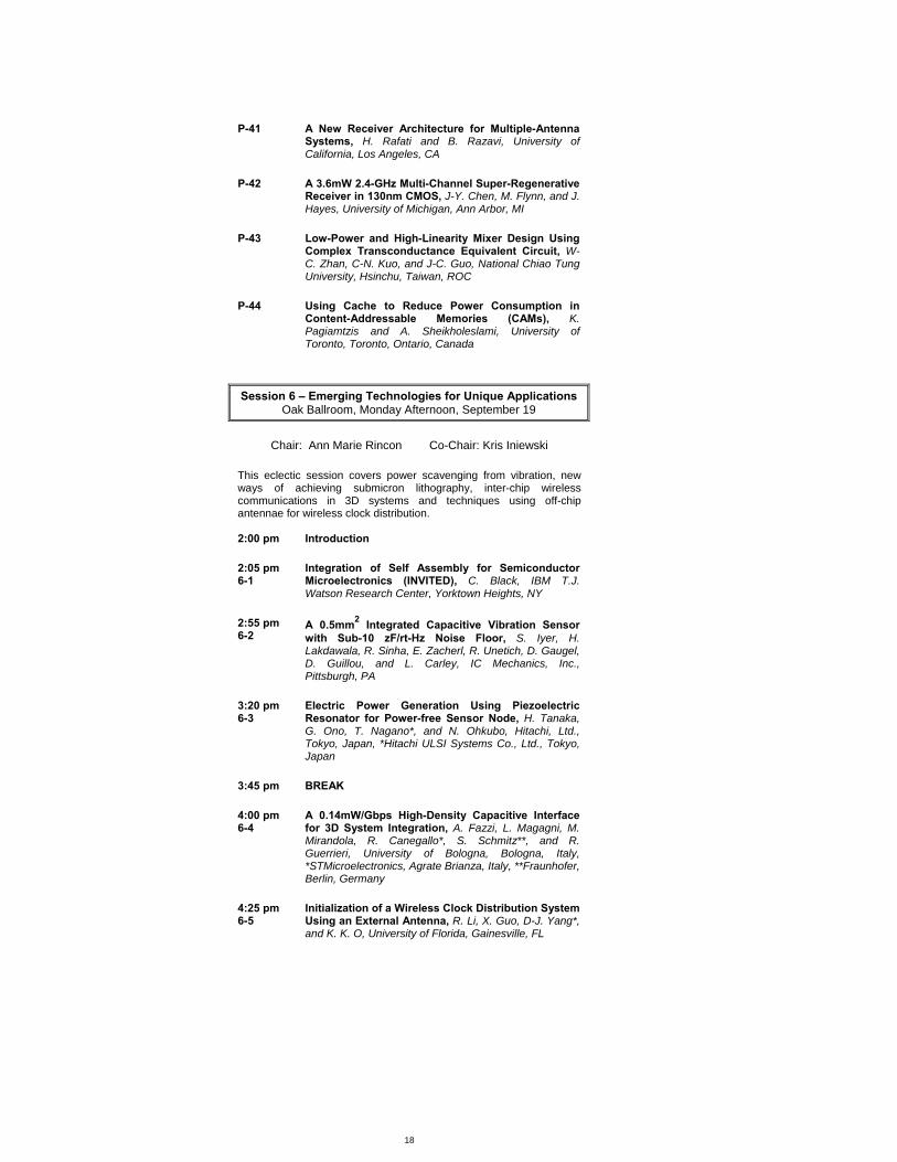
P-41 A New Receiver Architecture for Multiple-Antenna
Systems, H. Rafati and B. Razavi, University of California, Los Angeles, CA
P-42 A 3.6mW 2.4-GHz Multi-Channel Super-Regenerative
Receiver in 130nm CMOS, J-Y. Chen, M. Flynn, and J. Hayes, University of Michigan, Ann Arbor, MI
P-43 Low-Power and High-Linearity Mixer Design Using
Complex Transconductance Equivalent Circuit, W-C. Zhan, C-N. Kuo, and J-C. Guo, National Chiao Tung University, Hsinchu, Taiwan, ROC
P-44 Using Cache to Reduce Power Consumption in
Content-Addressable Memories (CAMs), K. Pagiamtzis and A. Sheikholeslami, University of Toronto, Toronto, Ontario, Canada
Session 6 – Emerging Technologies for Unique Applications
Oak Ballroom, Monday Afternoon, September 19
Chair: Ann Marie Rincon Co-Chair: Kris Iniewski This eclectic session covers power scavenging from vibration, new ways of achieving submicron lithography, inter-chip wireless communications in 3D systems and techniques using off-chip antennae for wireless clock distribution. 2:00 pm Introduction 2:05 pm 6-1
Integration of Self Assembly for Semiconductor Microelectronics (INVITED), C. Black, IBM T.J. Watson Research Center, Yorktown Heights, NY
2:55 pm 6-2
A 0.5mm2 Integrated Capacitive Vibration Sensor with Sub-10 zF/rt-Hz Noise Floor, S. Iyer, H. Lakdawala, R. Sinha, E. Zacherl, R. Unetich, D. Gaugel, D. Guillou, and L. Carley, IC Mechanics, Inc., Pittsburgh, PA
3:20 pm 6-3
Electric Power Generation Using Piezoelectric Resonator for Power-free Sensor Node, H. Tanaka, G. Ono, T. Nagano*, and N. Ohkubo, Hitachi, Ltd., Tokyo, Japan, *Hitachi ULSI Systems Co., Ltd., Tokyo, Japan
3:45 pm BREAK 4:00 pm 6-4
A 0.14mW/Gbps High-Density Capacitive Interface for 3D System Integration, A. Fazzi, L. Magagni, M. Mirandola, R. Canegallo*, S. Schmitz**, and R. Guerrieri, University of Bologna, Bologna, Italy, *STMicroelectronics, Agrate Brianza, Italy, **Fraunhofer, Berlin, Germany
4:25 pm 6-5
Initialization of a Wireless Clock Distribution System Using an External Antenna, R. Li, X. Guo, D-J. Yang*, and K. K. O, University of Florida, Gainesville, FL
19
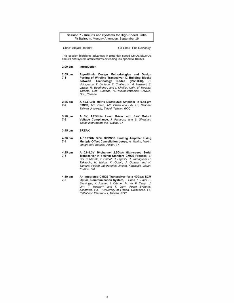
Session 7 - Circuits and Systems for High-Speed Links
Fir Ballroom, Monday Afternoon, September 19 Chair: Amjad Obeidat Co-Chair: Eric Naviasky This session highlights advances in ultra-high speed CMOS/BiCMOS circuits and system architectures extending link speed to 40Gb/s. 2:00 pm Introduction 2:05 pm 7-1
Algorithmic Design Methodologies and Design Porting of Wireline Transceiver IC Building Blocks between Technology Nodes (INVITED), S. Voinigescu, T. Dickson, T. Chalvatzis, A. Hazneci, E. Laskin, R. Beerkens*, and I. Khalid*, Univ. of Toronto, Toronto, Ont., Canada, *STMicroelectronics, Ottawa, Ont., Canada
2:55 pm 7-2
A 45.6-GHz Matrix Distributed Amplifier in 0.18-µm CMOS, T-Y. Chen, J-C. Chien and L-H. Lu, National Taiwan University, Taipei, Taiwan, ROC
3:20 pm 7-3
A 3V, 4.25Gb/s Laser Driver with 0.4V Output Voltage Compliance, J. Fattaruso and B. Sheahan, Texas Instruments Inc., Dallas, TX
3:45 pm BREAK 4:00 pm 7-4
A 10.7GHz SiGe BICMOS Limiting Amplifier Using Multiple Offset Cancellation Loops, A. Maxim, Maxim Integrated Products, Austin, TX
4:25 pm 7-5
A 0.8-1.3V 16-channel 2.5Gb/s High-speed Serial Transceiver in a 90nm Standard CMOS Process, Y. Doi, S. Masaki, T. Chiba*, H. Higashi, H. Yamaguchi, H. Takauchi, H. Ishida, K. Gotoh, J. Ogawa, and H. Tamura, Fujitsu Laboratories Limited, Kawasaki, Japan, *Fujitsu, Ltd.
4:50 pm 7-6
An Integrated CMOS Transceiver for a 40Gb/s SCM Optical Communication System, J. Chen, F. Saibi, E. Sackinger, K. Azadet, J. Othmer, M. Yu, F. Yang, J. Lin*, T. Huang**, and T. Liu**, Agere Systems, Allentown, PA, *University of Florida, Gainesville, FL, **Winbond Electronics, Taiwan, ROC
20
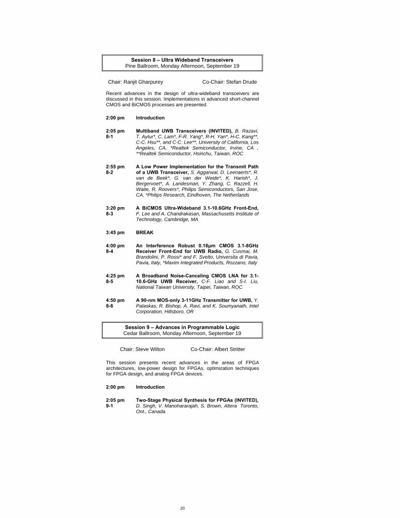
Session 8 – Ultra Wideband Transceivers
Pine Ballroom, Monday Afternoon, September 19 Chair: Ranjit Gharpurey Co-Chair: Stefan Drude
Recent advances in the design of ultra-wideband transceivers are discussed in this session. Implementations in advanced short-channel CMOS and BiCMOS processes are presented. 2:00 pm Introduction 2:05 pm 8-1
Multiband UWB Transceivers (INVITED), B. Razavi, T. Aytur*, C. Lam*, F-R. Yang*, R-H. Yan*, H-C. Kang**, C-C. Hsu**, and C-C. Lee**, University of California, Los Angeles, CA, *Realtek Semiconductor, Irvine, CA , **Realtek Semiconductor, Hsinchu, Taiwan, ROC
2:55 pm 8-2
A Low Power Implementation for the Transmit Path of a UWB Transceiver, S. Aggarwal, D. Leenaerts*, R. van de Beek*, G. van der Weide*, K. Harish*, J. Bergervoet*, A. Landesman, Y. Zhang, C. Razzell, H. Waite, R. Roovers*, Philips Semiconductors, San Jose, CA, *Philips Research, Eindhoven, The Netherlands
3:20 pm 8-3
A BiCMOS Ultra-Wideband 3.1-10.6GHz Front-End, F. Lee and A. Chandrakasan, Massachusetts Institute of Technology, Cambridge, MA
3:45 pm BREAK 4:00 pm 8-4
An Interference Robust 0.18µm CMOS 3.1-8GHz Receiver Front-End for UWB Radio, G. Cusmai, M. Brandolini, P. Rossi* and F. Svelto, Universita di Pavia, Pavia, Italy, *Maxim Integrated Products, Rozzano, Italy
4:25 pm 8-5
A Broadband Noise-Canceling CMOS LNA for 3.1-10.6-GHz UWB Receiver, C-F. Liao and S-I. Liu, National Taiwan University, Taipei, Taiwan, ROC
4:50 pm 8-6
A 90-nm MOS-only 3-11GHz Transmitter for UWB, Y. Palaskas, R. Bishop, A. Ravi, and K. Soumyanath, Intel Corporation, Hillsboro, OR
Session 9 – Advances in Programmable Logic
Cedar Ballroom, Monday Afternoon, September 19
Chair: Steve Wilton Co-Chair: Albert Stritter This session presents recent advances in the areas of FPGA architectures, low-power design for FPGAs, optimization techniques for FPGA design, and analog FPGA devices. 2:00 pm Introduction 2:05 pm 9-1
Two-Stage Physical Synthesis for FPGAs (INVITED), D. Singh, V. Manohararajah, S. Brown, Altera Toronto, Ont., Canada

21
2:55 pm 9-2
An Improved "Soft" eFPGA Design and Implementation Strategy, V. Aken'Ova, G. Lemieux, and R. Saleh, University of British Columbia, Vancouver, British Columbia, Canada
3:20 pm 9-3
Heterogeneous Routing Architecture for Low-Power FPGA Fabric, A. Rahman, S. Das, T. Tuan, and A. Rahut, Xilinx, Inc., San Jose, CA
3:45 pm BREAK 4:00 pm 9-4
Look-Up Table Leakage Reduction for FPGAs, N. Azizi and F. Najm, University of Toronto, Toronto, Ontario, Canada
4:25 pm 9-5
A Continuous-time Hierarchical Field Programmable Analogue Array, D. Varghese and J. Ross, University of Southampton, United Kingdom
Session 10 – Data Converters Oak Ballroom, Tuesday Morning, September 20
Chair: Kathleen Philips Co-Chair: David Nairn
Analog-to-Digital converters continue to push the performance envelope by exploiting newer processing technologies and by innovative improvements to known circuit techniques. 8:30 am Introduction 8:35 am 10-1
Scaling of Analog-to-Digital Converters into Ultra-Deep-Submicron CMOS (INVITED), Y. Chiu, B. Nikolic*, and P. Gray*, University of Illinois, Urbana, IL, *University of California at Berkeley, Berkeley, CA
9:25 am 10-2
A ∆Σ DAC with Reduced Activity Data Weighted Averaging and Anti-jitter Digital Filter, A. Bicakci and G. Singh, LSI Logic Corporation, Milpitas,CA
9:50 am BREAK 10:05 am 10-3
A 10.24GSPS Photonic Sampled Bandpass Delta-Sigma Modulator Direct-Sampling at 12GHz, L. Luh, W. Ng, J. Jensen, D. Le, D. Persechini, S. Thomas, C. Fields, and J. Lin, HRL Laboratories, LLC, Malibu, CA
10:30 am 10-4
A 14-bit 125 MS/s IF/RF Sampling Pipelined A/D Converter, A. Ali, C. Dillon, R. Sneed, A. Morgan, J. Kornblum, L. Wu, and S. Bardsley, Analog Devices, Inc., Greensboro, NC
10:55 am 10-5
A 1.0V 40mW 10b 100MS/s Pipeline ADC in 90nm CMOS, H. Ishii, K. Tanabe, and T. Iida, Toshiba Corporation, Kawasaki, Japan
22
11:20 am 10-6
A 50MS/s 12-bit CMOS Pipeline A/D Converter with Nonlinear Background Calibration, J. Yuan, N. Farhat, and J. Van der Spiegel, University of Pennsylvania, Philadelphia, PA
11:45 am 10-7
Dual Scalable 500MS/s, 5b Time-Interleaved SAR ADCs for UWB Applications, B. Ginsburg and A. Chandrakasan, Massachusetts Institute of Technology, Cambridge, MA
Session 11 – High-Speed Wave-Shaping Techniques Fir Ballroom, Tuesday Morning, September 20
Chair: Shahriar Mirabbasi Co-Chair: Cormac O’Connell
In this session, advanced techniques to improve signal integrity and to achieve high-speed communication over band-limited media are presented. 8:30 am Introduction 8:35 am 11-1
Crosstalk-Induced Jitter Equalization, J. Buckwalter and A. Hajimiri, California Institute of Technology, Pasadena, CA
9:00 am 11-2
A Continuous-Time Adaptive FIR Equalizer with INV-AIL Delay Line for 2.5Gb/s Data Communication, X. Lin, H. Lee*, and J. Liu*, Texas Instruments Inc., Dallas, TX, *University of Texas at Dallas, Richardson, TX
9:25 am 11-3
A 40Gb/s Transversal Filter in 0.18µm CMOS Using Distributed Amplifiers, J. Sewter and A. Chan Carusone, University of Toronto, Toronto, Ont., Canada
9:50 am BREAK
Session 12 - Memory Circuits and Technology Pine Ballroom, Tuesday Morning, September 20
Chair: Takashi Akioka Co-Chair: Jean-Christophe Vial
This session begins with an overview of emerging memories. Also presented are high-density ferroelectric, phase-change and capacitorless gain cell memories. This is followed by two SRAM stability analyses, and two interesting CAM architectures. 8:30 am Introduction 8:35 am 12-1
Emerging Memory Technologies (INVITED), K. Kim, G. Jeong, H. Jeong, and S. Lee, Samsung Electronics Co., Ltd., Gyeonggi-Do, Korea
23
9:00 am 12-2
An 8Mb 1T1C Ferroelectric Memory With Zero Cancellation and Micro-Granularity Redundancy, J. Eliason, S. Madan*, H. McAdams*, G. Fox, T. Moise*, C. Lin, K. Schwartz, J. Gallia*, E. Jabillo, B. Kraus, and S. Summerfelt*, Ramtron International Corporation, Colorado Springs, CO, *Texas Instruments Inc., Dallas, TX
9:25 am 12-3
Phase Change RAM Operated with 1.5-V CMOS as Low Cost Embedded Memory, K. Osada, T. Kawahara, R. Takemura, N. Kitai*, N. Takaura, N. Matsuzaki, K. Kurotsuchi, H. Moriya+, and M. Moniwa^, Hitachi, Ltd., Tokyo, Japan, +Hitachi, Ltd., Ibaraki, Japan, *Hitachi ULSI Systems Co., Tokyo, Japan, ^Renesas Technology Corporation, Hyogo, Japan
9:50 am BREAK 10:05 am 12-4
A Capacitorless Twin-Transistor Random Access Memory (TTRAM) on SOI, F. Morishita, H. Noda, T. Gyohten, M. Okamoto*, T. Ipposhi, S. Maegawa, K. Dosaka, and K. Arimoto, Renesas Technology Corporation, Hyogo, Japan, *Daioh Electric Corporation, Hyogo, Japan
10:30 am 12-5
Fast and Accurate Estimation of Nano-Scaled SRAM Read Failure Probability Using Critical Point Sampling, I.J. Chang, K. Kang, S. Mukhopadhyay, C.H. Kim*, and K. Roy, Purdue University, West Lafayette, IN, *University of Minnesota, Minneapolis, MN
10:55 am 12-6
Programmable Techniques for Cell Stability Test and Debug in Embedded SRAMs, A. Pavlov, M. Sachdev, J. Pineda de Gyvez*, and M. Azimane* , University of Waterloo, Ontario, Canada, *Philips Research Labs, Eindhoven, The Netherlands
11:20 am 12-7
Low-Noise Embedded CAM with Reduced Slew-rate Match-lines and Asynchronous Search-lines, I. Arsovski and R. Nadkarni, IBM, Essex Junction, VT
11:45 am 12-8
A Soft-Error-Immune Maintenance-Free TCAM Architecture with Associated Embedded DRAM, H. Noda, K. Dosaka, F. Morishita, and K. Arimoto, Renesas Technology Corporation, Hyogo, Japan
Session 13 – Substrate and Phase-Noise Characterization
Cedar Ballroom, Tuesday Morning, September 20 Chair: Steffen Rochel Co-Chair: Hidetoshi Onodera This session presents new techniques to determine the characteristics of oscillators followed by advanced substrate-noise modeling methods and design applications. 8:30 am Introduction 8:35 am 13-1
Phase Noise in Inverter-Based & Differential CMOS Ring Oscillators, A. Abidi and S. Samadian, University of California, Los Angeles, CA

24
9:00 am 13-2
Analytical Equations For Predicting Injection Locking in LC and Ring Oscillators, X. Lai and J. Roychowdhury, University of Minnesota, Minneapolis, MN
9:25 am 13-3
A Multiple-Probe Approach for Robust Frequency Domain Ring Oscillator Simulation, X. Duan and K. Mayaram, Oregon State University, Corvallis, OR
9:50 am BREAK 10:05 am 13-4
Synthesized Compact Model and Experimental Results for Substrate Noise Coupling in Lightly Doped Processes, H. Lan, T. Chen, C. Chui, P. Nikaeen, J.W. Kim, and R. Dutton, Stanford University, Stanford, CA
10:30 am 13-5
Substrate Noise Analysis and Experimental Verification for the Efficient Noise Prediction of a Digital PLL, N. Checka, A. Chandrakasan, and R. Reif, Massachusetts Institute of Technology, Cambridge, MA
10:55 am 13-6
Substrate Noise Immune Design of an LC-tank VCO Using Sensitivity Functions, C. Soens, G. Van der Plas, P. Wambacq, and S. Donnay, IMEC, Leuven, Belgium
Session 14 - ESD Implementation Strategies Fir Ballroom, Tuesday Morning, September 20
Chair: Mike Zachariah Co-Chair: Rob Aitken
This session consists of two tutorial presentations on ESD protection circuits and strategies, followed by a specific RF example consisting of an LNA and VCO. 10:00 am Introduction 10:05 am 14-1
Advanced SCR ESD Protection Circuits for CMOS/SOI Nanotechnologies (INVITED), M. Mergens*, O. Marichal, S. Thijs, B. Van Camp, and C. Russ*, Sarnoff Europe, Gistel, Belgium, *Infineon Technologies AG, Munich, Germany
10:55 am 14-2
RF ESD Protection Strategies - The Design and Performance Trade-off Challenges (INVITED), P. Jansen, S. Thijs, D. Linten, M. Natarajan, V. Vassilev, M. Liu, A. Concannon*, D. Trémouilles, T. Nakaie+, M. Sawada+, M. ter Beek*, V. Vashchenko*, T. Hasebe+, S. Decoutere, and G. Groeseneken, IMEC, Leuven, Belgium, *National Semiconductor Corp., Santa Clara, CA, +Hanwa Electronic Industries, Wakayama, Japan
11:45 am 14-3
Low-Power Low-Noise Highly ESD Robust LNA, and VCO Design Using Above-IC Inductors, D. Linten, X. Sun, S. Thijs, M. Natarajan, A. Mercha, G. Carchon, P. Wambacq, T. Nakaie, S. Decoutere, IMEC, Leuven, Belgium
25
CICC Luncheon Sierra Ballroom, Tuesday, September 20
12:00 – 1:30 pm
Automotive Electronics: Steady Growth for Years to Come Dr. Alberto Sangiovanni-Vincentelli
The Edgar L. and Harold H. Buttner Chair of Electrical Engineering and Computer Science, Univ. of California, Berkeley
The world of electronics is witnessing a revolution in the way products are conceived, designed and implemented. The ever growing importance of the web, the advent of microprocessors of great computational power, the explosion of wireless communication, and the development of new generations of integrated sensors and actuators are changing the world in which we live and work.
The car as a self-contained microcosm is experiencing a similar revolution. We need to rethink what a “car’ really is and the role of electronics in it. Electronics is now essential to control the movements of a car, of the chemical and electrical processes taking place in it, to entertain the passengers, to establish connectivity with the rest of the world, and to ensure safety. What will an automobile manufacturer’s core competence become in the next few years? Will electronics be the essential element in car manufacturing and design? The challenges and opportunities are related to: • how to integrate the mechanical and the electronics worlds
(mechatronics) • how to integrate the different motion control and power-train
control functions to exploit important synergies • how to combine entertainment, communication and navigation
subsystems • how to couple the world of electronics where the lifetime of a
product is around two years and shrinking, with the automotive world, where the product lifetime is 10 years and possibly growing
• how to develop new services based on electronics technology • how are the markets changing, such as, after-market sales for
automotive electronics, if any? We will pose these questions while reviewing some of the most important technology and product developments of the past few years. We will also present new trends on how the design of electronics of the car should be carried out. We will finally analyze the dynamics of the automotive electronics industry that is bound to produce a major shakeup in the structure of the design chain.

26
Session 15 – Custom Circuits
Oak Ballroom, Tuesday Afternoon, September 20
Chair: Jamil Kawa Co-Chair: Jackie Snyder This session focuses on custom circuits covering a wide spectrum of applications. It includes differential ring oscillators, a high throughput driver, CMOS-MEM pressure sensors, an analog broadband transceiver, a write divider with overshoot control, a monolithic clock synthesizer, and a conditional clocking low-power flip-flop. 2:00 pm Introduction 2:05 pm 15-1
Differential Ring Oscillators with Multipath Delay Stages, S. Mohan, W. S. Chan*, D. Colleran, S. Greenwood**, J. Gamble+ and I. Kouznetsov^ Sabio Labs, Palo Alto, CA, *Marvell Semiconductor, Sunnyvale, CA, **ATI Technologies, Sunnyvale, CA, +Synopsys, Hillsboro, OR, ^Cypress Semiconductor, San Jose, CA
2:30 pm 15-2
A High Throughput Divider Implementation, X. Guo and C. Sechen, University of Washington, Seattle, WA
2:55 pm 15-3
Piezoresistive CMOS-MEMS Pressure Sensor with Ring Oscillator Readout Including Delta-Sigma Analog-to-Digital Converter On-chip, K. Øysted and D. Wisland, University of Oslo, Oslo, Norway
3:20 pm 15-4
A Highly-Integrated CMOS Analog Baseband Transceiver with 180MSPS 13b Pipelined CMOS ADC and Dual 12b DACs, K. Gulati, M. Peng, A. Pulincherry, C. Muñoz, M. Lugin, A. Bugeja, J. Li, and A. Chandrakasan*, Engim, Inc., Acton, MA, *Massachusetts Institute of Technology, Cambridge, MA
3:45 pm BREAK 4:00 pm 15-5
A 1.2Gb/s Write Driver with Pre-emphasis Overshoot Control Optimized for High Density HDD Applications, Y. Hayashi, M. Sonehara, S. Ueno, Y. Ito, A. Koyama, and H. Yamashita, Hitachi, Ltd., Tokyo, Japan
4:25 pm 15-6
A 9.2mW 528/66/50MHz Monolithic Clock Synthesizer for Mobile µP Platforms, M. McCorquodale, S. Pernia, J. O'Day, G. Carichner, and S. Kubba, Mobius Microsystems Inc., Detroit, MI
4:50 pm 15-7
A Conditional Clocking Flip-Flop for Low Power H.264/MPEG-4 Audio/Visual Codec LSI, M. Hamada, H. Hara, T. Fujita, C.K. Teh, T. Shimazawa, N. Kawabe, T. Kitahara, Y. Kikuchi, T. Nishikawa, M. Takahashi, and Y. Oowaki, Toshiba Corporation, Kawasaki, Japan
27
Session 16 – Clocking Circuits for Wireline Communications
Fir Ballroom, Tuesday Afternoon, September 20
Chair: Jafar Savoj Co-Chair: Ramesh Harjani
This session presents novel techniques to improve signal purity in wireline systems. Topics include oscillator design, PLL and DLL architectures, and CDR circuits. 2:00 pm Introduction 2:05 pm 16-1
Low Voltage Wide Range DLL-based Quad-phase Core Clock Generator for High Speed Network SRAM Application, N-S. Kim, U-R. Cho, and H-G. Byun, Samsung Electronics, Kyeonggi-Do, Korea
2:30 pm 16-2
A Digital Clock and Data Recovery Architecture for Multi-Gigabit/s Binary Links (INVITED), J. Sonntag and J. Stonick, Synopsys, Inc., Hillsboro, OR
3:20 pm 16-3
9.953-12.5GHz 0.13µm CMOS LC VCO Using a High Resolution Calibration and a Constant Gain Varactor, A. Maxim and C. Turinici, Integrated Products, Austin, TX
3:45 pm BREAK 4:00 pm 16-4
An Improved Wideband PLL with Adaptive Frequency Response that Tracks the Reference, M. Hufford, E. Naviasky, S. Williams, and M. Williams, Cadence Design Services, Columbia, MD
4:25 pm 16-5
A Versatile Low-Jitter PLL in 90-nm CMOS for SerDes Transmitter Clocking, A. Loke, R. Barnes, T-T. Wee, M. Oshima*, C. Moore, R. Kennedy, J. Barnes, R. Zimmer, K. Arave, H. Pang, T. Cynkar, A. Volz, J. Pfiester, R. Martin, R. Miller, D. Hood, G. Motley, E. Rojas, T. Walley, M. Gilsdorf, Agilent Technologies, Fort Collins, CO, *Agilent Technologies, Santa Clara, CA
4:50 pm 16-6
A Full-Rate Injection-Locked 10.3Gb/s Clock and Data Recovery Circuit in a 45GHz-fT SiGe Process, J-H. C. Zhan, J. Duster, and K. Kornegay, Cornell University, Ithaca, NY
Session 17 – Silicon Millimeter Wave ICs, VCOs, and Dividers
Pine Ballroom, Tuesday Afternoon, September 20 Chair: Kevin Kornegay Co-Chair: Nobuyuki Itoh This session presents advances in silicon millimeter wave IC, VCO, and divider design. Applications at 60GHz and 77GHz are described along with novel circuit-area and phase-noise reduction techniques. Lastly, innovative circuits for quadrature LO generation are presented. 2:00 pm Introduction
28
2:05 pm 17-1
Progress Toward a Low-Cost Millimeter-Wave Silicon Radio (INVITED), S. Reynolds, B. Floyd, U. Pfeiffer, T. Beukema, T. Zwick, J. Grzyb, D. Liu, and B. Gaucher, IBM T.J. Watson Research Center, Yorktown Heights, NY
2:55 pm 17-2
A Wideband 77GHz, 17.5dBm Power Amplifier in Silicon, A. Komijani and A. Hajimiri, California Institute of Technology, Pasadena, CA
3:20 pm 17-3
Balanced CMOS LC-tank Analog Frequency Dividers for Quadrature LO Generation, A. Mazzanti, L. Larcher*, and F. Svelto**, Universita di Modena e Reggio Emilia, Modena, Italy *Universita di Modena e Reggio Emilia, Reggio Emilia, Italy, **Universita di Pavia, Pavia, Italy
3:45 pm BREAK 4:00 pm 17-4
A Tail Current-Shaping Technique to Reduce Phase Noise in LC VCOs, B. Soltanian and P. Kinget, Columbia University, New York, NY
4:25 pm 17-5
A Phase Noise Minimization of CMOS VCOs Over Wide Tuning Range and Large PVT Variations, D. Miyashita, H. Ishikuro, S. Kousai, H. Kobayashi, H. Majima, K. Agawa, and M. Hamada, Toshiba Corporation, Kawasaki, Japan
4:50 pm 17-6
Voltage-Controlled Oscillator in the Coil, F. Zhang, C-F. Chu, and P. Kinget, Columbia University, New York, NY
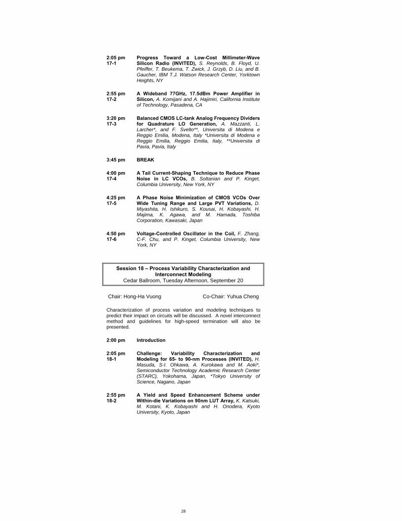
Session 18 – Process Variability Characterization and Interconnect Modeling
Cedar Ballroom, Tuesday Afternoon, September 20 Chair: Hong-Ha Vuong Co-Chair: Yuhua Cheng Characterization of process variation and modeling techniques to predict their impact on circuits will be discussed. A novel interconnect method and guidelines for high-speed termination will also be presented. 2:00 pm Introduction 2:05 pm 18-1
Challenge: Variability Characterization and Modeling for 65- to 90-nm Processes (INVITED), H. Masuda, S-I. Ohkawa, A. Kurokawa and M. Aoki*, Semiconductor Technology Academic Research Center (STARC), Yokohama, Japan, *Tokyo University of Science, Nagano, Japan
2:55 pm 18-2
A Yield and Speed Enhancement Scheme under Within-die Variations on 90nm LUT Array, K. Katsuki, M. Kotani, K. Kobayashi and H. Onodera, Kyoto University, Kyoto, Japan

29
3:20 pm 18-3
Characterization of Deep-Submicron Varactor Mismatches in a Digitally Controlled Oscillator, K. Waheed and R. Staszewski, Texas Instruments Inc., Dallas ,TX
3:45 pm BREAK 4:00 pm 18-4
Modeling Leakage in ASIC Libraries, S. Lichtensteiger, L. Wissel, J. Engel, and P. Sulva, IBM Microelectronics, Essex Junction, VT
4:25 pm 18-5
Design Guideline for Resistive Termination of On-Chip High-Speed Interconnects, A. Tsuchiya, M. Hashimoto*, and H. Onodera, Kyoto University, Kyoto, Japan, *Osaka University, Suita, Osaka, Japan
4:50 pm 18-6
A Novel Global Interconnect Method Using Nonlinear Transmission Lines, J. Kim, W. Ni, and E.C. Kan, Cornell University, Ithaca, NY
Session 19 – Evening Panel Discussion Oak Ballroom, Tuesday Evening, September 20
Will Continued Process-Node Shrinks Kill
High-Performance Analog Design? Organizer: Jafar Savoj, Marvell Semiconductor Moderator: David Rich, Consultant Panelists: Brett Forejt Texas Instruments Peter Kinget Columbia University Un-Ku Moon Oregon State University Modest Oprysko IBM
Behzad Razavi UCLA Hisashi (Sam) Shichijo Texas Instruments Albert Wang Illinois Institute of Technology
“Digital designers to take over the world when analog designers produce 10 Gbps 18-bit data converters that attach to antennas."
This may be a dream, but many next-generation analog systems need high resolution (>12 bits) circuits that run at higher sampling rates. PLL designers can push the speed envelope, but what about other analog blocks? Has scaling finally driven analog design off the submicron roadmap as supply voltages dip below 1V and devices have more leakage paths than the average basement? Come hear gurus debate the realities of the state-of-the-art transistor from now until the end of the decade. Learn what's ahead with transistors that will be able to do little more than divide by two at 500 GHz clock rates.
30
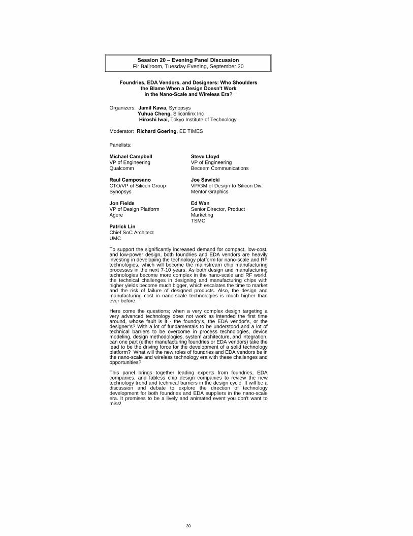
Session 20 – Evening Panel Discussion
Fir Ballroom, Tuesday Evening, September 20
Foundries, EDA Vendors, and Designers: Who Shoulders the Blame When a Design Doesn't Work
in the Nano-Scale and Wireless Era? Organizers: Jamil Kawa, Synopsys Yuhua Cheng, Siliconlinx Inc Hiroshi Iwai, Tokyo Institute of Technology Moderator: Richard Goering, EE TIMES Panelists: Michael Campbell VP of Engineering Qualcomm Raul Camposano CTO/VP of Silicon Group Synopsys Jon Fields VP of Design Platform Agere Patrick Lin Chief SoC Architect UMC
Steve Lloyd VP of Engineering Beceem Communications Joe Sawicki VP/GM of Design-to-Silicon Div. Mentor Graphics Ed Wan Senior Director, Product Marketing TSMC
To support the significantly increased demand for compact, low-cost, and low-power design, both foundries and EDA vendors are heavily investing in developing the technology platform for nano-scale and RF technologies, which will become the mainstream chip manufacturing processes in the next 7-10 years. As both design and manufacturing technologies become more complex in the nano-scale and RF world, the technical challenges in designing and manufacturing chips with higher yields become much bigger, which escalates the time to market and the risk of failure of designed products. Also, the design and manufacturing cost in nano-scale technologies is much higher than ever before. Here come the questions; when a very complex design targeting a very advanced technology does not work as intended the first time around, whose fault is it - the foundry’s, the EDA vendor’s, or the designer’s? With a lot of fundamentals to be understood and a lot of technical barriers to be overcome in process technologies, device modeling, design methodologies, system architecture, and integration, can one part (either manufacturing foundries or EDA vendors) take the lead to be the driving force for the development of a solid technology platform? What will the new roles of foundries and EDA vendors be in the nano-scale and wireless technology era with these challenges and opportunities? This panel brings together leading experts from foundries, EDA companies, and fabless chip design companies to review the new technology trend and technical barriers in the design cycle. It will be a discussion and debate to explore the direction of technology development for both foundries and EDA suppliers in the nano-scale era. It promises to be a lively and animated event you don't want to miss!
31
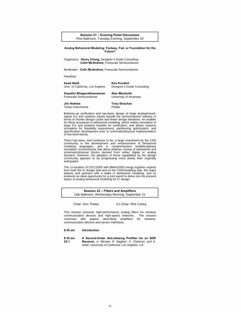
Session 21 – Evening Panel Discussion Pine Ballroom, Tuesday Evening, September 20
Analog Behavioral Modeling: Fantasy, Fad, or Foundation for the
Future? Organizers: Henry Chang, Designer’s Guide Consulting Colin McAndrew, Freescale Semiconductor Moderator: Colin McAndrew, Freescale Semiconductor Panelists: Asad Abidi Univ. of California, Los Angeles Gayathri Bhagavatheeswaran Freescale Semiconductor Jim Holmes Texas Instruments
Ken Kundert Designer’s Guide Consulting Alan Mantooth University of Arkansas Tony Strachan Philips
Bottoms-up verification and top-down design of large analog/mixed-signal ICs and systems clearly benefit the semiconductor industry in terms of shorter design cycles and fewer design iterations. An enabler for these processes is behavioral modeling, which makes simulation of large ICs and systems feasible for verification, and allows systems simulation for feasibility assessment, partitioning optimization, and specification development prior to schematic/physical implementation of low-level blocks. There has been, and continues to be, a large investment by the CAD community in the development and enhancement of behavioral modeling languages, and in comprehensive multidisciplinary simulation environments that allow arbitrary mixing of behavioral and schematic/physical blocks derived from either digital or analog domains. However, the adoption of these capabilities by the design community appears to be progressing more slowly than originally anticipated. The co-location of CICC2005 with BMAS2005 brings together experts from both the IC design side and on the CAD/modeling side, the major players and partners with a stake in behavioral modeling, and so presents an ideal opportunity for a joint panel to delve into the present status of analog behavioral modeling for IC design.
Session 22 – Filters and Amplifiers Oak Ballroom, Wednesday Morning, September 21
Chair: Don Thelen Co-Chair: Rick Carley
This session presents high-performance analog filters for wireless communication devices and high-speed networks. The session continues with papers describing amplifiers for wireless- communication devices and sensor interfaces. 8:30 am Introduction 8:35 am 22-1
A Second-Order Anti-aliasing Prefilter for an SDR Receiver, A. Mirzaei, R. Bagheri, S. Chehrazi, and A. Abidi, University of California, Los Angeles, CA
32
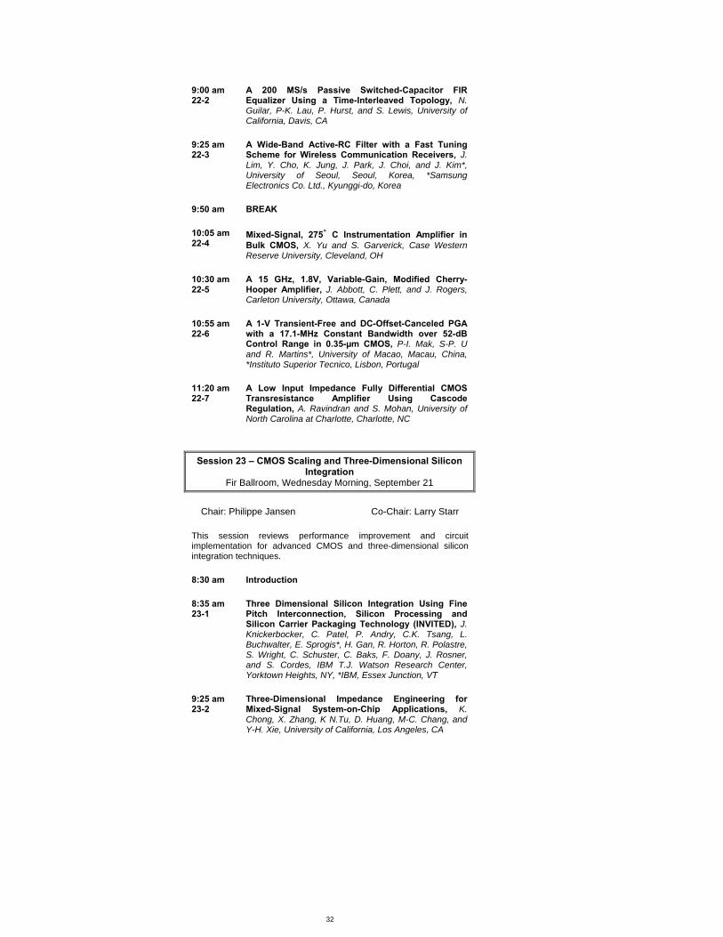
9:00 am 22-2
A 200 MS/s Passive Switched-Capacitor FIR Equalizer Using a Time-Interleaved Topology, N. Guilar, P-K. Lau, P. Hurst, and S. Lewis, University of California, Davis, CA
9:25 am 22-3
A Wide-Band Active-RC Filter with a Fast Tuning Scheme for Wireless Communication Receivers, J. Lim, Y. Cho, K. Jung, J. Park, J. Choi, and J. Kim*, University of Seoul, Seoul, Korea, *Samsung Electronics Co. Ltd., Kyunggi-do, Korea
9:50 am BREAK 10:05 am 22-4
Mixed-Signal, 275˚ C Instrumentation Amplifier in Bulk CMOS, X. Yu and S. Garverick, Case Western Reserve University, Cleveland, OH
10:30 am 22-5
A 15 GHz, 1.8V, Variable-Gain, Modified Cherry-Hooper Amplifier, J. Abbott, C. Plett, and J. Rogers, Carleton University, Ottawa, Canada
10:55 am 22-6
A 1-V Transient-Free and DC-Offset-Canceled PGA with a 17.1-MHz Constant Bandwidth over 52-dB Control Range in 0.35-µm CMOS, P-I. Mak, S-P. U and R. Martins*, University of Macao, Macau, China, *Instituto Superior Tecnico, Lisbon, Portugal
11:20 am 22-7
A Low Input Impedance Fully Differential CMOS Transresistance Amplifier Using Cascode Regulation, A. Ravindran and S. Mohan, University of North Carolina at Charlotte, Charlotte, NC
Session 23 – CMOS Scaling and Three-Dimensional Silicon
Integration Fir Ballroom, Wednesday Morning, September 21
Chair: Philippe Jansen Co-Chair: Larry Starr
This session reviews performance improvement and circuit implementation for advanced CMOS and three-dimensional silicon integration techniques. 8:30 am Introduction 8:35 am 23-1
Three Dimensional Silicon Integration Using Fine Pitch Interconnection, Silicon Processing and Silicon Carrier Packaging Technology (INVITED), J. Knickerbocker, C. Patel, P. Andry, C.K. Tsang, L. Buchwalter, E. Sprogis*, H. Gan, R. Horton, R. Polastre, S. Wright, C. Schuster, C. Baks, F. Doany, J. Rosner, and S. Cordes, IBM T.J. Watson Research Center, Yorktown Heights, NY, *IBM, Essex Junction, VT
9:25 am 23-2
Three-Dimensional Impedance Engineering for Mixed-Signal System-on-Chip Applications, K. Chong, X. Zhang, K N.Tu, D. Huang, M-C. Chang, and Y-H. Xie, University of California, Los Angeles, CA

33
9:50 am BREAK 10:05 am 23-3
Strain for CMOS Performance Improvement (INVITED), V. Chan, K. Rim, M. Ieong*, S. Yang, R. Malik, Y. Teh**, M. Yang*, Q. Ouyang*, IBM Systems & Technology Group, *IBM T.J. Watson Research Center, **Chartered Semiconductor Mfg., Ltd.
10:55 am 23-4
Device Trends and Implications on Circuit Design in Advanced CMOS Technologies (INVITED), C. Diaz, H.K. Fung, Y.K. Leung, C.C. Wu, C.P. Chao, G. Chern, W. Lin, C. Lee, F.S. Lai, M.C. Chang and Y.C. Sun, TSMC, Taiwan, ROC
Session 24 – Signal and Data Processors Pine Ballroom, Wednesday Morning, September 21
Chair: Dawn Fitzgerald Co-Chair: Bryan Ackland This session presents signal-processing algorithms and architectures that provide high-performance, low-power solutions in storage, multimedia and communications applications. 8:30 am Introduction 8:35 am 24-1
Digital Signal Processing in Read Channels (INVITED), E. Haratsch and Z. Keirn, Agere Systems, Allentown, PA
9:25 am 24-2
An ASIC Implementation of JPEG2000 Codec, L. Liu, H-Y. Meng, L. Zhang, and Z. Wang, Tsinghua University, Beijing, China
9:50 am BREAK 10:05 am 24-3
A Continuous-Time Programmable Digital FIR Filter, Y. W. Li, K. Shepard, and Y. Tsividis, Columbia University, New York, NY
10:30 am 24-4
An (8158,7136) Low-Density Parity-Check Encoder, L. Miles, J. Gambles, G. Maki, W. Ryan* and S. Whitaker, University of Idaho, Post Falls, ID, *University of Arizona, Tucson, AZ
10:55 am 24-5
Loosely Coupled Memory-Based Decoding Architecture for Low Density Parity Check Codes, S-H. Kang and I-C. Park, Korea Advanced Institute of Science and Technology, Daejeon, Korea

34
Session 25 – Behavioral Modeling and Simulation Cedar Ballroom, Wednesday Morning, September 21
Chair: Jeanne Trinko Mechler Co-Chair: Larry Nagel
This session features behavioral modeling to enable rapid simulation and verification of complex non-linear circuits, as well as complex high-speed systems, such as serial links. 8:30 am Introduction 8:35 am 25-1
Modeling, Simulation, and Design of a Multi-Mode 2-10 Gb/sec Fully Adaptive Serial Link System (INVITED), C. Werner, C. Høyer*, A. Ho, M. Jeeradit, F. Chen, B. Garlepp, W. Stonecypher, S. Li, A. Bansal, A. Agarwal, E. Alon**, V. Stojanovic*** and J. Zerbe, Rambus, Inc., Los Altos, CA, *Enigma Semiconductor, Copenhagen, Denmark, **Stanford University, Stanford, CA, ***Massachusetts Institute of Technology, Cambridge, MA
9:25 am 25-2
A Behavioral Level Approach for Nonlinear Dynamic Modeling of Voltage-Controlled Oscillators, R. Batra, P. Li*, L. Pileggi, and W-J. Chiang**, Carnegie Mellon University, Pittsburgh, PA, *Texas A&M University, College Station, TX, **Industrial Technology Research Institute, Hsinchu, Taiwan, ROC
9:50 am BREAK 10:05 am 25-3
Model Topology Formulation for Nonlinear Dynamic Behavioral Modeling, Y. Feng, W. Zheng, X. Huang, and H. Mantooth, University of Arkansas, Fayetteville, AR
10:30 am 25-4
A Signal Integrity-based Link Performance Simulation Platform, Y. Tao, W. Bereza, R. Patel*, S. Shumarayev* and T. Kwasniewski, Altera Corporation, Ottawa, Ontario, Canada, *Altera Corporation, San Jose, CA
10:55 am 25-5
Understanding Injection Locking in Negative-Resistance LC Oscillators Intuitively Using Nonlinear Feedback Analysis, Y. Wan, X. Lai and J. Roychowdhury, University of Minnesota, Minneapolis, MN
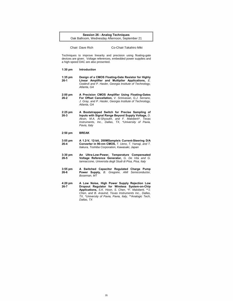
35
Session 26 - Analog Techniques
Oak Ballroom, Wednesday Afternoon, September 21
Chair: Dave Rich Co-Chair:Takahiro Miki Techniques to improve linearity and precision using floating-gate devices are given. Voltage references, embedded power supplies and a high-speed DAC are also presented. 1:30 pm Introduction 1:35 pm 26-1
Design of a CMOS Floating-Gate Resistor for Highly Linear Amplifier and Multiplier Applications, E. Ozalevli and P. Hasler, Georgia Institute of Technology, Atlanta, GA
2:00 pm 26-2
A Precision CMOS Amplifier Using Floating-Gates For Offset Cancellation, V. Srinivasan, G.J. Serrano, J. Gray, and P. Hasler, Georgia Institute of Technology, Atlanta, GA
2:25 pm 26-3
A Bootstrapped Switch for Precise Sampling of Inputs with Signal Range Beyond Supply Voltage, D. Aksin, M.A. Al-Shyoukh, and F. Maloberti*, Texas Instruments, Inc., Dallas, TX, *University of Pavia, Pavia, Italy
2:50 pm BREAK 3:05 pm 26-4
A 1.2-V, 12-bit, 200MSample/s Current-Steering D/A Converter in 90-nm CMOS, T. Ueno, T. Yamaji, and T. Itakura, Toshiba Corporation, Kawasaki, Japan
3:30 pm 26-5
An Ultra-Low-Power, Temperature Compensated Voltage Reference Generator, G. De Vita and G. Iannaccone, Universita degli Studi di Pisa, Pisa, Italy
3:55 pm 26-6
A Switched Capacitor Regulated Charge Pump Power Supply, B. Gregoire, AMI Semiconductor, Boseman, MT
4:20 pm 26-7
A Low Noise, High Power Supply Rejection Low Dropout Regulator for Wireless System-on-Chip Applications, S.K. Hoon, S. Chen, *F. Maloberti, **J. Chen, and B. Aravind, Texas Instruments Inc., Dallas, TX, *University of Pavia, Pavia, Italy, **Analogic Tech, Dallas, TX

36
Session 27 – Nanometer Design Intricacies
Fir Ballroom, Wednesday Afternoon, September 21
Chair: Rakesh Patel Co-Chair: Paul Billig
Nanometer processes are changing the norm in design approaches as technology scales. SoC/SIP, system-level architecture partitioning and power, and clock and IP reuse issues are becoming more prevalent to meet market timing and pricing goals. 1:30 pm Introduction 1:35 pm 27-1
Cellular Handset Integration - SIP vs SOC and Best Design Practices for SIP (INVITED), K. Lyne, Texas Instruments Inc., Dallas, TX
2:25 pm 27-2
A 90nm Power Optimization Methodology and Its Application to the ARM 1136JF-S Microprocessor, A. Khan, P. Watson*, G. Kuo, D. Le, T. Nguyen, S. Yang, P. Bennet, P. Huang, J. Gill, D. Wang, I. Ahmed, P. Tran, H. Mak, O. Kim, F. Martin, Y. Fan, D. Ge, J. Kung, and V. Shek, Cadence Design Systems, Inc., San Jose, CA, *ARM, Ltd., Cambridge, United Kingdom
2:50 pm BREAK 3:05 pm 27-3
Gated Decap: Gate Leakage Control of On-chip Decoupling Capacitors in Scaled Technologies, Y. Chen, H. Li*, K. Roy, C-K. Koh, Purdue University, West Lafayette, IN, *Qualcomm Inc., San Diego, CA
3:30 pm 27-4
A Comparison of Electrical and Optical Clock Networks in Nanometer Technologies, B. Ackland and B. Razavi*, L. West, Applied Materials, Santa Clara, CA, *University of California, Los Angeles, CA
3:55 pm 27-5
Multi-protocol Embedded PCS IP in a FPGA - SOC, R. Venkata, V. Chan, B. Ton, C. Lee, H. Ngo, M. Kabani, T. Nguyen, A. Zaliznyak, N. Xue, S. Shen, M. Zheng, M. Lai, S. Park, L. Chan, D. Vijayaraghavan, J. Lam, and R. Patel, Altera Corporation, San Jose, CA
4:20 pm 27-6
Elastic Shared Resource Scheduling SOC Interconnect Architecture for Real-time System, M. Saen, H. Ueda*, M. Hase*, E. Yamamoto*, Y. Mori*, H. Hatae*, Y. Kondo, S. Miura, I. Nonomura, N. Irie, and H. Watanabe*, Hitachi, Ltd., Tokyo, Japan; *Renesas Technology Corp., Tokyo, Japan
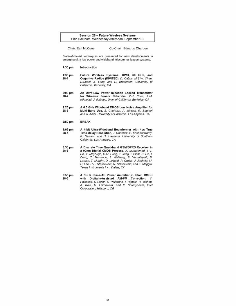
37
Session 28 – Future Wireless Systems
Pine Ballroom, Wednesday Afternoon, September 21
Chair: Earl McCune Co-Chair: Edoardo Charbon State-of-the-art techniques are presented for new developments in emerging ultra low power and wideband telecommunication systems. 1:30 pm Introduction 1:35 pm 28-1
Future Wireless Systems: UWB, 60 GHz, and Cognitive Radios (INVITED), D. Cabric, M.S.W. Chen, D.Sobel, J. Yang, and R. Brodersen, University of California, Berkeley, CA
2:00 pm 28-2
An Ultra-Low Power Injection Locked Transmitter for Wireless Sensor Networks, Y.H. Chee, A.M. Niknejad, J. Rabaey, Univ. of California, Berkeley, CA
2:25 pm 28-3
A 6.5 GHz Wideband CMOS Low Noise Amplifier for Multi-Band Use, S. Chehrazi, A. Mirzaei, R. Bagheri and A. Abidi, University of California, Los Angeles, CA
2:50 pm BREAK 3:05 pm 28-4
A 4-bit Ultra-Wideband Beamformer with 4ps True Time Delay Resolution, J. Roderick, H. Krishnaswamy, K. Newton, and H. Hashemi, University of Southern California, Los Angeles, CA
3:30 pm 28-5
A Discrete Time Quad-band GSM/GPRS Receiver in a 90nm Digital CMOS Process, K. Muhammad, Y-C. Ho, T. Mayhugh, C-M. Hung, T. Jung, I. Elahi, C. Lin, I. Deng, C. Fernando, J. Wallberg, S. Vemulapalli, S. Larson, T. Murphy, D. Leipold, P. Cruise, J. Jaehnig, M-C. Lee, R.B. Staszewski, R. Staszewski, and K. Maggio, Texas Instruments Inc., Dallas, TX
3:55 pm 28-6
A 5GHz Class-AB Power Amplifier in 90nm CMOS with Digitally-Assisted AM-PM Correction, Y. Palaskas, S.Taylor, S. Pellerano, I. Rippke, R. Bishop, A. Ravi, H. Lakdawala, and K. Soumyanath, Intel Corporation, Hillsboro, OR
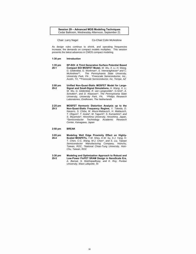
38
Session 29 – Advanced MOS Modeling Techniques Cedar Ballroom, Wednesday Afternoon, September 21
Chair: Larry Nagel Co-Chair:Colin McAndrew
As design rules continue to shrink, and operating frequencies increase, the demands on compact models multiplies. This session presents the latest advances in CMOS compact modeling. 1:30 pm Introduction 1:35 pm 29-1
SP-SOI: A Third Generation Surface Potential Based Compact SOI MOSFET Model, W. Wu, X. Li, H. Wang, G. Gildenblat, G. Workman*, S. Veeraraghavan* and C. McAndrew**, The Pennsylvania State University, University Park, PA , *Freescale Semiconductor, Inc., Austin, TX, **Freescale Semiconductor, Inc, Tempe, AZ
2:00 pm 29-2
Unified Non-Quasi-Static MOSFET Model for Large-Signal and Small-Signal Simulations, H. Wang, X. Li, W. Wu, G. Gildenblat, R. van Langevelde*, G.Smit*, A. Scholten*, and D. Klaassen*, The Pennsylvania State University, University Park, PA, *Philips Research Laboratories, Eindhoven, The Netherlands
2:25 pm 29-3
MOSFET Harmonic Distortion Analysis up to the Non-Quasi-Static Frequency Regime, Y. Takeda, D. Navarro, S. Chiba, M. Miura-Mattausch, H. Mattausch, T. Ohguro*, T. Iizuka*, M. Taguchi*, S. Kumashiro*, and S. Miyamoto*, Hiroshima University, Hiroshima, Japan, *Semiconductor Technology Academic Research Center, Kanagawa, Japan
2:50 pm BREAK 3:05 pm 29-4
Modeling Well Edge Proximity Effect on Highly-Scaled MOSFETs, Y-M. Sheu, K-W. Su, S-J. Yang, H-T. Chen, C-C. Wang, M-J. Chen*, and S. Liu, Taiwan Semiconductor Manufacturing Company, Hsinchu, Taiwan, ROC, *National Chiao-Tung University, Hsin-Chu, Taiwan, ROC
3:30 pm 29-5
Modeling and Optimization Approach to Robust and Low-Power FinFET SRAM Design in NanoScale Era, A. Bansal, S. Mukhopadhyay, and K. Roy, Purdue University, Wast Lafayette, IN
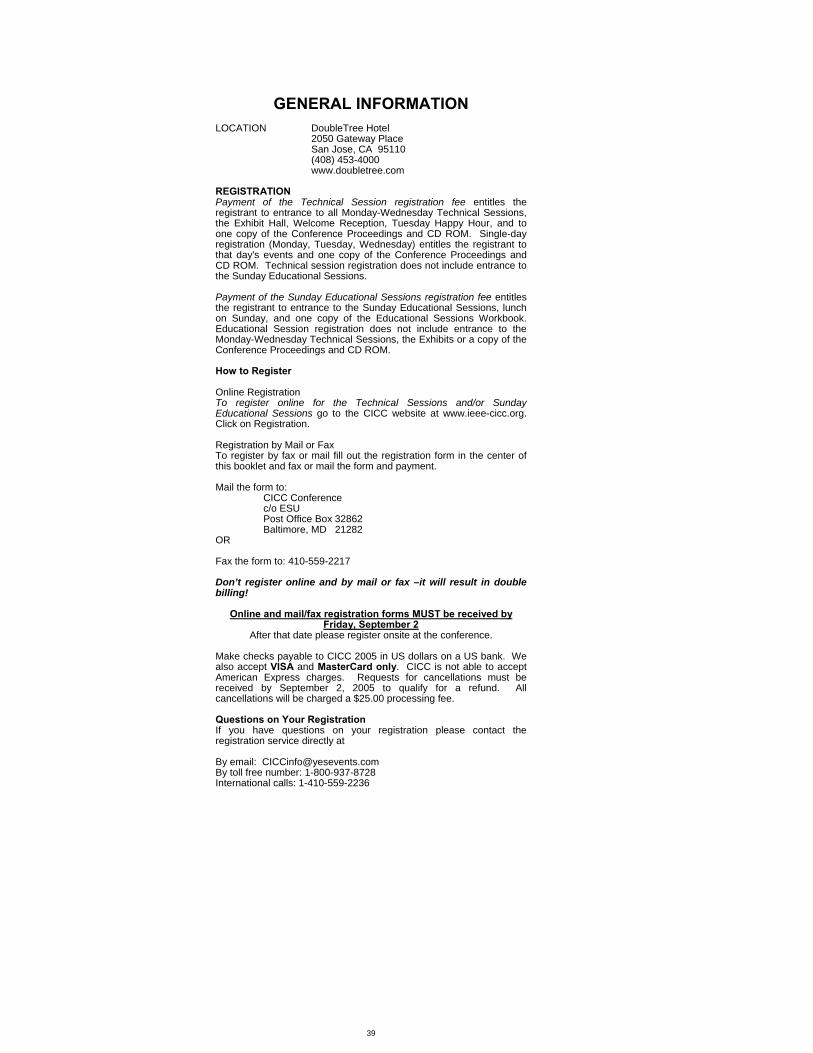
39
GENERAL INFORMATION LOCATION DoubleTree Hotel 2050 Gateway Place San Jose, CA 95110 (408) 453-4000 www.doubletree.com REGISTRATION Payment of the Technical Session registration fee entitles the registrant to entrance to all Monday-Wednesday Technical Sessions, the Exhibit Hall, Welcome Reception, Tuesday Happy Hour, and to one copy of the Conference Proceedings and CD ROM. Single-day registration (Monday, Tuesday, Wednesday) entitles the registrant to that day's events and one copy of the Conference Proceedings and CD ROM. Technical session registration does not include entrance to the Sunday Educational Sessions. Payment of the Sunday Educational Sessions registration fee entitles the registrant to entrance to the Sunday Educational Sessions, lunch on Sunday, and one copy of the Educational Sessions Workbook. Educational Session registration does not include entrance to the Monday-Wednesday Technical Sessions, the Exhibits or a copy of the Conference Proceedings and CD ROM. How to Register Online Registration To register online for the Technical Sessions and/or Sunday Educational Sessions go to the CICC website at www.ieee-cicc.org. Click on Registration. Registration by Mail or Fax To register by fax or mail fill out the registration form in the center of this booklet and fax or mail the form and payment. Mail the form to:
CICC Conference c/o ESU Post Office Box 32862 Baltimore, MD 21282
OR Fax the form to: 410-559-2217 Don’t register online and by mail or fax –it will result in double billing!
Online and mail/fax registration forms MUST be received by Friday, September 2
After that date please register onsite at the conference. Make checks payable to CICC 2005 in US dollars on a US bank. We also accept VISA and MasterCard only. CICC is not able to accept American Express charges. Requests for cancellations must be received by September 2, 2005 to qualify for a refund. All cancellations will be charged a $25.00 processing fee. Questions on Your Registration If you have questions on your registration please contact the registration service directly at By email: [email protected] By toll free number: 1-800-937-8728 International calls: 1-410-559-2236
40
Onsite Registration and Advance Registration Badge Pick-Up The Registration Center, located in the Bayshore Foyer, will be open as follows:
Registration for Sunday Educational Sessions Only
Sunday, Sept. 18 7:00 am - 2:00 pm Registration for Technical Sessions Sunday, Sept. 18 2:00 pm - 5:00 pm Monday, Sept. 19 7:30 am - 5:00 pm Tuesday, Sept. 20 8:00 am - 5:00 pm Wednesday, Sept. 21 8:00 am - 3:00 pm HOTEL ACCOMMODATIONS The DoubleTree Hotel is located at 2050 Gateway Place, San Jose, California. The hotel has an outdoor swimming pool and exercise facilities. Parking at the Hotel is free. The hotel is only 1 mile from the San Jose Airport. The room rate is $125 for a single or double room. All rooms must be guaranteed with a credit card. To make a hotel reservation call the hotel at (408) 453-4000 or go to the CICC website www.ieee-cicc.org , click on Hotel Reservations, then complete the form. The conference code for online reservations is CIC. The cut-off date for the CICC rate is August 26, 2005. To qualify for the CICC rate you MUST make your hotel reservation by the cut-off date. Make certain you tell reservations you are with IEEE CICC. You will receive a reservation confirmation directly from the hotel. It is the responsibility of each participant to make changes or cancellations directly with the hotel no later than 24 hours prior to scheduled arrival. No refunds will be given by the hotel for changes or cancellations with less than 24 hours notification. EDUCATIONAL SESSIONS On Sunday, Sept. 18, the CICC sponsors three Educational Sessions. These Sessions are:
1. Data Converter Design Techniques 2. Advanced RF: From Devices to Systems 3. High-Performance and Low-Power Digital Circuit Design
To register, complete the Advance Registration Form for receipt by Sept.2 WELCOME RECEPTION Monday Evening, Sept. 18, 5:30 pm - 8:00 pm Donner Pass Ballroom The CICC social event this year is the Welcome Reception sponsored by the CICC 2005 Exhibits Committee, held in the Exhibit Hall. All conference attendees are cordially invited! Enjoy the evening by browsing around the exhibit area, talking with the exhibitors' staff, seeing old friends and meeting new ones. CICC LUNCHEON Tuesday, Sept. 20, 12:00 pm - 1:30 pm Sierra Ballroom The CICC Luncheon features an address titled “Automotive Electronics: Steady Growth for Years to Come,” by Dr. Alberto Sangiovanni-Vincentelli, University of California, Berkeley. The luncheon is Tuesday, September 20, 12:00 noon – 1:30 pm. Luncheon is not included in the registration fee. Luncheon tickets are available through Advance Registration or onsite at a cost of $32 per ticket. See page 25 for a description of the presentation.

41
EVENING PANEL DISCUSSIONS On Tuesday evening, Sept. 20, beginning at 7:00 pm, the CICC will offer three evening panel discussions on timely issues: 1. Will Continued Process-Node Shrinks Kill High-Performance
Analog Design? 2. Foundries, EDA Vendors, and Designers: Who shoulders the
Blame When a Design Doesn’t Work in the Nano-Scale and Wireless Era?
3. Analog Behavioral Modeling: Fantasy, Fad, or Foundation for the Future?
CONFERENCE PROCEEDINGS The proceedings contains papers on each presentation. Technical Session registrants will receive one copy of the Proceedings. Additional copies will be available at the conference registration desk, IEEE member: $80, Non-member: $90. After the conference, order the Proceedings through: Single Copy Sales, IEEE Service Center, 445 Hoes Lane, Box 1331, Piscataway, NJ, 08855-1331, Customer Service Department (toll free): 800-678-4333. The IEEE catalogue number is 05CH37658 Approximately six weeks after the conference, technical session registrants will be mailed the conference CD ROM which includes copies of the papers and presentation slides. CICC gratefully acknowledges Philips Semiconductors’ sponsorship of this CD ROM. Additional copies of the CD ROM can be ordered onsite at the conference registration desk, IEEE member: $80, Non-member: $90. CD ROMs are not for sale by IEEE after the conference. AUTHOR INTERVIEWS There will be author interviews each day of the conference immediately following the afternoon sessions in Gateway Foyer. This additional forum provides an opportunity for relaxed discussions with your colleagues outside the strict time constrains of the regular sessions. SPONSOR EVENTS CICC acknowledges the generous support of our conference sponsors Philips Research for the CD ROM
AMI for the T-Shirts Cadence Design Systems for the Keynote Coffee Break Texas Instruments for the Internet Café Intel for the AV Sponsorship Altera for the AV Sponsorship Austriamicrosystems for the AV Sponsorship Emerging Memory Technologies for the AV Sponsorship AIRPORT TRANSPORTATION The DoubleTree Hotel is approximately 1 mile from San Jose Airport. There is a complementary hotel shuttle from San Jose Airport to the hotel that runs from 6:00 am to midnight. Call the hotel on the DoubleTree Courtesy Phone outside the baggage area at San Jose Airport. For passengers flying into San Francisco Airport, the San Jose Doubletree is approximately 33 miles from the airport. Supershuttle Service provides shuttle service from the airport to the hotel. Arrangements can be made at Ground Transportation or by calling (415) 558-8500 for more information. You can also make reservations online at www.supershuttle.com. The cost is $38.00/one way or $76.00/round-trip. Taxi service is also available from the airport at an estimated cost of $75.00.
42
BADGES Badges are required for admittance to all sessions and the exhibit hall. Please wear your badge at all times while attending the conference so that you will not be delayed entry to a session. FOR FURTHER INFORMATION CONTACT CICC 2005
Suite 312 16220 S. Frederick Ave. Gaithersburg, MD 20877 Phone: 301-527-0900 ext. 101, Fax: 301-527-0994 Email: [email protected] Home Page: http://www.ieee-cicc.org IEEE BMAS CONFERENCE This year the CICC is co-locating with the IEEE Behavior, Modeling, and Simulation Conference 2005. BMAS will take place September 22 – 23 at the DoubleTree Hotel, San Jose, California. Visit the BMAS website at www.bmas-conf.org for complete conference information.
Visit our website at www.ieee-cicc.org