Embed Size (px)
Citation preview
www.semtech.comPage 1
ADVANCED COMMUNICATIONS & SENSING USER GUIDE
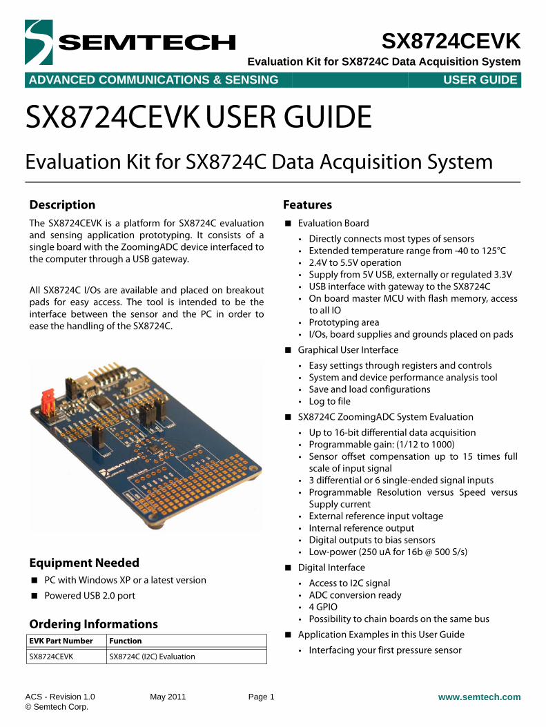
SX8724CEVKEvaluation Kit for SX8724C Data Acquisition System
ACS - Revision 1.0 May 2011© Semtech Corp.
SX8724CEVK USER GUIDEEvaluation Kit for SX8724C Data Acquisition System
DescriptionThe SX8724CEVK is a platform for SX8724C evaluationand sensing application prototyping. It consists of asingle board with the ZoomingADC device interfaced tothe computer through a USB gateway.
All SX8724C I/Os are available and placed on breakoutpads for easy access. The tool is intended to be theinterface between the sensor and the PC in order toease the handling of the SX8724C.
Equipment Needed PC with Windows XP or a latest version
Powered USB 2.0 port
Features Evaluation Board
• Directly connects most types of sensors• Extended temperature range from -40 to 125°C• 2.4V to 5.5V operation• Supply from 5V USB, externally or regulated 3.3V• USB interface with gateway to the SX8724C• On board master MCU with flash memory, access
to all IO• Prototyping area• I/Os, board supplies and grounds placed on pads
Graphical User Interface
• Easy settings through registers and controls• System and device performance analysis tool• Save and load configurations• Log to file
SX8724C ZoomingADC System Evaluation
• Up to 16-bit differential data acquisition• Programmable gain: (1/12 to 1000)• Sensor offset compensation up to 15 times full
scale of input signal• 3 differential or 6 single-ended signal inputs• Programmable Resolution versus Speed versus
Supply current• External reference input voltage• Internal reference output• Digital outputs to bias sensors• Low-power (250 uA for 16b @ 500 S/s)
Digital Interface
• Access to I2C signal• ADC conversion ready• 4 GPIO• Possibility to chain boards on the same bus
Application Examples in this User Guide
• Interfacing your first pressure sensor
Ordering InformationsEVK Part Number Function
SX8724CEVK SX8724C (I2C) Evaluation

ACS - Revision 1.0 May 2011© Semtech Corp.
www.semtech.comPage 2
Section Page
TABLE OF CONTENT ADVANCED COMMUNICATIONS & SENSING USER GUIDE
SX8724CEVKEvaluation Kit for SX8724C Data Acquisition System
GETTING STARTED . . . . . . . . . . . . . . . . . . . . . . . . . . . . . . . . . . . . . . . . . . . . . . . . . . . . . . . . . . . . . . 4
1 Introduction. . . . . . . . . . . . . . . . . . . . . . . . . . . . . . . . . . . . . . . . . . . . . . . . . . . . . . . . . . . . . . . . . . . . . . . . . . . 42 Evaluation Kit Contents . . . . . . . . . . . . . . . . . . . . . . . . . . . . . . . . . . . . . . . . . . . . . . . . . . . . . . . . . . . . . . . . . 43 Board Overview . . . . . . . . . . . . . . . . . . . . . . . . . . . . . . . . . . . . . . . . . . . . . . . . . . . . . . . . . . . . . . . . . . . . . . . 54 Software Installation . . . . . . . . . . . . . . . . . . . . . . . . . . . . . . . . . . . . . . . . . . . . . . . . . . . . . . . . . . . . . . . . . . . . 64.1 About Microsoft .NET Framework . . . . . . . . . . . . . . . . . . . . . . . . . . . . . . . . . . . . . . . . . . . . . . . . . . . . . . . . 75 Board Connection and Drivers Installation (first time) . . . . . . . . . . . . . . . . . . . . . . . . . . . . . . . . . . . . . . . . . . 8
HARDWARE DESCRIPTION . . . . . . . . . . . . . . . . . . . . . . . . . . . . . . . . . . . . . . . . . . . . . . . . . . . . . . . . . 9
6 Board Schematic . . . . . . . . . . . . . . . . . . . . . . . . . . . . . . . . . . . . . . . . . . . . . . . . . . . . . . . . . . . . . . . . . . . . . . 97 User Interfaces . . . . . . . . . . . . . . . . . . . . . . . . . . . . . . . . . . . . . . . . . . . . . . . . . . . . . . . . . . . . . . . . . . . . . . . 107.1 Prototyping Area . . . . . . . . . . . . . . . . . . . . . . . . . . . . . . . . . . . . . . . . . . . . . . . . . . . . . . . . . . . . . . . . . . . . 118 Power Supply . . . . . . . . . . . . . . . . . . . . . . . . . . . . . . . . . . . . . . . . . . . . . . . . . . . . . . . . . . . . . . . . . . . . . . . . 128.1 Power Sources Specifications. . . . . . . . . . . . . . . . . . . . . . . . . . . . . . . . . . . . . . . . . . . . . . . . . . . . . . . . . . 128.2 Power Supply Selection . . . . . . . . . . . . . . . . . . . . . . . . . . . . . . . . . . . . . . . . . . . . . . . . . . . . . . . . . . . . . . 139 USB Interface . . . . . . . . . . . . . . . . . . . . . . . . . . . . . . . . . . . . . . . . . . . . . . . . . . . . . . . . . . . . . . . . . . . . . . . . 149.1 Gateway to SX8724C . . . . . . . . . . . . . . . . . . . . . . . . . . . . . . . . . . . . . . . . . . . . . . . . . . . . . . . . . . . . . . . . 1410 EVK Bill of Materials List . . . . . . . . . . . . . . . . . . . . . . . . . . . . . . . . . . . . . . . . . . . . . . . . . . . . . . . . . . . . . . . 1611 Board Physical Dimensions . . . . . . . . . . . . . . . . . . . . . . . . . . . . . . . . . . . . . . . . . . . . . . . . . . . . . . . . . . . . . 1811.1 Errata Note . . . . . . . . . . . . . . . . . . . . . . . . . . . . . . . . . . . . . . . . . . . . . . . . . . . . . . . . . . . . . . . . . . . . . . . . 18
GRAPHICAL USER INTERFACE . . . . . . . . . . . . . . . . . . . . . . . . . . . . . . . . . . . . . . . . . . . . . . . . . . . . . 19
12 Software Tool Overview . . . . . . . . . . . . . . . . . . . . . . . . . . . . . . . . . . . . . . . . . . . . . . . . . . . . . . . . . . . . . . . . 1913 Main Window . . . . . . . . . . . . . . . . . . . . . . . . . . . . . . . . . . . . . . . . . . . . . . . . . . . . . . . . . . . . . . . . . . . . . . . . 2013.1 Menu Tool Bar. . . . . . . . . . . . . . . . . . . . . . . . . . . . . . . . . . . . . . . . . . . . . . . . . . . . . . . . . . . . . . . . . . . . . . 2013.2 Window Tool Bar. . . . . . . . . . . . . . . . . . . . . . . . . . . . . . . . . . . . . . . . . . . . . . . . . . . . . . . . . . . . . . . . . . . . 2213.3 Status Bar . . . . . . . . . . . . . . . . . . . . . . . . . . . . . . . . . . . . . . . . . . . . . . . . . . . . . . . . . . . . . . . . . . . . . . . . . 2313.4 ZoomingADC controls . . . . . . . . . . . . . . . . . . . . . . . . . . . . . . . . . . . . . . . . . . . . . . . . . . . . . . . . . . . . . . . . 2413.5 Voltage Control . . . . . . . . . . . . . . . . . . . . . . . . . . . . . . . . . . . . . . . . . . . . . . . . . . . . . . . . . . . . . . . . . . . . . 2813.6 Estimated Device Performances. . . . . . . . . . . . . . . . . . . . . . . . . . . . . . . . . . . . . . . . . . . . . . . . . . . . . . . . 2813.7 Display Chart. . . . . . . . . . . . . . . . . . . . . . . . . . . . . . . . . . . . . . . . . . . . . . . . . . . . . . . . . . . . . . . . . . . . . . . 3013.8 Log Data to File. . . . . . . . . . . . . . . . . . . . . . . . . . . . . . . . . . . . . . . . . . . . . . . . . . . . . . . . . . . . . . . . . . . . . 3114 ZoomingADC Data Display Window. . . . . . . . . . . . . . . . . . . . . . . . . . . . . . . . . . . . . . . . . . . . . . . . . . . . . . . 3214.1 ZoomingADC data display panel. . . . . . . . . . . . . . . . . . . . . . . . . . . . . . . . . . . . . . . . . . . . . . . . . . . . . . . . 3214.2 Histogram Panel - Noise Analysis. . . . . . . . . . . . . . . . . . . . . . . . . . . . . . . . . . . . . . . . . . . . . . . . . . . . . . . 3314.3 Measured System Performances . . . . . . . . . . . . . . . . . . . . . . . . . . . . . . . . . . . . . . . . . . . . . . . . . . . . . . . 3315 Registers Display Window . . . . . . . . . . . . . . . . . . . . . . . . . . . . . . . . . . . . . . . . . . . . . . . . . . . . . . . . . . . . . . 3516 Verification Mode Window . . . . . . . . . . . . . . . . . . . . . . . . . . . . . . . . . . . . . . . . . . . . . . . . . . . . . . . . . . . . . . 35
APPLICATION EXAMPLES . . . . . . . . . . . . . . . . . . . . . . . . . . . . . . . . . . . . . . . . . . . . . . . . . . . . . . . . . 36
17 Interfacing your first pressure sensor . . . . . . . . . . . . . . . . . . . . . . . . . . . . . . . . . . . . . . . . . . . . . . . . . . . . . . 3617.1 Introduction . . . . . . . . . . . . . . . . . . . . . . . . . . . . . . . . . . . . . . . . . . . . . . . . . . . . . . . . . . . . . . . . . . . . . . . . 3617.2 Pressure Sensor . . . . . . . . . . . . . . . . . . . . . . . . . . . . . . . . . . . . . . . . . . . . . . . . . . . . . . . . . . . . . . . . . . . . 3617.3 Using the Evaluation Board and the GUI . . . . . . . . . . . . . . . . . . . . . . . . . . . . . . . . . . . . . . . . . . . . . . . . . 40
ACS - Revision 1.0 May 2011© Semtech Corp.
www.semtech.comPage 3
Section Page
TABLE OF CONTENT ADVANCED COMMUNICATIONS & SENSING USER GUIDE
SX8724CEVKEvaluation Kit for SX8724C Data Acquisition System
17.4 Reading the sensor using the GUI . . . . . . . . . . . . . . . . . . . . . . . . . . . . . . . . . . . . . . . . . . . . . . . . . . . . . . 4117.5 Reference Voltage Selection. . . . . . . . . . . . . . . . . . . . . . . . . . . . . . . . . . . . . . . . . . . . . . . . . . . . . . . . . . . 4117.6 ZoomingADC™ Configuration. . . . . . . . . . . . . . . . . . . . . . . . . . . . . . . . . . . . . . . . . . . . . . . . . . . . . . . . . . 4317.7 ADC Configuration . . . . . . . . . . . . . . . . . . . . . . . . . . . . . . . . . . . . . . . . . . . . . . . . . . . . . . . . . . . . . . . . . . 4617.8 Noise Cancellation . . . . . . . . . . . . . . . . . . . . . . . . . . . . . . . . . . . . . . . . . . . . . . . . . . . . . . . . . . . . . . . . . . 4817.9 LSB Equivalence. . . . . . . . . . . . . . . . . . . . . . . . . . . . . . . . . . . . . . . . . . . . . . . . . . . . . . . . . . . . . . . . . . . . 4917.10 ZoomingADC™ Benefits . . . . . . . . . . . . . . . . . . . . . . . . . . . . . . . . . . . . . . . . . . . . . . . . . . . . . . . . . . . . . . 50

www.semtech.comPage 4
ADVANCED COMMUNICATIONS & SENSING USER GUIDE
SX8724CEVKEvaluation Kit for SX8724C Data Acquisition System
ACS - Revision 1.0 May 2011© Semtech Corp.
GETTING STARTED
1 IntroductionThis section describes a typical configuration for operating the evaluation board of the SX8724C withZoomingADC.
The SX8724C is a signal conditioner based on Semtech's ultra low power ZoomingADC™ technology. Itdirectly connects most types of miniature sensors with a general purpose microcontroller.
The SX8724CEVK is a USB based evaluation tool designed to allow simple and easy evaluation of thesuitability of the SX8724C device for a given application.
The analog input signal can be entered either in differential or single ended. Refer to the datasheet for theimpact of driving an analog input in single or in differential.
2 Evaluation Kit ContentsThe SX8724CEVK evaluation kit consists of:
a “Read me first” sheet
an Evaluation Board
one USB cable
a CDROM containing:
• Software Installer including MS .NET framework 3.5 and USB drivers• SX8724CEVK User Guide (this document)

www.semtech.comPage 5
ADVANCED COMMUNICATIONS & SENSING USER GUIDE
SX8724CEVKEvaluation Kit for SX8724C Data Acquisition System
ACS - Revision 1.0 May 2011© Semtech Corp.
3 Board Overview
The picture below describes the main zones and functions accessible on theSX8724CEVK
Figure 1. SX8724CEVK Board Overview
USB Gateway Interface
Isolate/connect device
Analog Interface
Prototyping Area
Acquisition Device
& Power Management
& Digital Interface

www.semtech.comPage 6
ADVANCED COMMUNICATIONS & SENSING USER GUIDE
SX8724CEVKEvaluation Kit for SX8724C Data Acquisition System
ACS - Revision 1.0 May 2011© Semtech Corp.
4 Software InstallationIf the evaluation kit is supplied with an insert sheet, follow the instruction on the insert sheet. The latestsoftware revision can be downloaded on Semtech website.
1. Put the CDROM in your computer and browse the contents of the CD, open the SX8724xEvaluationKitSetup.exe file manually. It can be found in the root of the CD-ROM. Click on Next> to start the installation
Figure 2. Installation Screen

www.semtech.comPage 7
ADVANCED COMMUNICATIONS & SENSING USER GUIDE
SX8724CEVKEvaluation Kit for SX8724C Data Acquisition System
ACS - Revision 1.0 May 2011© Semtech Corp.
2. Choose the installation directory. The software must be installed on a local directory. Click on Next> to confirm the path.
3. Follow the on-screen installation guidelines until the process is completed. Please note that .NETFramework 3.5 and the PIC USB driver will be automatically installed if not detected on your computer.(Administrator rights may be needed).
4. The GUI software and .Net Framework are now installed on your computer.
4.1 About Microsoft .NET FrameworkThe Microsoft .NET Framework 3.5 is required to run the software. The software installer will install the itautomatically if not present on your computer.
Details and installation information about the .NET Framework are available on Microsoft web site (http://www.microsoft.com). Then go to the Download section.
There are multiple versions of the .NET Framework available from Microsoft, and they can be installed side-by-side on the same computer. Contact your system administrator for more details.
Figure 3. Software Install Location

www.semtech.comPage 8
ADVANCED COMMUNICATIONS & SENSING USER GUIDE
SX8724CEVKEvaluation Kit for SX8724C Data Acquisition System
ACS - Revision 1.0 May 2011© Semtech Corp.
5 Board Connection and Drivers Installation (first time)
1. Connect the board to the PC with the USB interface. The board is powered via the USB and will be detected as new USB peripheral. Choose the “Install the software automatically (Recommended)” option and click on the Next> button.
2. Windows will search for the associated driver and install the board as new peripheral.
3. Follow the on-screen installation guidelines until the process is completed. Driver compatibility screens may appear during the installation procedure. Validate always by clicking the “Continue Anyway button”:
4. The drivers are now installed. The board and its dedicated software are ready to be used. Launch SX8724xEVK software from the Windows Start menu.
www.semtech.comPage 9
ADVANCED COMMUNICATIONS & SENSING USER GUIDE
SX8724CEVKEvaluation Kit for SX8724C Data Acquisition System
ACS - Revision 1.0 May 2011© Semtech Corp.
HARDWARE DESCRIPTION
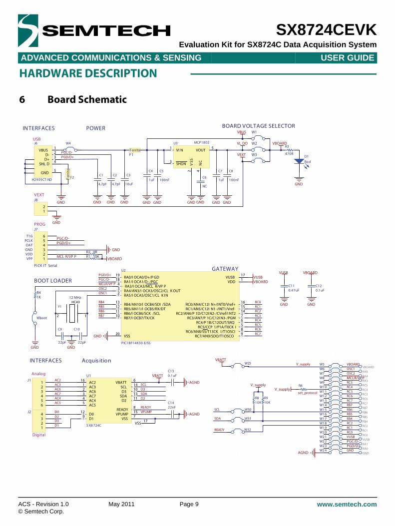
6 Board Schematic
SDA
SCL
GND
D3
READY
VBOARDVUSB
12
J8
GND
123456
J1 AGND
0.1uFC13
RB6
RB4
RC7
Ferr
ite
F2
VBUS 1
D- 2
D+ 3
GND 5
SHL D 4
J6
H2959CT-ND
FerriteF1
10uF
C3
NC
C61uF
C7
100nF
C8
1uF
C4
100nF
C5
D1Red
470R
R3
SHDN3
NC
4
VSS
2
VOUT 5VI N1U3 MCP1802
C1 C2
VL DO
OSC2OSC1
W2
W3
RC5RC4RC3RC2RC1RC0
RB5
RB7
W1
AGND
VBUS
VBOARD
PGD/D+PGC/D-
PGD/D+PGC/D-
VBATT
MCLR/VP P
1234J2 VPUMP
D2
RC6
VDD 1
RA5/I OCA5/OSC1/CL K IN2 RA4/AN3/I OCA3/OSC2/CL K OUT3 RA3/I OCA3/MCL R/VP P4
RC5/CCP 1/P1A/T0CK I 5RC4/P 1B/C12OUT/SRQ 6RC3/AN7/P 1C/C12I N3-/PGM 7
RC6/AN8/SS/T13CK I/T1OSCI 8
RC7/AN9/SDO/T1OSCO 9
RB7/I OCB7/TX/CK10 RB6/I OCB6/SCK /SCL11 RB5/AN11/I OCB5/RX/DT12 RB4/AN10/I OCB4/SDI /SDA13
RC2/AN6/P 1D/C12I N2-/CVref/I NT2 14RC1/AN5/C12I N1-/INT1/Vref- 15RC0/AN4/C12I N+/INT0/Vref+ 16
VUSB 17
RA1/I OCA1/D- /PGC18 RA0/I OCA0/D+/P GD19
VSS20
U2
PIC18F14K50-E/SS
Analog
POWER
Digital
D3
VEXT
USB
INTERFACES
Acquis ition
GATEWAY
2 1
HC49Y1
22pF
C9
22pF
C10
GND
12 MHz
123456
J7
PICK IT Serial
10KR1
GND0RR2
VPPVDDGNDDAT
PCLKT1G
PGC/D-
VBOARD
PGD/D+
MCL R/VP P
VEXT
22nFC14
PROG
GNDGNDGNDGNDGNDGNDGNDGNDGNDGND
GND
W32READY
W25
10KR8
10KR9
W30
W31
SCL
V_supply
VBATT
SDA
BOARD VOLTAGE SELECTOR
W17W18W19W20W21W22W23W24
GND
VBOARDVUSB
0.47uFC11
0.1uFC12
GND
RB6
RB4RB5
RC2RC1RC0
W5W6W7W8W9W10W11W12W13W14W15W16
VBOARD
RC5RC4RC3RC6RC7RB7
VUSB
W4
AGND
INTERFACES
PGC/D-PGD/D+
MCLR/VPPOSC2OSC1
V_supply
D2
AC2AC3
AC4AC5
AC6AC7
D0
D1
AC31
AC44
AC55
AC62
AC73
VBATT 6
VSS 7
READY 8
D19
D3 10
D2 11
D012
SDA 13
SCL 14
VPUMP 15
AC216
VSS 17
U1
S X8 724C
R6
set_protocolV_supply
VBOARDRA5RA4RA3RC5RC4RC3RC6RC7RB7RB6RB5RB4RC2RC1RC0VUSBRA1RA0GND
GND
BOOT LOADER
Wboot
1KR4
GND
4.7pF 4.7pF

www.semtech.comPage 10
ADVANCED COMMUNICATIONS & SENSING USER GUIDE
SX8724CEVKEvaluation Kit for SX8724C Data Acquisition System
ACS - Revision 1.0 May 2011© Semtech Corp.
7 User InterfacesThe analog interface gives access to the ZoomingADC inputs. The digital interface gives access to the GPIOpins, the PC gateway connections and the power supplies. The analog and digital connections are availableon single row 2.54mm connectors and on the bare PCB next to the prototyping area.
The connections points are available for industrial PCB terminal blocks and on the bare PCB next to theSX8724C
Figure 4. Analog Interface Schematic
Figure 5. SX8724C Interface on the Board
SDA
SCLD3
READY
123456
J1 AGND
0.1uFC13
AGND
VBATT
1234J2 VPUMP
D2
Analog
Digital
D3
Acquis ition
22nFC14
INTERFACES
D2
AC2AC3
AC4AC5
AC6AC7
D0
D1
AC31
AC44
AC55
AC62
AC73
VBATT 6
VSS 7
READY 8
D19
D3 10
D2 11
D012
SDA 13
SCL 14
VPUMP 15
AC216
VSS 17
U1
S X8 724C
4
Analog interface Digital interface+ Vref,in and Vref,out
Connect SX8724CVBATT pin to supply(or measure current)
Connect SX8724C READYsignal to gateway
Connect I2C interface to SX8724C(pull-ups are on gateway side)
C
pcb_e204v02a

www.semtech.comPage 11
ADVANCED COMMUNICATIONS & SENSING USER GUIDE
SX8724CEVKEvaluation Kit for SX8724C Data Acquisition System
ACS - Revision 1.0 May 2011© Semtech Corp.
7.1 Prototyping AreaUsing the prototyping area, one can set its own application only using the SX8724C and bypassing theonboard gateway.
Figure 6. Prototyping Area

www.semtech.comPage 12
ADVANCED COMMUNICATIONS & SENSING USER GUIDE
SX8724CEVKEvaluation Kit for SX8724C Data Acquisition System
ACS - Revision 1.0 May 2011© Semtech Corp.
8 Power SupplyThe board provides different power supply voltage possibilities; the following paragraphs describe how toconfigure and use them.
8.1 Power Sources SpecificationsThe board can be powered through three different sources:
1. VBUS: USB power coming from the PC.2. VLDO: 3.3V Regulated voltage.3. VEXT: External source applied on VEXT interface.
Input analog voltages specified in the device datasheet.
Table 1. Power Sources Specifications
Voltage range Min Typ Max Unit Comment
VBUS 4.5 5 5.5 V DC, Unregulated
VLDO1
1. Temperature range from -40 to 85°C
3.3 V DC, Regulated
VEXT 2.4 - 5.5 V DC, Unregulated 2
2. External power supply
Board current driving capability
- 100 mA
www.semtech.comPage 13
ADVANCED COMMUNICATIONS & SENSING USER GUIDE
SX8724CEVKEvaluation Kit for SX8724C Data Acquisition System
ACS - Revision 1.0 May 2011© Semtech Corp.
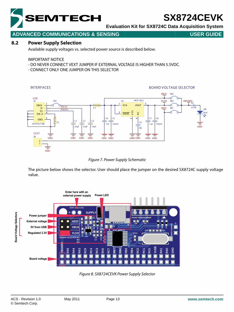
8.2 Power Supply SelectionAvailable supply voltages vs. selected power source is described below.
IMPORTANT NOTICE- DO NEVER CONNECT VEXT JUMPER IF EXTERNAL VOLTAGE IS HIGHER THAN 5.5VDC.- CONNECT ONLY ONE JUMPER ON THIS SELECTOR
The picture below shows the selector. User should place the jumper on the desired SX8724C supply voltagevalue.
Figure 7. Power Supply Schematic
Figure 8. SX8724CEVK Power Supply Selector
12
J8
GND
Ferr
ite
F2
VBUS 1
D- 2
D+ 3
GND 5
SHL D 4
J6
H2959CT-ND
FerriteF1
10uF
C3
NC
C61uF
C7
100nF
C8
1uF
C4
100nF
C5
ONRed
470R
R3
SHDN3
NC
4
VSS
2
VOUT 5VI N1U3 MCP1802
27pF
C1
27pF
C2
VLDO W3
W1
W2VBUS
VBOARD
PGD/D+PGC/D-
VEXT
USB
INTERFACES
VEXT
GNDGNDGNDGNDGNDGNDGNDGNDGNDGND
GND
BOARD VOLTAGE SELECTOR
W4
Power jumper
Power LED Enter here with an external power supply
External voltage
5V from USB
Regulated 3.3V
Board voltage
Boar
d Vo
ltage
Sel
ecto
rs

www.semtech.comPage 14
ADVANCED COMMUNICATIONS & SENSING USER GUIDE
SX8724CEVKEvaluation Kit for SX8724C Data Acquisition System
ACS - Revision 1.0 May 2011© Semtech Corp.
9 USB Interface9.1 Gateway to SX8724C
The USB gateway is a complete interface to drive the SX8724C on the board. The knowledge, implementationor modification of this gateway is not required for evaluation.This interface is used to communicate with the GUI, but can also enable automation with external processessuch as Python, MATLAB, and LabVIEW.
Figure 9. PIC Gateway Schematic
Figure 10. PIC Gateway on the Board
GND
VBOARDVUSB
RB6
RB4
RC7
OSC2OSC1
RC5RC4RC3RC2RC1RC0
RB5
RB7
PGD/D+PGC/D-MCLR/VPP
RC6
VDD 1
RA5/I OCA5/OSC1/CL K IN2 RA4/AN3/I OCA3/OSC2/CL K OUT3 RA3/I OCA3/MCL R/VP P4
RC5/CCP 1/P1A/T0CK I 5RC4/P 1B/C12OUT/SRQ 6RC3/AN7/P 1C/C12I N3-/PGM 7
RC6/AN8/SS/T13CK I/T1OSCI 8
RC7/AN9/SDO/T1OSCO 9
RB7/I OCB7/TX/CK10 RB6/I OCB6/SCK /SCL11 RB5/AN11/I OCB5/RX/DT12 RB4/AN10/I OCB4/SDI /SDA13
RC2/AN6/P 1D/C12I N2-/CVref/I NT2 14RC1/AN5/C12I N1-/INT1/Vref- 15RC0/AN4/C12I N+/INT0/Vref+ 16
VUSB 17
RA1/I OCA1/D- /PGC18 RA0/I OCA0/D+/P GD19
VSS20
U2
PIC18F14K50-E/SS
2 1
HC49Y1
22pF
C9
22pF
C10
GND
12 MHz
GND
VUSB
0.47uFC11
0.1uFC12
GND
BOOT LOADER J9
1KR4
GND
VBOARD
PICKit programmer/debugger interface
Bootloader mode control
PIC gateway
Pin access to the PIC gateway
USB interface

www.semtech.comPage 15
ADVANCED COMMUNICATIONS & SENSING USER GUIDE
SX8724CEVKEvaluation Kit for SX8724C Data Acquisition System
ACS - Revision 1.0 May 2011© Semtech Corp.
9.1.1 Bootloader ModeThe BOOT LOADER (J9) jumper allows the user to set the onboard PIC18F14K50 in bootloader mode and toprogram it. One can then update the gateway with the latest driver from Semtech website or set its ownsolution1 using the I2C interface (see 7.1. Prototyping Area).By default, the jumper is not connected.To enter in bootloader mode, shortcut the BOOT LOADER (J9) jumper and restart the PIC by unplug-plug theSUPPLY jumper or disconnect-connect the USB cable (see Figure 10 on page 14).
9.1.2 PICkit Programming InterfaceThis interface is used to program the board with a Microchip PICkit 3 Programmer/Debugger.
1. Semtech does not provide support for modified Gateway software other than the official releases available on the website.
Figure 11. PICKIT Programmer Interface
123456
J7
PICK IT Serial
10KR1
GND0RR2
VPPVDDGND
ICSPDATICSPCLK
T1GPGC/D-
VBOARD
PGD/D+
MCL R/VP P
PROG

www.semtech.comPage 16
ADVANCED COMMUNICATIONS & SENSING USER GUIDE
SX8724CEVKEvaluation Kit for SX8724C Data Acquisition System
ACS - Revision 1.0 May 2011© Semtech Corp.
10 EVK Bill of Materials List
Table 2. SX8724CEVK Bill of Material
Ref Val Package Description Manufacturer Part#
IC
U1 MLPQ-16 4x4 SX8724C acquisition system SEMTECH SX8724CWLTDT
U2 SSOP-20, 6.5mm pitch PIC Gateway Microchip PIC18F14K50-E/SS
U3 SOT23-5 3.3V REG LDO 300MA Microchip MCP1802T-3302I/OT
Connectors
J6Surface Mount, Right Angle, Horizontal
Connector mini USB2.0 Interconnects UX60-MB-5ST
J7 Through Hole, Right AngleHeader BRKWAY .100 6POS R/A
Tyco Electronics 9-103325-0-06
Crystal
Y1 Surface Mount, HC49/USCrystal 12.00000 MHZ18pF SMD
Abracon Corporation ABLS-12.000MHZ-K4T
Jumpers/selectors
W1, W2, W3,
Through Hole, 2.54mm3x2 header + 1x RED jumper
W4, W25,W32
Through Hole, 2.54mm3x 1x2 headers+ 3x BLACK jumper
W30, W31
Through Hole, 2.54mm2x2 header+ 2x BLACK jumper
Ferrites Bead
F1, F2 SMD 0805 Ferrite 1.5A 40 Ohm Steward PZ2012D400-3R0TF
Resistors
R1, R5, R6
10K SMD 0603
R2 0R SMD 0603 PICKIT prog
R3 470R SMD 0603 LED current limiting resistor
R4 1K SMD 0603Protection for Bootloader bypass
Capacitors
C1, C2,
47pF SMD 0603
C3 10uF SMD 0805
C4, C7
1uF SMD 0603

www.semtech.comPage 17
ADVANCED COMMUNICATIONS & SENSING USER GUIDE
SX8724CEVKEvaluation Kit for SX8724C Data Acquisition System
ACS - Revision 1.0 May 2011© Semtech Corp.
C5, C8, C12, C13
100nF SMD 0603
C9, C10
22pF SMD 0603
C11 47nF SMD 0603
C14 22nF SMD 0603
Table 2. SX8724CEVK Bill of Material
Ref Val Package Description Manufacturer Part#

www.semtech.comPage 18
ADVANCED COMMUNICATIONS & SENSING USER GUIDE
SX8724CEVKEvaluation Kit for SX8724C Data Acquisition System
ACS - Revision 1.0 May 2011© Semtech Corp.
11 Board Physical Dimensions
11.1 Errata NoteBoards with the PCB reference pcb_e204v02a have the MOSI and SCLK marking inverted.
Figure 12. SX8724CEVK Board Overview
4C

www.semtech.comPage 19
ADVANCED COMMUNICATIONS & SENSING USER GUIDE
SX8724CEVKEvaluation Kit for SX8724C Data Acquisition System
ACS - Revision 1.0 May 2011© Semtech Corp.
GRAPHICAL USER INTERFACE
12 Software Tool OverviewThe SX8724CEVK includes a graphical user interface (GUI) that provides simplified access to all key registerson the board. It uses intuitive controls and popup menus to write settings from the hardware.This GUI takes high level input from the user and computes the required low level register values. With theGUI, the user is not required to compute complicated equations to determine which values must be writtenfor board operation. In addition, the GUI simplifies analog interfacing by providing controls that simplifyalignment of analog functions.The figure below illustrates the SX8724xEVK graphical user interface (GUI). Each of the numbered captionscorresponds to a proceeding chapter within the sections which correspond to the description of that GUI feature:
1. see section 13.1. Menu Tool Bar in page 202. see section 13.2. Window Tool Bar in page 223. see section 13.3. Status Bar in page 234. see section 13.4. ZoomingADC controls in page 245. see section 13.4.5. General Controls in page 256. see section 13.5. Voltage Control in page 287. see section 13.6. Estimated Device Performances in page 288. see section 13.7. Display Chart in page 30
Figure 13. SX872xEVK GUI Overview
4.
5.
7.
6.
8.
1.2.
3.

www.semtech.comPage 20
ADVANCED COMMUNICATIONS & SENSING USER GUIDE
SX8724CEVKEvaluation Kit for SX8724C Data Acquisition System
ACS - Revision 1.0 May 2011© Semtech Corp.
13 Main Window13.1 Menu Tool Bar
The Menu tool bar contains four drop down menus, File Menu, Action Menu, Tools Menu and Help Menu.
13.1.1 File Menu Connect / Disconnect allows the connection or disconnection of the board from the host PC. This functionality can also be accessed through the short cut buttons of the Window Toolbar (see 13.2. Window Tool Bar).
Open Config… allows for the opening of SX8724xEVK configuration files (.cfg). This is implemented through a standard Windows file dialog box and may also be accessed through the short cut buttons of the Window Toolbar.
Save Config allows for SX8724xEVK configuration files (.cfg) to be saved. This is implemented through a standard Windows file dialog box. The default file name is the last saved configuration file.
Save Config as… prompts for a new file name before saving, allowing for multiple configuration files to be saved and may also be accessed through the short cut buttons of the Window Toolbar.
Exit closes the application.
13.1.2 Action Menu Reset resets the SX8724C configuration registers to the default valuesby sending an I2C General Call Reset command.
Refresh reads all SX8724C registers and updates the GUI controls.
Show registers toggles the SX8724C Registers display window and may also be accessed through the short cut buttons of the Window Toolbar. The register display window indicates the status of SX8724C
Figure 14. File Menu Options

www.semtech.comPage 21
ADVANCED COMMUNICATIONS & SENSING USER GUIDE
SX8724CEVKEvaluation Kit for SX8724C Data Acquisition System
ACS - Revision 1.0 May 2011© Semtech Corp.
configuration registers as detailed in the SX8724C datasheet. Refer to 15. Registers Display Window section for further information.
13.1.3 Help Menu Help opens a HTML help window with GUI controls descriptions.
User's Guide… opens a PDF version of the User Guide.
About… provides details of the GUI revision. The latest version of the GUI can be downloaded from Semtech web site.
Figure 15. Action Menu Options
Figure 16. Help Menu Options

www.semtech.comPage 22
ADVANCED COMMUNICATIONS & SENSING USER GUIDE
SX8724CEVKEvaluation Kit for SX8724C Data Acquisition System
ACS - Revision 1.0 May 2011© Semtech Corp.
13.2 Window Tool BarThe Windows Tool Bar contains buttons that provide shortcuts to some of the functions accessed from thedrop-down menus.
Open Config, USB Connect / Disconnect and Save Config buttons provides a direct control of the actions described in 13.1.1. File Menu section. A configuration file illustrated below in Figure 18.
Reset, Refresh and Show registers provides a direct control of the actions described in 13.1.2. Action Menu
I2C address button set the I2C device address that the GUI will access.
Help button provides a direct control of the actions described in 13.1.3. Help Menu.
Figure 17. Windows Tool Bar Menu
Figure 18. Example Configuration File Text Editor Output

www.semtech.comPage 23
ADVANCED COMMUNICATIONS & SENSING USER GUIDE
SX8724CEVKEvaluation Kit for SX8724C Data Acquisition System
ACS - Revision 1.0 May 2011© Semtech Corp.
13.3 Status BarThe Status Bar provides error messages, the onboard SX8724C version and the current user configuration file.For further information concerning the IC revision, please refer to the SX8724C datasheet.
Figure 19. Status Bar
Message IC Revision Number Configuration File

www.semtech.comPage 24
ADVANCED COMMUNICATIONS & SENSING USER GUIDE
SX8724CEVKEvaluation Kit for SX8724C Data Acquisition System
ACS - Revision 1.0 May 2011© Semtech Corp.
13.4 ZoomingADC controlsThe ZoomingADC control sections allows the user to configure the acquisition chain of the SX8724C byselecting the control corresponding to the desired mode. Note that the settings are applied to the deviceregisters as soon as the control is changed.
The representation picture on the top gives an indication of the settings applied to the ZoomingADC.
13.4.1 Reference selection controlThis control allows to choose the reference voltage of the acquisition chain. This can be the internallygenerated VREF with a nominal value of 1.22V or VBATT (2.4V to 5.5V).
When the control selects VREF, it can also be selected combined with a GPIO to provide a reference voltagefrom GPIO. See Section 13.4.7 for details.
13.4.2 Inputs controlsThe controls in the group named “Inputs” lets the user choose which inputs and which reference pins will beused to make the measurement. On this group of controls the user may also choose if the inputs are “Single-ended” or “Differential” as well as choosing which of the inputs is used as “Positive” or “Negative” input.
13.4.3 PGA controlsThe group of controls named “PGA” lets the user control the gain, offset and enabling disabling each PGAindividually.
The user has also the possibility to control the PGAs biasing current ratio.
Figure 20. ZoomingADC Control Sections

www.semtech.comPage 25
ADVANCED COMMUNICATIONS & SENSING USER GUIDE
SX8724CEVKEvaluation Kit for SX8724C Data Acquisition System
ACS - Revision 1.0 May 2011© Semtech Corp.
13.4.4 ADC controlsThe group of controls named “ADC” lets the user control the ADC parameters. Parameters like number ofelementary conversions, the over-sampling rate, the sampling frequency at the input and the ADC biasingcurrent ratio can be tuned.
Select the correct input sampling frequency depending on the required input impedance and conversiontime. If necessary and/or possible, the power consumption can be reduced using the biasing parameters.
However, if the biasing current is too low, the performance of the ZoomingADC will be adversely affected.Select the ADC parameters for the required resolution using over-sampling rate (OSR) and number ofelementary conversions (NELCONV). Prefer over-sampling rate since it increases much faster the resolutionthen NELCONV. If the offset is important, select a number of elementary conversions > 1.
The user has also the possibility to decide if the ADC will work in single shot or in continuous mode ofsamples acquisition.
13.4.5 General ControlsThe general control provides an indication of the status of the GPIO and settings. Please refer to the SX8724C datasheet for a detailed description.
13.4.6 RC OscillatorThe RC oscillator provides the master clock reference for the chip. It produces a clock at 4 MHz which isdivided internally in order to generate the clock sources needed by the other blocks.
It can be disabled to set de device in a low power mode. Any I2C command will wake up the RC oscillatorautomatically.
13.4.7 GPIOThe direction of each bit within the GPIO block (input only or input/output) can be individually set using theGPIO controls. If direction is set as “OUT”, the corresponding pin can be set as output high or low. The digitalpins are able to deliver a driving current up to 8 mA.
D0 and D1 are multi-functional pins, see 13.4.8. Mode. for GPIO with VREF functionality.
Figure 21. General Control

www.semtech.comPage 26
ADVANCED COMMUNICATIONS & SENSING USER GUIDE
SX8724CEVKEvaluation Kit for SX8724C Data Acquisition System
ACS - Revision 1.0 May 2011© Semtech Corp.
13.4.7.1 I2C time-out
I2C time-out provides control to enable or disable the time-out on SCL signal. If enabled, the digital interfaceis reset if the SCL is low more than 30ms. This is the default mode at startup. The time-out can be disabledwith the corresponding radio button.
13.4.7.2 External Address
External address set D0 and D1 as input address bits for I2C interface. Please note that the GPIO are set asoutput low at startup, so a resistor should be connected to the pad to avoid shortcut if this option is used.
When the External address option has been selected, the new I2C address of the SX8724C device must beselected in the windows tool bar (see Section 13.2)
13.4.8 Mode Charge pump force ON and OFF allows to force ON or OFF the internal voltage multiplier to avoid conversion interruptions due to the pump switching off and on when the VBATT supply is near 3V. Force ON takes priority to Force OFF.
VREF chopping control allow chopping of the 1.22V internal bandgap reference. This helps to eliminate bandgap related internal offset voltage and 1/f noise. The bandgap chop state may be forced High or Low, or may be set to toggle during conversion at either the same rate or half the rate of the Elementary Conversion.
Bandgap on D0 pin, outputs the SX8724C internal VREF on D0 pin. This allows external monitoring of the internal bandgap reference or the ability to use an external reference input for the ADC, or the option to filter the internal VREF output before feeding back as VREF,ADC input.
Figure 22. I2C Address Set Externally
Figure 23. I2C Address Selection
GPIOD1
D0
Address bit[0] set to 1
Address bit[1] set to 0
100 XX 010123456Bit:
Slave address:

www.semtech.comPage 27
ADVANCED COMMUNICATIONS & SENSING USER GUIDE
SX8724CEVKEvaluation Kit for SX8724C Data Acquisition System
ACS - Revision 1.0 May 2011© Semtech Corp.
VREF on D1 pin allows to select D1 pin as reference voltage for the acquisition chain. As described in Section 13.4.1, D1 can input a VREF. When using an external VREF,ADC input, it may have any value between 0V and VBATT.

www.semtech.comPage 28
ADVANCED COMMUNICATIONS & SENSING USER GUIDE
SX8724CEVKEvaluation Kit for SX8724C Data Acquisition System
ACS - Revision 1.0 May 2011© Semtech Corp.
13.5 Voltage ControlThe voltage control allows to select or read the board voltage. This allow the GUI to compute ZoomingADCparameters and data values function of the registers settings in the GUI, for example the estimated deviceperformance. VBATT is read at the connection of the EVK or when the External VREF setting is changed.
Note that the VBATT voltage or external VREF voltage are estimated according to a 1.22V bandgap reference.For more precise data values in the GUI, the User has the possibility to set manually the real device voltagevalue.
13.6 Estimated Device PerformancesThese data are theoretical values extracted from registers settings and computed according to the equationsavailable in the datasheet. The values expressed in Volt units [V] are function of the VREF voltage set by theuser (13.5. Voltage Control) in the GUI.
Input impedance – observed input impedance of the first PGA stage that is enabled or the input impedance of the ADC if all three stages are disabled. Cg multiplied by gain is the equivalent gain capacitor and Cp is the parasitic capacitor of the first enabled stage. The applied equation is:
Input referred noise – the simple noise model described in the datasheet is used to estimate the equivalent input referred rms noise VN,IN of the acquisition chain. It is computed with the extracted rms output noise
Figure 24. Voltage Control
Figure 25. Computed Data Display
( ) ][1 Ω
+⋅=
CpGDCgZin

www.semtech.comPage 29
ADVANCED COMMUNICATIONS & SENSING USER GUIDE
SX8724CEVKEvaluation Kit for SX8724C Data Acquisition System
ACS - Revision 1.0 May 2011© Semtech Corp.
of PGA1, 2, and 3, standard output deviation and output rms noise voltage. VN1, VN2, and VN3 are the output rms noise figures (constants). GD1, GD2, and GD3 are the PGA gains of stages 1 to 3 respectively, set by the user in the GUI:
Total gain – the total gain of the acquisition chain is the product of all individual gains:
Total offset – the total offset of the acquisition chain is computed according to the PGA2 and PGA3 offset controls. Additionally, this total offset is function of the contribution of PGA3 gain. Therefore, the total offset is computed as:
Output noise – the output noise is computed using the input noise value multiplied by the total gain of the PGAs as follows:
Resolution – the theoretical resolution of the ADC, without considering thermal noise, is given by:
LSB – the least-significant bit of ADC output codes. The total range (or span) of the 16-bit ADC is LSBs, ratiometric to the voltage reference:
TCONV – the time of the conversion sequence for one sample is computed as:
VN IN,
VN1
GD1-----------⎝ ⎠⎛ ⎞
2 VN2
GD1 GD2⋅---------------------------⎝ ⎠⎛ ⎞
2 VN3
GDTOT------------------⎝ ⎠⎛ ⎞
2+ +
OSR NELCONV⋅( )----------------------------------------------------------------------------------------------= Vrms[ ]
GDTOT GD1 GD2 GD3⋅ ⋅=VV---
GDoffTOT GDoff3 GD3+ GDoff2⋅=VV---
VN OUT, VN IN, GDTOT⋅= Vrms[ ]
Q 2 Log2 OSR( ) Log2 NELCONV( )+⋅= bit[ ]
216
LSBVREF
216
------------= V[ ]
TCONV
NELCONV OSR 1+( )⋅ 1+
fS--------------------------------------------------------------= s[ ]

www.semtech.comPage 30
ADVANCED COMMUNICATIONS & SENSING USER GUIDE
SX8724CEVKEvaluation Kit for SX8724C Data Acquisition System
ACS - Revision 1.0 May 2011© Semtech Corp.
TELCONV – the whole conversion sequence is made of a set of NELCONV elementary incremental conversions. The conversion time for an elementary conversion:
Sample rate – the ADC output sample rate is computed with the TCONV time:
13.7 Display ChartThe display chart is a graphic representing the ADC output samples. An enlarged graph including a histogramand measured system performance is available when pressing the button and is described in 14.ZoomingADC Data Display Window section.
Figure 26. Display Chart
TELCONVOSR 1+( )
fS-------------------------= s[ ]
samplerate1
TCONV----------------= Hz[ ]

www.semtech.comPage 31
ADVANCED COMMUNICATIONS & SENSING USER GUIDE
SX8724CEVKEvaluation Kit for SX8724C Data Acquisition System
ACS - Revision 1.0 May 2011© Semtech Corp.
13.8 Log Data to FileSet the Log selector to ON to access the Log control:
Max sample input box indicates how many ZoomingADC samples are stored in the log file.
Browse... button let the user choose where to store the log file and which name it will have.
Start/Stop start the logging process or stop it. While the logging process is running a progress bar will show the progress.
Figure 27. Log Controls
www.semtech.comPage 32
ADVANCED COMMUNICATIONS & SENSING USER GUIDE
SX8724CEVKEvaluation Kit for SX8724C Data Acquisition System
ACS - Revision 1.0 May 2011© Semtech Corp.
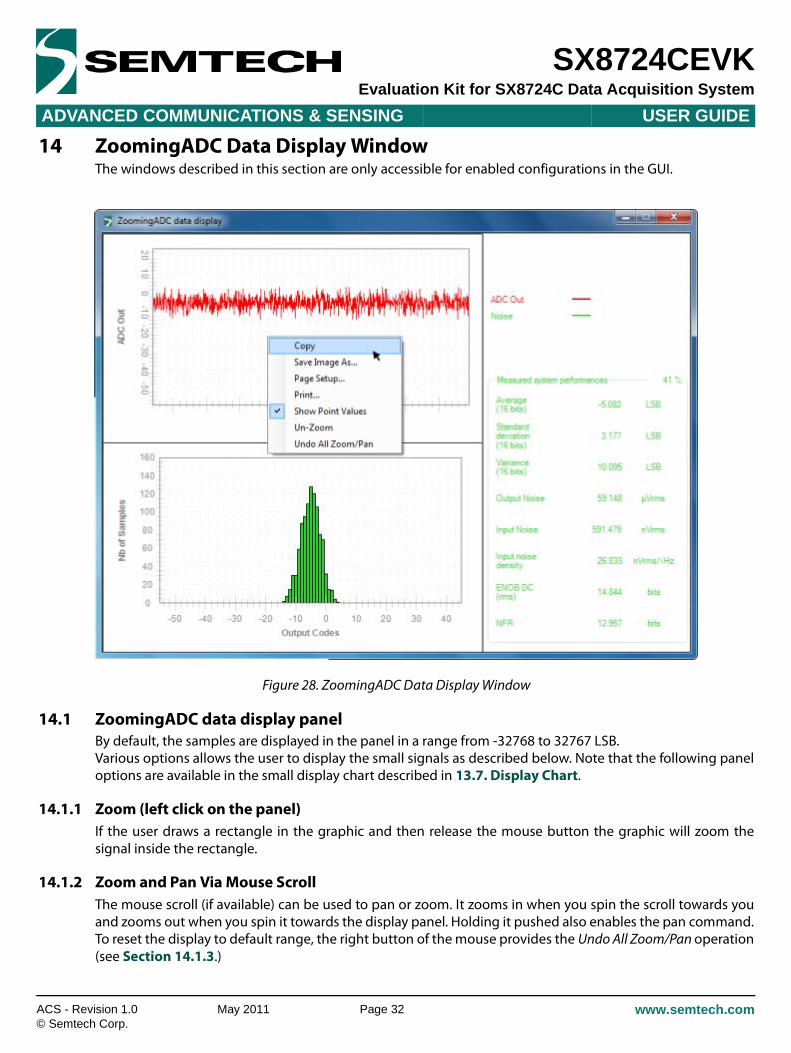
14 ZoomingADC Data Display WindowThe windows described in this section are only accessible for enabled configurations in the GUI.
14.1 ZoomingADC data display panelBy default, the samples are displayed in the panel in a range from -32768 to 32767 LSB.Various options allows the user to display the small signals as described below. Note that the following paneloptions are available in the small display chart described in 13.7. Display Chart.
14.1.1 Zoom (left click on the panel)If the user draws a rectangle in the graphic and then release the mouse button the graphic will zoom thesignal inside the rectangle.
14.1.2 Zoom and Pan Via Mouse ScrollThe mouse scroll (if available) can be used to pan or zoom. It zooms in when you spin the scroll towards youand zooms out when you spin it towards the display panel. Holding it pushed also enables the pan command.To reset the display to default range, the right button of the mouse provides the Undo All Zoom/Pan operation(see Section 14.1.3.)
Figure 28. ZoomingADC Data Display Window

www.semtech.comPage 33
ADVANCED COMMUNICATIONS & SENSING USER GUIDE
SX8724CEVKEvaluation Kit for SX8724C Data Acquisition System
ACS - Revision 1.0 May 2011© Semtech Corp.
14.1.3 Display Options (right click on the panel) Copy... allows the user to copy the display panel into the clip-board. Then the curve can be past in any other program.
Save Image As... allows to save the display panel into various common picture formats.
Page Setup... provides the settings for printing the panel
Print... allows to select an installed printer and print the display panel.
Show points Values displays the sample value by pointing on any location on the curve.
Un-Zoom allows the user to zoom out (with a small step) the display panel if the wheel is not available.
Undo All Zoom/Pan resets the display range to it’s default values.
14.2 Histogram Panel - Noise AnalysisThe distribution of the codes from the acquired signal can be seen on the Histogram panel.The Histogram graph is computed from a buffer of 1000 consecutive samples. Therefore, the refresh rate isdependant of the sample rate. If the signal is DC, the distribution width shows the noise.The samples are coded on 16 bits, if the digital resolution is set to lower than 16bits, some output codes willnever be hit.
14.3 Measured System PerformancesThe right value for the Measured System Performances is correct only when the DC signal is applied on theinputs. The values expressed in Volt units [V] are function of the VREF voltage set by the user (13.5. VoltageControl) in the GUI.
The measured system performances are computed as follows:
Average– average of the code distribution measured on a buffer of 1000 samples. If the input is 0V, the average is equal to the output offset:
Standard Deviation – the standard deviation is the rms value (Root Mean Square) of the code distribution:
Output noise – the output noise rms VN,OUT is computed with the standard deviation of the code distribution:
Input referred noise – VN,IN is the rms noise referred to the input. This parameter is computed from the output rms noise (code) and the total PGA gain:
μ 1N----Σ samples( )= LSB[ ]
σ 1N----Σ sample average–( )2
= LSB[ ]
VN OUT, σVREF
216
------------×= Vrms[ ]
VN IN,VN OUT,GDtot------------------= Vrms[ ]

www.semtech.comPage 34
ADVANCED COMMUNICATIONS & SENSING USER GUIDE
SX8724CEVKEvaluation Kit for SX8724C Data Acquisition System
ACS - Revision 1.0 May 2011© Semtech Corp.
Noise Density (referred to the input) – the input noise density VND,IN is computed according to sample rate previousely computed in the software with OSR, NELCONV and fs parameters:
ENOB DC – Effective Number Of Bits (or Effective Bits) 1– is computed according to the samples rms noise value. This value is a DC ENOB measure, not the dynamic ENOB that is measured using FFT and SINAD. Its equation is as follows:
NFR – the Noise Free Code Resolution (or flicker-free resolution) is the number of bits of resolution beyond which it is impossible to distinctly resolve individual codes. Multiplying by a factor of 6.6 converts the samples rms noise into a useful measure of peak-to-peak noise:
1.Digital averaging increases resolution and reduces noise. The effects of input-referred noise is reduced by digital averaging on the buffer of samples used to compute the Measured System Performances. Therefore, the ENOB DC value can be higher than the sample width limitation (>16 bits).
VND IN,VN IN,
samplerate----------------------------------=
Vrms
Hz-------------
σ
ENOB 16 Log2 σ( )–= bits[ ]
NFR 16 Log2 σ 6.6⋅( )–= bits[ ]

www.semtech.comPage 35
ADVANCED COMMUNICATIONS & SENSING USER GUIDE
SX8724CEVKEvaluation Kit for SX8724C Data Acquisition System
ACS - Revision 1.0 May 2011© Semtech Corp.
15 Registers Display WindowAs outlined in Section 13.2. Window Tool Bar the SX8724x GUI has a show registers utility that, whenenabled from either the Menu or Windows tool bar, provides details of the status of all configuration registersthat are documented in the SX8724C datasheet.
Whenever the contents of a register are changed in the main GUI window, the corresponding registerdisplays the new contents of the register(s), highlighting changed contents in red for a period ofapproximately 5 seconds before reverting back to black.
The register window is displayed below in Figure 29.
16 Verification Mode WindowWhen no board is connected to the PC, launching the application results in the GUI display being grayed outand the user is unable to enter data.
By depressing the <CTRL>+<ALT>+<N> keys of the PC keyboard simultaneously, the user can write to theconfiguration registers to verify propose settings, as well as load and save configuration files (*.cfg).
Figure 29. SX8724x Registers Display Window

www.semtech.comPage 36
ADVANCED COMMUNICATIONS & SENSING USER GUIDE
SX8724CEVKEvaluation Kit for SX8724C Data Acquisition System
ACS - Revision 1.0 May 2011© Semtech Corp.
APPLICATION EXAMPLES
17 Interfacing your first pressure sensor17.1 Introduction
This chapter intends to show how to interface a pressure sensor using the SX8724CEVK evaluation board.It also shows how to use efficiently the ZoomingADC™ of the SX8724C and demonstrate the benefits of thezooming feature.
17.2 Pressure SensorThe chosen sensor for this application is a 200kPa absolute pressure sensor type MPX2202AP by Freescale.Its main characteristics are described in the table below:
Table 3. Sensor main characteristics
Characteristic Value (Typ) Unit
Pressure range 0-200 kPa
Supply voltage 3.3 Vdc
Supply current 3.3 mAdc
Full scale span 3.3 mVdc

www.semtech.comPage 37
ADVANCED COMMUNICATIONS & SENSING USER GUIDE
SX8724CEVKEvaluation Kit for SX8724C Data Acquisition System
ACS - Revision 1.0 May 2011© Semtech Corp.
17.2.1 Sensor Pinout & Schematic
17.2.2 Sensor Transfer FunctionThe transfer function of the sensor is given in the figure below. It shows the output voltage (min., typ. andmax.) as a function of the absolute input pressure for the specified supply voltage.
Note: The given transfer function in the datasheet is for a 10V power supply, here the transfer function wastranslated for a 3.3V power supply.
Figure 30. Pressure sensor pin out & equivalent schematic
Figure 31. Sensor transfer function
PIN 1
1234
VS
SensingElement
Vout+
Vout-
2
3
4
1GND
Sensor output Voltage vs Pressure @ 3.3V supply
-2
0
2
4
6
8
10
12
14
16
0 20 40 60 80 100 120 140 160 180 200
Pressure [kPa]
Out
put V
olta
ge [m
VDC
]
MinTypMax
www.semtech.comPage 38
ADVANCED COMMUNICATIONS & SENSING USER GUIDE
SX8724CEVKEvaluation Kit for SX8724C Data Acquisition System
ACS - Revision 1.0 May 2011© Semtech Corp.
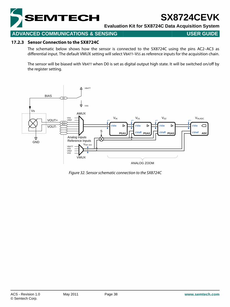
17.2.3 Sensor Connection to the SX8724CThe schematic below shows how the sensor is connected to the SX8724C using the pins AC2–AC3 asdifferential input. The default VMUX setting will select VBATT–VSS as reference inputs for the acquisition chain.
The sensor will be biased with VBATT when D0 is set as digital output high state. It will be switched on/off bythe register setting.
Figure 32. Sensor schematic connection to the SX8724C
PGA1 PGA2 PGA3 ADC
±Vin ±Vin ±Vin±Vin
±Voff ±Voff ±Vref
AMUX
Analog Inputs
VMUX
Reference Inputs
VIN VD1 VD2 VIN,ADC
VREF,ADC
VSSVREF
VSSVBATT
VSSVREF
ANALOG ZOOM
S
GND
BIAS
VOUT+
VOUT-
Vs
D0
AC3AC2
VBATT
VSS
www.semtech.comPage 39
ADVANCED COMMUNICATIONS & SENSING USER GUIDE
SX8724CEVKEvaluation Kit for SX8724C Data Acquisition System
ACS - Revision 1.0 May 2011© Semtech Corp.
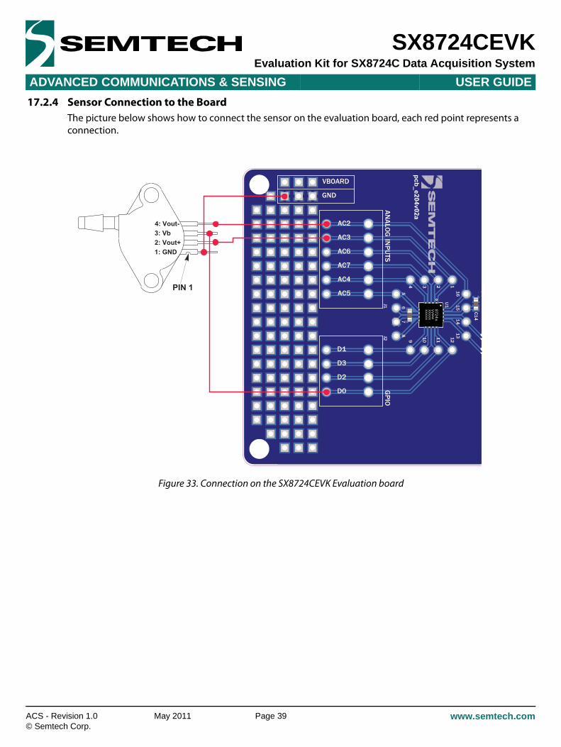
17.2.4 Sensor Connection to the BoardThe picture below shows how to connect the sensor on the evaluation board, each red point represents aconnection.
Figure 33. Connection on the SX8724CEVK Evaluation board
PIN 1
1: GND2: Vout+3: Vb4: Vout-
4
pcb_e204v02a

www.semtech.comPage 40
ADVANCED COMMUNICATIONS & SENSING USER GUIDE
SX8724CEVKEvaluation Kit for SX8724C Data Acquisition System
ACS - Revision 1.0 May 2011© Semtech Corp.
17.3 Using the Evaluation Board and the GUI
17.3.1 Configuration1. Connect the sensor to the board as described in Figure 33 on page 39.2. Select the power supply of the evaluation board to 3.3V (see chapter “Power Supply Selection” on
page 13 of the evaluation board user’s guide).3. Connect the USB connector to the evaluation board and to the PC to power the board.4. Launch the Graphical User Interface.5. Start the connection to the EVK in the GUI.
17.3.2 Voltages SettingsIn the “Voltages” group of controls, set the VBATT value to the corresponding value selected on the board:3.3V. This has no influence for the board itself but allows correct data calculation in the GUI.
17.3.3 Sensor BiasingAfter a Power-on-reset the GPIO are set to a digital output low state. The sensor bias is connected to D0 pin.Switch ON the “D0” “Out” control to set this GPIO as output high state to drive the sensor.
Figure 34. “Voltages” settings in the GUI
Figure 35. “GPIO” settings

www.semtech.comPage 41
ADVANCED COMMUNICATIONS & SENSING USER GUIDE
SX8724CEVKEvaluation Kit for SX8724C Data Acquisition System
ACS - Revision 1.0 May 2011© Semtech Corp.
17.4 Reading the sensor using the GUIBy default, if no configuration file is loaded the SX8724C state should look like in the picture beside.Press the“Set Default” button to start a default continuous acquisition mode to enable the acquisition chain.
17.5 Reference Voltage SelectionAfter having pressed the “Set Default” button as described in "17.4 Reading the sensor using the GUI", theGUI sets the input reference (VMUX) to VREF (VREF-VSS). Change this and select VBATT as voltage reference forthe acquisition chain. The “Reference” configuration control should look like the picture below
Figure 36. SX8724C default state
Figure 37. Reference Voltage Selection
Press the Set Default button here

www.semtech.comPage 42
ADVANCED COMMUNICATIONS & SENSING USER GUIDE
SX8724CEVKEvaluation Kit for SX8724C Data Acquisition System
ACS - Revision 1.0 May 2011© Semtech Corp.
17.5.1 Inputs ConfigurationSelect the AC3-AC2 analog inputs in differential mode as input chanel. The “Inputs” configuration controlsshould look like the picture below
Note: Function of the layout and the used sensor, to avoid crossing sensor Vout+ and Vout- on a board theSX8724C allows inverting the polarity of the inputs we will use the “sign inversion” feature during SX8724Cconfiguration.
17.5.2 Rough Gain ConfigurationAs the transfer function shows, the total span of the sensor is 14.5mV and the total span of the ZoomingADCis 3.3V (VBATT).The gain that needs to be applied to see the full range of the signal is then calculated as follows:
This means PGA1 gain GD1=10, PGA2 gain GD2=10 and PGA3 gain GD3=2.25 (granularity of PGA3 = 1/12).
Figure 38. SX8724C “Reference” and “Inputs” Groups of Controls
Equation 1
2275.14
3300 ===mV
mV
SensorOut
ADCOutGain
Max
Max

www.semtech.comPage 43
ADVANCED COMMUNICATIONS & SENSING USER GUIDE
SX8724CEVKEvaluation Kit for SX8724C Data Acquisition System
ACS - Revision 1.0 May 2011© Semtech Corp.
The “PGA” controls should then look like the picture below.
17.6 ZoomingADC™ Configuration
17.6.1 Zooming on the SignalAs the sensor is supposed to work at the atmospheric pressure (max: 107.8kPa - min: 88.7kPa) we will zoomon around these values and thus use the maximum amplification as possible to get the full signal at the ADCinput.As for zoom in pictures we set a particular zone of interest called measuring window (in red below).
17.6.2 Gain ComputingTo compute the total gain that must be applied to the sensor output signal we must know 2 parameters:
1. The maximum output span of the ADC, here 3.3V2. The maximum output span value of the sensor in the measuring window, here around 8.5-4.5 = 4mV
Figure 39. SX8724C“PGA” Group of Controls Configuration
Figure 40. Zooming on the Signal
ADC input sensor voltage vs pressure
0
200
400
600
800
1000
1200
1400
1600
1800
Pressure [kPa]
Volta
ge[m
VD
C]
MinTypMax
-2
0
2
4
6
8
10
12
14
16
Pressure [kPa]
Out
put V
olta
ge [m
VDC
]
MinTypMax
Sensor output Voltage vs Pressure @ 3.3V supply
89 91 93 95 97 99 101 103 105 1070 20 40 60 80 100 120 140 160 180 200
Measuring windowMeasuring window

www.semtech.comPage 44
ADVANCED COMMUNICATIONS & SENSING USER GUIDE
SX8724CEVKEvaluation Kit for SX8724C Data Acquisition System
ACS - Revision 1.0 May 2011© Semtech Corp.
Now we can apply the following formula to get the gain:
As the total gain is more than 100, all PGAs have to be enabled to obtain a total amplification of 825. Thegains must be set as follow:
• PGA1 = 10• PGA2 = 10• PGA3 = 8.25
17.6.3 Offset CancellationThe offset computation uses the middle sensor output value at the ZoomingADC™ input as shown in theformula below:
Note: Mw stands for measuring window.
Offset removing PGA after PGAs: PGA1: Amplified sensor output = 6.5mV x 10 = 65mV PGA2: Amplified sensor output = 65mV x 10 = 650mV
Offset cancellation: min +/- 0.2 x VREF (3.3V x 0.2 = 660mV).-> The minimum value is too big we cannot use the offset cancellation of PGA2.
PGA3: Amplified sensor output = 650mV x 8.25 = 5362mV
Offset cancellation: min +/- 1/12 x VREF (1/12 x 3.3V = 275mV)-> The minimum value fits up to 19 times in 5362mV 19/12 x 3.3 = 5225mV.
Note: 19/12 = 1.583
17.6.4 Final Gains ConfigurationAs computed, the PGA gains can be raised to 825.
The offset is 19/12 (see “Offset Cancellation” on page 44), as the input signal and the reference are non-inverted, the offset has to be positive.
Equation 2
Equation 3
8254
3300 ===mV
mV
SensorOut
ADCOutGain
Max
Max
mVmVmVMwMw
Offset MinMax 5.62
5.45.8
2=−=
−=

www.semtech.comPage 45
ADVANCED COMMUNICATIONS & SENSING USER GUIDE
SX8724CEVKEvaluation Kit for SX8724C Data Acquisition System
ACS - Revision 1.0 May 2011© Semtech Corp.
The “PGA” group of controls should then look like as picture beside.
Figure 41. SX8724C “PGA” final configuration
www.semtech.comPage 46
ADVANCED COMMUNICATIONS & SENSING USER GUIDE
SX8724CEVKEvaluation Kit for SX8724C Data Acquisition System
ACS - Revision 1.0 May 2011© Semtech Corp.
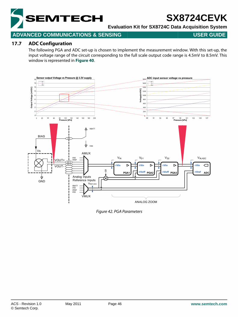
17.7 ADC ConfigurationThe following PGA and ADC set-up is chosen to implement the measurement window. With this set-up, theinput voltage range of the circuit corresponding to the full scale output code range is 4.5mV to 8.5mV. Thiswindow is represented in Figure 40.
Figure 42. PGA Parameters
ADC input sensor voltage vs pressure
0
200
400
600
800
1000
1200
1400
1600
1800
Pressure [kPa]
Volta
ge[m
VD
C]
MinTypMax
-2
0
2
4
6
8
10
12
14
16
Pressure [kPa]
Out
put V
olta
ge [m
VDC
]
MinTypMax
Sensor output Voltage vs Pressure @ 3.3V supply
PGA1 PGA2 PGA3 ADC
±Vin ±Vin ±Vin±Vin
±Voff ±Voff ±Vref
AMUX
Analog Inputs
VMUX
Reference Inputs
VIN VD1 VD2 VIN,ADC
VREF,ADC
VSSVREF
VSSVBATT
VSSVREF
ANALOG ZOOM
S
GND
BIAS
VOUT+
VOUT-
Vs
D0
AC 3AC 2
VBATT
VSS
89 91 93 95 97 99 101 103 105 1070 20 40 60 80 100 120 140 160 180 200

www.semtech.comPage 47
ADVANCED COMMUNICATIONS & SENSING USER GUIDE
SX8724CEVKEvaluation Kit for SX8724C Data Acquisition System
ACS - Revision 1.0 May 2011© Semtech Corp.
Table 4. ADC Configuration
Characteristic Value (Typ) Unit
VBATT = VREF 3.3 V
Sampling frequency 250 kHz
Gain of PGA1 10 V/V
Gain of PGA2 10 V/V
Gain of PGA3 8.25 V/V
Total PGA gain 825 V/V
Offset of PGA2 0.00 VREF
Offset of PGA3 1.58 VREF
Total equivalent input offset 6.33 mV
Over-sampling rate 512
Elementary conversions 2
Resolution1
1. ADC quantization noise only
16 bit
Conversion time 4.108 ms
LSB equivalent input voltage 62.47 nV
Equivalent input noise2
2. PGA white noise included
649E-09 Vrms
PGA settling time 2.048 ms

www.semtech.comPage 48
ADVANCED COMMUNICATIONS & SENSING USER GUIDE
SX8724CEVKEvaluation Kit for SX8724C Data Acquisition System
ACS - Revision 1.0 May 2011© Semtech Corp.
17.8 Noise CancellationThe OSR and NELCONV parameters can be increased in order to reduce the noise generated by the ADC andPGAs.
Noise with OSR=512, NELCONV=2:
Noise with OSR=1024, NELCONV=8:

www.semtech.comPage 49
ADVANCED COMMUNICATIONS & SENSING USER GUIDE
SX8724CEVKEvaluation Kit for SX8724C Data Acquisition System
ACS - Revision 1.0 May 2011© Semtech Corp.
17.9 LSB EquivalenceUsing the defined ADC and PGA set-up, an equivalent input pressure per LSB can be calculated. Using thetypical sensor transfer function, we obtain:
The approximate equivalence between Pressure and altitude is defined as follow:
This implementation has a resolution of 8cm altitude.
Equation 4
Equation 5
PressureVLSB pressureRange⋅sensorVoltageRange-------------------------------------------------------- 63nV 200kPa⋅
13.04mV------------------------------------- 0.96Pa= = =
Altitude 100kPa 8620m≡ 0.96Pa 8620m⋅100kPa
---------------------------------------→ 0.0079Pa= =

www.semtech.comPage 50
ADVANCED COMMUNICATIONS & SENSING USER GUIDE
SX8724CEVKEvaluation Kit for SX8724C Data Acquisition System
ACS - Revision 1.0 May 2011© Semtech Corp.
17.10 ZoomingADC™ BenefitsNow that we zoomed on the signal, we can compare the zoom performances with and without the offsetcompensation. To make a comparison do as follow:
Without Zoom (gain only)
1. On the graph, set the full scale view: right click on the panel and select Undo All Zoom/Pan option to reset the display range to the default full scale range.
2. Set the configuration to Gain = 225 & no offset cancellation as in 17.5.2. Rough Gain Configuration section.
3. Then blow in the sensor tube (try to make the maximum signal span).The signal span correspond to 31923–28599 = 3324 bits. The result should look like the picture below:
With Zoom (gain and offset)Now set the parameters as defined in 17.6.4. Final Gains Configuration (Gain 825, offset -1.58 x VREF). Theresult should look like the picture below:
The signal span is 11743–1374=10370 bits which corresponds to a 320% gain on the signal readingallowing you to have more consistent readings.
Figure 43. Signal Span Using Rough Gain Setting
Figure 44. Signal Span Using Zooming Settings
3324 bits span
10’370 bits span

ACS - Revision 1.0 May 2011© Semtech Corp.
www.semtech.comPage 51
ISO9001CERTIFIED
Semtech Corporation Advanced Communications & Sensing Products
Contact information
E-mail: [email protected] or [email protected]: http://www.semtech.com
USA 200 Flynn Road, Camarillo, CA 93012-8790.Tel: +1 805 498 2111 Fax: +1 805 498 3804
FAR EAST 12F, No. 89 Sec. 5, Nanking E. Road, Taipei, 105, TWN, R.O.C.Tel: +886 2 2748 3380 Fax: +886 2 2748 3390
EUROPE Semtech Ltd., Units 2 & 3, Park Court, Premier Way, Abbey Park Industrial Estate, Romsey, Hampshire, SO51 9DN.Tel: +44 (0)1794 527 600 Fax: +44 (0)1794 527 601
© Semtech 2011All rights reserved. Reproduction in whole or in part is prohibited without the prior written consent of the copyrightowner. The information presented in this document does not form part of any quotation or contract, is believed to beaccurate and reliable and may be changed without notice. No liability will be accepted by the publisher for anyconsequence of its use. Publication thereof does not convey nor imply any license under patent or other industrial orintellectual property rights. Semtech assumes no responsibility or liability whatsoever for any failure or unexpectedoperation resulting from misuse, neglect improper installation, repair or improper handling or unusual physical orelectrical stress including, but not limited to, exposure to parameters beyond the specified maximum ratings oroperation outside the specified range.
SEMTECH PRODUCTS ARE NOT DESIGNED, INTENDED, AUTHORIZED OR WARRANTED TO BE SUITABLE FOR USE IN LIFE-SUPPORT APPLICATIONS, DEVICES OR SYSTEMS OR OTHER CRITICAL APPLICATIONS. INCLUSION OF SEMTECHPRODUCTS IN SUCH APPLICATIONS IS UNDERSTOOD TO BE UNDERTAKEN SOLELY AT THE CUSTOMER’S OWN RISK.Should a customer purchase or use Semtech products for any such unauthorized application, the customer shallindemnify and hold Semtech and its officers, employees, subsidiaries, affiliates, and distributors harmless against allclaims, costs damages and attorney fees which could arise.
Notice: All referenced brands, product names, service names and trademarks are the property of their respectiveowners.
ADVANCED COMMUNICATIONS & SENSING USER GUIDE
SX8724CEVKEvaluation Kit for SX8724C Data Acquisition System

Mouser Electronics
Authorized Distributor
Click to View Pricing, Inventory, Delivery & Lifecycle Information: Semtech:
SX8724CEVK