Embed Size (px)
Citation preview

www.advmat.dewww.MaterialsViews.com
REV
IEW
Gustaaf Van Tendeloo , * Sara Bals , Sandra Van Aert , Jo Verbeeck , and Dirk Van DyckAdvanced Electron Microscopy for Advanced Materials
The idea of this Review is to introduce newly developed possibilities of advanced electron microscopy to the materials science community. Over the last decade, electron microscopy has evolved into a full analytical tool, able to provide atomic scale information on the position, nature, and even the valency atoms. This information is classically obtained in two dimensions (2D), but can now also be obtained in 3D. We show examples of applications in the fi eld of nanoparticles and interfaces.
1. The Electron Microscope: Recent History and Present Status
Understanding the world around us has intrigued humankind since time immemorial. With time we have developed tools and instruments to look deeper and deeper into nature and its struc-ture. Materials scientists try to understand and predict the prop-erties of natural materials, and to develop new materials, not formed in nature, with innovative properties. Among the latter category are, for example, the high T c superconductors, nano-materials and layered materials with multiferroic properties.
Microscopy, and in particular optical microscopy has always been a technique to improve the (poor) human eyesight. For example, in classical metallurgy or fracture mechanics optical microscopy is still very much used. At the end of the 19 th cen-tury, Ernst Karl Abbe stated that the resolution of the optical microscope is limited by the wavelength of light, i.e., of the order of half a micrometer. [ 1, 2 ] After Paul Dirac demonstrated the duality of particle and wave, Hans Busch showed that a magnetic fi eld could deviate or focus an electron beam. Next, Ernst Ruska and Max Knoll took up the challenge to construct a microscope based on accelerated electrons. [ 3 ] The primary idea was to beat the resolution of the optical microscope. In 1931, they presented their fi rst results using a “home built” instru-ment. The magnifi cation of their instrument was only 17 times at that time, but less than two years later Ruska achieved a resolution of 50 nm. Unfortunately, virtually all materials were burnt to a cinder under the electron beam and the initial interest of scientists faded away.
After World War II, technology of the electron microscope improved very fast and improving the resolution was one of the key objectives. Different European, American and Japanese
© 2012 WILEY-VCH Verlag GmbH & Co. KGaA, Weinheim
Prof. G. Van Tendeloo, Prof. S. Bals, Prof. S. Van Aert, Prof. J. Verbeeck, Prof. D. Van DyckElectron Microscopy for Materials Research (EMAT)University of AntwerpGroenenborgerlaan 171, B-2020 Antwerp, Belgium E-mail: [email protected]
DOI: 10.1002/adma.201202107
Adv. Mater. 2012, 24, 5655–5675
companies were involved in this race. In the middle of the 1950s, Menter [ 4 ] impressed the scientifi c community by showing lattice resolution and lattice imperfections with a resolution of approxi-mately 1 nm. The fi rst atomic resolu-tion images of heavy atoms such as for example thorium or gold appeared in the beginning of the 1970s. [ 5–8 ] This triggered a whole new area of research on defect studies at an atomic or nearly atomic scale.
Iijima was one of the pioneers in the fi eld of solid-state chem-istry and impressed the world with his high resolution studies of Nb 2 O 5 based materials. [ 9,10 ] During the 1980s and the 1990s, the resolution steadily improved and by the turn of the century the instrumental resolution of most commercial instruments was found to be in the range of 0.1–0.2 nm. At that time, the limit seemed to be reached since especially spherical aberration and chromatic aberration limited further progress.
The introduction of spherical aberration-corrected lenses [ 11 ] opened a new level of subangstrom resolution and improved signal-to-noise ratio. A state of the art description is given by Urban. [ 12 ] For the materials scientist, the introduction of Cs (and Cc) corrected microscopes has drastically infl uenced and improved the applications of modern electron microscopy. This includes the possibility to obtain structural information down to the atomic scale even at low acceleration voltages. In the 1960s and 1970s, researchers, as well as commercial com-panies, pushed up the accelerating voltage of microscopes, in order to benefi t from the decreased wavelength of the electrons for voltages of 1 MeV or higher. This increased voltage had the extra effect that the penetration depth increased and that much thicker samples could be analysed. Nowadays, with the increased interest in nanostructured materials, nanotubes and single sheet materials such as graphene, the tendency is more towards lower voltages. Aberration-corrected (scanning) trans-mission electron microscopy ((S)TEM) at voltages of 40 keV and even lower can be carried out with subangstrom resolution. This is of great importance for beam-sensitive materials as will be discussed further in this paper.
It must be stressed that now we can have spatial resolution at the atomic scale not only in transmission electron microscopy (TEM) mode or in scanning transmission electron microscopy (STEM) mode, but also in electron energy loss spectroscopy (EELS) mode or in energy dispersive X-ray spectroscopy (EDX) mode yielding chemical and eventually electronic information at that same level. However, the major challenge is to correctly interpret the underlying data. This reminds us of the words we heard from our group founder Severin Amelinckx more than three decades ago: “you can believe what you see … as long as you understand how you see.” These words are even more valid
5655wileyonlinelibrary.com

5656
www.advmat.dewww.MaterialsViews.com
REV
IEW Gustaaf Van Tendeloo studied
physics and graduated from the University of Antwerp in 1974. He is a professor at the University of Antwerp and part-time professor at the University of Brussels. His research focuses on the application of electron microscopy to different aspects of materials science. He is the head of the electron
microscopy group EMAT and director of the Nano Center of Excellence of the University. In 2009, he received an ERC Advanced Grant.
Sara Bals received her Ph.D. from the University of Antwerp in 2003. Next, she joined the National Center for Electron Microscopy at the Lawrence Berkeley National Laboratory (Berkeley, California). Afterwards, she returned to EMAT where she is now a senior lecturer. Her main research interest con-sists of the application and
further development of electron tomography for advanced nanostructured materials. She is also interested in the application of novel electron microscopy techniques to soft materials.
Sandra Van Aert received her Ph.D. at the Delft University of Technology (The Netherlands) in 2003. Thereafter, she joined the Electron Microscopy for Materials Research (EMAT) group of the University of Antwerp (Belgium) where she became a senior lecturer in 2009. Her research focuses on new developments in the
fi eld of model-based electron microscopy aiming at quan-titative measurements of atomic positions, atomic types, and chemical concentrations with the highest possible precision.
now that a new dimension has been added to electron micro-scopy and (artifi cially) colored images have become standard. Therefore, quantitative analysis of the experimental data is vital for a correct representation of the results. This implies (among other things) that all measurements should be accompanied by their error bars.
The impact of electron microscopy in the development of materials science and materials technology cannot be over-estimated. All applications tend towards miniaturization and approach the dimensions of the ultimate building block – the atom! Defects, interfaces and surfaces make that the atoms are deviating from their equilibrium bulk positions and give rise to strain. In all of these examples, a quantitative analysis down to an atomic scale is extremely important. Furthermore, nano-science is gradually evolving from describing to understanding to designing , where the interplay between theory and experiment will lead to the fabrication of nanostructures with designed properties. This interplay however needs a quantitative commu-nication language. Fortunately, nature itself provides the ideal language since matter consists of discrete atoms and all the structure-property relationships are unambiguously coded in the positions of these atoms. Hereby, the important questions to be answered are: where are the atoms, which atom is it, and what is its electronic confi guration? High resolution (S)TEM can (eventually) provide answers on the following aspects: what is the precision on the position of the atoms and how much are they shifted with respect to their equilibrium position. EELS or EDX can nowadays provide chemical information down to the atom column resolution and recently it has been shown that the ionic valence can also be determined, atom column by atom column.
Finally, all of these techniques can be expanded to three dimensions, mostly at nanometer level. The ultimate goal is to achieve 3D electron tomography with atomic resolu-tion. Although this is not yet possible for all structures, sig-nifi cant progress has recently been achieved using different approaches. [ 13–15 ] All of these developments are of enormous help towards the synthesis of new (nano)materials and to nano-technology in general. [ 16 ]
2. Electron Microscopy Challenges
2.1. Structural Imaging
During the last decades, the fi eld of TEM has been character-ized by technological breakthrough in microscopy design. These developments aim at an improvement of the resolution in order to simplify the direct visual interpretation of the images. Nowadays, a resolution of the order of 50 pm can be achieved by state-of-the-art instrumentation. [ 17 ] With the development of aberration correctors, [ 18 ] the resolution of a TEM image is no longer limited by the quality of the lenses but is restricted by the “width” of the atom itself which is determined by the electrostatic potential and the thermal motion of the atom. [ 19 ] Whenever that limit is reached, the images contain all the infor-mation that can be obtained using electrons. The information content is similar for experiments performed in Fourier space
wileyonlinelibrary.com © 2012 WILEY-VCH Verlag G
(diffraction) or in real space (imaging), since the waves in both spaces are mutually linked by a Fourier transform. The advan-tage of imaging as compared to diffraction is that the experi-mental data are obtained in the same space as the structure, greatly facilitating the interpretation of the images in terms of the structural parameters. Nevertheless, as discussed above, in
mbH & Co. KGaA, Weinheim Adv. Mater. 2012, 24, 5655–5675

www.advmat.dewww.MaterialsViews.com
REV
IEW
order to properly extract all information encoded in an atomic resolution image, quantitative methods are required.
The ultimate goal when applying quantifi cation techniques in the fi eld of TEM is to retrieve numerical values for unknown structure parameters with high precision. These parameters can be, for example, atom positions, atom types, chemical concen-trations, or number of atoms in a column. The precision with which atom positions have to be measured should be of the order of 1 pm. [ 20 ] As already mentioned in Section 1, extremely small changes in the local structure of nanomaterials may result into signifi cant changes of their properties. For example, strain induced by the lattice mismatch between a substrate and the superconducting layer grown on top may double its critical temperature, T c . [ 21 ]
2.1.1. Resolution Versus Precision
The question arises how to measure atom positions with picom-eter precision if the resolution of the instrument is “only” 50 pm under optimal conditions. Resolution and precision are indeed different notions. In TEM, resolution expresses the ability to visually distinguish neighboring atomic columns in an image. Classical resolution criteria, such as Rayleigh’s, are derived from the assumption that the human visual system needs a minimal contrast to discriminate two points in its composite intensity distribution. [ 22 ] Therefore, they are expressed in terms of the width of the point spread function of the TEM imaging system. [ 23 ] However, if the physics behind the image formation process is known, images no longer need to be interpreted visu-ally. Instead, atomic column positions can be estimated by fi tting a model to an experimental image. [ 24,25 ] In the absence of noise, this procedure would result in an infi nitely precise reconstruc-tion of the atomic column locations. Since detected images are never noise-free, model fi tting never results in a perfect recon-struction thus limiting the statistical precision with which the atom locations can be estimated. Under certain assumptions, it can be shown that the attainable precision, expressed in terms of the standard deviation with which the position of a projected atomic column can be estimated, is proportional to the instru-mental resolution and inversely proportional to the square root of the number of detected electrons. [ 26–27 ] This explains why the precision to estimate projected atomic column positions can be down to 1 or a few picometers although the resolution of modern instruments is 50 to 100 pm. For instance, if one wants to obtain the position of an atom with a precision of the order of 1 pm, one will need an incident dose of electrons of the order of 1000 electrons per Å 2 . In order to push the precision further by a factor of 10, it is necessary to increase the dose by a factor of 100, which will require a very high brightness and/or a long exposure time.
2.1.2. Quantifi cation in TEM Mode
Aberration-corrected TEM, [ 11 , 18 , 28 ] exit wave reconstruc-tion methods [ 29–31 ] or combinations of both are often used to measure shifts of the atomic positions. Whereas aberration correction has been discussed in Section 1, the purpose of exit wave reconstruction is to retrieve the complex electron wave function which is formed at the exit plane of the sample under
© 2012 WILEY-VCH Verlag GmAdv. Mater. 2012, 24, 5655–5675
study. In practice, the exit wave is usually reconstructed from a series of images taken at different defocus values, [ 29 ] from an electron holographic image [ 30 ] or from a series of images recorded with different illuminating beam tilts. [ 31 ] Ideally, the exit wave is free from any imaging artifacts thus enhancing the visual interpretability of the atomic structure. Because of its potential to visualize light atomic columns, such as oxygen or nitrogen, [ 32,33 ] with atomic resolution, exit wave reconstruc-tion has become a powerful tool in high resolution TEM. Although such a reconstruction was often considered as a fi nal result used to visually interpret the structure, its combination with quantitative methods nowadays demonstrates its poten-tial to precisely measure atomic column positions. [ 34–36 ] As an example, the quantifi cation of localized displacements at a {110} twin boundary in orthorhombic CaTiO 3 will be discussed in Section 3.2. [ 37 ]
Another effi cient technique to measure shifts of the atomic positions is so-called negative-spherical-aberration imaging in which the spherical aberration constant, Cs, is tuned to nega-tive values by employing an aberration corrector. [ 38 ] Compared with traditional positive Cs imaging, this imaging mode yields a negative phase contrast of the atomic structure, with atomic col-umns appearing bright against a darker background. For thin objects, this leads to a substantially higher contrast compared to the dark atom images formed under positive Cs imaging. This enhanced contrast has the effect of improving the meas-urement precision of the atomic positions and explains the use of this technique to measure atomic shifts of the order of a few picometers. Recent examples show measurements of the width of ferroelectric-domain walls in PbZr 0.2 Ti 0.8 O 3 , [ 39 ] measure-ments of the coupling of elastic strain fi elds to polarization in PbZr 0.2 Ti 0.8 O 3 /SrTiO 3 epitaxial systems [ 40 ] and of oxygen-octa-hedron tilt and polarization in LaAlO 3 /SrTiO 3 interfaces. [ 41 ]
2.1.3. Quantifi cation in STEM Mode
In the imaging techniques described in Section 2.1.1 the specimen is illuminated by a near parallel beam of electrons. However, a different imaging variant to investigate local atomic arrangements is STEM in which a focused probe scans across the specimen in a two-dimensional raster. [ 8 ] For each probe position, a diffraction pattern is formed in the back focal plane, where a detector is located. Only that part of the diffrac-tion pattern reaching the detector is integrated and displayed as a function of the probe position. Depending on the shape and size of the detector, different signals can be recorded. [ 42 ] A key imaging mode is high angle annular dark fi eld (HAADF) STEM in which an annular detector is used with a collection range outside of the illumination cone. The high angle scat-tering thus detected is dominated by Rutherford and thermal diffuse scattering. Therefore, the HAADF signal approximately scales with the square of the atomic number, Z, hence the name Z-contrast. One of the advantages is thus the possibility to visu-ally distinguish between chemically different atomic column types. Because of the incoherent imaging nature, the resolu-tion observed in an HAADF STEM image is to a large extent determined by the intensity distribution of the illuminating probe. [ 43 ] The use of aberration-corrected probe forming optics currently gives a probe size of the order of 50 picometers. [ 44 ]
5657wileyonlinelibrary.combH & Co. KGaA, Weinheim

5658
www.advmat.dewww.MaterialsViews.com
REV
IEW
The combination of a high spatial resolution with a high chem-ical sensitivity makes HAADF STEM a very attractive tool for structure characterization at the atomic level.
Even though HAADF STEM images are to a certain extent directly interpretable, also this imaging technique may greatly benefi t from a quantitative analysis such as statistical param-eter estimation theory. [ 45 ] This is particularly the case when the difference in atomic number of distinct atomic column types is small or if the signal-to-noise ratio becomes poor. A perform-ance measure which is sensitive to the chemical composition is the scattering cross section. Using statistical parameter esti-mation theory, the total intensity of scattered electrons can be quantifi ed atomic column by atomic column using an empir-ical parameterized incoherent imaging model. The obtained measurements allow us to differentiate between atomic col-umns with different composition. As such, differences in aver-aged atomic number of only 3 can clearly be distinguished in an experimental image which is impossible by means of visual interpretation only. This is an important advantage when stud-ying interfaces as illustrated in the following example. Figure 1 a shows an enlarged area from an experimental HAADF STEM image of a La 0.7 Sr 0.3 MnO 3 –SrTiO 3 multilayer structure using a FEI Titan 3 50–80 operated at 300 kV. Even though the probe has been corrected for spherical aberration, no visual conclusions could be drawn concerning the sequence of the atomic planes
wileyonlinelibrary.com © 2012 WILEY-VCH Verlag Gm
Figure 1 . a) Region from an experimental HAADF STEM image of a La 0.7 Sc) Overlay indicating the estimated positions of the columns together with tof the known columns.
at the interfaces. The refi ned parameterized model is shown in Figure 1 b showing a close match with the experimental data. Figure 1 c shows the experimental observations together with an overlay indicating the estimated positions of the columns and their atomic column types. The composition of the columns away from the interfaces is assumed to be in agreement with the composition in the bulk compounds whereas the composition of the columns in the planes close to the interface (indicated by the symbol “X”) is unknown. Histograms of the estimated peak volumes of the known columns are presented in Figure 1 d and show the random nature of the result. The colored vertical bands correspond to 90% tolerance intervals. It is important to note that these tolerance intervals are not overlapping meaning that columns, for which the difference in averaged atomic number is only 3 (TiO and MnO) in this example, can clearly be distinguished. Based on this histogram, the composition of the unknown columns could be identifi ed as shown on the right-hand side of Figure 1 c. Single-colored dots are used to indicate columns whose estimated peak volume falls inside a tolerance interval whereas pie charts, indicating the presence of inter-mixing or diffusion, are used otherwise.
The high sensitivity that can be achieved using the method described above is an advantage to count the number of atoms in a column with single atom precision. To illustrate this, a recent achievement [ 13 ] of counting the number of atoms in a
bH & Co. KGaA, Weinheim
r 0.3 MnO 3 –SrTiO 3 multilayer structure. b) Refi ned parameterized model. heir atomic column types. d) Histograms of the estimated peak volumes
Adv. Mater. 2012, 24, 5655–5675

www.advmat.dewww.MaterialsViews.com
REV
IEW
Figure 2 . a) Experimental HAADF STEM image of nanosized Ag clusters embedded in an Al matrix in the [101] zone-axis orientation. b) Refi ned para-meterized model of the boxed region of (a). c) Number of Ag atoms per column. d) Histogram of scattered intensities of the Ag columns. e) Integrated Classifi cation Likelihood criterion evaluated as a function of the number of Gaussians in a mixture model. f) Experimental HAADF STEM image in [100] zone-axis orientation. g) Refi ned model of the boxed region of (f). h) Number of Ag atoms per column. i) Computed 3D reconstruction of the Ag nanocluster viewed along three different directions.
nanosized Ag cluster embedded in an Al matrix is summarized here. Figure 2 a shows an aberration-corrected HAADF STEM image of such clusters viewed along the [101] zone-axis. Using the model-based approach explained above, the parameters of an empirical physics-based empirical model have been esti-mated in the least squares sense. For the cluster in the white boxed region, the refi ned model is shown in Figure 2 b. Based on the estimated parameters, scattered intensities have been computed for each atomic column.
These are shown in the histogram in Figure 2 d. Since the thickness of the sample can be assumed to be constant over the particle area, substitution of an Al atom by an Ag atom, leads to an increase of the estimated intensity. Owing to a combina-tion of experimental detection noise and residual instabilities, broadened - rather than discrete–peaks are observed. There-fore, these results cannot be interpreted directly in terms of number of atoms in a column. However, by evaluating the so-called integrated classifi cation likelihood (ICL) criterion, as shown in Figure 2 e, the presence of 10 signifi cant peaks has been found whose positions are indicated by means of black dots in Figure 2 d. From the estimated peak positions, the number of Ag atoms in each atomic column can be quantifi ed leading to the result shown in Figure 2 c. This counting pro-cedure has also been applied to the same Ag cluster viewed along the [100] direction as shown in Figure 2 f–h. In Section 2.4.3 it will be explained how atom counting results obtained from different zone-axis orientations can be combined to retrieve the 3D atomic structure. For example, the atom
© 2012 WILEY-VCH Verlag GAdv. Mater. 2012, 24, 5655–5675
counts presented in Figure 2 c,h result in the reconstruction shown in Figure 2 i.
Since all interactions with the fast electron beam get weaker as the elements get lighter, HAADF STEM is less suitable when it comes to solve atomic structures consisting of light atoms. In HAADF STEM, the atomic number Z-dependence of the con-trast approximately scales as Z 2 . For that reason, this imaging mode tends to render columns of light elements invisible when in proximity to heavier elements. Annular bright fi eld (ABF) STEM recently re-emerged as a promising STEM mode to image light elements. [ 42 , 46 ] In this mode, an annular detector spanning a range within the illumination cone of the focused electron beam is used. The Z-dependence of ABF STEM has been very roughly estimated as Z 1/3 and is therefore better suited to observing light and heavy elements simultaneously [ 47 ] although at the expense of chemical sensitivity. Because of the importance of light elements such as lithium and hydrogen in battery and energy storage materials, ABF STEM is a very promising technique. Recent ABF STEM images of vanadium dihydride, [ 48 ] VH 2 , and of yttrium dihydride, [ 49 ] YH 2 , have dem-onstrated that it is indeed possible to image hydrogen directly. Furthermore, with the same technique, columns of Li, O, and Co ions in the lithium-ion battery cathode material LiCoO 2 have been visualized simultaneously. [ 50 ] While these examples directly observing light elements are a great step forward for the analysis of important materials, quantifying column occu-pancies and measuring the number of light atoms present will be a challenging next step.
5659wileyonlinelibrary.commbH & Co. KGaA, Weinheim

5660
www.advmat.dewww.MaterialsViews.com
REV
IEW
Figure 3 . Sketch of a STEM setup including EELS, EDX and HAADF detection. EELS and EDX spectrum of a Ca 2 FeCoO 5 sample showing typical differences in background, and excitation peaks.
2.1.4. How Low Can We Go?
A reliable way to confi rm atomic structures determined from STEM or high-resolution transmission electron microscopy (HRTEM) images is by combining them with image simulations in which the quantum mechan-ical nature of the electron-object interaction and the electron-optical imaging process are properly taken into account. In HRTEM, a quantitative comparison between the experi-mental and simulated images was for a long time hampered by the so-called contrast problem, also known as the Stobbs-factor problem. [ 51 ] The contrast in experimental images was commonly two or three times lower than in simulated images. Different physical phenomena have been consid-ered to explain this contrast problem. [ 52,53 ] Recently, it has been found that a major reason is the neglect of the detector mod-ulation-transfer function in image simula-tions. [ 54 ] Also in STEM, lower contrast in
the experimental images has been noted, [ 55 ] although here the origin of this mismatch is different than in HRTEM. [ 56 ] Here, an almost perfect agreement is found between simu-lation and experiment provided that multiple thermal dif-fuse scattering is properly modeled and spatial incoherence of the source is taken into account. [ 57,58 ] Furthermore, STEM image intensities need to be normalized with respect to the incident electron beam by taking the detector sensitivity into account. [ 57 , 59 ]Because of its optimal statistical properties, the ultimate way to determine the atomic structure in a quantitative way will be to estimate all unknown structure parameters using a com-plete maximum likelihood method. [ 24 ] Therefore, a parameter-ized joint probability density function, describing the expec-tations of the image pixel values as well as their fl uctuations around these expectations, is required. As discussed before, numerical image simulation methods now exist to accurately describe the expectation values for a given atomic structure. Such models are parametric in the quantities of interest, such as the locations of the atoms and the atom types. Furthermore, an accurate description of the detector and noise properties, taking correlations between neighboring pixel values into account, is required. [ 60,61 ] Next, the unknown structure param-eters can be estimated by maximizing the likelihood function, which can relatively easily be derived from the joint probability density function. The search for the maximum of this func-tion is an iterative numerical procedure and requires a starting structure for the parameters which is suffi ciently close to the real structure in order to avoid the risk of ending up in a local maximum. From this description, it is directly clear that this optimization procedure is far from simple and will be compu-tationally demanding. Therefore, GPU computing strategies to reduce the total computing time will be very welcome. [ 62 ] How-ever, if successful, we will be able to measure unknown struc-ture parameters as accurately and precisely as possible using a given electron dose.
wileyonlinelibrary.com © 2012 WILEY-VCH Verlag Gm
2.2. Chemical Imaging Through EELS or EDX
Modern electron microscopy reaches its ultimate poten-tial when combined with analytical techniques that provide chemical and electronic structure information. The two most commonly used techniques to obtain such chemical informa-tion are based on the inelastic scattering of fast electrons with atoms in a material. During this scattering process, an atom is excited to an unoccupied state with an energy Δ E above the ground state. The fast electron has provided this energy and loses Δ E. This loss can be determined using an EELS spec-trometer. The atom can then de-excite by emitting character-istic (X-ray) photons. These photons are consequently detected in an EDX detector and their abundance creates a near con-tinuous spectrum. Both EELS and EDX processes are physi-cally closely related but the detection of either electrons or X-rays leads to important differences in the capabilities of both techniques.
2.2.1. EELS Versus EDX
EELS profi ts from the fact that the inelastic scattering of fast electrons, with typical energy losses that are much smaller than the primary energy, is strongly forward scattered. This allows collecting the majority of the inelastically scattered electrons inside the so-called collection angle, β , as indicated in Figure 3 and leads to very high collection effi ciencies. Energy dispersion is usually obtained by making use of the Lorentz force in a region of magnetic fi eld and many different spectrometer geometries have been built, each with their own advantages and disadvantages. [ 63–69 ] A modern EELS spectrometer has a parallel recording system based on a digital camera in order to read out spectra at high speed. The spectral resolution is nowa-days fully determined by how monochromatic the electron gun can be made. In this respect, two paths are available: either the intrinsic energy spread of the electron gun is improved using
bH & Co. KGaA, Weinheim Adv. Mater. 2012, 24, 5655–5675

www.advmat.dewww.MaterialsViews.com
REV
IEW
Schottky FEGs and cold FEGs [ 70–73 ] instead of traditional LaB 6 electron guns, or using an electron monochromator. [ 74–76 ] A typical energy resolution of up to 100 meV or even lower is cur-rently possible, reaching levels of spectroscopic detail which were previously only achievable in X-ray absorption spectros-copy in synchrotron setups. [ 76 ] The remaining challenge is to decrease the energy spread without losing too much beam cur-rent in order to obtain a suffi cient signal-to-noise ratio in a rea-sonable recording time.
The X-rays used in EDX on the other hand are approximately emitted isotropically and a fi nite size detector only captures a small fraction in the solid angle Ω EDX . Solid angles approaching 1 sr have become possible recently. [ 77 ] Even with these state-of-the-art EDX detectors, only up to 8% (1/4 π ) of the total emitted X-rays are captured, making EDX a less effi cient technique as compared to EELS. Energy dispersion usually occurs in a so-called silicon drift detector with typical energy resolutions above 100 eV, about three orders of magnitude worse compared to EELS. Other techniques such as wavelength dispersive spec-troscopy (WDS) and bolometers improve the energy resolution but can not compete with EELS in terms of energy resolution and detection effi ciency. This results in the fact that EDX pro-vides only information concerning the type of atoms available in the material since detailed electronic structure information is hidden at this energy resolution. However, a major advan-tage of EDX is the fact that the characteristic peaks in EDX are usually peaked features superimposed on a low and fl at background signal caused e.g., by bremmstrahlung. This situ-ation greatly facilitates to quantify EDX spectra as compared to the complex background behavior in EELS. The favorable peak-to-background ratio also has a fundamental advantage in terms of signal-to-noise ratio since the fundamentally limiting counting noise only depends on the total signal including the background. Another drawback of the isotropic character of the X-rays is the potential for these X-rays to excite other neigh-boring atoms in a fl uorescence process. This may lead to spu-rious peaks and deteriorates the spatial resolution depending on the geometry of the sample.
Figure 3 shows a comparison between an EELS and an EDX spectrum acquired for the same sample. The difference in background between EELS and EDX is the most striking differ-ence as well as the very rich fi ne structure in the EELS excita-tion edges.
2.2.2. Quantifi cation of EELS and EDX Spectra
Similar to structural imaging, there is an increasing need for quantitative results in the fi eld of chemical imaging as well. Quantifi cation of both EDX and EELS is based on comparison with either theoretically or experimentally obtained inelastic cross sections. In EELS, the background and multiple inelastic scattering needs to be removed. Model based approaches were shown to considerably improve the precision in quantifi ca-tion leading to either higher precision or better detectability of low concentrations of elements. [ 78–83 ] Rather than using the conventional quantifi cation methods, more information can be extracted using a model based approach in a similar manner as explained in Section 2.1. Since inelastic scattering typically relies on low probability events, signal-to-noise ratios
© 2012 WILEY-VCH Verlag GmAdv. Mater. 2012, 24, 5655–5675
are usually not ideal. A straightforward approach to overcome this problem is to increase the total amount of electrons that interact with the sample by either increasing the incoming current or the exposure time. However, the gain that can be obtained, is limited since beam damage and/or sample drift will increase. A popular approach to increase the signal-to-noise ratio of a large set of existing experimental EELS data is the use of principal component analysis (PCA) and its many variants. [ 79 , 84 ] Even though the results can be striking, great care needs to be taken to avoid the introduction of artefacts and overinterpretation of the data.
Both EELS and EDX can be combined with a scanned focused electron probe to obtain analytical information with a spatial resolution that is determined approximately by the size of the probe. This method is called spectrum imaging [ 85 ] since a set of spectra is obtained from different spatial points. In this manner, atomic resolution analytical information is nowadays a commonly used technique for both EELS and EDX. [ 86–89 ] Nevertheless, the physics of the interaction is not truly local as the fast electron interacts with the sample via long range Coulomb interaction and many counterintuitive effects can make the interpretation diffi cult. In EDX, this situation is further complicated by fl uorescence and other artefacts. In order to obtain a better understanding of this complicated interaction, several groups have spent consider-able efforts to simulate the details of inelastic scattering in combination with multiple elastic scattering in many different approximations. [ 89–97 ] Although the situation is similar to the need for image simulation in HRTEM, the computational complexity of the simulation is considerably more demanding in this case. Therefore, a so-called local interpretation where the signal peaks on the atom of interest is expected for very thin samples, a large collection angle, energy losses above a few 100 eV and for isotropic bonding; however, simulations are necessary to confi rm this.
2.2.3. The Limits of Chemical Imaging
In view of the discussion above, one may wonder: how low can we go? In terms of analytical (S)TEM this is not an easy ques-tion to answer as many limits determine the performance. In terms of spatial resolution, we have seen that, atomic resolution is available although many published examples rely on a some-what large unit cell parameter in perovskites and simulations are needed to make sure that a local approximation is valid. The delocalization of inelastic scattering is in many cases larger than the probe size, which puts a physical limit on the ultimate spatial resolution that can be obtained. In terms of detectability, a clear physical limit is the fact that matter is built from indi-vidual atoms. Since it was shown that single atom detectability can be obtained in widely different situations [ 98,99 ] it seems that also here the limit is determined by the physics and not by the microscope. This situation is similar to how the ultimate res-olution of a microscope is now fundamentally limited by the atomic scattering factor and not by the instrument as discussed in Section 2.1. However, the statements described above pre-sume that the sample is stable under the required dose and channeling can be reduced, for example, by tilting away from zone axis conditions.
5661wileyonlinelibrary.combH & Co. KGaA, Weinheim

5662
www.advmat.dewww.MaterialsViews.com
REV
IEW
2.2.4. Valency Imaging Through STEM-EELSIn view of the superior energy resolution of EELS over EDX, one can exploit the additional information that is encoded in the fi ne details of the EELS excitation edges. These details are referred to as the energy loss near edge structure (ELNES) and they are related to the unoccupied density of states in a material. Indeed, if we excite a core loss excitation, only exci-tations to unoccupied states are allowed. Moreover, selection rules apply approximately, which limits the number of unoc-cupied states to those that have the required orbital angular momentum ( Δ l = ± 1, Δ m = -1,0, + 1) assuming the dipole terms are dominant. This means that we can consider ELNES as an (indirect) fi ngerprint of the electronic structure of a material. In practice, the subtle changes in ELNES can be used to detect changes in coordination symmetry, bonding and valency. Inter-preting these subtle changes in terms of, for example, the band structure is often diffi cult due to the ambiguity in the mapping of the full band structure onto a symmetry-projected unoc-cupied density of states (DOS). Nevertheless, comparing to experimental reference spectra obtained from reference mate-rials can often lead to observed trends that can be exploited in unknown materials. A good example of this is the trend that has been found in transition metal L 23 edges with respect to the valency. In a fi rst approximation, the L 23 ELNES is governed by the formal valence of the atom whereas, for example, coordina-tion effects play a less dominant role. [ 100–103 ] Empirically, one observes a shift in energy position of the peak and a change in the so-called white line ratio. If proper care is taken to correct for multiple scattering, a reliable measurement of the formal valence of a transition metal oxide can be obtained. Combining this possibility with atomic resolution STEM probes allows us to measure valence on the atomic scale. [ 104–106 ] A demonstration of this possibility is given in Figure 4 for Mn 3 O 4 .
Recently, similar experiments were able to distinguish between different coordination symmetries using subtle changes in the ELNES of the Fe and Co L 23 edges in Ca 2 CoFeO 5 . [ 107 ]
These examples demonstrate that atomic resolution is nowa-days also a reality in the fi eld of electronic structure mapping.
wileyonlinelibrary.com © 2012 WILEY-VCH Verlag
Figure 4 . Example of atomic resolution valence mapping in Mn 3 O 4 . a) HAMn ions. b) EELS spectra obtained from Mn 3 + and Mn 2 + sites showing cldistribution of the Mn 2 + and Mn 3 + signal showing their different location
This possibility holds great promise for materials science as an increasing number of devices rely on the electronic struc-ture of a single layer of atoms near, for example, an interface or a defect. The examples discussed above show how STEM EELS can be used to directly image these structures. One could imagine direct visualization of the much debated charge ordering in complex oxides, [ 108 ] or the direct visualization of the 2D electron gas at a LAO/STO interface. [ 109,110 ]
In terms of future prospects for STEM EELS, it seems that most limitations are no longer instrumental. Indeed, pos-sibly the biggest bottleneck concerning the wide application of STEM EELS is the very high dose that needs to be applied locally (e.g., typical doses are 50 pA for 10 ms per spatial posi-tion) and therefore beam damage clearly forms a (noninstru-mental) limit. In terms of energy resolution, several aspects of the instrumental setup can still be improved but for core loss ELNES this is currently not a limiting factor as so-called life-time broadening limits the resolution to 0.3 eV at best. [ 111,112 ] This means that even though the energy resolution of the instrument can nowadays reach 100 meV, more details in the fi ne structure of the core loss spectra are not to be expected. For low loss excitations the situation is fundamentally different since the lifetime of such excitations can be considerably longer and therefore improvements in monochromator instrumenta-tion are still welcome.
2.3. Magnetic Imaging
The effect of magnetic fi elds on the charged electrons in an electron microscope is fundamental to the operation of the magnetic lenses but one may wonder about the effect on the primary electrons if the sample is magnetic?
2.3.1. Magnetic Imaging Based on Elastic Scattering
In terms of elastic scattering, the fundamental effect is the quantum mechanical Aharanov Bohm (AB) effect [ 113 ] where a given electron path picks up an extra phase shift Δ φ proportional
GmbH & Co. KGaA, Weinheim
ADF STEM image with structure overlay showing the location of the different ear differences in fi ne structure related to the valency. c) Map of the spatial with atomic resolution. More details can be found elsewhere. [ 100 ]
Adv. Mater. 2012, 24, 5655–5675

www.advmat.dewww.MaterialsViews.com
REV
IEW
Figure 5 . Sketch of the different setups to measure magnetic fi elds in samples in the (S)TEM. a) Lorentz microscopy, b) Differential phase contrast, c) Off-axis electron holography. d) Experimental magnetization of a ring of Co particles obtained with electron holography. Image obtained from R.Dunin-Borkowksi similar to Ref. [ 117 ]
to the line integral of the projected magnetic vector potential along the path. This phase shift in itself is not observable, but the relative shift with respect to other paths will lead to interfer-ence effects that depend on the fl ux enclosed by the two paths probing a region around the sample. The classical Lorentz force can be seen as a macroscopic manifestation of the AB effect. The effect has been exploited in three complementary setups that are popular for studying magnetic materials: Lorentz micro-scopy in Fresnel TEM mode and in differential phase contrast STEM mode (DPC) and off-axis electron holography. [ 114 ]
The setup for Lorentz Fresnel microscopy is sketched in Figure 5 a. The fast electron wave picks up a phase shift depending on the projected magnetic vector potential along the optical axis. For a particle with a homogeneous magnetic fi eld, this would result in a phase gradient across a magnetic grain. This gradient causes a local tilting of the wave which leads to either dark or bright electron intensities at the magnetic grain boundaries for an out of focus image. These bright and dark interference bands are therefore linked to the grain boundaries and can be visualized up to a spatial resolution of 10 nm. [ 115 ] Even vortex lattices in superconducting Nb were observed in this way. [ 116 ] Calculating the observed intensities back to the exact 3D fi eld distribution is diffi cult but simulations can pro-vide some insight for relatively simple geometries. [ 115 ]
Another variant of Lorentz microscopy in STEM mode is dif-ferential phase contrast as sketched in Figure 5 b. In this case, a STEM probe is scanned over a sample and the defl ection of the probe due to the Lorentz force is measured with a four quad-rant detector or a CCD detector. [ 118–121 ] The defl ection is pro-portional to the local phase gradient caused by the AB effect but complications can arise due to diffraction effects. The fact that this method is proportional to the gradient of the phase is highly desirable over the direct measurement of the phase as the defl ection is proportional to the projection of the magnetic induction perpendicular to the beam trajectory along the beam path. [ 121 ]
A technique to observe the phase of the exit wave is off-axis electron holography [ 122–124 ] as sketched in Figure 5 c. In this approach, a charged wire is used to interfere with a reference part of the electron wave with a part that interacted with the crystal. The interference pattern now encodes the phase and amplitude information of the exit wave which can be recon-structed using Fourier transform based techniques. A diffi culty
© 2012 WILEY-VCH Verlag GmbH & Co. KGaA, WeinhAdv. Mater. 2012, 24, 5655–5675
is the fact that the phase of the electrons is not only infl uenced by the AB phase shift, but also by an electrostatic phase shift. Typi-cally, the electrostatic effect is even dominant over the magnetic contribution but can be canceled out by either reversing the external magnetic fi eld or by mechanically fl ipping over the sample. In both cases, a reversal of the magnetic phase shift is obtained while the electrostatic phase shift remains the same. Electron holography was successful in mapping the magnetization of nanoparticles and arrays of nanoparticles. [ 125 ] An example is presented in Figure 5 d. Even though holography is by far the most quantitative technique available for magnetic mapping in
the TEM, several restrictions remain. A fi rst issue is the fact that only projections of the magnetic vector potential can be obtained. This can be overcome making different projections and calculating back to obtain a 3D vector fi eld, but in practice this is far from trivial as will further be discussed in Section 2.6.4. [ 126 ] Another important issue is related to signal-to-noise. In current experiments, the phase sensitivity is estimated to be 2 π /300 [ 127,128 ] which puts a limit on the smallest amount of fl ux that can be measured. This explains why all examples in the literature are particles with sizes in the range of at least 10 nm because only for those sizes the fl ux is high enough. At present, imaging of single atoms carrying magnetic moments seems to be far out of the realm of possibilities since the expected phase shift is only of the order of 10 − 4 radians independent of the acceleration voltage.
2.3.2. New Approaches for Magnetic Imaging
In terms of elastic scattering, spin polarized electron beams might form promising candidates to obtain magnetic informa-tion. Currently, electron microscopes are being built with spin polarized beams, [ 129 ] but theoretically it is unclear how such beams would reveal magnetic information about a sample. The effect of quantum mechanical exchange between elec-trons in the sample and fast electrons in the beam is indeed a very improbable effect due to the very different kinetic energy of both electrons. Note that this is in strong contrast with low energy electron beams such as in spin polarised EELS, where exchange does play an important role and reveals magnetic information about the sample. [ 130,131 ]
Apart from the elastic effect, magnetization in samples can also be studied by using inelastic scattering. The effect hinges on dipole selection rules that state that in inelastic scattering the orbital quantum number should change by −1, 0 or + 1. [ 111 ] In the simplest case of a K-edge excitation, we have a transition from a 1s state to an unoccupied 2p state as sketched in Figure 6 . If we suppose that the magnetism on the atom is caused by orbital magnetism of the 2p electrons, than for example, the 2p −1 orbital is fi lled while the 2p + 1 may be empty. This means that for an incoming plane wave, the transition Δ m = −1 is forbidden as the fi nal state is already occupied, whereas the Δ m = + 1 transition is available. The asymmetry between Δ m = −1 and + 1 therefore carries information about the magnetization of a
5663wileyonlinelibrary.comeim

56
www.advmat.dewww.MaterialsViews.com
REV
IEW
Figure 6 . a) Sketch of a K-edge excitation of a hypothetical carbon atom with an orbital mag-netic moment of 2 μ B. The only unoccupied state that is available is the 2p + 1 state which requires an orbital angular momentum (OAM) change of the atomic electrons of Δ m a = + 1. Conservation of OAM then requires that also the primary electron changes its OAM to compen-sate ( Δ m e = −1). This change in OAM is undetectable in conventional EELS, but in the EMCD setup or making use of electron vortex beams, this change becomes detectable. b) A Co L 23 excitation edge of a Co metal sample making use of a vortex setup to detect changes in OAM of the fast electrons. Doing this makes the L 23 edge different for two symmetrical positions of the spectrometer revealing the ferromagnetic nature of the Co atoms.
specifi c atom in the sample. Unfortunately, the difference in the outgoing inelastically scattered electron wave between a Δ m = −1 and + 1 transition is only encoded in the phase of that wave and can not be detected in the probability. Two methods exist to solve this issue. The fi rst method uses the elastic scattering of the inelastic wave with the crystal to create interference effects that reveal the handedness of the outgoing wave. This method is referred to as electron energy loss magnetic chiral dichroism (EMCD), [ 132,133 ] analogous to XMCD, which uses circularly polarized X-rays. [ 134 ] The method requires a precise matching of the orientation and thickness of the sample to obtain a situation where the elastic scattering provides a π /2 phase shift and sim-ilar amplitude. This limits the method to crystalline materials with known thicknesses and requires a very precise orientation in 2 or 3 beam conditions. [ 135 ] The method was shown to reveal spectra very similar to the popular method of XMCD applied in synchrotrons but now with up to 2 nm spatial resolution. [ 136 ] Because inelastic scattering to core states has a low probability and this method hinges on small interference effects on top of this signal, a major concern is the signal-to-noise ratio that can be obtained. [ 137 ] The dependence on the Bragg scattering of the inelastic wave also implies that the technique is inher-ently limited to probe regions which are bigger than a unit cell. Atomic resolution EMCD is therefore impossible in the con-ventional setup. Alternatives have been proposed based on the asymmetric positioning of the spectrometer with respect to the optical axis in combination with focused STEM probes. In this setup, small positional shifts are obtained due to interference effects which are opposite depending on the magnetization of the atom while atomic resolution is maintained. [ 138 ]
Recently, an alternative to EMCD was demonstrated which no longer relies on the elastic scattering of the crystal to reveal magnetic information about the sample. In this method, a so-called vortex electron beam is used which contains a spiraling phase much like the outgoing inelastic electron wave after
64 wileyonlinelibrary.com © 2012 WILEY-VCH Verlag GmbH & Co. KGaA, Weinh
scattering to a magnetic material. This beam breaks the symmetry between the Δ m = + 1 and − 1 transition after which conventional intensity detection will reveal the magnetiza-tion of the sample. This vortex based EMCD comes also much closer to XMCD as the orbital angular momentum carried by the vortex electron beam is ± exactly the same as the spin angular momentum carried by the circularly polarized X-ray beam. The method is no longer dependent on crystal structure, orientation and thickness and can be directly used at atomic resolution. Initial experiments have shown that an EMCD signal can indeed be obtained and that scanned angstrom-sized vortex beams are available. [ 139,140 ]
All of the methods described above suffer from the fact that the sample is typically sur-rounded by an objective lens which intro-duces a strong magnetic fi eld parallel to the optical axis of the order of a few Tesla. This is unwanted especially for ferromagnetic mate-rials which are easily saturated. A partial solu-tion to the problem is to switch off the objec-
tive lens. This reduces the magnifi cation and introduces strong aberrations, but in current aberration-corrected instruments this can be partially compensated with a so-called Lorentz lens which reduces the magnetic fi eld at the sample to 0.2mT. [ 141 ] The latest state of the art Cs correctors allow working in Lorentz lens mode while still obtaining 0.7 nm spatial resolution. [ 141 ]
The remaining magnetic fi eld of the lens at the sample can sometimes be exploited to act as an external magnetic fi eld to the sample by tilting the sample with respect to the optical axis. In this manner, dynamics of magnetic grain boundaries can be studied in situ without distorting the image conditions too much. [ 115 ]
In terms of physical limits, it seems that magnetic measure-ments in the TEM are still heavily limited by instrumentation as opposed to many other techniques described in this review.
2.4. From 2D to 3D
As described elsewhere in this paper, new developments within the fi eld of TEM enable the investigation of nanostructures at the atomic scale. Not only structural, but also chemical and electronic information can be obtained. However, one should never forget that such images are mostly two-dimensional (2D) projections of a three-dimensional (3D) object. 3D imaging by TEM or “electron tomography” should be used to overcome this limitation.
2.4.1. Conventional Electron Tomography
Electron tomography has already been used successfully in the fi eld of biology for several decades. [ 142,143 ] In materials science, electron tomography only became popular after techniques were developed in which the contribution of Bragg scattering is reduced. Bragg scattering indeed violates the so-called
eim Adv. Mater. 2012, 24, 5655–5675

www.advmat.dewww.MaterialsViews.com
REV
IEW
“projection requirement”, which states that each image of a tilt series for electron tomography should be a monotonic projec-tion of a certain property of the sample under investigation. [ 144 ] Unfortunately, this is often not the case for bright fi eld (BF) TEM images of crystalline samples, in which the image contrast will be dominated by Bragg diffraction. At the turn of the cen-tury, it was demonstrated that HAADF STEM as well as EFTEM images do fulfi l the projection requirement and that these tech-niques can be successfully combined with tomography. [ 145,146 ] In conventional electron tomography, a tilt series of projec-tion images (100–200) is acquired by tilting the sample over a large tilt range, with a tilt increment of typically 1 or 2 ° . After alignment of the projection images, using cross-correlation for example, the tilt series is combined into a 3D reconstruction of the original object through a mathematical algorithm. When using “direct back projection”, [ 143 , 147 ] the images of the tilt series are back projected along the original acquisition angles. In order to correct for an uneven sampling of the spatial frequen-cies, a weighting fi lter can be applied. This approach is referred to as “weighted back projection” and is the most commonly used reconstruction algorithm. With the increase of com-puting power, also iterative reconstruction techniques, such as the simultaneous iterative reconstruction technique (SIRT), became widely used. [ 148 ] These algorithms iteratively improve the quality of the reconstruction by minimizing the difference between the original projection images and forward projections of the intermediate reconstructions.
In conventional (electron) tomography the quality of the 3D reconstruction is predominantly determined by the number of 2D projection images. For electron tomography, this number is determined by the stability of the sample under the electron beam and by geometrical constraints. It is indeed often impos-sible to tilt the sample over 180 ° , due to the limited spacing for the sample holder in between the pole pieces of the objective lens of the microscope or due to shadowing effects that occur at higher tilt angles. Using a single tilt tomography holder, one is typically able to cover a tilt range of ± 80 ° . The lack of projec-tion images for a range of angles results in a “missing wedge” of information. [ 145 ] Missing wedge artefacts will heavily infl u-ence the quality of the reconstruction and will hamper a reli-able qualitative visualization as well as an accurate quantifi ca-tion of the reconstructed object. The missing wedge has been considered as one of the most important challenges in the fi eld of electron tomography for many years. Although it is not straightforward to defi ne a resolution measure for 3D recon-structions, [ 149 ] it is clear that because of the missing wedge, the resolution is inferior along the direction where the informa-tion is missing and typically this is the direction parallel to the optical axis. [ 150 ]
2.4.2. Quantitative Electron Tomography
The demand in the fi eld of electron tomography is nowadays increasingly focused towards quantitative measurements of properties such as morphologies or chemical compositions. In order to reach these goals, one needs to optimize the acquisi-tion of the data, the 3D reconstruction techniques (including the alignment procedures) as well as the post-processing and the quantifi cation methods applied to the data in 3D.
© 2012 WILEY-VCH Verlag GAdv. Mater. 2012, 24, 5655–5675
In order to overcome the problem of the missing wedge, new types of high tilt sample holders and acquisition schemes were developed. Using “dual-axis” electron tomography, a second tilt series is acquired along a tilt axis that is perpendicular to the tilt axis of the fi rst tilt series. In this manner, the missing wedge is reduced to a missing pyramid and the quality of the 3D reconstruction improves. [ 151 ] A different approach is “on-axis tilt tomography”, in which a needle-shaped sample, pre-pared by focussed ion beam milling and having a diameter of approximately 100–300 nm, is attached to a dedicated tomog-raphy holder. In this manner, one is able to rotate the needle over the full tilt range of ± 90 ° [ 152–154 ] and missing wedge arte-facts are absent. It must be pointed out that this approach is only applicable for samples of which a needle shaped sample can be prepared.
Although it is clear that approaches in which the missing wedge is minimized can be thought of as a crucial step towards quantifi cation in 3D, [ 153 ] there are still only a limited number of examples of quantitative analysis performed in the fi eld of elec-tron tomography. [ 153 , 155 ] One of the remaining challenges is the fact that in order to extract quantitative data from a 3D recon-struction, a segmentation step is required to determine the correspondence between different greyscales in the reconstruc-tion and different compositions (or features) in the original structure. Segmentation is very often performed manually but this approach is clearly very time consuming and even more important, can be subjective. The segmentation step is heavily infl uenced by artefacts related to the missing wedge and it was found that samples have to be tilted over a range of at least ± 80 ° in other to obtain reliable quantitative measurements. [ 152,153 ] However, even if projection images could be acquired for a full range of angles, for example by using an on-axis rotation holder, several other types of artefacts (misalignment, remaining dif-fraction contrast, etc.) will still hamper the segmentation step. Novel segmentation procedures have recently been pro-posed, [ 156 ] but in general, a quantitative interpretation based on the conventional reconstruction algorithms is quite diffi cult.
None of the algorithms described above use additional infor-mation on the system that one wants to reconstruct. By using a priori knowledge, the quality of a reconstruction can be drasti-cally improved and very often, such additional information on the sample is available or can be obtained using other (TEM) techniques. One approach to incorporate a priori knowledge is by using “discrete tomography” as implemented in the DART algorithm (discrete algebraic reconstruction). [ 157,158 ] Both for BF TEM and HAADF STEM tomography it was shown that missing wedge artefacts are signifi cantly reduced. [ 157 , 159 ] Another advan-tage is that segmentation of the 3D dataset is carried out during the reconstruction in a reliable and objective manner. [ 153 ]
This is illustrated in Figure 7 where orthoslices through a 3D reconstruction of a needle shaped specimen are shown. The specimen consists of a porous layer of La 2 Zr 2 O 7 [ 153 , 160 ] and was studied using on-axis tilt tomography. In order to investigate the effect of the missing wedge, a range of projections was elimi-nated from the tilt series and SIRT reconstructions were com-pared to reconstructions carried out using discrete tomography. The quality of the SIRT reconstruction rapidly decreases with increasing missing wedge, but the discrete tomography recon-struction still shows a good (qualitative) agreement with the
5665wileyonlinelibrary.commbH & Co. KGaA, Weinheim

5666
www.advmat.dewww.MaterialsViews.com
REV
IEW
Figure 7 . Top left: 2D projection image of a needle-shaped pillar, obtained for a porous layer of La 2 Zr 2 O 7 . The visualization of the 3D reconstruction is shown at the right. Orthoslices through the reconstruction are also presented as a function of increasing missing wedge. The reconstruc-tions are based on a SIRT reconstruction (top) and a discrete tomography reconstruction (bottom). A quantitative comparison is made by investi-gating the density of the voids (bottom chart).
results obtained for a full tilt range. As a quantitative measure, the density of the voids in the materials was calculated based on a SIRT reconstruction that was manually segmented and based on the discrete tomography reconstruction in which the segmen-tation is performed during the reconstruction. From Figure 7 , it is clear that even when the tilt range is as limited as ± 60 ° , it is still possible to obtain reliable and quantitative results using the DART algorithm.
DART requires the number of expected grey levels in the fi nal 3D reconstruction as an input, but in some cases this number is unknown. An alternative approach, that makes use of compressive sensing, was therefore proposed. [ 161 ] Using this technique, 3D reconstructions are obtained in which sharp tran-sitions between specifi c grey values are preferred over gradual changes. Obviously, this will facilitate the segementation and therefore also the quantifi cation of the 3D data. Compressive sensing based algorithms furthermore have the advantage that the resulting reconstructions suffer less from the incomplete sampling (e.g., due to the missing wedge) in comparison to
wileyonlinelibrary.com © 2012 WILEY-VCH Verlag Gm
the conventional techniques. In a recent study, a combination of TVM and discrete tomography was proposed, in which the thresholded intensities from a TVM reconstruction serve as the grey values that are requested for a discrete reconstruction. [ 162 ] 3D reconstruction algorithms that incorporate some sort of prior knowledge will also be important for samples that easily degrade when being investigated by TEM since a small number of projection images will still be suffi cient to obtain a recon-struction with high quality. [ 159 , 163 ]
2.4.3. Atomic Resolution in 3D
Atomic resolution in 3D has been the ultimate goal in the fi eld of electron tomography during the past few years. [ 164,165 ] aberration-corrected TEM opens up a new level of characterization in 2D, but it is far from straightforward to extend the results to 3D. How-ever, the underlying theory for atomic resolution tomography has been well understood and different approaches have been pro-posed. [ 165,166 ] By combining quantitative state-of-the-art TEM with advanced computational methods, the fi rst experimental results were recently obtained. [ 13 ] Advanced quantifi cation methods, described in Section 2.1.3, enable one to count the number of atoms in an atomic column from a 2D HAADF-STEM image. In a next step, such atom counting results can be used as an input for discrete tomography. The discreteness that is exploited here is the fact that crystals can be thought of as discrete assem-blies of atoms. [ 166 ] In this manner, a very limited number of 2D images is suffi cient to obtain a 3D reconstruction with atomic resolution. This approach was applied to Ag clusters embedded in an Al matrix [ 13 ] as illustrated in Figure 2 i. A 3D reconstruction was obtained using only 2 HAADF STEM images. An excellent match was found when comparing the 3D reconstruction with additional projection images that were acquired along different zone axes. An application of this technique to a free-standing PbSe-CdSe core–shell nanorod will be further discussed in Sec-tion 3.1. [ 15 ] In this study, the occupancies of the Pb positions in the core of the nanorod were reconstructed in 3D.
The discrete approach that was used in these studies assumes that the atoms are situated on a (fi xed) face-centred-cubic lattice and that the particle contains no holes. These assumption pro-vides a decent start for the investigations described above, but deviations from a fi xed grid, caused by defects, strain or lattice relaxation are exactly the parameters that determine the phys-ical properties of nanomaterials. Studying these effects can be considered as the next challenge in the fi eld of electron tomog-raphy at the atomic scale. It is likely that compressive sensing based algorithms will play an important role within this respect. For 3D reconstructions at the atomic scale, one can exploit the sparsity of the object (and its 3D reconstruction) since only a limited number of voxels contain an atom and most voxels correspond to vacuum. It is expected that reliable atomic scale reconstruction can be obtained based on a few projections only and that experimental results will soon be available. An impor-tant advantage of the compressive sensing based approach is that the actual positions of the atoms can be revealed without using assumptions concerning the crystal structure.
Both for the discrete approach as well as the one based on compressive sensing, only a few (zone axis) HAADF STEM images are required for a reliable 3D reconstruction at the
bH & Co. KGaA, Weinheim Adv. Mater. 2012, 24, 5655–5675

www.advmat.dewww.MaterialsViews.com
REV
IEW
atomic scale. However, it must be noted that collecting different zone axis HAADF STEM projections of the same nanoparticle is not straightforward, especially not for free-standing nanopar-ticles. This is also related to the fact that most high-tilt tomo-graphy holders only allow to tilt along one fi xed axis. Recently, new rotation tilt holders have been developed, that will facilitate this step. Another challenging aspect of these experiments is the alignment of the projection data, but again, recent progress has been made. [ 167 ] Clearly 3D characterization tools at the atomic scale such as the ones described here will play an important role in the further characterization of nanostructures.
A completely different approach towards 3D imaging with atomic resolution is to exploit the reduced depth of focus in aberration-corrected HAADF STEM imaging. By increasing the convergence angle (30 mrad or more), only very thin slices of a sample come into focus at the same time. This tech-nique, called optical depth sectioning can be used to obtain 3D information on a sample, without the need for a reconstruc-tion algorithm, by obtaining image sequences using different defocus values. Because of the high signal-to-noise ratio of an aberration-corrected microscope one can even detect individual impurity atoms inside the volume of a TEM sample. [ 168 ] Unfor-tunately, a strong elongation effect (which can be larger than a factor of 30) is present along the electron beam direction for a typical aberration-corrected STEM setup. [ 169 ] This elongation can be reduced through scanning confocal electron microscopy (SCEM), a technique in which the collection optics (of a double aberration-corrected TEM) is arranged symmetrically to the illumination optics. [ 170,171 ] In practice, it is often easier to move the sample using a dedicated piezo-controlled holder instead setof scanning the beam while maintaining the symmetry of the SCEM setup. [ 172 ] The potential of different S/TEM based techniques was theoretically investigated and it was concluded that energy fi ltered SCEM (EFSCEM) is the most promising approach, especially in combination with correction of the chro-matic aberration. [ 169,170 , 173 ]
2.4.4. From Visualising Morphologies to Measuring Materials Properties
Electron tomography is no longer based on BF TEM or HAADF STEM images only and has been combined with a broad range of TEM techniques. Incoherent BF STEM was proposed for thick samples [ 174 ] and dark-fi eld transmission electron micro-scopy (ADF TEM), [ 175 ] hollow cone illumination [ 176 ] or preces-sion techniques [ 177 ] have been used to reduce the unwanted diffraction contrast in TEM mode. Other techniques explicitly use the diffraction contrast; for example, weak-beam dark-fi eld images have been used to reconstruct the 3D network of dislo-cations in GaN. [ 178 ] Different inelastic TEM techniques are also widely used for 3D studies. EFTEM tomography can be car-ried out with a resolution in the nanometer range. [ 179 ] Plasmon excitation energies have been used for 3D reconstructions of a carbon nanotube encased in nylon [ 180 ] and to visualize the dis-tribution of Si nanoparticles embedded in a Si matrix. [ 181 ]
The combination of electron holography and tomography furthermore leads to the possibility to map electric and mag-netic fi elds inside nanostructures in 3D. As described elsewhere in this paper, electron holography enables one to extract the
© 2012 WILEY-VCH Verlag GmAdv. Mater. 2012, 24, 5655–5675
projected scalar potential for electrostatic fi elds and/or a pro-jected component of the vector potential for magnetic fi elds. By extending this approach to 3D, the internal electric poten-tial of semiconductor p-n junctions could be characterized with nanometer resolution. [ 182 ] Mapping magnetic induction is more complicated and, rather than using scalar-based tom-ography, which is based on the projection requirement, vector fi eld electron tomography should be applied. Besides electron holography, Lorentz TEM can also be used to reconstruct the magnetic induction, B ( r ) or equivalently, the vector potential, A ( r ). Although the theory behind vector-based tomography is well understood, the experimental combination with TEM is not straightforward. [ 183 ] One of the main reasons is that several tilt series have to be acquired along perpendicular axes in order to reconstruct the fi eld that changes not only in size but also in direction. Initial experimental results, characterizing the 3D vector potential in and around a magnetic permalloy structure, demonstrate the feasibility and the importance of expanding magnetic measurements by TEM from 2D to 3D. [ 126 ]
In addition to the 3D characterization of electromagnetic fi elds, it is also of great importance to measure strain in 3D. It has been shown that using dark fi eld holographic techniques, strain can be measured in 2D with a spatial resolution in the nanometer scale. [ 184 ] Current semiconductor science, however, requires (quantitative) strain measurements to be in 3D. Also for nanoparticles, in which the fraction of surface atoms with respect to the total number of atoms in the particle becomes considerable, it is of great importance to investigate for example surface relaxation in 3D. Extending state-of-the-art techniques to measure strain also in 3D is not straightforward since 2D strain maps do not fulfi ll the projection requirement. Again, vector fi eld electron tomography might be able to overcome this problem. Another option is to use the outcome of 3D recon-structions at the atomic scale as an input for techniques such as the geometrical phase analysis. [ 185 ] Indeed, once the 3D posi-tions of the atoms in a nanoparticle are determined, also devia-tions from those positions can be measured.
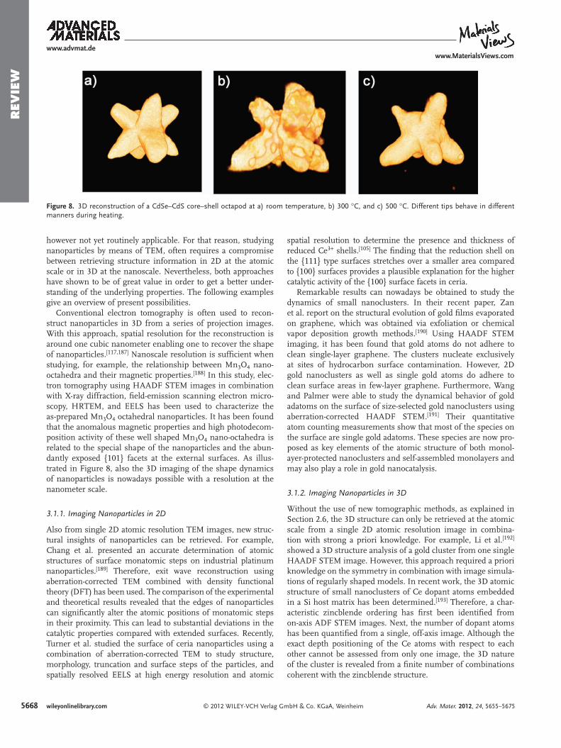
When incorporating nanomaterials in actual devices, they will be exposed to environmental conditions. It is therefore of great interest to perform dynamical 3D studies (e.g., as a function of temperature or when applying strain) by electron tomography as well. Especially for catalysis or optoelectronics, nanoparticle shape dynamics plays an important role. In order to reach these goals, further optimization of tomography holders and recon-struction algorithms will be required. Morphology changes that occur for a branched semiconductor nanostructure, having blunt and sharp tips, were investigated by ex situ heating and the results are illustrated in Figure 8 . 3D experiments in which heating is performed in situ are soon expected. [ 186 ]
3. Materials Applications
3.1. Imaging of Nanoparticles
Determining the 3D atomic structure of nanoparticles, quantita-tively and with high precision, is a challenging problem. Recent techniques to reach this goal, as discussed in Section 2.6, are
5667wileyonlinelibrary.combH & Co. KGaA, Weinheim
5668
www.advmat.dewww.MaterialsViews.com
REV
IEW
Figure 8 . 3D reconstruction of a CdSe–CdS core–shell octapod at a) room temperature, b) 300 ° C, and c) 500 ° C. Different tips behave in different manners during heating.
however not yet routinely applicable. For that reason, studying nanoparticles by means of TEM, often requires a compromise between retrieving structure information in 2D at the atomic scale or in 3D at the nanoscale. Nevertheless, both approaches have shown to be of great value in order to get a better under-standing of the underlying properties. The following examples give an overview of present possibilities.
Conventional electron tomography is often used to recon-struct nanoparticles in 3D from a series of projection images. With this approach, spatial resolution for the reconstruction is around one cubic nanometer enabling one to recover the shape of nanoparticles. [ 117 , 187 ] Nanoscale resolution is suffi cient when studying, for example, the relationship between Mn 3 O 4 nano-octahedra and their magnetic properties. [ 188 ] In this study, elec-tron tomography using HAADF STEM images in combination with X-ray diffraction, fi eld-emission scanning electron micro-scopy, HRTEM, and EELS has been used to characterize the as-prepared Mn 3 O 4 octahedral nanoparticles. It has been found that the anomalous magnetic properties and high photodecom-position activity of these well shaped Mn 3 O 4 nano-octahedra is related to the special shape of the nanoparticles and the abun-dantly exposed {101} facets at the external surfaces. As illus-trated in Figure 8 , also the 3D imaging of the shape dynamics of nanoparticles is nowadays possible with a resolution at the nanometer scale.
3.1.1. Imaging Nanoparticles in 2D
Also from single 2D atomic resolution TEM images, new struc-tural insights of nanoparticles can be retrieved. For example, Chang et al. presented an accurate determination of atomic structures of surface monatomic steps on industrial platinum nanoparticles. [ 189 ] Therefore, exit wave reconstruction using aberration-corrected TEM combined with density functional theory (DFT) has been used. The comparison of the experimental and theoretical results revealed that the edges of nanoparticles can signifi cantly alter the atomic positions of monatomic steps in their proximity. This can lead to substantial deviations in the catalytic properties compared with extended surfaces. Recently, Turner et al. studied the surface of ceria nanoparticles using a combination of aberration-corrected TEM to study structure, morphology, truncation and surface steps of the particles, and spatially resolved EELS at high energy resolution and atomic
wileyonlinelibrary.com © 2012 WILEY-VCH Verlag G
spatial resolution to determine the presence and thickness of reduced Ce 3 + shells. [ 105 ] The fi nding that the reduction shell on the {111} type surfaces stretches over a smaller area compared to {100} surfaces provides a plausible explanation for the higher catalytic activity of the {100} surface facets in ceria.
Remarkable results can nowadays be obtained to study the dynamics of small nanoclusters. In their recent paper, Zan et al. report on the structural evolution of gold fi lms evaporated on graphene, which was obtained via exfoliation or chemical vapor deposition growth methods. [ 190 ] Using HAADF STEM imaging, it has been found that gold atoms do not adhere to clean single-layer graphene. The clusters nucleate exclusively at sites of hydrocarbon surface contamination. However, 2D gold nanoclusters as well as single gold atoms do adhere to clean surface areas in few-layer graphene. Furthermore, Wang and Palmer were able to study the dynamical behavior of gold adatoms on the surface of size-selected gold nanoclusters using aberration-corrected HAADF STEM. [ 191 ] Their quantitative atom counting measurements show that most of the species on the surface are single gold adatoms. These species are now pro-posed as key elements of the atomic structure of both monol-ayer-protected nanoclusters and self-assembled monolayers and may also play a role in gold nanocatalysis.
3.1.2. Imaging Nanoparticles in 3D
Without the use of new tomographic methods, as explained in Section 2.6, the 3D structure can only be retrieved at the atomic scale from a single 2D atomic resolution image in combina-tion with strong a priori knowledge. For example, Li et al. [ 192 ] showed a 3D structure analysis of a gold cluster from one single HAADF STEM image. However, this approach required a priori knowledge on the symmetry in combination with image simula-tions of regularly shaped models. In recent work, the 3D atomic structure of small nanoclusters of Ce dopant atoms embedded in a Si host matrix has been determined. [ 193 ] Therefore, a char-acteristic zincblende ordering has fi rst been identifi ed from on-axis ADF STEM images. Next, the number of dopant atoms has been quantifi ed from a single, off-axis image. Although the exact depth positioning of the Ce atoms with respect to each other cannot be assessed from only one image, the 3D nature of the cluster is revealed from a fi nite number of combinations coherent with the zincblende structure.
mbH & Co. KGaA, Weinheim Adv. Mater. 2012, 24, 5655–5675

www.advmat.dewww.MaterialsViews.com
REV
IEW
Figure 9 . HAADF STEM image of a PbSe–CdSe core–shell structure acquired along the [110] zone axis of PbSe and CdSe. Columns of Pb, Se, and Cd can be clearly distinguished. Further-more, the Pb columns show clear variations in intensity indicating different numbers of Pb atoms/column. By combining counting results from the [110], [100], and [010] zone axis, the Pb lattice forming the core has been reconstructed in 3D with atomic resolution.
As shown in Section 2.6.3, novel techniques have been developed to extract quantitative 3D atomic scale informa-tion from a limited number of 2D projected on-axis HAADF STEM images. [ 13 ] This technique has initially been applied to metal nanocrystals embedded in a stabilizing matrix with the same crystal structure. However, the technique is more gen-erally applicable and can also be used to study, for example, free-standing, colloidal core–shell semiconductor nanocrystals that are much less stable and easily rotate during examination with an electron beam. [ 15 ] Colloidal, core–shell, semiconductor nanocrystals form an important class of optoelectronic mate-rials. Further progress in optoelectrical engineering will there-fore depend on a quantitative characterization and thorough understanding of the structure at the atomic scale with special focus on the interfaces. Rod-shaped PbSe(core)–CdSe(shell) hetero-nanocrystals obtained by Cd-for-Pb cation-exchange have been studied, starting from PbSe nanocrystal seeds. Revealing the complete atomic structure is essential to gain further under-standing of the mechanism of cation exchange at the nanoscale and the chemistry of the PbSe–CdSe interfaces. Figure 9 shows a PbSe(core)–CdSe(shell) particle imaged along the [110] direc-tion using aberration-corrected HAADF STEM. Because of the Z 2 –dependence of the contrast, the core and shell can clearly be distinguished. We remark here that PbSe has a rocksalt crystal structure, whereas the CdSe shell formed by ion-exchange is zincblende. Using the atom counting procedure discussed in Section 2.1, the number of Pb atoms in the core could be quan-tifi ed in each projected atomic column. By combining counting results from the [110], [100], and [010] zone axes, the Pb lattice forming the core has been reconstructed in 3D with atomic resolution. The lower row of Figure 9 shows the resulting reconstruction along different viewing directions. Surprisingly,
© 2012 WILEY-VCH Verlag GmbH & Co. KGaA, WeinhAdv. Mater. 2012, 24, 5655–5675
the symmetry of the core is different from what could be expected based on a single 2D image and incomplete Pb-planes at the interface are observed. The 3D analysis also revealed that cation exchange during growth proceeds in a layer-by-layer fashion along cer-tain crystallographic planes. The speed of the exchange depends on the directions in the crystal. Clearly these studies provide com-pletely novel insights.
3.1.3. Small, Smaller, Smallest
Ultrasmall nanoparticles or clusters, having sizes below 1 nm, form a challenging subject of investigation. Especially, the characteriza-tion of their structure is far from straight-forward. At the same time however, there is a clear need for a complete characterization in 3D since these materials can no longer be considered to be periodic objects. One of the main bottlenecks is that these clus-ters may rotate or show structural changes during investigation by TEM. [ 192 ] Obvi-ously, conventional electron tomography methods, even those that are based on a lim-ited number of projections, can no longer
be applied. On the other hand, the intrinsic energy transfer from the electron beam to the cluster can be considered as a unique possibility to investigate the transformation between energetically excited confi gurations of the same cluster. This idea was exploited in a recent study in which the dynamical behaviour of ultrasmall Ge clusters, consisting of less than 25 atoms, was investigated. 2D image series were collected using aberration-corrected HAADF STEM and selected frames were analyzed using statistical parameter estimation theory. In this manner, the number of atoms at each position could be determined as illustrated in Figure 10 . In order to extract 3D structural information from these images without using prior knowledge on the structure, ab initio calculations were carried out. Several starting confi gurations were constructed that are all in agreement with the experimental 2D projection images. Although all of the cluster confi gurations stay relatively close to their starting structure after full relaxation, only those con-fi gurations in which a planar base structure was assumed, were found to be still compatible with the 2D experimental images. In this manner, reliable 3D structural models are obtained for these small clusters and also the transformation of a predominantly 2D confi guration into a compact 3D con-fi guration could be characterized.
3.2. The Fine Structure of Interfaces
Interfaces play an important role in materials science and nanotechnology. For example, with the discovery of new high T c superconductors in materials such as YBa 2 Cu 3 O 7 , the rele-vance of twin interfaces and domain boundaries became par-ticularly important. [ 194 ] As twin interfaces, domain boundaries
5669wileyonlinelibrary.comeim

5670
www.advmat.dewww.MaterialsViews.com
REV
IEW
Figure 10 . The top row presents the statistical counting results for 3 different confi gurations of an ultrasmall Ge cluster. Green, red and blue dots correspond to 1, 2 and 3 atoms respectively. The results of the ab-initio calculations are shown at the bottom.
or antiphase boundaries are not necessarily a structural juxtaposition of bulk materials, they are able to locally change the properties of a bulk material. Typical examples of this effect are superconducting domain boundaries in insulating materials, [ 195 ] the presence of a two-dimensional electron gas restricted to interfaces [ 109,110 , 196 ] or multiferroicity at domain boundaries. [ 197 ] All these properties are related either to slight atom shifts or slight composition changes at the interface. Aberration-corrected TEM, HAADF STEM, and STEM EELS have been used in numerous studies to investigate such effects in complex oxide materials. [ 39 , 87 , 198 ] As an example, we will illus-trate this for the “simple” case of CaTiO 3 where ferrielectricity has been directly observed at ferroelastic twin boundaries. [ 37 ] Numerical calculations have shown that domain boundaries in CaTiO 3 are mainly ferrielectric with maximum dipole moments at the wall.
wileyonlinelibrary.com © 2012 WILEY-VCH Verlag
Figure 11 . a) Experimental phase image of a {110} twin boundary in orthcenter of the four neighboring Ca atomic columns are indicated by green ato the twin wall averaged along and in mirror operation with respect to the
Twin boundaries of the {110} type in orthorhombic CaTiO 3 (space group Pnma ) have recently been imaged along [001] using aberration-corrected TEM in combination with exit wave recon-struction. The phase of the reconstructed exit wave is shown in Figure 11 a with a resolution equal to 0.8 Å. This phase is directly proportional to the projected electrostatic potential of the struc-ture. In order to obtain quantitative numbers for the atomic column positions, techniques such as statistical parameter estimation need to be included. This allows position measure-ments of all atomic columns with a precision of a few picom-eters without being restricted by the information limit of the microscope. In order to quantify the atomic column positions, statistical parameter estimation theory has been used. [ 24,25 , 36 ] Using this approach, the phase of the reconstructed exit wave is considered as a data plane from which the atomic column positions are estimated in a statistical way. The key to successful
GmbH & Co. KGaA, Weinheim
orhombic CaTiO 3 . Mean displacements of the Ti atomic columns from the rrows. b,c) Displacements of Ti atomic columns perpendicular and parallel twin wall together with their 90% confi dence intervals.
Adv. Mater. 2012, 24, 5655–5675
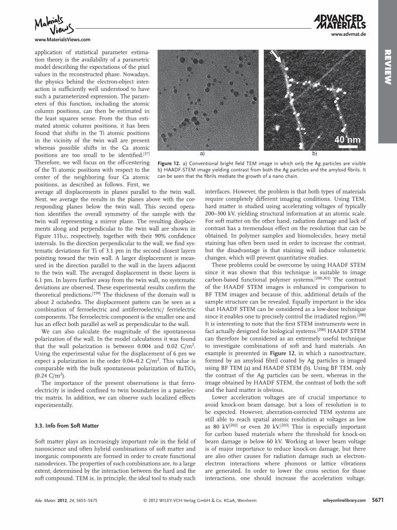
www.advmat.dewww.MaterialsViews.com
REV
IEW
Figure 12 . a) Conventional bright fi eld TEM image in which only the Ag particles are visible b) HAADF-STEM image yielding contrast from both the Ag particles and the amyloid fi brils. It can be seen that the fi brils mediate the growth of a nano chain.
application of statistical parameter estima-tion theory is the availability of a parametric model describing the expectations of the pixel values in the reconstructed phase. Nowadays, the physics behind the electron-object inter-action is suffi ciently well understood to have such a parameterized expression. The param-eters of this function, including the atomic column positions, can then be estimated in the least squares sense. From the thus esti-mated atomic column positions, it has been found that shifts in the Ti atomic positions in the vicinity of the twin wall are present whereas possible shifts in the Ca atomic positions are too small to be identifi ed. [ 37 ] Therefore, we will focus on the off-centering of the Ti atomic positions with respect to the center of the neighboring four Ca atomic positions, as described as follows. First, we
average all displacements in planes parallel to the twin wall. Next, we average the results in the planes above with the cor-responding planes below the twin wall. This second opera-tion identifi es the overall symmetry of the sample with the twin wall representing a mirror plane. The resulting displace-ments along and perpendicular to the twin wall are shown in Figure 11 b,c, respectively, together with their 90% confi dence intervals. In the direction perpendicular to the wall, we fi nd sys-tematic deviations for Ti of 3.1 pm in the second closest layers pointing toward the twin wall. A larger displacement is meas-ured in the direction parallel to the wall in the layers adjacent to the twin wall. The averaged displacement in these layers is 6.1 pm. In layers further away from the twin wall, no systematic deviations are observed. These experimental results confi rm the theoretical predictions. [ 199 ] The thickness of the domain wall is about 2 octahedra. The displacement pattern can be seen as a combination of ferroelectric and antiferroelectric/ ferrielectric components. The ferroelectric component is the smaller one and has an effect both parallel as well as perpendicular to the wall.We can also calculate the magnitude of the spontaneous polarization of the wall. In the model calculations it was found that the wall polarization is between 0.004 and 0.02 C/m 2 . Using the experimental value for the displacement of 6 pm we expect a polarization in the order 0.04–0.2 C/m 2 . This value is comparable with the bulk spontaneous polarization of BaTiO 3 (0.24 C/m 2 ).
The importance of the present observations is that ferro-electricity is indeed confi ned to twin boundaries in a paraelec-tric matrix. In addition, we can observe such localized effects experimentally.
3.3. Info from Soft Matter
Soft matter plays an increasingly important role in the fi eld of nanoscience and often hybrid combinations of soft matter and inorganic components are formed in order to create functional nanodevices. The properties of such combinations are, to a large extent, determined by the interaction between the hard and the soft compound. TEM is, in principle, the ideal tool to study such
© 2012 WILEY-VCH Verlag GmAdv. Mater. 2012, 24, 5655–5675
interfaces. However, the problem is that both types of materials require completely different imaging conditions. Using TEM, hard matter is studied using accelerating voltages of typically 200–300 kV, yielding structural information at an atomic scale. For soft matter on the other hand, radiation damage and lack of contrast has a tremendous effect on the resolution that can be obtained. In polymer samples and biomolecules, heavy metal staining has often been used in order to increase the contrast, but the disadvantage is that staining will induce volumetric changes, which will prevent quantitative studies.
These problems could be overcome by using HAADF STEM since it was shown that this technique is suitable to image carbon-based functional polymer systems. [ 200,201 ] The contrast of the HAADF STEM images is enhanced in comparison to BF TEM images and because of this, additional details of the sample structure can be revealed. Equally important is the idea that HAADF STEM can be considered as a low-dose technique since it enables one to precisely control the irradiated region. [ 200 ] It is interesting to note that the fi rst STEM instruments were in fact actually designed for biological systems. [ 200 ] HAADF STEM can therefore be considered as an extremely useful technique to investigate combinations of soft and hard materials. An example is presented in Figure 12 , in which a nanostructure, formed by an amyloid fi bril coated by Ag particles is imaged using BF TEM (a) and HAADF STEM (b). Using BF TEM, only the contrast of the Ag particles can be seen, whereas in the image obtained by HAADF STEM, the contrast of both the soft and the hard matter is obvious.
Lower acceleration voltages are of crucial importance to avoid knock-on beam damage, but a loss of resolution is to be expected. However, aberration-corrected TEM systems are still able to reach spatial atomic resolution at voltages as low as 80 kV [ 202 ] or even 20 kV. [ 203 ] This is especially important for carbon based materials where the threshold for knock-on beam damage is below 60 kV. Working at lower beam voltage is of major importance to reduce knock-on damage, but there are also other causes for radiation damage such as electron-electron interactions where phonons or lattice vibrations are generated. In order to lower the cross section for those interactions, one should increase the acceleration voltage.
5671wileyonlinelibrary.combH & Co. KGaA, Weinheim

5672
www.advmat.dewww.MaterialsViews.com
REV
IEW
Nevertheless, protein-like polymers were successfully imagedat 80 kV. [ 204 ] In some classes of soft matter, radiation damage is caused by a combination of knock-on damage and ionization damage. It is therefore not always straightforward to eliminate radiation damage completely. An additional advantage of using low voltage electrons for EELS measurements is the removal of relativistic effects, leading to a much more straightforward interpretation of the spectra. [ 205 ]
In many cases, it is required to investigate soft materials in 3D because their structure is often of an aperiodic nature. The fi rst applications of electron tomography in materials science were indeed carried out for porous materials. [ 206 ] For micro-meter thick polymer samples, low convergence angle STEM was found to be of great use. This approach enables to inves-tigate volumes larger than 10 μ m 3 . For such studies, a large number of images of the same area of interest needs to be recorded and the problem of beam damage is even more impor-tant. Reducing the electron dose during acquisition is therefore a key factor. Advanced reconstruction algorithms, such as the ones presented in Section 2.4.2, may also be an option to over-come this problem. [ 159 , 163 ] Currently, cryo-electron tomography is a very important technique to perform 3D imaging of soft materials. [ 207 ] Also for 2D studies, cryo-TEM can be considered as being one of the most valuable techniques to study systems that combine biology and materials science. [ 208 ] Not only the effect of beam damage can be reduced by cryo-TEM, but also chemical fi xation and dehydration can be avoided since the samples are embedded in a thin layer of vitreous ice.
4. Conclusions
In this Review, the latest possibilities in the fi eld of electron microscopy have been discussed. During recent years, the elec-tron microscope has evolved from a powerful magnifying instru-ment towards a versatile, quantum mechanical measuring tool. Structural, but also chemical, electronic and magnetic informa-tion can be obtained at the atomic scale. These experiments can not only be carried out in 2D, but also 3D analyses are currently becoming standard. As demonstrated in this Review, the char-acterization limits are no longer imposed by the quality of the lenses but are determined by the underlying physical princi-ples. As we have illustrated, all of these developments provide exciting new prospects for solving a broad range of materials science problems, including the quantitative characterization of interfaces in oxide materials and hard-soft matter combinations as well as 3D investigations of nanoparticles at the atomic scale. Clearly, advanced electron microscopy will take characteriza-tion of advanced materials to the ultimate atomic level. This will lead to a better understanding and optimization of existing materials as well as the design of new structures with desired properties.
Acknowledgements This work was supported by funding from the European Research Council under the 7 th Framework Program (FP7), ERC grant N ° 246791 - COUNTATOMS. J.V. Acknowledges funding from the European Research Council under the 7 th Framework Program (FP7), ERC Starting Grant
wileyonlinelibrary.com © 2012 WILEY-VCH Verlag
278510 VORTEX. The authors gratefully acknowledge funding from the Research Foundation Flanders (FWO, Belgium). The Qu-Ant-EM microscope was partly funded by the Hercules Fund from the Flemish Government. We thank Rafal Dunin-Borkowski for providing Figure 5 d. The authors would like to thank the colleagues who have contributed to this work over the years, including K.J. Batenburg, R. Erni, B. Goris, F. Leroux, H. Lichte, A. Lubk, B. Partoens, M.D. Rossell, P. Schattschneider, B. Schoeters, D. Schryvers, H. Tan, H. Tian, S. Turner, M. van Huis.
Received: May 25, 2012Published online: August 21, 2012
[ 1 ] E. Abbe , Arch. f. Mikroskop. Anat. 1873 , 9 , 413. [ 2 ] E. Abbe , in Gesammelte Abhandlungen (Ed. S. Czapski) ,
G. Fischer Verlag, Jena Germany 1904 , pp 1 – 508 . [ 3 ] E. Ruska , Biosci. Rep. 1987 , 7 , 607. [ 4 ] J. W. Menter , Proc. R. Soc. London, Ser. A 1956 , 236 , 119 . [ 5 ] H. Formanek , M. Muller , M. H. Hahn , T. Koller , Naturwissenschaften
1971 , 58 , 339 . [ 6 ] F. P. Ottensme , E. E. Schmidt , J. Powell , T. Jack , J. Ultrastruct. Res.
1972 , 40 , 546 . [ 7 ] H. Hashimot , A. Kumao , K. Hino , H. Yotsumot , A. Ono , Jpn. J.
Appl. Phys. 1971 , 10 , 1115 . [ 8 ] A. V. Crewe , J. Wall , J. Langmore , Science 1970 , 168 , 1338 . [ 9 ] S. Iijima , Acta Crystallogr. A 1973 , 29 , 18 . [ 10 ] S. Iijima , J. G. Allpress , J. Solid. State. Chem. 1973 , 7 , 94 . [ 11 ] M. Haider , S. Uhlemann , E. Schwan , H. Rose , B. Kabius , K. Urban ,
Nature 1998 , 392 , 768 . [ 12 ] K. W. Urban , Science 2008 , 321 , 506 . [ 13 ] S. Van Aert , K. J. Batenburg , M. D. Rossell , R. Erni , G. Van Ten-
deloo , Nature 2011 , 470 , 374 . [ 14 ] a) M. C. Scott , C. C. Chen , M. Mecklenburg , C. Zhu , R. Xu , P. Ercius ,
U. Dahmen , B. C. Regan , J. W. Miao , Nature 2012 , 483 , 444 ; b) D. Van Dyck , F. R. Chen , Nature 2012 , 483 , 444 ; c) S. Bals , S. Van Aert , C. Romero , K. Lauwaet , M. J. Van Bael , B. Sch-oeters , B. Partoens , E. Yucelen , P. Lievens , G. Van Tendeloo , Nat. Commun. 2012 , DOI: 10.1038/ncomms1887.
[ 15 ] S. Bals , M. Casavola , M. A. van Huis , S. Van Aert , K. J. Batenburg , G. Van Tendeloo , D. Vanmaekelbergh , Nano. Lett. 2011 , 11 , 3420 .
[ 16 ] G. Van Tendeloo , D. Van Dyck , in Handbook of Nanoscopy (Eds: G. Van Tendeloo , D. Van Dyck , S. J. Pennycook ), Wiley-VCH Verlag , Weinheim 2012 .
[ 17 ] U. Dahmen , R. Erni , V. Radmilovic , C. Kisielowski , M. D. Rossell , P. Denes , Philos. Trans. R. Soc. A 2009 , 367 , 3795 .
[ 18 ] H. Rose , Optik 1990 , 85 , 19 . [ 19 ] D. Van Dyck , S. Van Aert , A. J. den Dekker , A. van den Bos , Ultra-
microscopy 2003 , 98 , 27 . [ 20 ] a) D. A. Muller , Ultramicroscopy 1999 , 78 , 163 ; b) C. Kisielowski ,
E. Principe , B. Freitag , D. Hubert , Physica B 2001 , 308 , 1090 . [ 21 ] J. P. Locquet , J. Perret , J. Fompeyrine , E. Machler , J. W. Seo ,
G. Van Tendeloo , Nature 1998 , 394 , 453 . [ 22 ] L. Rayleigh in Scientifi c Papers , Vol. 3 (Eds: J. W. Strutt , L. Rayleigh ),
Cambridge University Press , Cambridge 1902 , 47 . [ 23 ] M. A. Okeefe , Ultramicroscopy 1992 , 47 , 282 . [ 24 ] A. J. den Dekker , S. Van Aert , A. van den Bos , D. Van Dyck , Ultra-
microscopy 2005 , 104 , 83 . [ 25 ] S. Van Aert , A. J. den Dekker , A. van den Bos , D. Van Dyck ,
J. H. Chen , Ultramicroscopy 2005 , 104 , 107 . [ 26 ] E. Bettens , D. Van Dyck , A. J. den Dekker , J. Sijbers , A. van den
Bos , Ultramicroscopy 1999 , 77 , 37 . [ 27 ] S. Van Aert , A. J. den Dekker , D. Van Dyck , A. van den Bos , J. Struct.
Biol. 2002 , 138 , 21 .
GmbH & Co. KGaA, Weinheim Adv. Mater. 2012, 24, 5655–5675

www.advmat.dewww.MaterialsViews.com
REV
IEW
[ 28 ] P. E. Batson , N. Dellby , O. L. Krivanek , Nature 2002 , 419 , 94 . [ 29 ] D. Vandyck , W. Coene , Optik 1987 , 77 , 125 . [ 30 ] Q. Fu , H. Lichte , E. Volkl , Phys. Rev. Lett. 1991 , 67 , 2319 . [ 31 ] A. I. Kirkland , W. O. Saxton , K. L. Chau , K. Tsuno , M. Kawasaki ,
Ultramicroscopy 1995 , 57 , 355 . [ 32 ] W. Coene , G. Janssen , M. O. Debeeck , D. Vandyck , Phys. Rev. Lett.
1992 , 69 , 3743 . [ 33 ] C. Kisielowski , C. J. D. Hetherington , Y. C. Wang , R. Kilaas ,
M. A. O’Keefe , A. Thust , Ultramicroscopy 2001 , 89 , 243 . [ 34 ] C. L. Jia , A. Thust , Phys. Rev. Lett. 1999 , 82 , 5052 . [ 35 ] J. Ayache , C. Kisielowski , R. Kilaas , G. Passerieux ,
S. Lartigue-Korinek , J. Mater. Sci. 2005 , 40 , 3091 . [ 36 ] S. Bals , S. Van Aert , G. Van Tendeloo , D. Avila-Brande , Phys. Rev.
Lett. 2006 , 96 , 096106 . [ 37 ] S. Van Aert , S. Turner , R. Delville , D. Schryvers , G. Van Tendeloo ,
E. K. H. Salje , Adv. Mater. 2012 , 24 , 523 . [ 38 ] a) C. L. Jia , M. Lentzen , K. Urban , Science 2003 , 299 , 870 ;
b) C. L. Jia , L. Houben , A. Thust , J. Barthel , Ultramicroscopy 2010 , 110 , 500 .
[ 39 ] C. L. Jia , S. B. Mi , K. Urban , I. Vrejoiu , M. Alexe , D. Hesse , Nat. Mater. 2008 , 7 , 57 .
[ 40 ] C. L. Jia , S. B. Mi , K. Urban , I. Vrejoiu , M. Alexe , D. Hesse , Phys. Rev. Lett. 2009 , 102 , 117601 .
[ 41 ] C. L. Jia , S. B. Mi , M. Faley , U. Poppe , J. Schubert , K. Urban , Phys. Rev. B 2009 , 79 , 081405 .
[ 42 ] J. M. Cowley , M. S. Hansen , S. Y. Wang , Ultramicroscopy 1995 , 58 , 18 .
[ 43 ] P. D. Nellist , S. J. Pennycook , Phys. Rev. Lett. 1998 , 81 , 4156 . [ 44 ] R. Erni , M. D. Rossell , C. Kisielowski , U. Dahmen , Phys. Rev. Lett.
2009 , 102 , 096101 . [ 45 ] S. Van Aert , J. Verbeeck , R. Erni , S. Bals , M. Luysberg , D. Van Dyck ,
G. Van Tendeloo , Ultramicroscopy 2009 , 109 , 1236 . [ 46 ] S. D. Findlay , N. Shibata , H. Sawada , E. Okunishi , Y. Kondo ,
T. Yamamoto , Y. Ikuhara , Appl. Phys. Lett. 2009 , 95 , 191913 . [ 47 ] S. D. Findlay , N. Shibata , H. Sawada , E. Okunishi , Y. Kondo ,
Y. Ikuhara , Ultramicroscopy 2010 , 110 , 903 . [ 48 ] S. D. Findlay , T. Saito , N. Shibata , Y. Sato , J. Matsuda , K. Asano ,
E. Akiba , T. Hirayama , Y. Ikuhara , Appl. Phys. Express 2010 , 3 , 116603 .
[ 49 ] R. Ishikawa , E. Okunishi , H. Sawada , Y. Kondo , F. Hosokawa , E. Abe , Nat. Mater. 2011 , 10 , 278 .
[ 50 ] R. Huang , T. Hitosugi , S. D. Findlay , C. A. J. Fisher , Y. H. Ikuhara , H. Moriwake , H. Oki , Y. Ikuhara , Appl. Phys. Lett. 2011 , 98 , 051913 .
[ 51 ] M. J. Hytch , W. M. Stobbs , Ultramicroscopy 1994 , 53 , 191 . [ 52 ] C. B. Boothroyd , Ultramicroscopy 2000 , 83 , 159 . [ 53 ] C. B. Boothroyd , R. E. Dunin-Borkowski , Ultramicroscopy 2004 , 98 ,
115 . [ 54 ] A. Thust , Phys. Rev. Lett. 2009 , 102 , 220801 . [ 55 ] D. O. Klenov , S. Stemmer , Ultramicroscopy 2006 , 106 , 889 . [ 56 ] J. M. LeBeau , A. J. D’Alfonso , S. D. Findlay , S. Stemmer , L. J. Allen ,
Phys. Rev. B 2009 , 80 , 174106 . [ 57 ] J. M. LeBeau , S. D. Findlay , L. J. Allen , S. Stemmer , Phys. Rev. Lett.
2008 , 100 , 206101 . [ 58 ] C. Dwyer , R. Erni , J. Etheridge , Ultramicroscopy 2010 , 110 , 952 . [ 59 ] A. Rosenauer , K. Gries , K. Muller , A. Pretorius , M. Schowalter ,
A. Avramescu , K. Engl , S. Lutgen , Ultramicroscopy 2009 , 109 , 1171 .
[ 60 ] T. Niermann , A. Lubk , F. Röder , Ultramicroscopy 2012 , 115 , 68 . [ 61 ] A. Lubk , F. Röder , T. Niermann , C. Gatel , S. Joulie , F. Houdellier ,
C. Magen , M. Hÿtch , Ultramicroscopy 2012 , 115 , 78 . [ 62 ] C. Dwyer , Ultramicroscopy 2010 , 110 , 195 . [ 63 ] E. H. Darlington , T. G. Sparrow , J. Phys. E Sci. Instrum. 1975 , 8 ,
596 . [ 64 ] H. Rose , E. Plies , Optik 1974 , 40 , 336 .
© 2012 WILEY-VCH Verlag GAdv. Mater. 2012, 24, 5655–5675
[ 65 ] R. Castaing , L. Henry , C. R. Hebd. Seanc. Acad. Sci. 1962 , 255 , 76 . [ 66 ] S. Uhlemann , H. Rose , Optik 1994 , 96 , 163 . [ 67 ] K. Tsuno , E. Munro , Rev. Sci. Instrum. 1997 , 68 , 109 . [ 68 ] Y. Bando , M. Mitome , D. Goldberg, Y. Kitami , K. Kurashima ,
T. Kaneyama , Y. Okura , M. Naruse , Jpn. J. Appl. Phys. 2001 , 40 , 1193 .
[ 69 ] A. Gubbens , M. Barfels , C. Trevor , R. Twesten , P. Mooney , P. Thomas , N. Menon , B. Kraus , C. Mao , B. McGinn , Ultramicros-copy 2010 , 110 , 962 .
[ 70 ] H. Sawada , Y. Tanishiro , N. Ohashi , T. Tomita , F. Hosokawa , T. Kaneyama , Y. Kondo , K. Takayanagi , J. Electron Microsc. 2009 , 58 , 357 .
[ 71 ] N. Dellby , N. J. Bacon , P. Hrncirik , M. F. Murfi tt , G. S. Skone , Z. S. Szilagyi , O. L. Krivanek , Eur. Phys. J.-Appl. Phys. 2011 , 54 , 33505 .
[ 72 ] F. Houdellier , A. l. Masseboeuf , M. Monthioux , M. J. Hytch , Carbon 2012 , 50 , 2037 .
[ 73 ] T. Isabell , J. Brink , M. Kawasaki , B. Armbruster , I. Ishikawa , E. Okunishi , H. Sawada , Y. Okura , K. Yamazaki , T. Ishikawa , M. Kawazu , M. Hori , M. Terao , M. Kanno , S. Tanba , Y. Kondo , Microscopy Today 2009 , 17 , 8 .
[ 74 ] H. W. Mook , P. Kruit , Ultramicroscopy 2000 , 81 , 129 . [ 75 ] K. Tsuno , Nucl. Instrum. Meth. A 2011 , 645 , 12 . [ 76 ] O. L. Krivanek , J. P. Ursin , N. J. Bacon , G. J. Corbin , N. Dellby ,
P. Hrncirik , M. F. Murfi tt , C. S. Own , Z. S. Szilagyi , Philos. T. R. Soc. A 2009 , 367 , 3683 .
[ 77 ] a) I. Ishikawa , E. Okunishi , H. Sawada , Y. Okura , K. Yamazaki , T. Ishikawa , M. Kawazu , M. Hori , M. Terao , M. Kanno , S. Tanba , Y. Kondo , Microsc. Microanal. 2009 , 15 , 188 ; b) P. Schlossmacher , D. O. Klenov , B. Freitag , S. v. Harrach , A. Steinbach , Microsc. Micro-anal. 2010 , 24 , S5 .
[ 78 ] J. Verbeeck , S. Van Aert , Ultramicroscopy 2004 , 101 , 207 . [ 79 ] P. Cueva , R. Hovden , J. A. Mundy , H. L. Xin , D. A. Muller , Arxiv
2012 , arXiv:1112.3059v1. [ 80 ] J. Verbeeck , S. Van Aert , G. Bertoni , Ultramicroscopy 2006 , 106 ,
976 . [ 81 ] H. Shuman , A. P. Somlyo , Ultramicroscopy 1987 , 21 , 23 . [ 82 ] T. Manoubi , M. Tence , M. G. Walls , C. Colliex , Microsc. Microanal.
M 1990 , 1 , 23 . [ 83 ] R. D. Leapman , C. R. Swyt , Ultramicroscopy 1988 , 26 , 393 . [ 84 ] F. de la Pena , M. H. Berger , J. F. Hochepied , F. Dynys , O. Stephan ,
M. Walls , Ultramicroscopy 2011 , 111 , 169 . [ 85 ] C. Jeanguillaume , C. Colliex , Ultramicroscopy 1989 , 28 , 252 . [ 86 ] M. Bosman , V. J. Keast , J. L. Garcia-Munoz , A. J. D’Alfonso ,
S. D. Findlay , L. J. Allen , Phys. Rev. Lett. 2007 , 99 , 086102 . [ 87 ] D. A. Muller , L. F. Kourkoutis , M. Murfi tt , J. H. Song , H. Y. Hwang ,
J. Silcox , N. Dellby , O. L. Krivanek , Science 2008 , 319 , 1073 . [ 88 ] S. Lazar , Y. Shao , L. Gunawan , R. Nechache , A. Pignolet ,
G. A. Botton , Microsc. Microanal. 2010 , 16 , 416 . [ 89 ] A. J. D’Alfonso , B. Freitag , D. Klenov , L. J. Allen , Phys. Rev. B 2010 ,
81 , 100101 . [ 90 ] C. Dwyer , S. D. Findlay , L. J. Allen , Phys. Rev. B 2008 , 77 , 184107 . [ 91 ] P. Schattschneider , B. Jouffrey , M. Nelhiebel , Phys. Rev. B 1996 , 54 ,
3861 . [ 92 ] J. Verbeeck , P. Schattschneider , A. Rosenauer , Ultramicroscopy
2009 , 109 , 350 . [ 93 ] L. J. Allen , A. J. D’Alfonso , S. D. Findlay , J. M. LeBeau , N. R. Lugg ,
S. Stemmer , J. Phys. Conf. Ser. 2010 , 241 , 012061 . [ 94 ] L. J. Allen , A. J. D’Alfonso , S. D. Findlay , M. P. Oxley , M. Bosman ,
V. J. Keast , E. C. Cosgriff , G. Behan , P. D. Nellist , A. I. Kirkland , AIP Conf. Proc. 2008 , 999 , 32 .
[ 95 ] L. J. Allen , A. J. D’Alfonso , B. Freitag , D. O. Klenov , MRS Bull. 2012 , 37 , 47 .
[ 96 ] P. Wang , A. J. D’Alfonso , S. D. Findlay , L. J. Allen , A. L. Bleloch , Phys. Rev. Lett. 2008 , 101 , 236102 .
5673wileyonlinelibrary.commbH & Co. KGaA, Weinheim

5674
www.advmat.dewww.MaterialsViews.com
REV
IEW
[ 97 ] P. Schorsch , H. Rose , Eur. J. Cell Biol. 1997 , 74 , 84 .[ 98 ] K. Suenaga , M. Koshino , Nature 2010 , 468 , 1088 . [ 99 ] K. Suenaga , Y. Sato , Z. Liu , H. Kataura , T. Okazaki , K. Kimoto ,
H. Sawada , T. Sasaki , K. Omoto , T. Tomita , T. Kaneyama , Y. Kondo , Nat. Chem. 2009 , 1 , 415 .
[ 100 ] T. Haiyan , J. Verbeeck , A. Abakumov , G. Van Tendeloo , Ultramicros-copy 2012 , 116 , 24 .
[ 101 ] L. A. J. Garvie , A. J. Craven , Phys. Chem. Miner. 1994 , 21 , 191 . [ 102 ] C. Colliex , T. Manoubi , C. Orthiz , Phys. Rev. B 1991 , 44 , 11402 . [ 103 ] J. H. Rask , B. A. Miner , P. R. Buseck , Ultramicroscopy 1987 , 21 ,
321 . [ 104 ] A. Ohtomo , D. A. Muller , J. L. Grazul , H. Y. Hwang , Nature 2002 ,
419 , 378 . [ 105 ] S. Turner , S. Lazar , B. Freitag , R. Egoavil , J. Verbeeck , S. Put ,
Y. Strauven , G. Van Tendeloo , Nanoscale 2011 , 3 , 3385 . [ 106 ] H. T. Tan , S. Turner , E. Yucelen , J. Verbeeck , G. Van Tendeloo , Phys.
Rev. Lett. 2011 , 107 , 107602 . [ 107 ] S. Turner , J. Verbeeck , F. Ramezanipour , J. E. Greedan ,
G. Van Tendeloo , Chem. Mater. 2012 , 24 , 1904 . [ 108 ] M. Coey , Nature 2004 , 430 , 155 . [ 109 ] A. Ohtomo , H. Y. Hwang , Nature 2004 , 427 , 423 . [ 110 ] M. Huijben , G. Rijnders , D. H. A. Blank , S. Bals , S. Van Aert ,
J. Verbeeck , G. Van Tendeloo , A. Brinkman , H. Hilgenkamp , Nat. Mater. 2006 , 5 , 556 .
[ 111 ] R. F. Egerton , Rep. Prog. Phys. 2009 , 72 , 016502 . [ 112 ] M. O. Krause , J. H. Oliver , J. Phys. Chem. Ref. Data 1979 , 8 , 329 . [ 113 ] Y. Aharonov , D. Bohm , Phys. Rev. 1959 , 115 , 485 . [ 114 ] J. N. Chapman , J. Phys. D Appl. Phys. 1984 , 17 , 623 . [ 115 ] S. McVitie , G. S. White , J. Scott , P. Warin , J. N. Chapman , J. Appl.
Phys. 2001 , 90 , 5220 . [ 116 ] K. Harada , T. Matsuda , J. Bonevich , M. Igarashi , S. Kondo ,
G. Pozzi , U. Kawabe , A. Tonomura , Nature 1992 , 360 , 51 . [ 117 ] P. A. Midgley , R. E. Dunin-Borkowski , Nat. Mater. 2009 , 8 , 271 . [ 118 ] H. Rose , Ultramicroscopy 1977 , 2 , 251 . [ 119 ] H. Rose , Optik 1974 , 39 , 416 . [ 120 ] N. H. Dekkers , H. D. Lang , Optik 1974 , 41 , 452 . [ 121 ] J. N. Chapman , P. E. Batson , E. M. Waddell , R. P. Ferrier , Ultrami-
croscopy 1978 , 3 , 203 . [ 122 ] D. Gabor , Science 1972 , 177 , 299 . [ 123 ] H. Lichte , M. Lehmann , Rep. Prog. Phys. 2008 , 71 , 016102 . [ 124 ] G. Mollenstedt , H. Duker , Z. Phys. 1956 , 145 , 377 . [ 125 ] a) M. Beleggia , T. Kasama , R. E. Dunin-Borkowski , Ultramicro-
scopy 2010 , 110 , 425 ; b) R. E. Dunin-Borkowski , B. Kardynal , M. R. McCartney , M. R. Scheinfein , D. J. Smith , Mater. Res. Soc. Symp. Proc. 2001 , 589 , 13 .
[ 126 ] C. Phatak , A. K. Petford-Long , M. De Graef , Phys. Rev. Lett. 2010 , 104 , 253901 .
[ 127 ] a) B. Freitag , S. Kujawa , M. Linck , D. Geiger , T. Niermann , M. Lehmann , H. Lichte , Microsc. Microanal. 2009 , 15 , 1098 ; b) H. Lichte , M. Linck , D. Geiger , M. Lehmann , Microsc. Microanal. 2010 , 16 , 434 .
[ 128 ] J. Sickmann , P. Formanek , M. Linck , U. Muehle , H. Lichte , Ultra-microscopy 2011 , 111 , 290 .
[ 129 ] M. Kuwahara , Y. Takeda , K. Saitoh , T. Ujihara , H. Asano , T. Nakanishi , N. Tanaka , J. Phys.: Conf. Ser. 2011 , 298 , 012016 .
[ 130 ] D. L. Abraham , H. Hopster , Phys. Rev. Lett. 1989 , 62 , 1157 . [ 131 ] J. Kirschner , D. Rebenstorff , H. Ibach , Phys. Rev. Lett. 1984 , 53 ,
698 . [ 132 ] C. Hebert , P. Schattschneider , Ultramicroscopy 2003 , 96 , 463 . [ 133 ] P. Schattschneider , S. Rubino , C. Hebert , J. Rusz , J. Kunes ,
P. Novak , E. Carlino , M. Fabrizioli , G. Panaccione , G. Rossi , Nature 2006 , 441 , 486 .
[ 134 ] G. Schutz , W. Wagner , W. Wilhelm , P. Kienle , R. Zeller , R. Frahm , G. Materlik , Phys. Rev. Lett. 1987 , 58 , 737 .
wileyonlinelibrary.com © 2012 WILEY-VCH Verlag G
[ 135 ] P. Schattschneider , I. Ennen , S. Loffl er , M. Stoger-Pollach , J. Verbeeck , J. Appl. Phys. 2010 , 107 , 09D311 .
[ 136 ] P. Schattschneider , M. Stoger-Pollach , S. Rubino , M. Sperl , C. Hurm , J. Zweck , J. Rusz , Phys. Rev. B 2008 , 78 , 104413 .
[ 137 ] J. Verbeeck , C. Hebert , S. Rubino , P. Novak , J. Rusz , F. Houdellier , C. Gatel , P. Schattschneider , Ultramicroscopy 2008 , 108 , 865 .
[ 138 ] P. Schattschneider , I. Ennen , M. Stoger-Pollach , J. Verbeeck , V. Mauchamp , M. Jaouen , Ultramicroscopy 2010 , 110 , 1038 .
[ 139 ] J. Verbeeck , P. Schattschneider , S. Lazar , M. Stoger-Pollach , S. Loffl er , A. Steiger-Thirsfeld , G. Van Tendeloo , Appl. Phys. Lett. 2011 , 99 , 203109 .
[ 140 ] J. Verbeeck , H. Tian , A. Béché , Ultramicroscopy 2012 , 113 , 83 . [ 141 ] B. Freitag , M. Bischoff , H. Mueller , P. Hartel , H. S. von Harrach ,
Microsc. Microanal. 2009 , 15 , 184 . [ 142 ] D. J. Derosier , A. Klug , Nature 1968 , 217 , 130 ; R. G. Hart , Science
1968 , 159 , 1464 . [ 143 ] W. Hoppe , R. Langer , G. Knesch , C. Poppe , Naturwissenschaften
1968 , 55 , 333 . [ 144 ] P. W. Hawkes , in Electron Tomography: Three-dimensional Imaging
with the Transmission Electron Microscope (Ed: J. Frank ), Plenum Press , New York 1992 .
[ 145 ] P. A. Midgley , M. Weyland , Ultramicroscopy 2003 , 96 , 413 . [ 146 ] G. Mobus , R. C. Doole , B. J. Inkson , Ultramicroscopy 2003 , 96 ,
433 . [ 147 ] R. A. Crowther , D. J. Derosier , A. Klug , Proc. R. Soc. London Ser. A
1970 , 317 , 319 . [ 148 ] P. Gilbert , J. Theor. Biol. 1972 , 36 , 105 . [ 149 ] H. Heidari Mezerji , W. Van den Broek , S. Bals , Ultramicroscopy
2011 , 111 , 330 . [ 150 ] M. Weyland , T. J. V. Yates , R. E. Dunin-Borkowski , L. Laffont ,
P. A. Midgley , Scripta Mater. 2006 , 55 , 29 . [ 151 ] a) I. Arslan , J. R. Tong , P. A. Midgley , Ultramicroscopy 2006 , 106 ,
994 ; b) J. Tong , I. Arslan , P. Midgley , J. Struct. Biol. 2006 , 153 , 55 . [ 152 ] N. Kawase , M. Kato , H. Nishioka , H. Jinnai , Ultramicroscopy 2007 ,
107 , 8 . [ 153 ] E. Biermans , L. Molina , K. J. Batenburg , S. Bals , G. Van Tendeloo ,
Nano Lett. 2010 , 10 , 5014 . [ 154 ] X. X. Ke , S. Bals , D. Cott , T. Hantschel , H. Bender , G. Van Tendeloo ,
Microsc. Microanal. 2010 , 16 , 210 . [ 155 ] a) H. Jinnai , Y. Nishikawa , R. J. Spontak , S. D. Smith , D. A. Agard ,
T. Hashimoto , Phys. Rev. Lett. 2000 , 84 , 518 ; b) Y. Ikeda , A. Katoh , J. Shimanuki , S. Kohjiya , Macromol. Rapid Commun. 2004 , 25 , 1186 ; c) L. Laffont , M. Weyland , R. Raja , J. M. Thomas , P. A. Midgley , Inst. Phys. Conf. Ser. 2004 , 179 , 459 .
[ 156 ] W. van Aarle , K. J. Batenburg , J. Sijbers , IEEE Trans. Med. Imaging 2011 , 30 , 980 .
[ 157 ] S. Bals , K. J. Batenburg , J. Verbeeck , J. Sijbers , G. Van Tendeloo , Nano Lett. 2007 , 7 , 3669 .
[ 158 ] K. J. Batenburg , S. Bals , J. Sijbers , C. Kubel , P. A. Midgley , J. C. Hernandez , U. Kaiser , E. R. Encina , E. A. Coronado , G. Van Tendeloo , Ultramicroscopy 2009 , 109 , 730 .
[ 159 ] S. Bals , K. J. Batenburg , D. D. Liang , O. Lebedev , G. Van Tendeloo , A. Aerts , J. A. Martens , C. E. A. Kirschhock , J. Am. Chem. Soc. 2009 , 131 , 4769 .
[ 160 ] L. Molina , H. Y. Tan , E. Biermans , K. J. Batenburg , J. Verbeeck , S. Bals , G. Van Tendeloo , Supercond. Sci. Technol. 2011 , 24 , 65019 .
[ 161 ] a) D. L. Donoho , IEEE Trans. Inform. Theory 2006 , 52 , 1289 ; b) D. L. Donoho , Commun. Pure Appl. Math. 2006 , 59 , 907 ; c) B. Goris , W. Van den Broek , K. J. Batenburg , H. Heidari Mezerji , S. Bals , Ultramicroscopy 2012 , 113 , 120 ; d) Z. Saghi , D. J. Holland , R. Leary , A. Falqui , G. Bertoni , A. J. Sederman , L. F. Gladden , P. A. Midgley , Nano Lett. 2011 , 11 , 4666 .
[ 162 ] B. Goris , T. Roelandts , J. Batenburg , H. Heidari Mezerji , S. Bals , Ultramicroscopy 2012 , DOI: 10.1016/j.ultramic.2012.07.003.
mbH & Co. KGaA, Weinheim Adv. Mater. 2012, 24, 5655–5675

www.advmat.dewww.MaterialsViews.com
REV
IEW
[ 163 ] F. Leroux , M. Gysemans , S. Bals , K. J. Batenburg , J. Snauwaert , T. Verbiest , C. Van Haesendonck , G. Van Tendeloo , Adv. Mater. 2010 , 22 , 2193 .
[ 164 ] M. Bar Sadan , L. Houben , S. G. Wolf , A. Enyashin , G. Seifert , R. Tenne , K. Urban , Nano Lett. 2008 , 8 , 891 .
[ 165 ] Z. Saghi , X. J. Xu , G. Mobus , J. Appl. Phys. 2009 , 106 , 24304 . [ 166 ] J. R. Jinschek , K. J. Batenburg , H. A. Calderon , R. Kilaas ,
V. Radmilovic , C. Kisielowski , Ultramicroscopy 2008 , 108 , 589 . [ 167 ] L. Houben , M. Bar Sadan , Ultramicroscopy 2011 , 111 , 1512 . [ 168 ] K. van Benthem , A. R. Lupini , M. Kim , H. S. Baik , S. Doh , J. H. Lee ,
M. P. Oxley , S. D. Findlay , L. J. Allen , J. T. Luck , S. J. Pennycook , Appl. Phys. Lett. 2005 , 87 , 034104 .
[ 169 ] H. L. L. Xin , D. A. Muller , Microsc. Microanal. 2009 , 15 , 1474 . [ 170 ] P. D. Nellist , G. Behan , A. I. Kirkland , C. J. D. Hetherington , Appl.
Phys. Lett. 2006 , 89 , 124105 . [ 171 ] E. C. Cosgriff , P. D. Nellist , A. J. D’Alfonso , S. D. Findlay , G. Behan ,
P. Wang , L. J. Allen , A. I. Kirkland , Adv. Imaging Electron Phys. 2010 , 162 , 45 .
[ 172 ] M. Takeguchi , A. Hashimoto , M. Shimojo , K. Mitsuishi , K. Furuya , J. Electron Microsc. 2008 , 57 , 123 .
[ 173 ] P. Wang , G. Behan , M. Takeguchi , A. Hashimoto , K. Mitsuishi , M. Shimojo , A. I. Kirkland , P. D. Nellist , Phys. Rev. Lett. 2010 , 104 , 200801 .
[ 174 ] P. Ercius , D. Muller , Microsc. Microanal. 2009 , 15 , 238 . [ 175 ] S. Bals , G. Van Tendeloo , C. Kisielowski , Adv. Mater. 2006 , 18 , 892 . [ 176 ] U. Kaiser , A. Chuvilin , Microsc. Microanal. 2003 , 9 , 36 . [ 177 ] J. M. Rebled , L. Yedra , S. Estrade , J. Portillo , F. Peiro , Ultramicros-
copy 2011 , 111 , 1504 . [ 178 ] J. S. Barnard , J. Sharp , J. R. Tong , P. A. Midgley , Science 2006 , 313 ,
319 . [ 179 ] a) B. Goris , S. Bals , W. Van den Broek , J. Verbeeck , G. Van Tendeloo ,
Ultramicroscopy 2011 , 111 , 1262 ; b) G. Mobus , B. J. Inkson , Mater. Today 2007 , 10 , 18 ; c) R. D. Leapman , E. Kocsis , G. Zhang , T. L. Talbot , P. Laquerriere , Ultramicroscopy 2004 , 100 , 115 .
[ 180 ] M. H. Gass , K. K. K. Koziol , A. H. Windle , P. A. Midgley , Nano Lett. 2006 , 6 , 376 .
[ 181 ] A. Yurtsever , M. Weyland , D. A. Muller , Appl. Phys. Lett. 2006 , 89 , 151920 .
[ 182 ] a) D. Wolf , A. Lubk , H. Lichte , H. Friedrich , Ultramicroscopy 2010 , 110 , 390 ; b) A. C. Twitchett-Harrison , T. J. V. Yates , S. B. Newcomb , R. E. Dunin-Borkowski , P. A. Midgley , Nano Lett. 2007 , 7 , 2020 .
[ 183 ] a) C. Phatak , M. Beleggia , M. De Graef , Ultramicroscopy 2008 , 108 , 503 ; b) S. J. Lade , D. Paganin , M. J. Morgan , Opt. Commun. 2005 , 253 , 392 .
[ 184 ] M. Hytch , F. Houdellier , F. Hue , E. Snoeck , Nature 2008 , 453 , 1086 .
[ 185 ] M. J. Hytch , E. Snoeck , R. Kilaas , Ultramicroscopy 1998 , 74 , 131 . [ 186 ] B. Goris , M. A. Van Huis , S. Bals , H. W. Zandbergen , L. Manna ,
G. Van Tendeloo , Small, 2012 , 8 , 937 . [ 187 ] I. Arslan , T. J. V. Yates , N. D. Browning , P. A. Midgley , Science 2005 ,
309 , 2195 .
© 2012 WILEY-VCH Verlag GAdv. Mater. 2012, 24, 5655–5675
[ 188 ] Y. Li , H. Y. Tan , X. Y. Yang , B. Goris , J. Verbeeck , S. Bals , P. Colson , R. Cloots , G. Van Tendeloo , B. L. Su , Small 2011 , 7 , 475 .
[ 189 ] L. Y. Chang , A. S. Barnard , L. C. Gontard , R. E. Dunin-Borkowski , Nano Lett. 2010 , 10 , 3073 .
[ 190 ] R. Zan , U. Bangert , Q. Ramasse , K. S. Novoselov , Small 2011 , 7 , 2868 .
[ 191 ] Z. W. Wang , R. E. Palmer , Nano Lett. 2012 , 12 , 91 . [ 192 ] Z. Y. Li , N. P. Young , M. Di Vece , S. Palomba , R. E. Palmer ,
A. L. Bleloch , B. C. Curley , R. L. Johnston , J. Jiang , J. Yuan , Nature 2008 , 451 , 46 .
[ 193 ] M. Couillard , G. Radtke , A. P. Knights , G. A. Botton , Phys. Rev. Lett. 2011 , 107 , 186104 .
[ 194 ] a) G. Van Tendeloo , D. Broddin , H. W. Zandbergen , S. Amelinckx , Physica C 1990 , 167 , 627 ; b) R. F. Klie , J. P. Buban , M. Varela , A. Franceschetti , C. Jooss , Y. Zhu , N. D. Browning , S. T. Pantelides , S. J. Pennycook , Nature 2005 , 435 , 475 .
[ 195 ] A. Aird , E. K. H. Salje , J. Phys.-Condens. Mater. 1998 , 10 , L377 . [ 196 ] N. Nakagawa , H. Y. Hwang , D. A. Muller , Nat. Mater. 2006 , 5 , 204 ;
C. L. Jia , S. B. Mi , M. Faley , U. Poppe , J. Schubert , K. Urban , Phys. Rev. B 2009 , 79 , 081405 .
[ 197 ] a) T. Lottermoser , M. Fiebig , Phys. Rev. B 2004 , 70 , 220407; b) G. Catalan , A. Lubk , A. H. G. Vlooswijk , E. Snoeck , C. Magen , A. Janssens , G. Rispens , G. Rijnders , D. H. A. Blank , B. Noheda , Nat. Mater. 2011 , 10 , 963 .
[ 198 ] M. Varela , T. J. Pennycook , W. Tian , D. Mandrus , S. J. Pennycook , V. Pena , Z. Sefrioui , J. Santamaria , J. Mater. Sci. 2006 , 41 , 4389 .
[ 199 ] L. Goncalves-Ferreira , S. A. T. Redfern , E. Artacho , E. K. H. Salje , Phys. Rev. Lett. 2008 , 101 , 097602 .
[ 200 ] E. Sourty , S. van Bavel , K. B. Lu , R. Guerra , G. Bar , J. Loos , Microsc. Microanal. 2009 , 15 , 251 .
[ 201 ] J. Loos , E. Sourty , K. B. Lu , G. de With , S. van Bavel , Macromol-ecules 2009 , 42 , 2581 .
[ 202 ] J. R. Jinschek , E. Yucelen , H. A. Calderon , B. Freitag , Carbon 2011 , 49 , 556 .
[ 203 ] U. Kaiser , J. Biskupek , J. C. Meyer , J. Leschner , L. Lechner , H. Rose , M. Stoger-Pollach , A. N. Khlobystov , P. Hartel , H. Muller , M. Haider , S. Eyhusen , G. Benner , Ultramicroscopy 2011 , 111 , 1239 .
[ 204 ] K. T. Nam , S. A. Shelby , P. H. Choi , A. B. Marciel , R. Chen , L. Tan , T. K. Chu , R. A. Mesch , B. C. Lee , M. D. Connolly , C. Kisielowski , R. N. Zuckermann , Nat. Mater. 2010 , 9 , 454 .
[ 205 ] M. Stoger-Pollach , A. Laister , P. Schattschneider , Ultramicroscopy 2008 , 108 , 439 .
[ 206 ] A. J. Koster , U. Ziese , A. J. Verkleij , A. H. Janssen , K. P. de Jong , J. Phys. Chem. B 2000 , 104 , 9368 .
[ 207 ] F. Nudelman , G. de With , N. A. J. M. Sommerdijk , Soft Matter 2011 , 7 , 17 .
[ 208 ] F. Nudelman , K. Pieterse , A. George , P. H. H. Bomans , H. Friedrich , L. J. Brylka , P. A. J. Hilbers , G. de With , N. A. J. M. Sommerdijk , Nat. Mater. 2010 , 9 , 1004 .
5675wileyonlinelibrary.commbH & Co. KGaA, Weinheim