Embed Size (px)
Citation preview

1FEATURES APPLICATIONS
DESCRIPTION
1
2
3
4
5
6
7
8
9 10
11
12
13
14
15
16
24
23
22
21
20
19
18
17
25
26
27
28
29
30
31
32
bq24721,bq24721C
CHGEN
ACDRV
ACN
ACP
ACDET
BYPASS
EAO
EAI
FB
O
AG
ND
VR
EF
5
VC
C
SD
A
SC
L
TS
ISY
NS
ET
IOUT
BAT
SRN
SRP
SYNN
SYNP
SYS
BATDRV
PV
CC
BT
ST
HID
RV
PH
RE
GN
LO
DR
V
PG
ND
AL
AR
M
5x5 QFN PACKAGE (TOP VIEW)
bq24721bq24721C
www.ti.com.................................................................................................................................................. SLUS683F–NOVEMBER 2005–REVISED APRIL 2009
ADVANCED MULTI-CHEMISTRY AND MULTI-CELL SYNCHRONOUS SWITCH-MODECHARGER AND SYSTEM POWER SELECTOR
• Portable Notebook Computers2• High Efficiency NMOS-NMOS SynchronousBuck Converter With User-Selectable 300 kHz • Portable DVD Playersor 500 kHz frequency • Webpads, PC Tablets
• bq24721C Offers Softer Turn-On, StrongerTurn-Off
• SBS-Like(1) SMBus Interface for Control and The bq24721 is a high efficiency synchronous batteryStatus Communications With Host pack charger with high level of integration for portable
applications. This device implements a high• Programmable Battery Voltage, Chargeperformance analog front-end that interfaces to theCurrent, and AC Adapter Current via SBS-Likesystem power management micro-controller throughSMBus Interface a simplified SBS-like SMBus interface.
• 0.4% Charge Voltage Regulation AccuracyThe dynamic power management (DPM) function• 3% Charge Current Regulation Accuracy modifies the charge current depending on system
• 3% Adapter Current Regulation Accuracy load conditions, avoiding ac adapter overload.Dynamic Power Management (DPM)
High accuracy current sense amplifiers enable• 2% Accuracy Integrated Charge and AC accurate measurement of either the charge current or
Adapter 20× Current Amplifier Output the ac adapter current, allowing termination ofnonsmart packs and monitoring of overall system• 3-Cell and 4-Cell Li-Ion Voltage Regulationpower.9 V, 12 V–14.4 V, 16 V–19.2 V
• Battery Pack Voltage Operating Range The adapter isolation diode can be bypassed or0 V–19.2 V entirely replaced with an external MOSFET using a
control signal provided by the bq24721, thus reducing• AC Adapter Operating Range 8 V–28 Voverall power dissipation.
• 99.5% Max Duty CycleIntegrated features such as charger soft start, charge• Internal Soft Startovercurrent protection, and IC temperature monitoring
• Integrated 5% 5-V LDO When AC Adapter provide a second level of protection, in addition toApplied pack and system protection functions.
• 6-V Drive Supply Voltage for IncreasedEfficiency
• Reverse Battery to Adapter DischargeProtection
• Battery/Adapter to System Power SelectorFunction
• Charge and Adapter Overcurrent Protection• Battery Thermistor Sense, TS, Comparators• Available in 32-Pin 5x5-mm QFN Package(1) SBS-Like interface is not 100% SBS compliant. SBS-Likeinterface is SMBus1.1 complaint but does not support Packet ErrorCorrection (PEC). The control and status registers were changedto simplify and enhance notebook charger control. An 8-bit address(0x12) is used. See Table 1 for a comparison between SBS-like vsSBS Specification.
1
Please be aware that an important notice concerning availability, standard warranty, and use in critical applications of TexasInstruments semiconductor products and disclaimers thereto appears at the end of this data sheet.
2PowerPAD is a trademark of Texas Instruments.
PRODUCTION DATA information is current as of publication date. Copyright © 2005–2009, Texas Instruments IncorporatedProducts conform to specifications per the terms of the TexasInstruments standard warranty. Production processing does notnecessarily include testing of all parameters.
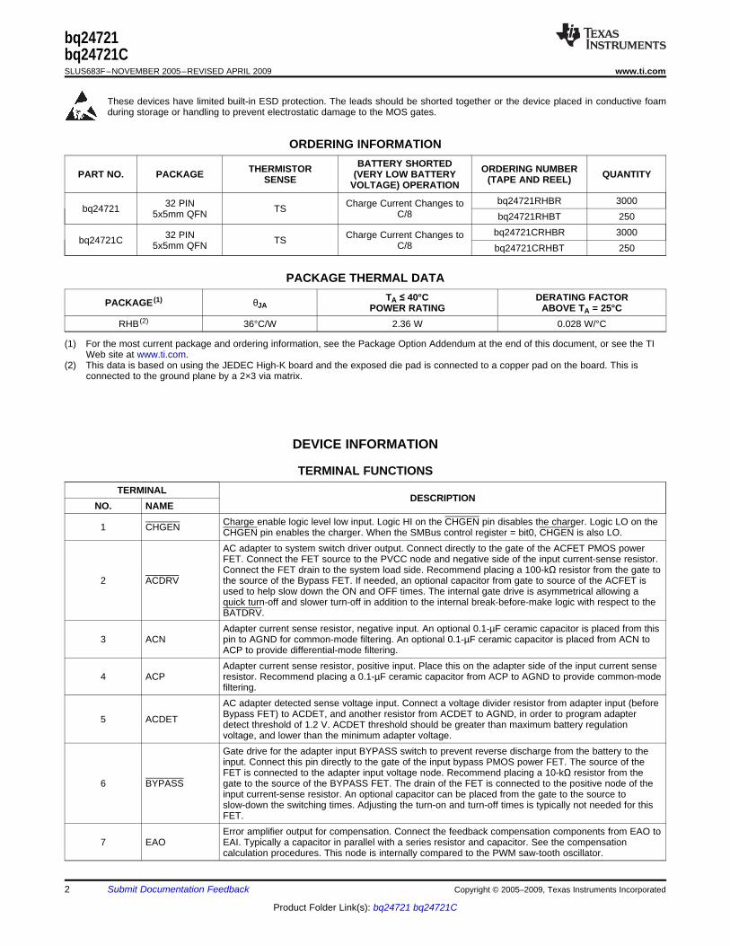
DEVICE INFORMATION
bq24721bq24721CSLUS683F–NOVEMBER 2005–REVISED APRIL 2009.................................................................................................................................................. www.ti.com
These devices have limited built-in ESD protection. The leads should be shorted together or the device placed in conductive foamduring storage or handling to prevent electrostatic damage to the MOS gates.
ORDERING INFORMATIONBATTERY SHORTEDTHERMISTOR ORDERING NUMBERPART NO. PACKAGE (VERY LOW BATTERY QUANTITYSENSE (TAPE AND REEL)VOLTAGE) OPERATION
bq24721RHBR 300032 PIN Charge Current Changes tobq24721 TS5x5mm QFN C/8 bq24721RHBT 250bq24721CRHBR 300032 PIN Charge Current Changes tobq24721C TS5x5mm QFN C/8 bq24721CRHBT 250
PACKAGE THERMAL DATATA ≤ 40°C DERATING FACTORPACKAGE (1) θJA POWER RATING ABOVE TA = 25°C
RHB (2) 36°C/W 2.36 W 0.028 W/°C
(1) For the most current package and ordering information, see the Package Option Addendum at the end of this document, or see the TIWeb site at www.ti.com.
(2) This data is based on using the JEDEC High-K board and the exposed die pad is connected to a copper pad on the board. This isconnected to the ground plane by a 2×3 via matrix.
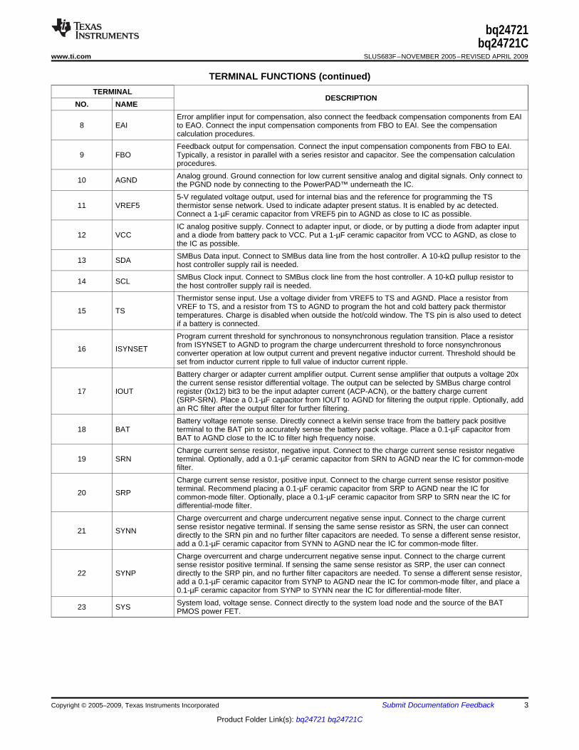
TERMINAL FUNCTIONSTERMINAL
DESCRIPTIONNO. NAME
Charge enable logic level low input. Logic HI on the CHGEN pin disables the charger. Logic LO on the1 CHGEN CHGEN pin enables the charger. When the SMBus control register = bit0, CHGEN is also LO.AC adapter to system switch driver output. Connect directly to the gate of the ACFET PMOS powerFET. Connect the FET source to the PVCC node and negative side of the input current-sense resistor.Connect the FET drain to the system load side. Recommend placing a 100-kΩ resistor from the gate to
2 ACDRV the source of the Bypass FET. If needed, an optional capacitor from gate to source of the ACFET isused to help slow down the ON and OFF times. The internal gate drive is asymmetrical allowing aquick turn-off and slower turn-off in addition to the internal break-before-make logic with respect to theBATDRV.Adapter current sense resistor, negative input. An optional 0.1-µF ceramic capacitor is placed from this
3 ACN pin to AGND for common-mode filtering. An optional 0.1-µF ceramic capacitor is placed from ACN toACP to provide differential-mode filtering.Adapter current sense resistor, positive input. Place this on the adapter side of the input current sense
4 ACP resistor. Recommend placing a 0.1-µF ceramic capacitor from ACP to AGND to provide common-modefiltering.AC adapter detected sense voltage input. Connect a voltage divider resistor from adapter input (beforeBypass FET) to ACDET, and another resistor from ACDET to AGND, in order to program adapter5 ACDET detect threshold of 1.2 V. ACDET threshold should be greater than maximum battery regulationvoltage, and lower than the minimum adapter voltage.Gate drive for the adapter input BYPASS switch to prevent reverse discharge from the battery to theinput. Connect this pin directly to the gate of the input bypass PMOS power FET. The source of theFET is connected to the adapter input voltage node. Recommend placing a 10-kΩ resistor from the
6 BYPASS gate to the source of the BYPASS FET. The drain of the FET is connected to the positive node of theinput current-sense resistor. An optional capacitor can be placed from the gate to the source toslow-down the switching times. Adjusting the turn-on and turn-off times is typically not needed for thisFET.Error amplifier output for compensation. Connect the feedback compensation components from EAO to
7 EAO EAI. Typically a capacitor in parallel with a series resistor and capacitor. See the compensationcalculation procedures. This node is internally compared to the PWM saw-tooth oscillator.
2 Submit Documentation Feedback Copyright © 2005–2009, Texas Instruments Incorporated
Product Folder Link(s): bq24721 bq24721C
bq24721bq24721C
www.ti.com.................................................................................................................................................. SLUS683F–NOVEMBER 2005–REVISED APRIL 2009
TERMINAL FUNCTIONS (continued)TERMINAL
DESCRIPTIONNO. NAME
Error amplifier input for compensation, also connect the feedback compensation components from EAI8 EAI to EAO. Connect the input compensation components from FBO to EAI. See the compensation
calculation procedures.Feedback output for compensation. Connect the input compensation components from FBO to EAI.
9 FBO Typically, a resistor in parallel with a series resistor and capacitor. See the compensation calculationprocedures.Analog ground. Ground connection for low current sensitive analog and digital signals. Only connect to10 AGND the PGND node by connecting to the PowerPAD™ underneath the IC.5-V regulated voltage output, used for internal bias and the reference for programming the TS
11 VREF5 thermistor sense network. Used to indicate adapter present status. It is enabled by ac detected.Connect a 1-µF ceramic capacitor from VREF5 pin to AGND as close to IC as possible.IC analog positive supply. Connect to adapter input, or diode, or by putting a diode from adapter input
12 VCC and a diode from battery pack to VCC. Put a 1-µF ceramic capacitor from VCC to AGND, as close tothe IC as possible.SMBus Data input. Connect to SMBus data line from the host controller. A 10-kΩ pullup resistor to the13 SDA host controller supply rail is needed.SMBus Clock input. Connect to SMBus clock line from the host controller. A 10-kΩ pullup resistor to14 SCL the host controller supply rail is needed.Thermistor sense input. Use a voltage divider from VREF5 to TS and AGND. Place a resistor fromVREF to TS, and a resistor from TS to AGND to program the hot and cold battery pack thermistor15 TS temperatures. Charge is disabled when outside the hot/cold window. The TS pin is also used to detectif a battery is connected.Program current threshold for synchronous to nonsynchronous regulation transition. Place a resistorfrom ISYNSET to AGND to program the charge undercurrent threshold to force nonsynchronous16 ISYNSET converter operation at low output current and prevent negative inductor current. Threshold should beset from inductor current ripple to full value of inductor current ripple.Battery charger or adapter current amplifier output. Current sense amplifier that outputs a voltage 20xthe current sense resistor differential voltage. The output can be selected by SMBus charge control
17 IOUT register (0x12) bit3 to be the input adapter current (ACP-ACN), or the battery charge current(SRP-SRN). Place a 0.1-µF capacitor from IOUT to AGND for filtering the output ripple. Optionally, addan RC filter after the output filter for further filtering.Battery voltage remote sense. Directly connect a kelvin sense trace from the battery pack positive
18 BAT terminal to the BAT pin to accurately sense the battery pack voltage. Place a 0.1-µF capacitor fromBAT to AGND close to the IC to filter high frequency noise.Charge current sense resistor, negative input. Connect to the charge current sense resistor negative
19 SRN terminal. Optionally, add a 0.1-µF ceramic capacitor from SRN to AGND near the IC for common-modefilter.Charge current sense resistor, positive input. Connect to the charge current sense resistor positiveterminal. Recommend placing a 0.1-µF ceramic capacitor from SRP to AGND near the IC for20 SRP common-mode filter. Optionally, place a 0.1-µF ceramic capacitor from SRP to SRN near the IC fordifferential-mode filter.Charge overcurrent and charge undercurrent negative sense input. Connect to the charge currentsense resistor negative terminal. If sensing the same sense resistor as SRN, the user can connect21 SYNN directly to the SRN pin and no further filter capacitors are needed. To sense a different sense resistor,add a 0.1-µF ceramic capacitor from SYNN to AGND near the IC for common-mode filter.Charge overcurrent and charge undercurrent negative sense input. Connect to the charge currentsense resistor positive terminal. If sensing the same sense resistor as SRP, the user can connect
22 SYNP directly to the SRP pin, and no further filter capacitors are needed. To sense a different sense resistor,add a 0.1-µF ceramic capacitor from SYNP to AGND near the IC for common-mode filter, and place a0.1-µF ceramic capacitor from SYNP to SYNN near the IC for differential-mode filter.System load, voltage sense. Connect directly to the system load node and the source of the BAT23 SYS PMOS power FET.
Copyright © 2005–2009, Texas Instruments Incorporated Submit Documentation Feedback 3
Product Folder Link(s): bq24721 bq24721C
bq24721bq24721CSLUS683F–NOVEMBER 2005–REVISED APRIL 2009.................................................................................................................................................. www.ti.com
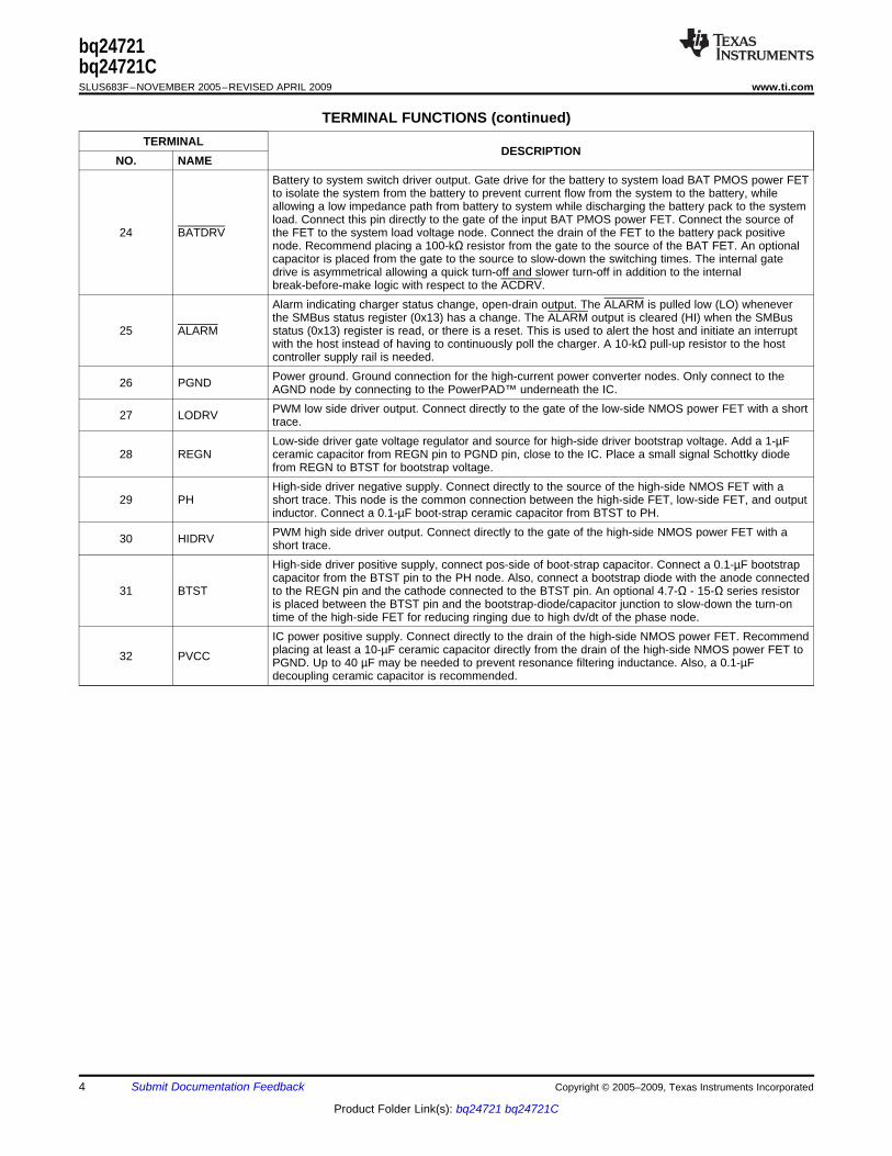
TERMINAL FUNCTIONS (continued)TERMINAL
DESCRIPTIONNO. NAME
Battery to system switch driver output. Gate drive for the battery to system load BAT PMOS power FETto isolate the system from the battery to prevent current flow from the system to the battery, whileallowing a low impedance path from battery to system while discharging the battery pack to the systemload. Connect this pin directly to the gate of the input BAT PMOS power FET. Connect the source of
24 BATDRV the FET to the system load voltage node. Connect the drain of the FET to the battery pack positivenode. Recommend placing a 100-kΩ resistor from the gate to the source of the BAT FET. An optionalcapacitor is placed from the gate to the source to slow-down the switching times. The internal gatedrive is asymmetrical allowing a quick turn-off and slower turn-off in addition to the internalbreak-before-make logic with respect to the ACDRV.Alarm indicating charger status change, open-drain output. The ALARM is pulled low (LO) wheneverthe SMBus status register (0x13) has a change. The ALARM output is cleared (HI) when the SMBus
25 ALARM status (0x13) register is read, or there is a reset. This is used to alert the host and initiate an interruptwith the host instead of having to continuously poll the charger. A 10-kΩ pull-up resistor to the hostcontroller supply rail is needed.Power ground. Ground connection for the high-current power converter nodes. Only connect to the26 PGND AGND node by connecting to the PowerPAD™ underneath the IC.PWM low side driver output. Connect directly to the gate of the low-side NMOS power FET with a short27 LODRV trace.Low-side driver gate voltage regulator and source for high-side driver bootstrap voltage. Add a 1-µF
28 REGN ceramic capacitor from REGN pin to PGND pin, close to the IC. Place a small signal Schottky diodefrom REGN to BTST for bootstrap voltage.High-side driver negative supply. Connect directly to the source of the high-side NMOS FET with a
29 PH short trace. This node is the common connection between the high-side FET, low-side FET, and outputinductor. Connect a 0.1-µF boot-strap ceramic capacitor from BTST to PH.PWM high side driver output. Connect directly to the gate of the high-side NMOS power FET with a30 HIDRV short trace.High-side driver positive supply, connect pos-side of boot-strap capacitor. Connect a 0.1-µF bootstrapcapacitor from the BTST pin to the PH node. Also, connect a bootstrap diode with the anode connected
31 BTST to the REGN pin and the cathode connected to the BTST pin. An optional 4.7-Ω - 15-Ω series resistoris placed between the BTST pin and the bootstrap-diode/capacitor junction to slow-down the turn-ontime of the high-side FET for reducing ringing due to high dv/dt of the phase node.IC power positive supply. Connect directly to the drain of the high-side NMOS power FET. Recommendplacing at least a 10-µF ceramic capacitor directly from the drain of the high-side NMOS power FET to32 PVCC PGND. Up to 40 µF may be needed to prevent resonance filtering inductance. Also, a 0.1-µFdecoupling ceramic capacitor is recommended.
4 Submit Documentation Feedback Copyright © 2005–2009, Texas Instruments Incorporated
Product Folder Link(s): bq24721 bq24721C
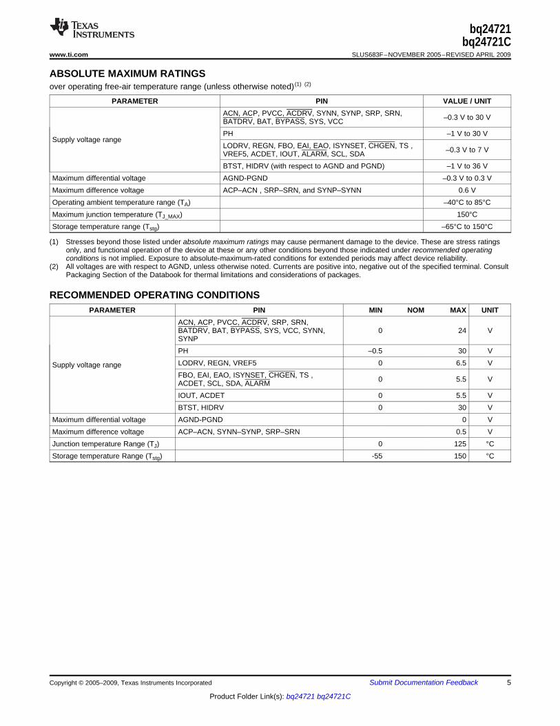
ABSOLUTE MAXIMUM RATINGS
RECOMMENDED OPERATING CONDITIONS
bq24721bq24721C
www.ti.com.................................................................................................................................................. SLUS683F–NOVEMBER 2005–REVISED APRIL 2009
over operating free-air temperature range (unless otherwise noted) (1) (2)
PARAMETER PIN VALUE / UNITACN, ACP, PVCC, ACDRV, SYNN, SYNP, SRP, SRN, –0.3 V to 30 VBATDRV, BAT, BYPASS, SYS, VCCPH –1 V to 30 V
Supply voltage rangeLODRV, REGN, FBO, EAI, EAO, ISYNSET, CHGEN, TS , –0.3 V to 7 VVREF5, ACDET, IOUT, ALARM, SCL, SDABTST, HIDRV (with respect to AGND and PGND) –1 V to 36 V
Maximum differential voltage AGND-PGND –0.3 V to 0.3 VMaximum difference voltage ACP–ACN , SRP–SRN, and SYNP–SYNN 0.6 VOperating ambient temperature range (TA) –40°C to 85°CMaximum junction temperature (TJ_MAX) 150°CStorage temperature range (Tstg) –65°C to 150°C
(1) Stresses beyond those listed under absolute maximum ratings may cause permanent damage to the device. These are stress ratingsonly, and functional operation of the device at these or any other conditions beyond those indicated under recommended operatingconditions is not implied. Exposure to absolute-maximum-rated conditions for extended periods may affect device reliability.
(2) All voltages are with respect to AGND, unless otherwise noted. Currents are positive into, negative out of the specified terminal. ConsultPackaging Section of the Databook for thermal limitations and considerations of packages.
PARAMETER PIN MIN NOM MAX UNITACN, ACP, PVCC, ACDRV, SRP, SRN,BATDRV, BAT, BYPASS, SYS, VCC, SYNN, 0 24 VSYNPPH –0.5 30 VLODRV, REGN, VREF5 0 6.5 VSupply voltage rangeFBO, EAI, EAO, ISYNSET, CHGEN, TS , 0 5.5 VACDET, SCL, SDA, ALARMIOUT, ACDET 0 5.5 VBTST, HIDRV 0 30 V
Maximum differential voltage AGND-PGND 0 VMaximum difference voltage ACP–ACN, SYNN–SYNP, SRP–SRN 0.5 VJunction temperature Range (TJ) 0 125 °CStorage temperature Range (Tstg) -55 150 °C
Copyright © 2005–2009, Texas Instruments Incorporated Submit Documentation Feedback 5
Product Folder Link(s): bq24721 bq24721C
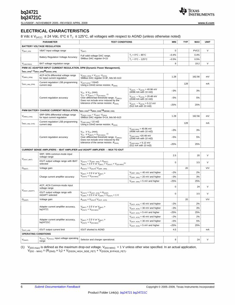
ELECTRICAL CHARACTERISTICS
bq24721bq24721CSLUS683F–NOVEMBER 2005–REVISED APRIL 2009.................................................................................................................................................. www.ti.com
8 Vdc ≤ V(VCC) ≤ 24 Vdc, 0°C ≤ TJ ≤ 125°C, all voltages with respect to AGND (unless otherwise noted)PARAMETER TEST CONDITIONS MIN TYP MAX UNIT
BATTERY VOLTAGE REGULATION
V(BAT_ICR) VBAT Input voltage range V(BAT) 0 PVCC V
TJ = 0°C – 85°C –0.4% 0.4%Full valid voltage DAC range,Battery Regulation Voltage Accuracy SMBus DAC register 0×15 TJ = 0°C – 125°C –0.5% 0.5%
V(VBATREG) BAT voltage regulation range 9 19.2 V
PWM AC ADAPTER INPUT CURRENT REGULATION, DPM (Dynamic Power Management),I(REG_DPM)= V(IREG_DPM)/R(SENSE_DPM)
ACP-ACN differential voltage range V(IREG_DPM) = V(ACP)- V(ACN)V(IREG_DPM) 1.28 162.56 mVfor input current regulation SMBus DAC register 0×3F, bits b0–b13
Current regulation LSB programming V(ACP-ACN) / 10mΩI(REG_step_DPM) 128 mAcurrent step Using a 10mΩ sense resistor, R(SNS)
V(ACP) – V(ACN) > 40.96 mV –3% 3%(4096 mA with 10 mΩ)VCC ≥ VCC (min),VCC ≥ VI(BAT) + V(DO-MAX), (1)
V(ACP) – V(ACN) > 20.48 mVCurrent regulation accuracy Over differential threshold range, V(IREG), –5% 5%(2048 mA with 10 mΩ)Does not include error induced by thetolerance of the sense resistor, R(SNS) V(ACP) – V(ACN) > 5.12 mV –25% 25%(512 mA with 10 mΩ)
PWM BATTERY CHARGE CURRENT REGULATION, I(REG_CHG)= V(IREG_CHG)/ R(SENSE_CHG)
SRP-SRN differential voltage range V(IREG_CHG) = V(SRP)- V(SRN)V(IREG_CHG) 1.28 162.56 mVfor input current regulation SMBus DAC register 0×14, bits b0–b13
Current regulation LSB programming V(SRP-SRN) / 10 mΩI(REG_step_CHG) 128 mAcurrent step Using a 10mΩ sense resistor, R(SNS)
V(SRP-SRN) > 40.96 mV –3% 3%(4096 mA with 10 mΩ)VCC ≥ VCC (min),VCC ≥ VI(BAT) + V(DO-MAX), (1)
V(SRP-SRN) >20.48 mVCurrent regulation accuracy Over differential threshold range, V(IREG), –5% 5%(2048 mA with 10 mΩ)Does not include error induced by thetolerance of the sense resistor, R(SNS) V(SRP-SRN) > 5.12 mV –25% 25%(512 mA with 10 mΩ)
CURRENT SENSE AMPLIFIERS – IBAT AMPLIFIER and IADAPT AMPLIFIER → MUX TO IOUT
SRP, SRN common-mode input 2.5 20 Vvoltage rangeV(IOUT_IBAT)
IOUT output voltage range with IBAT V(IOUT) = V(SRP, SRN) × A(IBAT) 0 3.5 Vselected V(BAT) > 2.5 V or V(BAT) > V(IOUT) + V(DO-MAX)(1)
G(IBAT) Voltage gain A(IOUT) = V(IOUT)/ V(SRP, SRN) 20 V/V
V(SRP, SRN) = 40 mV and higher –2% 2%V(BAT) > 2.5 V or V(BAT) >V(IOUT) + V(DO-MAX)
(1)Charge current amplifier accuracy V(SRP, SRN) = 20 mV and higher –3% 3%
V(SRP, SRN) = 5 mV and higher –25% 25%
ACP, ACN Common-mode input 0 24 Vvoltage rangeV(IOUT_IADAPT)
IOUT output voltage range with V(IOUT) = V(ACP, ACN) × A(IADP) 0 3.5 VIADAPT selected V(SRP) > 2.5 V or V(SRP) > V(IOUT) + 1 V
G(IADP) Voltage gain A(IADP) = V(IOUT)/ V(ACP, ACN) 20 V/V
V(ACP, ACN) = 40 mV and higher –2% 2%Adapter current amplifier accuracy, V(BAT) > 2.5 V or V(BAT) > V(ACP, ACN) = 30 mV and higher –3% 3%bq24721 V(IOUT) + V(DO-MAX)
(1)
V(ACP, ACN) = 5 mV and higher –25% 25%
V(ACP, ACN) = 40 mV and higher –2% 2%Adapter current amplifier accuracy, V(BAT) > 2.5 V or V(BAT) > V(ACP, ACN) = 30 mV and higher –5% 5%bq24721C V(IOUT) + V(DO-MAX)
(1)
V(ACP, ACN) = 5 mV and higher –25% 25%
I(OUT_LIM) IOUT output current limit IOUT shorted to AGND 4.5 mA
OPERATING CONDITIONS
V(VCC), V(PVCC), input voltage operatingV(INOP) Selector and charger operational. 8 24 Vrange
(1) V(DO-max) is defined as the maximum drop-out voltage. V(DO-MAX) = 1 V unless other wise specified. In an actual application,V(DO - MAX) = (R(SNS) × IO) + V(DSON_HIGH_SIDE_FET) + V(DSON_BYPASS_FET).
6 Submit Documentation Feedback Copyright © 2005–2009, Texas Instruments Incorporated
Product Folder Link(s): bq24721 bq24721C

bq24721bq24721C
www.ti.com.................................................................................................................................................. SLUS683F–NOVEMBER 2005–REVISED APRIL 2009
ELECTRICAL CHARACTERISTICS (continued)8 Vdc ≤ V(VCC) ≤ 24 Vdc, 0°C ≤ TJ ≤ 125°C, all voltages with respect to AGND (unless otherwise noted)
PARAMETER TEST CONDITIONS MIN TYP MAX UNIT
QUIESCENT CURRENT – NO ADAPTER CONNECTED
I(VCC,PVCC) VCC and PVCC quiescent current I(VCC,PVCC) = ( I(VCC) + I(PVCC) ) at V(VCC) = V(PVCC) = 16.8 V 254 µA
I(ACP,ACN) ACP and ACN quiescent current I(ACP,ACN) = ( I(ACP) + I(ACN) ) at V(ACP) = V(ACN) = V(VCC) = V(PVCC) = 16.8 V 1 µA
I(BAT) BAT quiescent current I(BAT) at V(BAT) = V(VCC) = V(PVCC) = 16.8 V 17 µA
I(SRP,SRN) SRP and SRN quiescent current I(SRP,SRN) = ( I(SRP) + I(SRN) ) at V(SRP) = V(SRN) = V(VCC) = V(PVCC) = 16.8 V 1 µA
I(SYNN,SYNP) SYNN and SYNP quiescent current I(SYNN,SYNP) = ( I(SYNN) + I(SYNP) ) at V(SYNP) = V(SYNN) = V(VCC) = V(PVCC) = 16.8 V 1 µA
I(SYS) SYS quiescent current I(SYS) at V(SYS) = V(VCC) = V(PVCC) = 16.8 V 25 µA
I(PH) PH quiescent current I(PH) at V(PH) = V(VCC) = V(PVCC) = 16.8 V 1 µA
I(BTST) BTST quiescent current I(BTST) at V(BTST) = V(VCC) = V(PVCC) = 16.8 V 1 µA
QUIESCENT CURRENT – ADAPTER CONNECTED AND READY TO CHARGE
I(VCC,PVCC) VCC and PVCC quiescent current I(VCC,PVCC) = (I(VCC) + I(PVCC) at V(VCC) = V(PVCC) = 16.8 V 4.45 mA
I(ACP,ACN) ACP and ACN quiescent current I(ACP,ACN) = (I(ACP) + I(ACN) ) at V(ACP) = V(ACN) = V(VCC) = V(PVCC) = 16.8 V 815 µA
I(BAT) BAT quiescent current I(BAT) at V(BAT) = V(VCC) = V(PVCC) = 16.8 V 500 µA
I(SRP,SRN) SRP and SRN quiescent current I(SRP,SRN) = ( I(SRP) + I(SRN) ) at V(SRP) = V(SRN) = V(VCC) = V(PVCC) = 16.8 V 305 µA
SYNN, SYNP, and SYS quiescent I(SYNN,SYNP,SYS) = ( I(SYNN) + I(SYNP) + I(SYS) ) at V(SYNP) = V(SYNN) = V(SYS) = V(VCC) =I(SYNN,SYNP,SYS) 321 µAcurrent V(PVCC) = 16.8 V
I(PH) PH quiescent current I(PH) at V(PH) = V(VCC) = V(PVCC) = 16.8 V 1 µA
I(BTST) BTST quiescent current I(BTST) at V(BTST) = V(VCC) = V(PVCC) = 16.8 V 1 µA
I(VCC_SW) = I(VCC)FPWM = 300 kHz, charger on (CHGEN = LO) = ENABLEDVCC Current while converter isI(VCC_SW) Q(G) at HIDRV = Q(G) at LODRV = 30 nC, [No Load on VREF5] 25 mAswitching including gate drive current Gate drive switching current = Q(G) × FPWM = (30nC + 30nC) × 300kHz =18mA
5-V REFERENCE LDO VOLTAGE AND AC DETECTION STATUS (VREF5, TURNS ON WHEN AC DETECTED)
Adapter detected (VACDET >V(ACD)), VCC> 7 VV(VREF5) 5V Regulator output voltage 4.75 5 5.25 V0 → 10 mA, source current
Adapter not detected, (VACDET< V(ACD))V(VREF5_SAT) Saturation voltage when VREF5 is off 0.3 V0 → –10 mA, ac adapter inserted, CO = 1 µF, discharge Load
I(VREF5_LIM) Short-circuit current V(VREF5) = AGND 20 mA
UNDERVOLTAGE LOCKOUT CIRCUIT
Undervoltage lockout threshold VREF5 rising, POR mode set at VREF5 < V(UVLO) 3.7 VUVLO
V(UVLO) hysteresis VREF5 falling 100 mV
SBS-Like SMBus LOGIC LEVELS
VIL Input low threshold level 2.7 V < V(pull-up) < 5.5 V, SDA and SCL 0.8 V
VIH Input high threshold level 2.7 V < V(pull-up) < 5.5 V, SDA and SCL 2.1 V
I(bias) Input bias current 2.7 V < V(pull-up) < 5.5 V, SDA and SCL 1 µA
ALARM OPEN DRAIN OUTPUT
V(ALARM_sat) ALARM output low saturation level I(ALARM) = 5mA 0.5 V
Ilkg(ALARM) ALARM leakage current V(ALARM) = 5V 1 µA
THERMAL SHUTDOWN, IC OVERTEMPERATURE PROTECTION
T(SHUT) Thermal shutdown Threshold TJ rising, Charge disabled at TJ > T(SHUT) 145 °C
T(SHUTH) Hysteresis TJ falling, Charge enabled at TJ < T(SHUT) – T(SHUTH) 15 °C
Deglitch time, thermal shutdown TJ rising/falling 8 ms
Copyright © 2005–2009, Texas Instruments Incorporated Submit Documentation Feedback 7
Product Folder Link(s): bq24721 bq24721C
bq24721bq24721CSLUS683F–NOVEMBER 2005–REVISED APRIL 2009.................................................................................................................................................. www.ti.com
ELECTRICAL CHARACTERISTICS (continued)8 Vdc ≤ V(VCC) ≤ 24 Vdc, 0°C ≤ TJ ≤ 125°C, all voltages with respect to AGND (unless otherwise noted)
PARAMETER TEST CONDITIONS MIN TYP MAX UNIT
THERMISTOR COMPARATORS, TS
Cold temperature threshold, TS pinV(LTF) V(TS) rising 72.8 73.5 74.2 %VREF5voltage
V(LTFH) Hysteresis for LTF threshold V(TS) falling 0.5 1 1.5 %VREF5
Cutoff temperature threshold, TS pinV(TCO) V(TS) rising 28.7 29.3 29.9 %VREF5voltage
Hot temperature threshold, TS pinV(HTF) V(TS) rising/falling 33.7 34.4 35.1 %VREF5voltage
V(TSDET) Pack thermistor insertion detected VT(S) rising/falling 82.45 85 87.55 %VREF5
Deglitch time for temperature out of V(TS) rising above V(LTF), or V(TS) falling below V(TCO) , or V(TS) falling below V(HTF) 16 µsrange detection
Deglitch time for temperature in valid V(TS) falling below (V(LTF) - V(LTFH)), or V(TS) rising above V(TCO) , or V(TS) rising 8 msrange detection above V(HTF)
Deglitch time for thermistor removal V(TS) rising above V(TSDET) 16 µsdetection V(TS) > V(TSDET) (pack removed)
Deglitch time for thermistor insertion V(TS) falling below V(TSDET) 1 sdetection V(TS) < V(TSDET) (pack inserted)
CHARGE OVERCURRENT COMPARATOR
V(SYNP-SYNN) rising,V(OLP) Overcurrent protection threshold 170 200 250 %I(REG_CHG)V(BAT) = 12.4 V, V(IREG–CHG) DAC programmed to 81.92 mV
V(OLPH) Hysteresis V(SYNP-SYNN) falling 20 %I(REG_CHG)
Deglitch time V(SYNP-SYNN) rising and falling 1 µs
SYNCHRONOUS to NONSYNCHRONOUS CURRENT COMPARATOR (ISYNSET)
V(SYNSET) ISYNSET pin set voltage 1 V
V(SYNP-SYNN) falling,K(SYNSET) ISYNSET current set factor 500 V/AISYN_NSYN= (V(SYNSET) × K(SYNSET))/(R(SYNSET) × R(SENSE_CHG))
V(SYN_HYS) V(SYNP-SYNN) hysteresis voltage, rising V(SYNP-SYNN) rising 1.5 mV
Deglitch time, Synch to Non-Synch V(SYNP-SYNN) rising and falling 1 µs
ADAPTER OVERCURRENT COMPARATOR (ACOC)
V(ACP-ACN) ≥ V(ACOC) , where SMBus charge mode register (0×12), % of110 130 155b6 = 1 = ACOC_protection_enabled, b8 = 0, b7 = 0 I(REG_DPM)
V(ACP-ACN) ≥ V(ACOC) , where SMBus charge mode register (0×12), % of130 150 175b6 = 1 = ACOC_protection_enabled, b8 = 0, b7 = 1 I(REG_DPM)ACOC Input over-current protectionV(ACOC) sense resistor voltage threshold V(ACP-ACN) ≥ V(ACOC) , where SMBus charge mode register (0×12), % of150 170 195b6 = 1 = ACOC_protection_enabled, b8 = 1, b7 = 0 I(REG_DPM)
V(ACP-ACN) ≥ V(ACOC) , where SMBus charge mode register (0×12), % of170 190 215b6 1 = ACOC_protection_enabled, b8 = 1, b7 = 1 I(REG_DPM)
V(ACOCH) ACOC Hysteresis V(SRP-SRN) falling 7 %I(REG_CHG)
ACOC deglitch time before ACDRV V(ACP-ACN) rising 16 µsturns-off
ACOC delay time afterV(ACP-ACN)≤V(ACOC) before ACDRV V(ACP-ACN) falling, V(ACP-ACN)≤V(ACOC) 8 msturn-on
SYSTEM STATUS COMPARATORS INPUT SPECIFICATIONS
Common mode input range at pin: 0 5 VACDET
VICR Common mode input range at TS pin 0.5 VREF5 V
Common mode input voltage range 0 VCC Vat pins: BAT, SYS
Input bias currents at pins: ACDET,I(bias) 0.2 µATS, BATDEP, SYS
BATTERY DEPLETED COMPARATOR (BATDEP)
V(BATDEP) = 2.2 V + V(step) × batdep_dac_code, where batdep_dac_code = 0 - 7,and Vstep = 0.1V, SMBus Charge Mode register 0×12, bits b9, b10, b11
V(BATDEP) BAT depleted voltage range For programmed V(BATREG) = 9 V, then cell = 2 2.2 2.9 V/cellFor programmed V(BATREG) = 12 V - 14.4 V, then cell = 3For programmed V(BATREG) = 16 V - 19.2 V, then cell = 4
BAT depleted accuracy -2% 2%
Battery depleted detection deglitch V(BAT) falling 1 stime
Battery not depleted detection V(BAT) rising 1 sdeglitch time
8 Submit Documentation Feedback Copyright © 2005–2009, Texas Instruments Incorporated
Product Folder Link(s): bq24721 bq24721C
bq24721bq24721C
www.ti.com.................................................................................................................................................. SLUS683F–NOVEMBER 2005–REVISED APRIL 2009
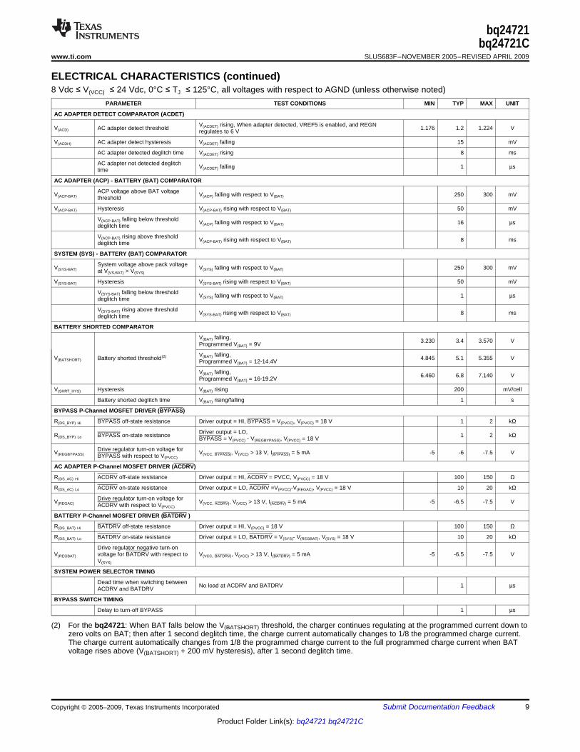
ELECTRICAL CHARACTERISTICS (continued)8 Vdc ≤ V(VCC) ≤ 24 Vdc, 0°C ≤ TJ ≤ 125°C, all voltages with respect to AGND (unless otherwise noted)
PARAMETER TEST CONDITIONS MIN TYP MAX UNIT
AC ADAPTER DETECT COMPARATOR (ACDET)
V(ACDET) rising, When adapter detected, VREF5 is enabled, and REGNV(ACD) AC adapter detect threshold 1.176 1.2 1.224 Vregulates to 6 V
V(ACDH) AC adapter detect hysteresis V(ACDET) falling 15 mV
AC adapter detected deglitch time V(ACDET) rising 8 ms
AC adapter not detected deglitch V(ACDET) falling 1 µstime
AC ADAPTER (ACP) - BATTERY (BAT) COMPARATOR
ACP voltage above BAT voltageV(ACP-BAT) V(ACP) falling with respect to V(BAT) 250 300 mVthreshold
V(ACP-BAT) Hysteresis V(ACP-BAT) rising with respect to V(BAT) 50 mV
V(ACP-BAT) falling below threshold V(ACP) falling with respect to V(BAT) 16 µsdeglitch time
V(ACP-BAT) rising above threshold V(ACP-BAT) rising with respect to V(BAT) 8 msdeglitch time
SYSTEM (SYS) - BATTERY (BAT) COMPARATOR
System voltage above pack voltageV(SYS-BAT) V(SYS) falling with respect to V(BAT) 250 300 mVat V(VS,BAT) > V(SYS)
V(SYS-BAT) Hysteresis V(SYS-BAT) rising with respect to V(BAT) 50 mV
V(SYS-BAT) falling below threshold V(SYS) falling with respect to V(BAT) 1 µsdeglitch time
V(SYS-BAT) rising above threshold V(SYS-BAT) rising with respect to V(BAT) 8 msdeglitch time
BATTERY SHORTED COMPARATOR
V(BAT) falling, 3.230 3.4 3.570 VProgrammed V(BAT) = 9V
V(BAT) falling,V(BATSHORT) Battery shorted threshold (2) 4.845 5.1 5.355 VProgrammed V(BAT) = 12-14.4V
V(BAT) falling, 6.460 6.8 7.140 VProgrammed V(BAT) = 16-19.2V
V(SHRT_HYS) Hysteresis V(BAT) rising 200 mV/cell
Battery shorted deglitch time V(BAT) rising/falling 1 s
BYPASS P-Channel MOSFET DRIVER (BYPASS)
R(DS_BYP) Hi BYPASS off-state resistance Driver output = HI, BYPASS = V(PVCC), V(PVCC) = 18 V 1 2 kΩ
Driver output = LO,R(DS_BYP) Lo BYPASS on-state resistance 1 2 kΩBYPASS = V(PVCC) - V(REGBYPASS), V(PVCC) = 18 V
Drive regulator turn-on voltage forV(REGBYPASS) V(VCC, BYPASS), V(VCC) > 13 V, I(BYPASS) = 5 mA -5 -6 -7.5 VBYPASS with respect to V(PVCC)
AC ADAPTER P-Channel MOSFET DRIVER (ACDRV)
R(DS_AC) Hi ACDRV off-state resistance Driver output = HI, ACDRV = PVCC, V(PVCC) = 18 V 100 150 Ω
R(DS_AC) Lo ACDRV on-state resistance Driver output = LO, ACDRV =V(PVCC)-V(REGAC), V(PVCC) = 18 V 10 20 kΩ
Drive regulator turn-on voltage forV(REGAC) V(VCC, ACDRV), V(VCC) > 13 V, I(ACDRV) = 5 mA -5 -6.5 -7.5 VACDRV with respect to V(PVCC)
BATTERY P-Channel MOSFET DRIVER (BATDRV )
R(DS_BAT) Hi BATDRV off-state resistance Driver output = HI, V(PVCC) = 18 V 100 150 Ω
R(DS_BAT) Lo BATDRV on-state resistance Driver output = LO, BATDRV = V(SYS)- V(REGBAT), V(SYS) = 18 V 10 20 kΩ
Drive regulator negative turn-onV(REGBAT) voltage for BATDRV with respect to V(VCC, BATDRV), V(VCC) > 13 V, I(BATDRV) = 5 mA -5 -6.5 -7.5 V
V(SYS)
SYSTEM POWER SELECTOR TIMING
Dead time when switching between No load at ACDRV and BATDRV 1 µsACDRV and BATDRV
BYPASS SWITCH TIMING
Delay to turn-off BYPASS 1 µs
(2) For the bq24721: When BAT falls below the V(BATSHORT) threshold, the charger continues regulating at the programmed current down tozero volts on BAT; then after 1 second deglitch time, the charge current automatically changes to 1/8 the programmed charge current.The charge current automatically changes from 1/8 the programmed charge current to the full programmed charge current when BATvoltage rises above (V(BATSHORT) + 200 mV hysteresis), after 1 second deglitch time.
Copyright © 2005–2009, Texas Instruments Incorporated Submit Documentation Feedback 9
Product Folder Link(s): bq24721 bq24721C

bq24721bq24721CSLUS683F–NOVEMBER 2005–REVISED APRIL 2009.................................................................................................................................................. www.ti.com
ELECTRICAL CHARACTERISTICS (continued)8 Vdc ≤ V(VCC) ≤ 24 Vdc, 0°C ≤ TJ ≤ 125°C, all voltages with respect to AGND (unless otherwise noted)
PARAMETER TEST CONDITIONS MIN TYP MAX UNIT
PWM HIGH-SIDE N-Channel MOSFET DRIVER (HIDRV), bq24721
R(DS_HIDRV) Hi High-side on-state resistance HSD switch on, HIDRV = HI, V(BOOST,PH) = 5.5 V 2.2 3 Ω
R(DS_HIDRV) Lo High-side off-state resistance HSD switch off, HIDRV = LO, V(BOOST,PH) = 5.5 V 1.5 2.5 Ω
PWM HIGH-SIDE N-Channel MOSFET DRIVER (HIDRV), bq24721C
R(DS_HIDRV) Hi High-side on-state resistance HSD switch on, HIDRV = HI, V(BOOST,PH) = 5.5 V 4.5 8.6 Ω
R(DS_HIDRV) Lo High-side off-state resistance HSD switch off, HIDRV = LO, V(BOOST,PH) = 5.5 V 1.5 2.6 Ω
PWM LOW-SIDE N-Channel MOSFET DRIVER (LODRV), bq24721
R(DS_LODRV) Hi Low-side on-state resistance LSD switch on, LODRV = HI, V(PVCC) = 7 V 2.2 3 Ω
R(DS_LODRV) Lo Low-side off-state resistance LSD switch off, LODRV = LO, V(PVCC) = 7 V 1.5 2.5 Ω
PWM LOW-SIDE N-Channel MOSFET DRIVER (LODRV), bq24721C
R(DS_LODRV) Hi Low-side on-state resistance LSD switch on, LODRV = HI, V(PVCC) = 7 V 4.5 8.6 Ω
R(DS_LODRV) Lo Low-side off-state resistance LSD switch off, LODRV = LO, V(PVCC) = 7 V 1.5 2.6 Ω
PWM LOW-SIDE DRIVER REGULATOR (REGN)
V(REGN) at I(REGN) = 10 mA, sourcing, 5.5 6 6.5 VAdapter detected (V(ACDET) > V(ACD)), V(PVCC) > 7 VVO(HREGN) REGN output voltage
V(REGN) at I(REGN) = 10 mA, sourcing, 4.2 VAdapter not detected, (V(ACDET) < V(ACD)), V(PVCC) > 7 V
2 times 25 nC load, fs = 300 kHz 15 mAREGN output current while chargerIO(REGN_SW) switching 2 times 25 nC load, fs = 500 kHz 25 mA
VREGN = 5 V 100 mAAdapter detected (V(ACDET) > V(ACD)), V(PVCC)> 7 VREGN Current limitI(REGN_LIM) Adapter detected VREGN = 0 V, shorted 13.3 mAAdapter detected (V(ACDET) > V(ACD)), V(PVCC)> 7 V
REGN Current limit VREGN = 4.2 V 15 mAAdapter not detected Adapter not detected, (V(ACDET) < V(ACD)), V(PVCC)> 7 V
PWM DRIVERS TIMING
Dead time when switching betweenLSD and HSD, no load at LSD and 30 nsHSD
PWM OSCILLATOR
PWM oscillator ramp voltage , lowV(RAMPLO) 0% duty cycle occurs below this threshold 0.35 Vvalue
PWM oscillator ramp voltage , highV(RAMPHI) near 100% duty cycle occurs above this threshold 3 Vvalue
VPP(RAMP) PWM ramp peak-to-peak amplitude 0.1×VCC V
V(RAMPCL) PWM oscillator ramp clamp voltage 3.5 V
FS PWM oscillator frequency (300 kHz) 265 300 345 kHz
PWM oscillator frequency (500 kHz) 425 500 575 kHz
INTERNAL SOFT START (8 steps to Ireg)
SRSET pin voltage number of steps Eight steps of charge current regulation to get to programmed value 8 stepduring soft start. (SRSET = 1 V).
Eight steps of charge current regulation to get to programmed valueStep Duration. 0.8 1 1.2 ms/step(SRSET = 1 V).
CHARGER SECTION POWER-UP SEQUENCING
Time delay between power up ofcharger block references (first) and 1 msstart charge (second)
Time delay from adapter detecteduntil ACDRV enable and charger 500 msblock enable
10 Submit Documentation Feedback Copyright © 2005–2009, Texas Instruments Incorporated
Product Folder Link(s): bq24721 bq24721C

TYPICAL CHARACTERISTICS
4.92
4.93
4.94
4.95
4.96
4.97
4.98
4.99
5
0 5 10 15 20 25 30 35 40 45 50
I − Load CurrentL − mA
VR
EF
5 L
oad
Reg
ula
tio
n -
V
T = 125 CJo
T = 85 CJo
T = 25 CJo
T =J 0 Co
V = 20 VI
4.974
4.976
4.978
4.98
4.982
4.984
4.986
4.988
7 9 11 13 15 17 19 21 23 24
V − Input VoltageI − V
VR
EF
5 L
ine
Re
gu
lati
on
- V
T = 125 CJo
T = 85 CJo
T = 25 CJo
T =J 0 Co
V = 20 VI
108
109
110
111
112
113
114
0 20 40 60 80 100 110 120 125
T − Junction TemperatureJ − Co
I-
VR
EF
5 C
urr
en
t L
imit
- m
AL
V = 20 VI
5.7
5.75
5.8
5.85
5.9
5.95
0 5 10 15 20 25 30 35 40 45 50
I − Load CurrentL − mA
RE
GN
Lo
ad
Reg
ula
tio
n -
V
T = 125 CJo
T = 85 CJo
T = 25 CJo
T =J 0 Co
V = 20 VI
5.87
5.88
5.89
5.9
5.91
5.92
7 9 11 13 15 17 19 21 23 24
V − Input VoltageI − V
RE
GN
Lo
in R
eg
ula
tio
n -
V
T = 125 CJo
T = 85 CJo
T = 25 CJo
T =J 0 Co
V = 20 VI
113
113.5
114
114.5
115
115.5
116
0 20 40 60 80 100 110 120 125
T − Junction TemperatureJ − Co
I-
RE
GN
Cu
rren
t L
imit
- m
AL
V = 20 VI
0
20
40
60
80
100
120
140
160
0 1 2 3 4 5 6
V − Forced REGN VoltageI − V
I-
RE
GN
Cu
rre
nt
Lim
it -
mA
L
V = 24 VCC
200
210
230
220
240
250
270
260
280
0 20 40 60 80 100 110 120 125
T − Junction TemperatureJ − Co
Qu
iescen
t C
urr
en
t, N
oA
dap
ter
-A
m
V = 12.6 VI
V = 16.8 VI
4
4.2
4.4
4.6
4.8
5
5.2
5.4
5.6
5.8
-15 5 25 45 65 85 105 125
T − Junction TemperatureJ − Co
Qu
escen
t C
urr
en
t,A
dap
ter
Co
nn
ecte
d -
mA
V = 12.6 VI
V = 16.8 VI
bq24721bq24721C
www.ti.com.................................................................................................................................................. SLUS683F–NOVEMBER 2005–REVISED APRIL 2009
VREF5 LOAD REGULATION VREF5 LINE REGULATION VREF5 CURRENT LIMITvs vs vs
LOAD CURRENT INPUT VOLTAGE JUNCTION TEMPERATURE
Figure 1. Figure 2. Figure 3.
REGN LOAD REGULATION REGN LINE REGULATION REGN CURRENT LIMITvs vs vs
LOAD CURRENT INPUT VOLTAGE JUNCTION TEMPERATURE
Figure 4. Figure 5. Figure 6.
QUIESCENT CURRENT, WITHREGN CURRENT LIMIT QUIESCENT CURRENT, NO ADAPTER ADAPTER
vs vs vsFORCED REGN VOLTAGE JUNCTION TEMPERATURE JUNCTION TEMPERATURE
Figure 7. Figure 8. Figure 9.
Copyright © 2005–2009, Texas Instruments Incorporated Submit Documentation Feedback 11
Product Folder Link(s): bq24721 bq24721C
1.1996
1.1998
1.2002
1.2
1.2004
1.2006
1.201
1.2008
1.2012
0 20 40 60 80 100 110 120 125
T − Junction TemperatureJ − Co
V-
AC
DE
T T
hre
sh
old
- V
I
V = 20 VI
18.75
18.9
18.85
18.8
19
18.95
19.05
19.1
19.2
19.15
19.25
0 20 40 60 80 100 110 120 125
T − Junction TemperatureJ − Co
V-
AC
DE
T H
ys
tere
sis
- m
Vh
ys
V = 20 VI
0 20 40 60 80 100 120 125
T − Junction TemperatureJ − Co
r-
HID
RV
Pu
ll U
p -
DS
(on
)W
V = 20 VI
1.5
2
2.5
3
3.5
4
4.5
5
5.5
6
bq24721C
bq24721
1
1.1
1.2
1.3
1.4
1.5
1.6
1.7
1.8
1.9
0 20 40 60 80 100 110 120 125
T − Junction TemperatureJ − Co
r-
HID
RV
Pu
ll D
ow
n -
DS
(on
)W
V = 20 VI
0 20 40 60 80 100 120 125
T − Junction TemperatureJ − Co
r-
LO
DR
V P
ull U
p -
DS
(on
)W
V = 20 VI
1.5
2
2.5
3
3.5
4
4.5
5
5.5
6
bq24721C
bq24721
1
1.1
1.2
1.3
1.4
1.5
1.6
1.7
1.8
1.9
0 20 40 60 80 100 110 120 125
T − Junction TemperatureJ − Co
r-
LO
DR
V P
ull
Do
wn
-D
S(o
n)
W
V = 20 VI
-0.1
-0.04
-0.06
-0.08
0
-0.02
0.02
0.04
0.08
0.06
0.1
Batt
ery
Vo
ltag
e R
eg
ula
tio
nA
ccu
racy -
%
0 20 40 60 80 100 110 120 125
T − Junction TemperatureJ − Co
V = 12.6 VI
V = 16.8 VI
-1
1
3
5
7
9
11
13
15
5 15 25 35 45 55 65
V − SPR-SRN VoltageI − mV
Ch
arg
e C
urr
en
t, R
eg
ula
tio
nA
cc
ura
cy
- %
V = 20 VI
T = 125 CJo
T = 85 CJo
T = 25 CJo
T =J 0 Co
-0.1
-0.04
-0.06
-0.08
0
-0.02
0.02
0.04
0.08
0.06
0.1
9 11 13 15 17 19
V − Battery Voltage(BAT) − V
Ba
tte
ry V
olt
ag
e R
eg
ula
tio
nA
cc
ura
cy
- % V = 24 VI
T = 125 CJo
T = 85 CJo
T = 25 CJo
T =J 0 Co
bq24721bq24721CSLUS683F–NOVEMBER 2005–REVISED APRIL 2009.................................................................................................................................................. www.ti.com
TYPICAL CHARACTERISTICS (continued)
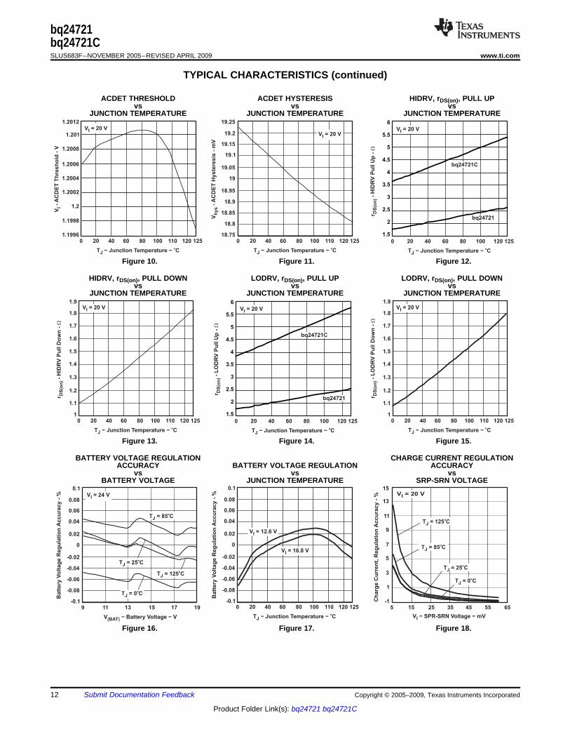
ACDET THRESHOLD ACDET HYSTERESIS HIDRV, rDS(on), PULL UPvs vs vs
JUNCTION TEMPERATURE JUNCTION TEMPERATURE JUNCTION TEMPERATURE
Figure 10. Figure 11. Figure 12.
HIDRV, rDS(on), PULL DOWN LODRV, rDS(on), PULL UP LODRV, rDS(on), PULL DOWNvs vs vs
JUNCTION TEMPERATURE JUNCTION TEMPERATURE JUNCTION TEMPERATURE
Figure 13. Figure 14. Figure 15.
BATTERY VOLTAGE REGULATION CHARGE CURRENT REGULATIONACCURACY BATTERY VOLTAGE REGULATION ACCURACY
vs vs vsBATTERY VOLTAGE JUNCTION TEMPERATURE SRP-SRN VOLTAGE
Figure 16. Figure 17. Figure 18.
12 Submit Documentation Feedback Copyright © 2005–2009, Texas Instruments Incorporated
Product Folder Link(s): bq24721 bq24721C
-1
1
3
5
7
9
11
13
5 9 13 17 21 25 29 3733 41
V − ACP-ACN VoltageI − mV
Inp
ut
Cu
rre
nt
Re
gu
lati
on
(D
PM
)A
cc
ura
cy
- %
V = 20 VI
T = 125 CJo
T = 85 CJo
T = 25 CJo
T =J 0 Co
-1
0
1
2
3
4
5
14 16 18 20 22 24
V − VoltageI − mV
Inp
ut
Cu
rre
nt
Re
gu
lati
on
(D
PM
)A
cc
ura
cy
- %
5.12 mV
10.24 mV
20.48 mV
V = 20 VI
40.96 mV
0.26
0.24
0.22
0.2
0.18
0.16
0.14
0.12
0.1
0.28
0 20 3010 40 50 60 70 80 90 100
V − ACP-ACN VoltageI − mV
I=
DP
M C
urr
en
t S
en
se
Am
pli
fie
rA
cc
ura
cy
- %
O
T = 125 CJo
T = 85 CJo
T = 25 CJo
T =J 0 Co
V = 20 VI
0.9
0.8
0.7
0.6
0.5
0.4
0.3
0.2
0.1
0
1
I=
DP
M C
urr
en
t S
en
se
Am
pli
fie
r O
ffs
et
- m
VO 20 40 60 80 100 110 120 125
T − Junction TemperatureJ − Co
V = 20 VI
5.6
5.65
5.75
5.7
5.8
5.85
5.95
5.9
6
0 20 40 60 80 100 110 120 125
T − Junction TemperatureJ − Co
IA
da
pte
r O
utp
ut
Cu
rre
nt
Lim
it -
mA
O-
0
-0.2
-0.4
-0.6
-0.8
-1
-1.2
-1.4
0.2
I=
Ch
arg
e C
urr
en
t S
en
se
Am
plifi
er
Accu
racy -
%O
0 20 3010 40 50 60 70 80 90 100
V − SRP-SRN VoltageI − mV
T = 125 CJo
T = 85 CJo
T = 25 CJo
T =J 0 Co V = 20 VI
5.4
5.45
5.5
5.55
5.6
5.65
5.7
5.75
0 20 40 60 80 100 110 120 125
T − Junction TemperatureJ − Co
I-
Ch
arg
e O
utp
ut
Cu
rre
nt
Lim
it -
mA
O
V = 20 VI
308
308.5
309
309.5
310
310.5
311
14 16 18 20 22 24
V − Input VoltageI − V
30
0-k
Hz S
wit
ch
ing
Fre
qu
en
cy
- k
Hz
T = 125 CJo
T = 85 CJo
T = 25 CJo
T =J 0 Co
308.5
309
309.5
310
310.5
311
300-k
Hz S
wit
ch
ing
Fre
qu
en
cy -
kH
z
0 20 40 60 80 100 110 120 125
T − Junction TemperatureJ − Co
V = 20 VI
bq24721bq24721C
www.ti.com.................................................................................................................................................. SLUS683F–NOVEMBER 2005–REVISED APRIL 2009
TYPICAL CHARACTERISTICS (continued)
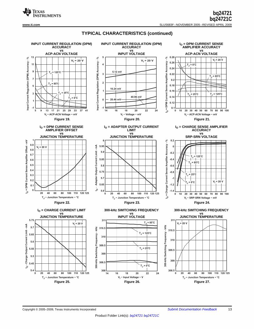
INPUT CURRENT REGULATION (DPM) INPUT CURRENT REGULATION (DPM) IO = DPM CURRENT SENSEACCURACY ACCURACY AMPLIFIER ACCURACY
vs vs vsACP-ACN VOLTAGE INPUT VOLTAGE ACP-ACN VOLTAGE
Figure 19. Figure 20. Figure 21.
IO = DPM CURRENT SENSE IO = ADAPTER OUTPUT CURRENT IO = CHARGE SENSE AMPLIFIERAMPLIFIER OFFSET LIMIT ACCURACY
vs vs vsJUNCTION TEMPERATURE JUNCTION TEMPERATURE SRP-SRN VOLTAGE
Figure 22. Figure 23. Figure 24.
IO = CHARGE CURRENT LIMIT 300-kHz SWITCHING FREQUENCY 300-kHz SWITCHING FREQUENCYvs vs vs
JUNCTION TEMPERATURE INPUT VOLTAGE JUNCTION TEMPERATURE
Figure 25. Figure 26. Figure 27.
Copyright © 2005–2009, Texas Instruments Incorporated Submit Documentation Feedback 13
Product Folder Link(s): bq24721 bq24721C

494.5
495
496
495.5
496.5
497
498
497.5
498.5
14 16 18 20 22 24
V − Input VoltageI − V
50
0-k
Hz S
wit
ch
ing
Fre
qu
en
cy
- k
Hz
T = 125 CJo
T = 85 CJo
T = 25 CJo
T =J 0 Co
0 20 40 60 80 100 110 120 125
T − Junction TemperatureJ − Co
V = 20 VI
494.5
495
496
495.5
496.5
497
498
497.5
498.5
500-k
Hz S
wit
ch
ing
Fre
qu
en
cy -
kH
z
0 20 40 60 80 100 110 120 125
T − Junction TemperatureJ − Co
V = 20 VI
73.35
73.4
73.45
73.5
73.6
73.55
73.65
VR
EF
% -
Th
erm
iste
r LT
F T
hre
sh
old
- %
0 20 40 60 80 100 110 120 125
T − Junction TemperatureJ − Co
V = 20 VI
34.35
34.36
34.365
34.355
34.375
34.37
34.395
34.39
34.385
34.38
34.4
VR
EF
% -
Th
erm
iste
r H
TF
Th
resh
old
- %
0 20 40 60 80 100 110 120 125
T − Junction TemperatureJ − Co
V = 20 VI
29.2
29.22
29.24
29.28
29.26
29.3
VR
EF
% -
Th
erm
iste
r T
CO
Th
resh
old
- %
0 20 40 60 80 100 110 120 125
T − Junction TemperatureJ − Co
V = 20 VI
84.7
84.72
84.71
84.74
84.73
84.78
84.77
84.76
84.75
84.8
84.79
VR
EF
% -
Th
erm
iste
r T
SD
ET
Th
resh
old
- %
bq24721bq24721CSLUS683F–NOVEMBER 2005–REVISED APRIL 2009.................................................................................................................................................. www.ti.com
TYPICAL CHARACTERISTICS (continued)
500-kHz SWITCHING FREQUENCY 500-kHz SWITCHING FREQUENCY THERMISTOR LTF THRESHOLDvs vs vs
INPUT VOLTAGE JUNCTION TEMPERATURE JUNCTION TEMPERATURE
Figure 28. Figure 29. Figure 30.
THERMISTOR LTF THRESHOLD THERMISTOR TCO THRESHOLD THERMISTOR TSDET THRESHOLDvs vs vs
JUNCTION TEMPERATURE JUNCTION TEMPERATURE JUNCTION TEMPERATURE
Figure 31. Figure 32. Figure 33.
14 Submit Documentation Feedback Copyright © 2005–2009, Texas Instruments Incorporated
Product Folder Link(s): bq24721 bq24721C
75
80
85
90
95
100
0 1 2 3 4 5 76 8
Battery Charge Current − A
Eff
icie
ncy -
%
V = 19.5 V
T = 20 CI
Ao
V = 12.6 V(BAT)
V = 16.8 V(BAT)
0
500
1000
1500
2000
2500
3000
3500
4000
4500
0 500 1 k 1.5 k 2 k 2.5 k 3.5 k3 k 4.5 k4 k
System Current − mA
Re
gu
lati
on
Cu
rre
nt
mA
−
V = 12 V
V = 20 V
R = 10 m
(BAT)
CC
(sns) W
ICHG
IDPM
DPM Active
ILOOP Active
BYPASS
ACDRV
BATDRV
t Time =− 100 ms/div
Ch
45 V
/div
Ch
12 V
/div
Ch
25 V
/div
Ch
35 V
/div
Ch120 V
Ch220 V
Ch10 V
Ch420 V
Adapter plugged in (ACDET goes above 1.2 V)ACDRV has a 500-ms delay before turning on
ACDET
Power Loop Verification (DPM) Transient Response
Constant Current Regulation, Then (DPM) Regulation
Ch4 = System Current
Ch1 = Input Current
Ch3 = Battery Current
t Time =− 1 ms/div
Ch
12
A/d
iv
Ch
32
A/d
ivC
h4
2A
/div
Ch1Ch30 A
Ch40 A
bq24721bq24721C
www.ti.com.................................................................................................................................................. SLUS683F–NOVEMBER 2005–REVISED APRIL 2009
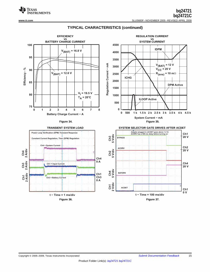
TYPICAL CHARACTERISTICS (continued)
EFFICIENCY REGULATION CURRENTvs vs
BATTERY CHARGE CURRENT SYSTEM CURRENT
Figure 34. Figure 35.
TRANSIENT SYSTEM LOAD SYSTEM SELECTOR GATE DRIVES AFTER ACDET
Figure 36. Figure 37.
Copyright © 2005–2009, Texas Instruments Incorporated Submit Documentation Feedback 15
Product Folder Link(s): bq24721 bq24721C
System Power Selection
Adapter is plugged in, then 500 ms later the system switches over.
1-A System Load
Battery Voltage
Adapter Voltage
System Voltage
t Time =− 200 ms/div
Ch
45
V/d
ivC
h1
5 V
/div
Ch
25
V/d
iv
Ch1Ch2Ch40 V
System Power Selection
Adapter is unplugged in, System switches over to battery once the adaptervoltage drops below VAIRLINE.
1-A System Load
Battery Voltage
Adapter Voltage
System Voltage
t Time =− 1 s/div
Ch
45
V/d
ivC
h1
5 V
/div
Ch
25
V/d
iv
Ch1Ch2Ch40 V
Softstart Operation
t Time =− 1 ms/div
Ch
31
A/d
iv
Inductor Current
0 A
REGN
VREF5
AVCC/PVCC
VREF5 and REGN Power-Up
t Time =− 2 ms/div
Ch
15 V
/div
Ch
42 V
/div
Ch
22 V
/div
Ch40 V
Ch10 V
Ch20 V
bq24721bq24721CSLUS683F–NOVEMBER 2005–REVISED APRIL 2009.................................................................................................................................................. www.ti.com
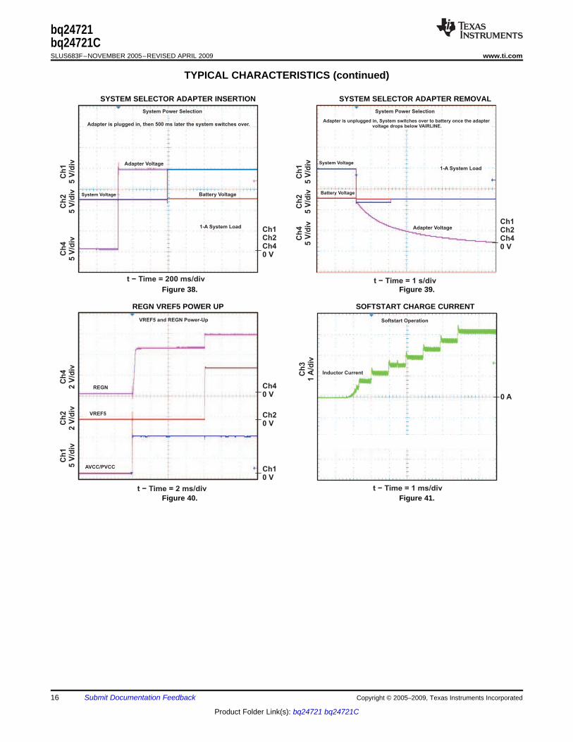
TYPICAL CHARACTERISTICS (continued)
SYSTEM SELECTOR ADAPTER INSERTION SYSTEM SELECTOR ADAPTER REMOVAL
Figure 38. Figure 39.
REGN VREF5 POWER UP SOFTSTART CHARGE CURRENT
Figure 40. Figure 41.
16 Submit Documentation Feedback Copyright © 2005–2009, Texas Instruments Incorporated
Product Folder Link(s): bq24721 bq24721C
PH
t Time =− 10 s/divm
Ch
110 V
/div
Ch
45 V
/div
Ch
31
A/d
iv
Transition from Non-Synchronous to Synchronous
Low side NMOS gate voltage
Inductor Current
Ch30 A
Ch10 V
Ch40 V
PH
t Time =− 10 s/divm
Ch
110 V
/div
Ch
45 V
/div
Ch
31
A/d
iv
Transition from Non-Synchronous to Synchronous
Low side NMOS gate voltage
Inductor Current
Ch30 A
Ch10 V
Ch40 V
PH
t Time =− 40 s/divm
Ch
11
0 V
/div
Ch
25
V/d
ivC
h3
2A
/div
Low side NMOS gate
Inductor Current
Trefresh = 250 sm
Bootstrap Refresh Comparator Operation
Ch30 A
Ch10 V
Ch20 V
t Time =− 400 s/divm
Ch
25
V/d
ivC
h3
1A
/div
BAT goes from 13 V to 3 V, 1 sec deglitch, charge turns offBAT goes back to 13 V, 1 sec deglitch, charge turns back on
Inductor Current
BAT
BATSHORT Functionality
Ch20 V
Ch30 A
bq24721bq24721C
www.ti.com.................................................................................................................................................. SLUS683F–NOVEMBER 2005–REVISED APRIL 2009
TYPICAL CHARACTERISTICS (continued)
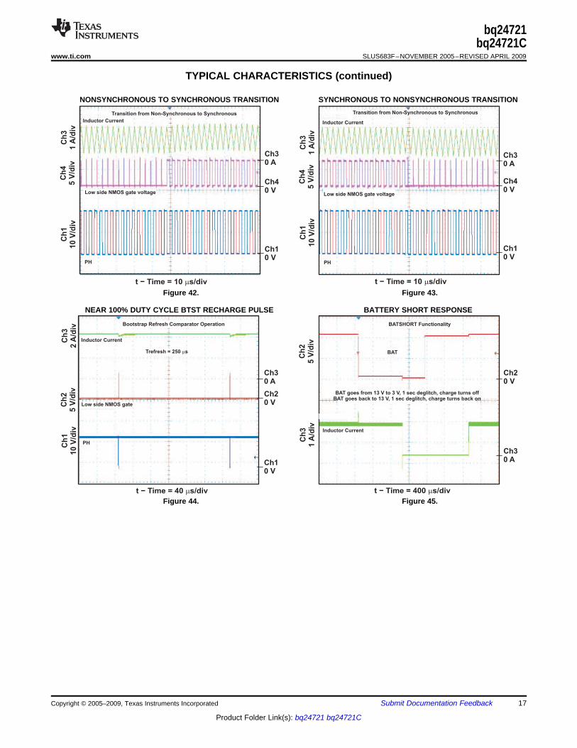
NONSYNCHRONOUS TO SYNCHRONOUS TRANSITION SYNCHRONOUS TO NONSYNCHRONOUS TRANSITION
Figure 42. Figure 43.
NEAR 100% DUTY CYCLE BTST RECHARGE PULSE BATTERY SHORT RESPONSE
Figure 44. Figure 45.
Copyright © 2005–2009, Texas Instruments Incorporated Submit Documentation Feedback 17
Product Folder Link(s): bq24721 bq24721C
VBAT
t Time =− 20 s/divm
Ch
22 V
/div
Ch
32
A/d
iv
Regulating 4 A, then add 1 in parallelto reduce VBAT
W
Inductor Current
Charge Overcurrent Comparator Functionality
Ch20 V
Ch34 A
ADCRV
t Time =− 20 s/divm
Ch
15 V
/div
Ch
22 V
/div
ACN decreases below ACOC threshold
ACN (ACP fixed)
ACOC Rising Edge (32 s deglitch)m
Ch120 V
Ch220 V
Ch2 = VPH
Ch1 = VOUTCAPS
Ch3 = Inductor Current
t Time =− 1 s/divm
Ch
21
0 V
/div
Ch
11
0 V
/div
Ch
45
0 m
V/d
ivC
h3
2A
/div
Max (C1) 10.4 VMax (C2) 20.4 VMax (C3) 5.04 AMax (C4) 42.0 mV
Min (C1) 8.0 VMin (C2) -1.2 VMin (C3) 3.12 AMin (C4) 32.0 mV
Ch4 = VOUTCAPS_AC Ripple
Steady State Operation
Ch112 V
Ch34 A
Ch20 V
Ch412 V
ADCRV
t Time =− 200 s/divm
Ch
15 V
/div
Ch
22 V
/div
ACN increases above ACOC threshold
ACN (ACP fixed)
ACOC Falling Edge (500 s deglitch)m
Ch120 V
Ch220 V
bq24721bq24721CSLUS683F–NOVEMBER 2005–REVISED APRIL 2009.................................................................................................................................................. www.ti.com
TYPICAL CHARACTERISTICS (continued)
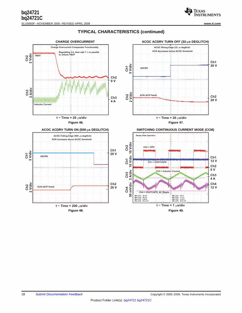
CHARGE OVERCURRENT ACOC ACDRV TURN OFF (32-µs DEGLITCH)
Figure 46. Figure 47.
ACOC ACDRV TURN ON (500-µs DEGLITCH) SWITCHING CONTINUOUS CURRENT MODE (CCM)
Figure 48. Figure 49.
18 Submit Documentation Feedback Copyright © 2005–2009, Texas Instruments Incorporated
Product Folder Link(s): bq24721 bq24721C
Ch2 = VPH
Ch1 = VOUTCAPS
Ch3 = InductorCurrent
t Time =− 1 s/divm
Ch
21
0 V
/div
Ch
11
0 V
/div
Ch
45
0 m
V/d
ivC
h3
2A
/div
Ch4 = VOUTCAPS_AC Ripple
Steady State Operation
Max (C1) 14.0 VMax (C2) 20.8 VMax (C3) 1.12 AMax (C4) 30.0 mV
Min (C1) 11.6 VMin (C2) -1.2 VMin (C3) 320.0 mAMin (C4) 22.0 mV
Ch112.6 V
Ch34 A
Ch20 V
Ch412.6 V
bq24721bq24721C
www.ti.com.................................................................................................................................................. SLUS683F–NOVEMBER 2005–REVISED APRIL 2009
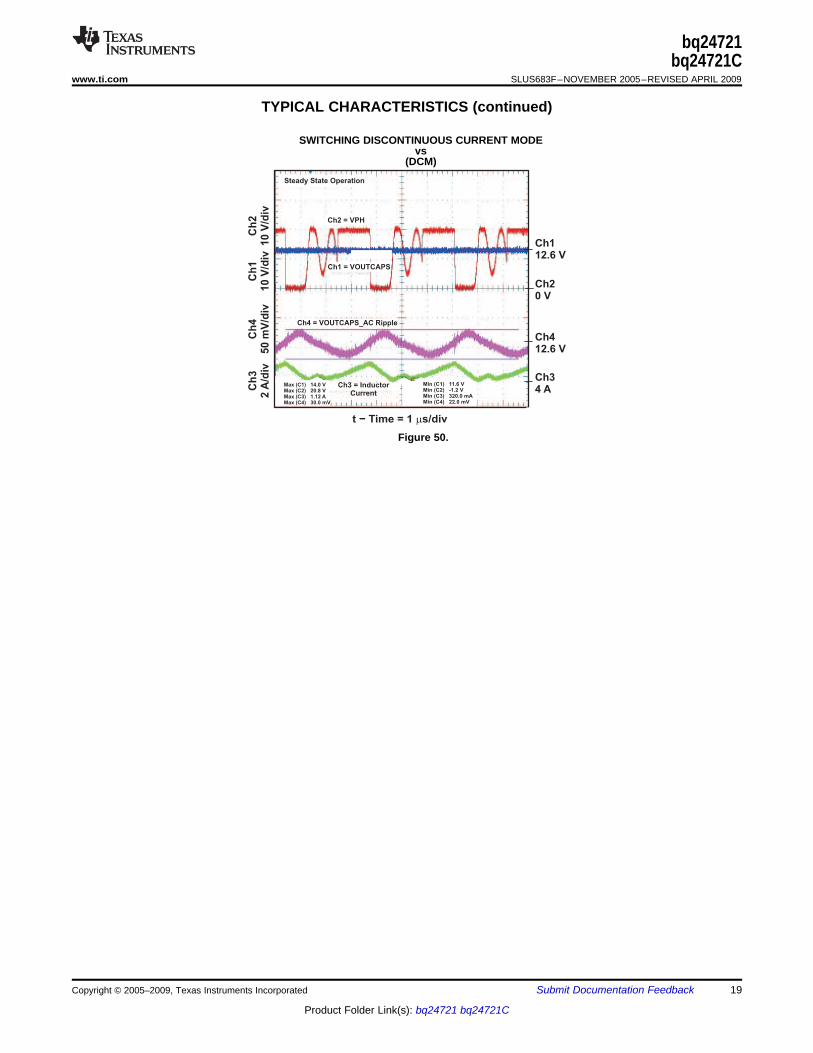
TYPICAL CHARACTERISTICS (continued)
SWITCHING DISCONTINUOUS CURRENT MODEvs
(DCM)
Figure 50.
Copyright © 2005–2009, Texas Instruments Incorporated Submit Documentation Feedback 19
Product Folder Link(s): bq24721 bq24721C
ACP
ACN
PH
REGN
LODRV
HIDRV
SRP
IOUT
EAO
SRN
VCC
ACDET
20X
Select Adaptor current
or Charge current
Always on
BAT
VREF5
TS
BTST
SYNCHRONOUS SWITCHINGPWM CONVERTER
− current loop
− dpm loop
− voltage loop
− sync/nonsync comparator
− charge overcurrent
− comparator
− charge current reference
− dpm current reference
− break−before−make logic
− duty−cycle limited, 0% to near
100% (99.5%)
− NMOS/NMOS drivers
− Internal soft start
− PWM oscillator 300 kHz/500 kHz
Enabled only when AC is
detected and is lowCHGEN
REFERENCE SYSTEM
− 5v ldo when ACPRES
− Power−on reset
− UVLO
− Voltage references
− Internal timebase
Always on
AGND
SYS
SYSTEM STATUS
COMPARATORS
− Battery depleted (1)
− AC detection (1)
− *Thermistor inserted (1)
− *Thermistor cold (2)
− *Thermistor hot (2)
− System voltage / pack voltage (2)
− VCC above pack voltage (2)
(1) always on
(2) enabled when AC is detected
LOGIC
− Power up/down sequencing
− Charge enable logic
− Charge enable sequencing
− System power selector logic
− System selector bbm logic
− Deglitch times
Always on
AC SW AND BAT SW DRIVERS
− break−before−make LOGIC
Always on
BYPASS SW
DRIVER
Always on
ACGOOD
BDEP, ACCHG, THDET,TCOLD, THOT ,VSHI, TERMDET,
ADPSRC, VCCGTBAT, TCMPCHARGERON
POWERON
ACONBYPON
CLK, POR
SYNP
CHGOC
ACOC
PGND
SMBUS INTERFACE
Always on
MEMORY
Always on
SR IREG DAC
7BIT (1.28mV/bit)
VREG DAC
DECODER
SBS [b1−b14] to
bq24721 [7bit +1bit]
SDA
SCL
ALARM
SYNN
ISYNSET
EAI
FBO
PVCC
AC IREG DAC
7BIT (1.28mV/bit)
TTL INPUT
BUFFER
CHGEN
VREG DAC
1BIT Select Cells
7BIT (6.25mV/bit)
BYPASS ACDRV BATDRV
bq24721bq24721CSLUS683F–NOVEMBER 2005–REVISED APRIL 2009.................................................................................................................................................. www.ti.com
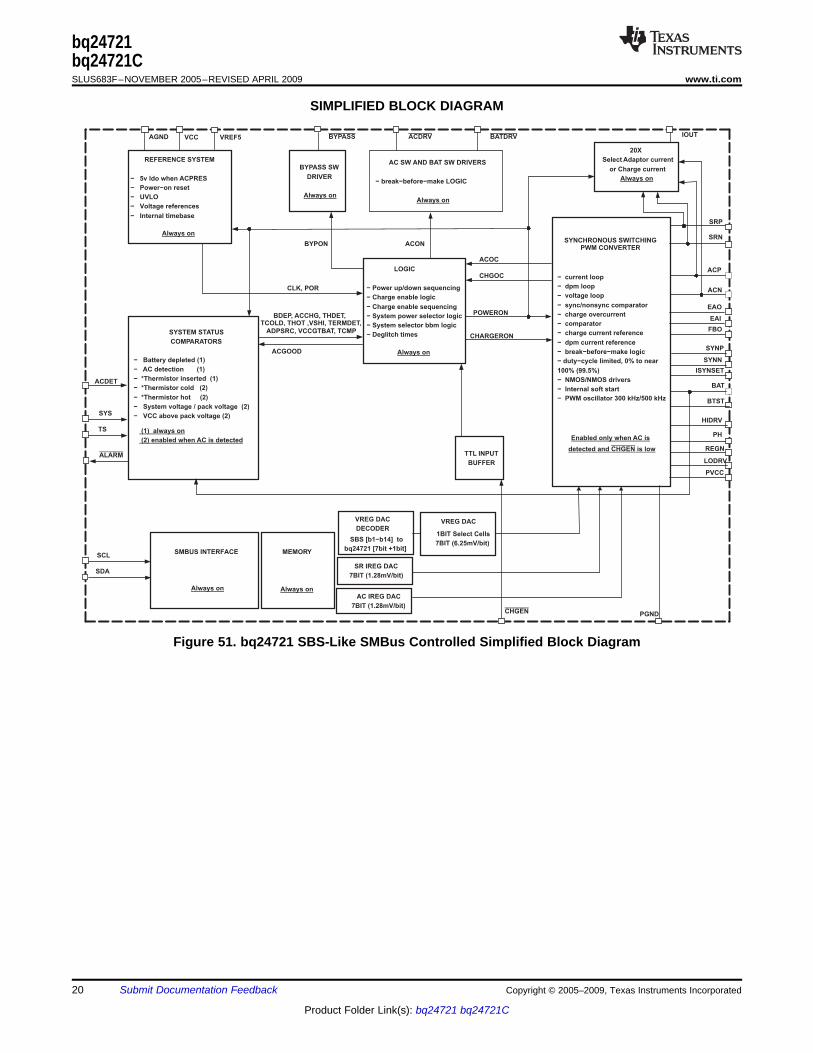
SIMPLIFIED BLOCK DIAGRAM
Figure 51. bq24721 SBS-Like SMBus Controlled Simplified Block Diagram
20 Submit Documentation Feedback Copyright © 2005–2009, Texas Instruments Incorporated
Product Folder Link(s): bq24721 bq24721C
TYPICAL APPLICATION bq24721
PACK+
ADAPTER+
SYSTEM
PACK-
PACK+
ADAPTER-
C8
0.1uF
D1BAT54C
R2
0.010
L110 uH
C3
4x10uF
C52x10 uF
C14
0.1uF
C210 uF
C11
0.1uF
C15
0.1uFC160.1 uF
C190.1 uF
C180.1 uFOPTIONAL
C170.1 uF
OPTIONAL
D2
BAT54
C12 , 0.1uF
C13, 1uF
R12
33k
R10
20k
R11
200k
R9
7.5k
C21
2000pF
C20
51pF C22
130pF
C9
0.1uF
bq24721
ACN
ACP
CHGEN
AGND
VCC
PVCC
BTST
PH
REGN
HIDRV
LODRV
SRP
SRN
BAT
BYPASS
ISYNSET
VREF5
TS
SCL
BATDRV
SYS
ACDRV
ACDET
SYNP
PGND
SDA
ALARM
IOUT
SYNN
EAO
EAI
FBO
PowerPAD
Short PowerPAD toPGND and AGND
VREF5
VREF5
R13118 k
1%
R433.2 k1%
R3464 k1%
R55.6 k
1%
EMBEDDEDCONTROLLER
HOST
A/D
SMBus
IRQ
R810 k
R710 k
R610 k
C110 uF
ACGOOD
PACKTHERMISTOR
SENSE
C101 uF
C61 uF
R10.010
Q1SI4435
Q2SI4435
Q5SI4435
C70.1 uF
Q3FDS6670A
Q4FDS6670A
C42x10 uF
bq24721bq24721C
www.ti.com.................................................................................................................................................. SLUS683F–NOVEMBER 2005–REVISED APRIL 2009
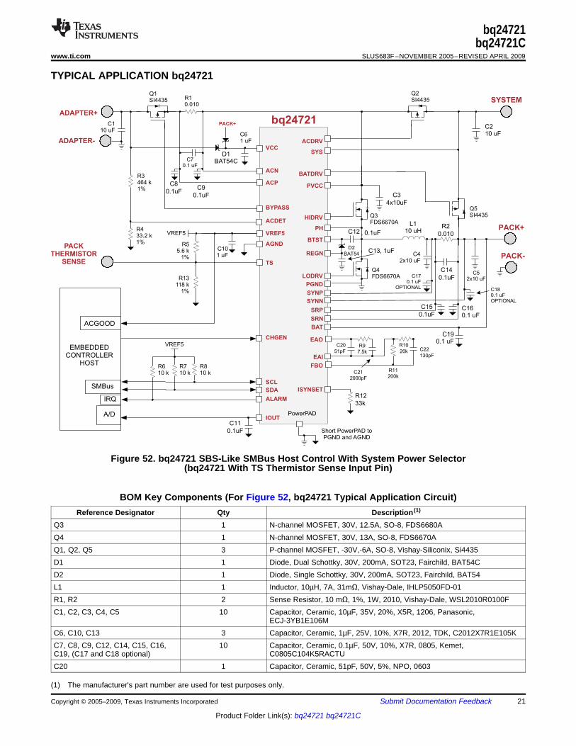
Figure 52. bq24721 SBS-Like SMBus Host Control With System Power Selector(bq24721 With TS Thermistor Sense Input Pin)
BOM Key Components (For Figure 52, bq24721 Typical Application Circuit)Reference Designator Qty Description (1)
Q3 1 N-channel MOSFET, 30V, 12.5A, SO-8, FDS6680AQ4 1 N-channel MOSFET, 30V, 13A, SO-8, FDS6670AQ1, Q2, Q5 3 P-channel MOSFET, -30V,-6A, SO-8, Vishay-Siliconix, Si4435D1 1 Diode, Dual Schottky, 30V, 200mA, SOT23, Fairchild, BAT54CD2 1 Diode, Single Schottky, 30V, 200mA, SOT23, Fairchild, BAT54L1 1 Inductor, 10µH, 7A, 31mΩ, Vishay-Dale, IHLP5050FD-01R1, R2 2 Sense Resistor, 10 mΩ, 1%, 1W, 2010, Vishay-Dale, WSL2010R0100FC1, C2, C3, C4, C5 10 Capacitor, Ceramic, 10µF, 35V, 20%, X5R, 1206, Panasonic,
ECJ-3YB1E106MC6, C10, C13 3 Capacitor, Ceramic, 1µF, 25V, 10%, X7R, 2012, TDK, C2012X7R1E105KC7, C8, C9, C12, C14, C15, C16, 10 Capacitor, Ceramic, 0.1µF, 50V, 10%, X7R, 0805, Kemet,C19, (C17 and C18 optional) C0805C104K5RACTUC20 1 Capacitor, Ceramic, 51pF, 50V, 5%, NPO, 0603
(1) The manufacturer's part number are used for test purposes only.
Copyright © 2005–2009, Texas Instruments Incorporated Submit Documentation Feedback 21
Product Folder Link(s): bq24721 bq24721C

Typical bq24721 Narrow VDC (NVDC) Application (2 sense resistors)
ACN
ACP
CHGEN
AGND
VCC
PVCC
BTST
PH
REGN
HIDRV
LODRV
SRP
SRN
BAT
BYPASS
ISYNSET
VREF5
TS
ADAPTER +bq24721
SCL
SYSTEM
BATDRV
SYS
ACDRV
ACDET
PACK+
SYNP
PGND
SDA
ALARM
IOUT
SYNN
ADAPTER -
EMBEDDED
CONTROLLER
HOST
A/D
SMBus
IRQ
EAO
EAI
FBO
VREF5
R55.6 k
1%
C10
1uF
C6
1uF
C8
0.1uF
C7
0.1uF
PowerPAD
Short PowerPAD toPGND and AGND
VREF5
R8
10k
R7
10k
R6
10k
D1BAT54C
R2
0.010L1
10uH
Q3FDS6670A
Q4FDS6670A
Q1SI4435
C1
10uF
C34x10uF
C4
2x10uF
C52x10uF
C14
0.1uF
C210 uF
R3
464k
1%
R4
33.2k
1%
C11
0.1uF
C19
0.1uF
C15
0.1uFC16
0.1uF
C18
0.1uF
C17
0.1uF
D2
BAT54
C12, 0.1uF
C13, 1uF
R12
33k
R10
20k
R11200 k
R9
7.5k
C212000 pF
C20
51pF C22130 pF
C9
0.1uF
ACGOOD
PACK+
PACK-
R13
0.010
PACK
THERMISTOR
SENSE
R1118k
1%
bq24721bq24721CSLUS683F–NOVEMBER 2005–REVISED APRIL 2009.................................................................................................................................................. www.ti.com
BOM Key Components (For Figure 52, bq24721 Typical Application Circuit) (continued)Reference Designator Qty Description (1)
C21 1 Capacitor, Ceramic, 2000pF, 50V, 5%, X7R, 0805C22 1 Capacitor, Ceramic, 130pF, 50V, 5%, NPO, 0603R3 1 Resistor, Chip, 464kΩ, 1/16W, 1%, 0402R4 1 Resistor, Chip, 33.2kΩ, 1/16W, 1%, 0402R12 1 Resistor, Chip, 33kΩ, 1/16W, 5%, 0402R9 1 Resistor, Chip, 7.54kΩ, 1/16W, 1%, 0402R10 1 Resistor, Chip, 20kΩ, 1/16W, 1%, 0402R11 1 Resistor, Chip, 200kΩ, 1/16W, 1%, 0402R6, R7, R8 3 Resistor, Chip, 10kΩ, 1/16W, 5%, 0402R5 1 Resistor, Chip, 5.6kΩ, 1/16W, 1%, 0402R13 1 Resistor, Chip, 118kΩ, 1/16W, 1%, 0402
Figure 53. bq24721 SBS-Like SMBus Host Control, NVDC (no system power selector) With 2 SenseResistors. ACP and ACN Regulating Converter Current Instead of Input Current
22 Submit Documentation Feedback Copyright © 2005–2009, Texas Instruments Incorporated
Product Folder Link(s): bq24721 bq24721C
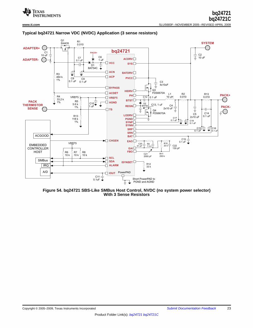
Typical bq24721 Narrow VDC (NVDC) Application (3 sense resistors)
ADAPTER+bq24721
SYSTEM
PACK+
ADAPTER-
EMBEDDEDCONTROLLER
HOST
A/D
SMBus
IRQ
C61 uF
C210 uF
0.1 uF
VREF5
VREF5
R810 k
R13118 k
1%
R433.2 k1%
R3464 k1%
R55.6 k
1%
R710 k
R610 k
D1BAT54C
R10.010
L110 uH
R20.010
R130.010
Q3FDS6670A
Q4FDS6670A
Q1SI4435
C34x10uF
C42x10 uF
C52x10 uF
C140.1 uF
C110.1uF
C101 uF
C110 uF
C70.1 uF
C90.1 uF
C80.1 uF
C180.1 uF
C170.1 uF
C150.1 uF
C190.1 uF
C22130 pF
C212000 pF
C160.1 uF
D2BAT54
C12
C13, 1 uF
R1020 k
R97.5 k
R11200 k
R1233 k
C2051 pF
ACGOOD
PACK+
PACK-
PACKTHERMISTOR
SENSE
ACN
ACP
CHGEN
AGND
VCC
PVCC
BTST
PH
REGN
HIDRV
LODRV
SRP
SRN
BAT
BYPASS
ISYNSET
VREF5
TS
SCL
BATDRV
SYS
ACDRV
ACDET
SYNP
PGND
SDA
ALARM
IOUT
SYNN
EAO
EAI
FBO
PowerPAD
Short PowerPAD toPGND and AGND
bq24721bq24721C
www.ti.com.................................................................................................................................................. SLUS683F–NOVEMBER 2005–REVISED APRIL 2009
Figure 54. bq24721 SBS-Like SMBus Host Control, NVDC (no system power selector)With 3 Sense Resistors
Copyright © 2005–2009, Texas Instruments Incorporated Submit Documentation Feedback 23
Product Folder Link(s): bq24721 bq24721C
IOUT
VREF5
PVCC
BYPASS
ACDRV
SYS
BATDRV
BTST
HIDRV
PH
REGN
LODRV
PGND
ALARM
SDA
SCL
ISYNSET
ISYNSET x 500
VCC
ACDET
CHGEN
EAO
EAI
FBO
ACP
ACN
BAT
SRP
SRN
SYNP
SYNN
TS
AGND
5-V LDO
6-V LDO
V(ACP-ACN)+
-
V(SRP-SRN)+
-
V(SYNP-N)+
-
ADAPTER
DETECTED+
-
COMP
ERROR
AMPLIFIER
+
-ACP-BAT
+
-
OCP
+
-
SYNCH+
-
+_
1 V
TSDET+
-
LTF
+
-
HTF
VREF5
V(IADAPT)+
-
V(IBAT)+
-20x
20xACP
ACN
SRP
SRN
1.2 V
ENA
+
-
+
- BAT_ER
ICH_ER
ICH_ER
+
-
1 V
20 Am
20 Am
BAT + 250 mV
250 mV
+ _
IINDAC
VBAT
DAC
IBAT
DAC
2 x IBAT_DAC
SYSSYS-6V
SYS-6V
PVCC-6V
PVCC-6V
PVCC-6V
PVCCPVCC-6V
LDO
SYS 6-VLDO
DC-DCCONVERTERPWM LOGIC
VCC
+
-
PH
4.5 V +_
BTST REFRESHCBTST
SYSTEMPOWER
SELECTORLOGIC
CHGEN
SMBUSCHGEN
OCP
SYNCH
ACP-BAT
ACOC
SRP-BAT
TCO+
-
+
-
+
-SMBUS
BATDEPSET
BAT
SUSPEND
BATDEP
SUSPEND
TSDET
SMBus LOGIC
IBATDAC
VBATDAC
IIN (DPM)DAC
CHARGE STATUSREGISTER
CHARGE MODEREGISTER
SELECT
ACOC+
-
ACOC_SET
145 Co
IC TJ TSHUT+
-
+
-
BAT + 250 mV
250 mV
+ _
SYS SYS-BAT
LEVELSHIFTER
SW FREQSELECT
300 kHz500 kHz
bq24721bq24721CSLUS683F–NOVEMBER 2005–REVISED APRIL 2009.................................................................................................................................................. www.ti.com
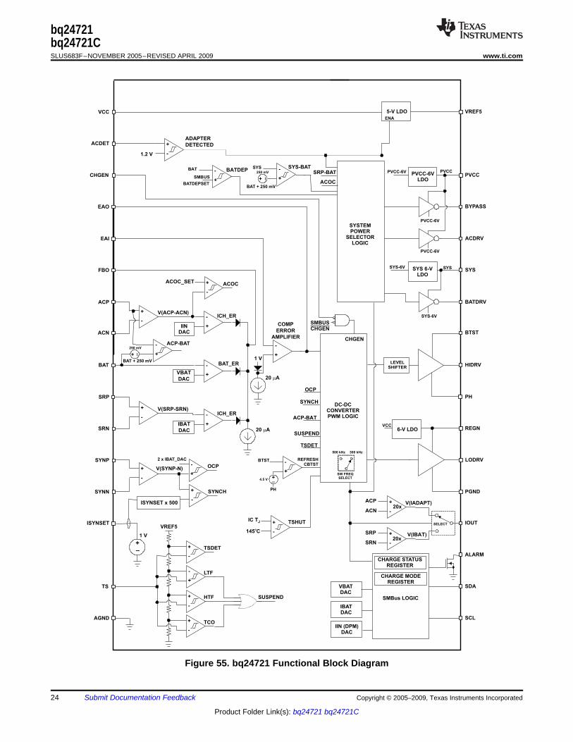
Figure 55. bq24721 Functional Block Diagram
24 Submit Documentation Feedback Copyright © 2005–2009, Texas Instruments Incorporated
Product Folder Link(s): bq24721 bq24721C

bq24721
BATTERY
CHARGER
CONTROLLER
IC
&
CONVERTER
SYSTEM & CHARGEPOWER
SELECTOR
ADAPTER
POWER
externalSYSTEM
HOST - Embedded Controller (EC)
Chrg DischrgChrg Dischrg
BatVin
SMBus SMBus SMBus I/OPSID I/O
BATTERY
PrimaryBATTERY
Secondary
BLOCK DESCRIPTION
Detail Block Diagram
SMBus Interface
bq24721bq24721C
www.ti.com.................................................................................................................................................. SLUS683F–NOVEMBER 2005–REVISED APRIL 2009
Figure 56. Host Controller
The bq24721 charge controller can be used to charge Li-Ion, NiMH, or NiCd batteries. The high efficiencysynchronous buck controller uses n-channel power MOSFETs for both the high-side control device and thelow-side synchronous device. The controller offers high regulation accuracy of the charge current, batteryvoltage, and input current limits. The low offset of the current loops allow using sense resistors with low-value,such as 10 mΩ.
An embedded controller host programs the battery voltage, charge current, and input current regulation limitthresholds through an SMBus interface using SBS-like DAC registers. The embedded host can control theoperation of the charger through a Charge Control (0x12) register, and monitor the status of the charger througha Charger Status (0x13) register.
The voltage loop regulates the battery voltage to the programmed value, and prevents the voltage fromexceeding that value when the battery is connected. The charge current loop regulates the battery charge currentto the programmed value, and prevents the charge current from exceeding that value. Through the use ofdynamic power management (DPM), the input current loop regulates the battery charge current to theprogrammed value, and prevents the input current from exceeding that value. The three regulation loops operateindependently, yet only require a single loop compensation network.
The system power selector function selects the appropriate power source for the system load. If the adapter isdetected, then the adapter is connected to the system load. When the adapter is removed, the battery is selectedto power the system load. A battery learn cycle is performed when the adapter is present by setting theCONTROL(0x12) register into Learn Mode via SMBus by the embedded host. This disconnects the adapter fromthe system; and instead, connect the battery to the system. This is typically done for Ni-based batteries.
The bq24721 uses all the SMBus communications protocol, except for packet error correction (PEC). Thecharger IC address is (0x12), although it is not 100% SBS compliant. In most applications, the extra functionalityprovided by the differing SBS-Like interface enhances the control of the charger application, while simplifying theinterface block, using only the pertinent functions. Five 16-bit registers are used to interface between theembedded host and the charge control IC. The Charging Voltage (0x15) register is used to set the batteryregulation voltage. The Charging Current (0x14) register is used to set the battery charge regulation current. TheInput Current (0x3F) register is used to set the input regulation current. The Charger Mode (0x12) control registeris used to set the charger operating modes. Finally, the Charger Status (0x13) register is used to monitor theoperating status of the charger.
Copyright © 2005–2009, Texas Instruments Incorporated Submit Documentation Feedback 25
Product Folder Link(s): bq24721 bq24721C

Setting Charge Voltage (VBAT DAC register)
Setting Charge Current (IBAT DAC register)
bq24721bq24721CSLUS683F–NOVEMBER 2005–REVISED APRIL 2009.................................................................................................................................................. www.ti.com
ADDRESS REGISTER DESCRIPTION0x15 Charging voltage Used to set the battery regulation voltage.0x14 Charging current Used to set the battery charge regulation current.0x3F Input current Used to set the input regulation current.0x12 Charger mode Used to set the charger operating modes.0x13 Charger status Used to monitor the operating status of the charger.
The SMBus communications requires only two pins besides the analog ground pin—through the SDA (data) andSCL (clock) pins. The open-drain SCL and SDA pins require pull-up resistors on the board pulling up to the hostdigital output voltage rail. The pins can be pulled up to any rail between 3 V to 5 V.
An alarm is sent to the host through the ALARM open drain pin. This is used to trigger an interrupt request (IRQ).A low on the ALARM pin indicates there was a change on the Charger Status (0x13) register. The ALARM pinstays low until the host reads the Charger Status (0x13) register, then the ALARM pin clears and returns to theHI state. The open-drain ALARM pin requires a pull-up resistor that pulls up to the host digital input voltage rail.The pin can be pulled up to any rail between 3 V to 5 V. The charge controller continues to operate whether thehost chooses to read or not to read the Charger Status (0x13) register. There is no communications watchdogtimer, so there is no need to continuously poll the Charger Status (0x13) register or have to continuouslyreprogram any of the other registers.
The charge voltage can be programmed by setting Charging Voltage(0x15) register. The SBS specification asksfor 16 bits to set the regulation voltage with a 1-mV LSB—giving a maximum possible voltage of 65.535 V. Thebq24721 uses bits 1 through 14 only, and maps them into the closest value of an internal 7-bit DAC on a per cellbasis using a 6.25-mV per cell LSB for three ranges: 9-V precharge voltage; 3 cells Li+ battery pack range; or 4cells Li+ battery pack range. The 3 cell portion has an LSB of 18.75 mV and a range from 12 V-14.4 V; while the4 cell portion has an LSB of 25 mV and a range from 16 V-19.2 V. Intermediate programmed voltages betweenthe internal 7-bit DAC values are truncated to the lower value to avoid an overvoltage on the battery.Programmed voltages above 19.2 V are automatically set to the maximum 19.2-V limit. The charger is disabledfor programmed voltages below 12 V (except for 9 V), and for programmed voltages between 14.4 V–16 V. Thistriggers a voltage-out-of-range condition and the VOR bit of the Charger Status (0x13) register is set, and analarm (ALARM pin pulled low) is sent to the host. The default power-up-reset voltage value is 0 V, chargerdisabled.
The charge current can be programmed using the Charging Current (0x14) register. The SBS specification asksfor 16 bits to set the charge current with a 1-mA LSB—giving a maximum possible current of 65.535 A using a10-mΩ sense resistor. The bq24721 uses bits 7 – 14 only to limit the range within a practical operating range.The current range is 0 mA to 16.384 A with an LSB of 128 mA using a 10-mΩ sense resistor. The charger isdisabled when the programmed input current is 0 A. The default power-up-reset current value is 0 A, chargerdisabled. Other sense resistors can be used to set the charge current—the user needs to transform the DACcurrent table values to the new current values by dividing the current by 10 mΩ, then multiplying by the newsense resistor value used.
26 Submit Documentation Feedback Copyright © 2005–2009, Texas Instruments Incorporated
Product Folder Link(s): bq24721 bq24721C

Setting Input (DPM) Current (IDPM DAC register)
Power Up
Adapter Detect
bq24721bq24721C
www.ti.com.................................................................................................................................................. SLUS683F–NOVEMBER 2005–REVISED APRIL 2009
The input current can be similarly programmed using the Input Current (0x3F) register. The SBS specificationasks for 16 bits to set the input current with a 1-mA LSB—giving a maximum possible current of 65.535 A usinga 10-mΩ sense resistor. The bq24721 uses bits 7 – 14 only to limit the range within a practical operating range.The current range is 0 mA to 16.384 A with an LSB of 128 mA using a 10-mΩ sense resistor. The charger isdisabled when the programmed input current is 0 A. The default power-up-reset current value is 0 A, chargerdisabled. Other sense resistors can be used to set the input current—the user needs to transform the DACcurrent table values to the new current values by dividing the current by 10 mΩ, then multiplying by the newsense resistor value used.
When the adapter is not detected, the REGN output voltage is 4.6 V and the VREF5 LDO regulator is off, tolower the power consumption from the battery. The VREF5 LDO is pulled-down to AGND when the adapter isnot detected. The REGN LDO regulator begins to regulate at 4.6 V when the input VCC voltage is greater than6 V. The REGN output voltage is then 6 V when the adapter is detected, and the VCC is greater than 7 V. Ifadapter is detected, but VCC is less than 7 V, then the REGN is in dropout, and REGN output voltage dependson the VCC voltage and REGN load current. The VREF5 LDO is allowed to turn-on and regulate to 5 V, 5 msafter REGN is 6 V and the adapter is detected. There is a 500-ms delay from the time the adapter is detected,until the ACFET from the system power selector is allowed to turn-on, and until the charger is allowed to turn-on.The battery continues to be connected to the system during this 500-ms delay.
The adapter detect threshold is programmed by an external voltage divider resistor from the adapter to theACDET pin. The internal ACDET comparator has a 1.2-V rising-edge threshold and a 15-mV falling-edgehysteresis. The adapter detect value is typically programmed to a value greater than the maximum batteryvoltage, and lower than the minimum allowed adapter voltage. The ACDETECT divider is placed before theBYPASS FET in order to sense the true adapter input voltage whether the BYPASS is on or off.
The VREF5 LDO output is also used to indicate when the adapter is detected, for both the bq24721 and thebq24721, since the VREF5 LDO only comes up when the adapter is detected.
Copyright © 2005–2009, Texas Instruments Incorporated Submit Documentation Feedback 27
Product Folder Link(s): bq24721 bq24721C
System Power Selector
Input Overcurrent Protection (ACOC)
bq24721bq24721CSLUS683F–NOVEMBER 2005–REVISED APRIL 2009.................................................................................................................................................. www.ti.com
The bq24721 can automatically switch between adapter power or battery power to the system load. The batteryis connected to the system when there is no adapter detected. The adapter is connected to the system when theadapter is detected. An automatic break-before-make logic prevents shoot-through currents when the selectorswitches.
When no adapter is detected the ACDRV pin is pulled to the PVCC pin to keep the external ACFET p-channelpower MOSFET off, disconnecting the adapter from system. The break-before-make logic waits until the ACFETis off and the System to battery voltage comparator indicates the system voltage is within 250 mV of the Battery(SYS voltage falling-edge, with a 50-mV hysteresis SYS voltage rising-edge). This prevents shoot-throughcurrents or large discharge currents from going into the battery. The BATDRV pin is then set to the SYS pinvoltage minus 6 V by an internal regulator in order to turn on the external BATFET p-channel power MOSFET,connecting the battery pack to the system.
When adapter is detected there is a 500-ms delay; then, the BATDRV is set to the SYS pin voltage to turn off theexternal BATFET p-channel power MOSFET, in order to disconnect the battery. The break-before-make logicwaits until the BATFET is off to prevent shoot-through currents. The ACDRV pin is then set to the PVCC pinvoltage minus 6 V by an internal regulator in order to turn on the external ACFET p-channel power MOSFET,connecting the adapter to the system.
The host can override the adapter to system connection when adapter is present, by setting the charger intoLearn Mode. The host can then induce a learn cycle in which the battery is allowed to discharge. A learn cycle isused to recalibrate the fuel gauge for Ni-based batteries, or for clearing the memory effect of a Ni-cd battery.After discharging the battery, Learn Mode can be disabled allowing the adapter to be reconnected to the system,then resuming a normal charge cycle.
Whenever the battery is connected to the system (whether in learn cycle with adapter present, or no adapterpresent), there is a Low Battery comparator that monitors the battery voltage, and alerts the host and chargecontroller that the battery has been depleted. The BAT_DEP threshold can be programmed through the ChargerMode control (0x12) register through bits b9-b11. The three bits can program the threshold between 2.2-V percell to 2.9-V per cell, in 100-mV increments. The number of cells is determined by the programmed batteryregulation voltage (0x15) register. If the battery voltage falls below the BAT_DEP threshold, then the battery isdisconnected from the system and the adapter is connected to the system. The Battery Voltage Low bit (b11) isset in the Charger Status (0x13) register, and the ALARM pin is pulled low to alert the host. There is a 1 seconddeglitch time to prevent false triggering.
The Charger Status (0x13) register bits b6 and b7 also always indicate whether the battery is connected to thesystem (b6), or the adapter is connected to the system (b7). An alarm is triggered whenever these stateschange.
Asymmetrical gate drives (100 Ω turn-off; 10 kΩ turn-on) for the ACDRV and BATDRV drivers provide fastturn-off and slow turn-on of the ACFET and BATFET to help the break-before-make logic and to allow a soft-startat turn-on of either FET. The soft-start time is further increased by putting a capacitor from gate to source of thep-channel power MOSFETs.
For solutions using the selector functions, an input overcurrent protection function (ACOC) is provided whichdisconnects the ACFET by turning off the ACDRV pin, whenever the sensed input current exceeds theprogrammed ACOC threshold. The ACOC threshold is programmed through the SMBus Charge Mode (0x12)control register, bits b6, b7, b8. The ACOC function is automatically disabled upon power-on-reset. The hostneeds to enable it by setting the ACOC bit (b6) HI. The ACOC threshold is set by the SET_ACOC bits (b7, b8),to thresholds of 130%, 150%, 170%, or 190% of the input current (DPM) regulation limit threshold from the InputCurrent (0x3F) register.
The ACFET turns off when the sensed current exceeds the threshold after a 200-µs deglitch time. The ACFETautomatically turns on after 2 ms, to limit the on-time duty cycle, and limit the power dissipation on the ACFET.Care must be taken to ensure the system load power does not exceed the power-up allowable power when theACOC function is used.
The function is not intended for system short-circuits, as usually the adapter self protects. Instead, the function isintended for long-term overcurrent protection of the selector power devices, and to limit start-up peak current.
28 Submit Documentation Feedback Copyright © 2005–2009, Texas Instruments Incorporated
Product Folder Link(s): bq24721 bq24721C
Bypass FET
Enabling Charge
bq24721bq24721C
www.ti.com.................................................................................................................................................. SLUS683F–NOVEMBER 2005–REVISED APRIL 2009
The BYPASS pin is used to control an input FET that is off to prevent reverse discharge from the battery to theadapter, and is on during input current draw to the system or battery, to minimize the power dissipation, ascompared to using a Schottky diode. If no adapter is detected, the BYPASS FET is off, by setting the BYPASSpin to the PVCC pin. When the adapter is detected there is a 500-ms delay, then an ACP-to-BAT voltagecomparator is used to control the BYPASS pin. The BYPASS driver is set to the PVCC pin voltage when theadapter voltage (ACP pin) is not more than 250 mV (ACP voltage falling-edge) above the battery voltage (BATpin), in order to turn off the external BYPASS p-channel power MOSFET. There is a 50 mV (ACP voltagerising-edge) hysteresis, to protect from noise and prevent chatter. When adapter is detected and the ACP pinvoltage is greater than 300 mV above the BAT pin voltage, the BYPASS pin voltage is set to PVCC pin voltageminus 6 V, in order to turn on the external BYPASS p-channel power MOSFET.
The ACP-to-BAT comparator also prevents the battery voltage from holding-up the ACDET sensed value andfalsely detecting ACDET when the adapter is removed, this prevents the system power selector from gettingstuck in an adapter always detected state. When ACP gets near to BAT, the external BYPASS p-channel powerMOSFET is turned off. This isolates the ACDET network from the battery, and allows the adapter input node todischarge to PGND.
The BYPASS driver has a symmetrical gate drive of 1 kΩ turn-on and turn-off and does not need to be sloweddown.
Charge is only enabled 500 ms after adapter is detected. To initiate charge the CHGEN pin must be low, and theCharger Mode (0x12) register END CHARGE bit (b0) must be set LO. The power-on-reset default for the ENDCHARGE bit is HI, disabling charge.
The Charger Status (0x13) register NOT READY TO CHARGE bit (b0) indicates whether the charger is ready tocharge. A HI indicates the charger is not ready to charge, while a LO indicates the charger is ready to charge.The NOT READY TO CHARGE bit (b0) must be LO in order for the charger to be enabled. The conditions thatmake the charger not ready to charge are: adapter not detected, 500-ms delay after adapter detected not over,REGN voltage not up, or VREF5 voltage not up.
The Charger Status (0x13) register CHARGER NOT ON bit (b1) indicates whether the charger is not on (HI), orthe charger is on (LO). For charger to be on, the CHGEN pin must be low, the Charger Mode (0x13) registerEND CHARGE bit (b0) must be LO, the IC junction temperature must be below the TSHUT threshold, overcurrent is not detected, Thermistor Sense (TS) indicated battery pack is within programmed permissible chargetemperature range.
Copyright © 2005–2009, Texas Instruments Incorporated Submit Documentation Feedback 29
Product Folder Link(s): bq24721 bq24721C

+-
V REG(BAT)
I REG(BAT)
I REG(adapter)
VCC+-
VCC
20 Am 20 Am
1 V
Compensation
BAT
SMBusCellsSelectDivider
1 kW
1 kW
+
-
+-
VCC
SRN
SRP
+-
1 V
CHARGE_ENZ
CHARGE_ENZ
+
-
+-
VCC
ACN
ACP
+-
1 V
VoltageDAC 7BIT2 V - 2.4 V
FBOEAIEAO
CLAMP
PWM OSCS
RQ
Q
RAMP
VCC
(V = VCC/10)PP
I ( VCC/10)
RAMPTo Gate
DriveLogic
BAT
SRSET
ACSET
I_SRSET
I_ACSET
Charge CurrentDAC 6BIT
3.2 mV - 200 mV
Adapter CurrentDAC 6BIT
3.2 mV - 200 mV
CHARGE_EN_DG
Converter Operation
bq24721bq24721CSLUS683F–NOVEMBER 2005–REVISED APRIL 2009.................................................................................................................................................. www.ti.com
Figure 57. PWM Control Logic
The synchronous buck PWM converter uses a fixed frequency voltage mode with feed-forward control scheme. Atype III compensation network allows using ceramic output capacitors. The compensation input stage isconnected between the feedback output (FBO) pin and the error amplifier input (EAI) pin. The feedbackcompensation stage is connected between the error amplifier input (EAI) pin and error amplifier output (EAO) pin.
An internal saw-tooth ramp is compared to the EAO pin error control signal to vary the duty-cycle of theconverter. The ramp height is one-tenth of the input adapter voltage making it always directly proportional to theinput adapter voltage. This cancels out any loop gain variation due to a change in input voltage, and simplifiesthe loop compensation. The ramp is offset by 300 mV in order to allow zero percent duty-cycle, when the EAOsignal is below the ramp. The EAO signal is also allowed to exceed the saw-tooth ramp signal in order to get a100% duty-cycle PWM request. Internal gate drive logic allows achieving 99.98% duty-cycle while ensuring theN-channel upper device always has enough voltage to stay fully on. If the BTST pin to PH pin voltage falls below4.5 V for more than 3 cycles, then the high-set n-channel power MOSFET is turned off and the low-siden-channel power MOSFET is turned on to pull the PH node down and recharge the BTST capacitor. Then thehigh-side driver returns to 100% duty-cycle operation until the voltage is detected to fall low again due to leakagecurrent discharging the BTST capacitor below the 4.5 V, and the reset pulse is reissued.
The fixed frequency oscillator keeps tight control of the switching frequency under all conditions of input voltage,battery voltage, charge current, and temperature, simplifying output filter design and keeping it out of the audiblenoise region. The switching frequency can be changed from 300 kHz to 500 kHz by the Charger Mode (0x12)register PWM FS bit (b5) – a HI is 500 kHz, a LO is 300 kHz. The switching frequency is 300 kHs by default afterpower-on-reset. Typical chargers use 300 kHz, but 500 kHz allows a smaller inductance value
30 Submit Documentation Feedback Copyright © 2005–2009, Texas Instruments Incorporated
Product Folder Link(s): bq24721 bq24721C

ISYNSET
£ £I I(SYN) (RIPPLE_MAX)
I(RIPPLE_MAX)
2 (1)
R =(SYNSET) I x R(SYN) (SENSE)
1 V x 500 W
(2)
500W
+
−
−
+
ISYNC FET -Charger Undercurrent
Comparator
SYNN
SYNP
ISYNSET
R_ISYNSET
+
−
1V
CHARGE_ENZ
ISYNC_LOWDt_bo
40ns
bq24721bq24721C
www.ti.com.................................................................................................................................................. SLUS683F–NOVEMBER 2005–REVISED APRIL 2009
The charge current sense resistor should be placed with at least half or more of the total output capacitanceplaced before the sense resistor contacting both sense resistor and the output inductor; and the other half orremaining capacitance placed after the sense resistor. The output capacitance should be divided and placedonto both sides of the charge current sense resistor. A ratio of 50:50 percent gives the best performance; but thenode in which the output inductor and sense resistor connect should have a minimum of 50% of the totalcapacitance. This capacitance provides sufficient filtering to remove the switching noise and give better senseaccuracy. The type III compensation is already providing phase boost near the cross-over frequency, givingsufficient phase margin.
The ISYNSET pin is used to program the charge current threshold at which the charger changes fromnonsynchronous operation into synchronous operation. This prevents negative inductor current. Negativeinductor current may cause a boost effect in which the input voltage increases as power is transferred from thebattery to the input capacitors—this can lead to an overvoltage on the PVCC node and potentially cause somedamage to the system.
This programmable value allows setting the current threshold for any inductor current ripple, and avoidingnegative inductor current. The SYNP and SYNN pins are used to sense across the charge current sense resistor.
To program the threshold, a resistor is connected from the ISYNSET pin to AGND. The minimum synchronousthreshold should be set from the inductor current ripple to the full ripple current, where the inductor current rippleis given by:
The ISYNSET pin is internally regulated to 1 V. When the R(SYNSET) resistor is connected to AGND, it sets anISYNSET current equal to 1 V/R(SYNSET). The ISYNSET current internally flows through a 500 Ω creating avoltage at which the voltage across R(SENSE) is compared. The ISYN charge current threshold is the voltagedivided by the R(SENSE) sense resistor value. The R(SYNSET) resistor value is calculated by:
where ISYN is the charge current threshold at which the converter changes to synchronous operation.
NOTE: Patent Pending
Figure 58. Synchronous to Nonsynchronous threshold, ISYNSET, Block – Charger Undercurrent(prevents negative inductor current)
Copyright © 2005–2009, Texas Instruments Incorporated Submit Documentation Feedback 31
Product Folder Link(s): bq24721 bq24721C

Battery Voltage Regulation Loop
bq24721bq24721CSLUS683F–NOVEMBER 2005–REVISED APRIL 2009.................................................................................................................................................. www.ti.com
Synchronous versus Nonsynchronous OperationThe charger operates in nonsynchronous mode when the sensed charge current is below the ISYNSETprogrammed value. When above the ISYNSET programmed value, the charger operates in synchronous mode.
During synchronous mode, the low-side n-channel power MOSFET is on, when the high-side n-channel powerMOSFET is off. The internal gate drive logic ensures there is break-before-make switching to preventshoot-through currents. During the dead-time where both FETs are off, the back-diode of the low-side powerMOSFET conducts the inductor current. Having the low-side FET turn-on keeps the power dissipation low, andallows safely charging at high currents. During Synchronous mode the inductor current is always flowing andoperates in Continuous Conduction Mode (CCM) creating a fixed two-pole system. During nonsynchronousoperation: after the high-side n-channel power MOSFET turns off, and after the break-before-make dead-time,the low-side n-channel power MOSFET turns on for around 80 ns, then the low-side power MOSFET turns offand stays off until the beginning of the next cycle, where the high-side power MOSFET is turned on again. The80 ns low-side MOSFET on-time is done to ensure the bootstrap capacitor is always recharged and able to keepthe high-side power MOSFET on during the next cycle. This is important for battery chargers, where unlikeregular dc-dc converters, there is a battery load that maintains a voltage and can both source and sink current.The 80 ns low-side pulse pulls the PH node (connection between high and low-side MOSFET) down, allowingthe bootstrap capacitor to recharge up to the REGN LDO value. After the 80 ns, the low-side MOSFET is kept offto prevent negative inductor current from occurring. The inductor current is blocked by the off low-side MOSFET,and the inductor current becomes discontinuous. This mode is called Discontinuous Conduction Mode (DCM).
During the DCM mode the loop response automatically changes and has a single pole system at which the poleis proportional to the load current, because the converter does not sink current, and only the load provides acurrent sink. This means at very low currents the loop response is slower, as there is less sinking currentavailable to discharge the output voltage.
At very low currents during nonsynchronous operation, there may be a small amount of negative inductor currentduring the 80 ns recharge pulse. The charge should be low enough to be absorbed by the input capacitance.
Whenever the converter goes into zero percent duty-cycle, the high-side MOSFET does not turn-on, and thelow-side MOSFET does not turn-on (no 80 ns recharge pulse), so there is no discharge from the battery.
The BAT pin is used to sense the battery voltage and should be connected as close to the battery as possible, ordirectly to the output capacitor. A 0.1-µF ceramic capacitor from BAT to AGND is recommended—added as closeto the BAT pin as possible to decouple high frequency noise.
The voltage regulation feedback is through the BAT pin. This input is tied directly to the positive side of thebattery pack. The bq24721 monitors the battery-pack voltage between the BAT and VSS pins. The regulationvoltage is programmed through the SBS-like SMBus interface.
The voltage regulation DAC register input is decoded into an internal 7-bit DAC that programs the voltage on aper-cell basis, then is multiplied by the number of cells. There are a total of 128 voltage steps with a 6.25 mVstep, giving a per cell range of [4 V – (4.8 V–6.25 mV)]. There are 128 steps in the 3-cell voltage range of[12 V – (14.4 V–18.75 mV)]. There are 128 steps in the 4-cell voltage range of [16 V – (19.2 V–25 mV)].
Valid voltage values are 9 V, 12 V–14.381 V, and 16 V–19.175 V. The internal voltage DAC allows programmingto 9 V which is used for waking-up or closing the battery pack. A 9 V programmed voltage is interpreted as a2-cell voltage by the BATDEP and BATSHORT thresholds. Step size for 3-cell battery programming voltage is18.75 mV. The Charger interprets a 3-cell battery for any voltage between 12 V–14.4 V. Step size for 4-cellbattery programming voltage is 25 mV. The charger interprets a 4-cell battery for any voltage programmedbetween 16 V–19.2 V.
Invalid DAC voltages are indicated by the VOR (voltage out of range) bit of the status register. Voltages below12 V (except for 9 V) are out of range and keep the converter disabled. Voltages between 14.4 V–16 V (including14.4 V, but not including 16 V) are out of range and keep the converter disabled. Voltages above 19.2 V(including 19.2 V) are out of range and allow the converter to charge, but the voltage is always set to themaximum allowable voltage of 19.175 V = (19.2 V–25 mV).
32 Submit Documentation Feedback Copyright © 2005–2009, Texas Instruments Incorporated
Product Folder Link(s): bq24721 bq24721C
Battery Charge Current Regulation Loop
Input Current Regulation Loop (DPM)
Automatic Internal Soft-Start Charger Current
High Accuracy Current Sense Amplifiers (CSA), IOUT pin, for Input Current and Charge Current
Charger Overcurrent Protection
bq24721bq24721C
www.ti.com.................................................................................................................................................. SLUS683F–NOVEMBER 2005–REVISED APRIL 2009
The battery charge current DAC is set for a 10-mΩ sense resistor; however, resistors of other values can also beused. The larger the sense resistance, the larger the sensed voltage, and the higher the regulation accuracy, butat the expense of higher conduction losses. The SRP and SRN pins are used to sense across the sense resistor.
The battery charge current, IO(CHARGE), is established by setting the external sense resistor, R(SNS_CHG), and theSMBus charge current DAC (0 × 14). In order to set the current, first R(SNS_CHG) should be chosen based on theregulation threshold V(IREG_CHG), across this resistor. The listed SBS current corresponds to a 10-mΩ senseresistor.
R(SNS_CHG) = V(IREG_CHG) / IO(CHARGE)
The ACP and ACN pins are used to sense across the sense resistor. The input current DAC is set for a 10-mΩsense resistor; however, resistors of other values can also be used. The larger the sense resistance, the largerthe sensed voltage, and the higher the regulation accuracy, but at the expense of higher conduction losses.
The input current, II(DPM), is established by setting the external sense resistor, R(SNS_DPM), and the SMBus inputcurrent DAC (0 × 3F). In order to set the current, first R(SNS_DPM) is chosen based on the regulation thresholdV(IREG_DPM), across this resistor. The listed SBS current corresponds to a 10-mΩ sense resistor.
R(SNS_DPM) = V(IREG_DPM) / IO(CHARGE)
The charger automatically soft-starts the charger regulation current every time the charger is enabled, in order toensure there is no overshoot or stress on the output capacitors or the power converter. The soft-start consists ofstepping-up the charge regulation current into eight evenly divided steps up to the programmed charge current ofregister (0x14). Duration of each step is around 1 ms, for a typical rise time of 8 ms. No external components areneeded for this function.
The bq24721 current regulation loop reference steps-up whenever charge is enabled, and when returning fromfault/suspend mode into charge where the current regulator is turned on. The loop should take control within afew hundred micro-seconds with very little overshoot due to the LC output filter and the high compensation loopbandwidth with 300 kHz or 500 kHz operating frequency; therefore, the reference could ramp up from prechargeto fast-charge within 50 µs to 500 ms. Going into fault/suspend mode, short circuit (V(BAT) < V(UVT)), Sleepmode(V(ACP) < V(BAT)), or UVLO (VCC < 3.7 V) initiates an immediate shut-off of the high-side PWM FET by setting itsgate to V(PH). The output inductor and battery load determines the ramp-down rate as it freewheels through theSchottky diode.
Industry standard, high accuracy current sense amplifiers (CSA) can be used to monitor the input current or thecharge current by the host or some discrete logic through the analog voltage output of the IOUT pin. The currentsense amplifier from the input current and the current sense amplifier of the charge current (voltage acrossSRP-SRN pins) amplifies the input sensed voltage by 20x, through the Iout pin. The IOUT output is selectablebetween the input current or the charge current, through a multiplexor that is controlled by the Charge Mode(0x12) control register, IOUT Select bit (b3). The default setting is LO selecting the input current CSA.Programming a HI selects the charger current CSA.
The IOUT output is a voltage source 20 times the input differential voltage. If the user wants to lower the voltage,use a sense resistor from IOUT to AGND, and still achieve accuracy overtemperature as the resistors match theirthermal coefficients.
A 0.1-µF capacitor connected on the output is recommended for decoupling high-frequency noise. An additionalRC filter is optional, if additional filtering is desired. Note that adding filtering also adds additional response delay.
The charger has a secondary overcurrent protection function that monitors the charge current, and prevents itfrom exceeding 200% of the programmed charge current. The high-side gate drive turns off and automaticallyresume when the current falls below the overcurrent threshold
Copyright © 2005–2009, Texas Instruments Incorporated Submit Documentation Feedback 33
Product Folder Link(s): bq24721 bq24721C
Current Regulation Down to Zero Battery Voltage
Thermal Shutdown Protection
Battery Short-Circuit or Low Condition
Charge Termination for Li-Ion or Li-Polymer
Temperature Qualification (TS pin)
bq24721bq24721CSLUS683F–NOVEMBER 2005–REVISED APRIL 2009.................................................................................................................................................. www.ti.com
The bq24721 charger regulates charge current and input current down to zero volts on the battery BAT voltage.If there is a drop below 2 V, then the converter immediately turns off both high-side and low-side FETs to stopcurrent flow, then resumes regulating the current. This ensures there is no overcurrent surge that could causedamage to the battery, charger, or system.
The QFN package has low thermal impedance which provides good thermal conduction from the silicon to theambient, to keep junctions temperatures low. As added level of protection, the charger converter turns off andself-protects whenever the junction temperature exceeds the T(SHUT) threshold of 145°C. The charger stays offuntil the junction temperature falls below 130°C.
The number of cells determines the value for the BATDEP threshold and for the BATSHORT threshold, as thesevalues are programmed on a per-cell basis. The programmed regulation voltage determines the number of cells.The battery depleted (BATDEP) threshold is programmed by the control register bits b9-b11. The three bit dacsets the voltage between 2.2 V to 2.9 V per cell at 100 mV increments. The BATSHORT threshold is 1.7 V/Cellfalling entering a shorted condition, and 1.9 V/Cell rising leaving shorted condition, and entering normalcondition. BATSHORT has a 1 second deglitch on both edge directions to protect from transient conditions, andto allow closing deeply discharge battery packs.
The PWM duty-cycle immediately resets to zero percent when the battery voltage is sensed to drop below 2 V,then the regulation loop allows the duty-cycle to settle in the current regulation value, C. After a 1 seconddeglitch, the converter regulates battery current to C/8 when the battery voltage falls below 1.7 V/cell. Theconverter regulates back at C after a 1 second deglitch from the time the battery voltage rises above 1.9 V/cell.
The primary termination method for Li-Ion and Li-Polymer is minimum current. Secondary temperaturetermination methods is also provided for additional safety. The host controls the charge initiation and thetermination. A battery pack gas gauge assists the hosts on setting the voltages and determining when toterminate based on the battery pack state of charge.
The bq24721 continuously monitors battery temperature by measuring the voltage between the TS pin andAGND. A negative temperature coefficient thermistor (NTC) and an external voltage divider typically develop thisvoltage. The bq24721 compares this voltage against its internal thresholds to determine if charging is allowed. Toinitiate a charge cycle, the battery temperature must be within the V(LTF) to V(HTF) thresholds. If batterytemperature is outside of this range, the bq24721 suspends charge and waits until the battery temperature iswithin the V(LTF) to V(HTF) range. During the charge cycle (both precharge and fast charge) the batterytemperature must be within the V(LTF) to V(TCO) thresholds. If battery temperature is outside of this range, thebq24721 suspends charge and waits until the battery temperature is within the V(LTF) to V(HTF) range. Thebq24721 suspends charge by turning off the PWM charge FETs. Figure 59 summarizes this operation.
34 Submit Documentation Feedback Copyright © 2005–2009, Texas Instruments Incorporated
Product Folder Link(s): bq24721 bq24721C

V(TSDET)
V(LTF)
V(HTF)
V(TCO)
V(LTFH)
V(TSDET)
V(LTF)
V(LTFH)
AGND
VREF5VREF5
AGND
Charge Suspend Charge Suspend
Charge Suspend Charge Suspend
Temperature
chargerange to initiate
Temperaturerange during acharge cycle
bq24721bq24721C
www.ti.com.................................................................................................................................................. SLUS683F–NOVEMBER 2005–REVISED APRIL 2009
Figure 59.
Copyright © 2005–2009, Texas Instruments Incorporated Submit Documentation Feedback 35
Product Folder Link(s): bq24721 bq24721C

SBS-Like SMBus
SBS-Like SMBus: Commands Implemented: Charge Current DAC Register
Charging Current, (0x14), Write/Read (1)
bq24721bq24721CSLUS683F–NOVEMBER 2005–REVISED APRIL 2009.................................................................................................................................................. www.ti.com
SBS-Like interface is not 100% SBS compliant, as control and status registers were changed to simplify andenhance the charger control device. Address 0x12 is used, but the charger should not to be used on systemsrequiring 100% SBS compliance. Effort was taken to use the same commands when possible. Comparisonincluded on SBS-like vs SBS Spec.• SBS-Like SMBus
– SBS 1.1 protocol, slave operation only– No CRC– Address: 12 (Note SBS-Like is not 100% SBS compliant and has simplified enhancements
• Smart charger commands implemented– ChargingCurrent (), with modifications on data byte contents, SBS-Like SMBus– ChargingVoltage (), with modifications on data byte contents, SBS-Like SMBus– ChargerStatus (), with modifications on status bits
• Smart charger commands not implemented– ChargerSpecInfo (),– AlarmWarning ()
Table 1.BIT SBS SPEC bq24721 SBS-Like NOTES
0 (LSB) 1 mA NA1 2 mA NA2 4 mA NA3 8 mA NA4 16 mA NA5 32 mA NA6 64 mA NA
Charge current limit setting7 128 mA 128 mA (1.28 mV)16384 mA max
8 256 mA 256 mA (2.56 mV) (162.56 mV max)9 512 mA 512 mA (5.12 mV)
10 1024 mA 1024 mA (10.24 mV)11 2048 mA 2048 mA (20.48 mV)12 4096 mA 4096 mA (40.96 mV)13 8192 mA 8192 mA (81.92 mV)14 16384 mA NA
15 (MSB) 32768 mA NA
(1) Shunt drop voltage shown at LO/HI bit state;DAC current value is based on using 10-mΩ sense resistor.Max charge current with 10-mΩ sense resistor is 16.256 A.
Bit 13 allows using larger sense resistors for increasing accuracy in low charge current applications.• Valid charge currents are 0 A–16.256 A using a 10-mΩ sense resistor. Minimum step is 128 mA.• Programmed charge currents above max 16.256 A → Charger is enabled and the current regulation value is
set to the maximum 16.256 A.• Programmed charge current = 0 A → Charger is disabled.
36 Submit Documentation Feedback Copyright © 2005–2009, Texas Instruments Incorporated
Product Folder Link(s): bq24721 bq24721C
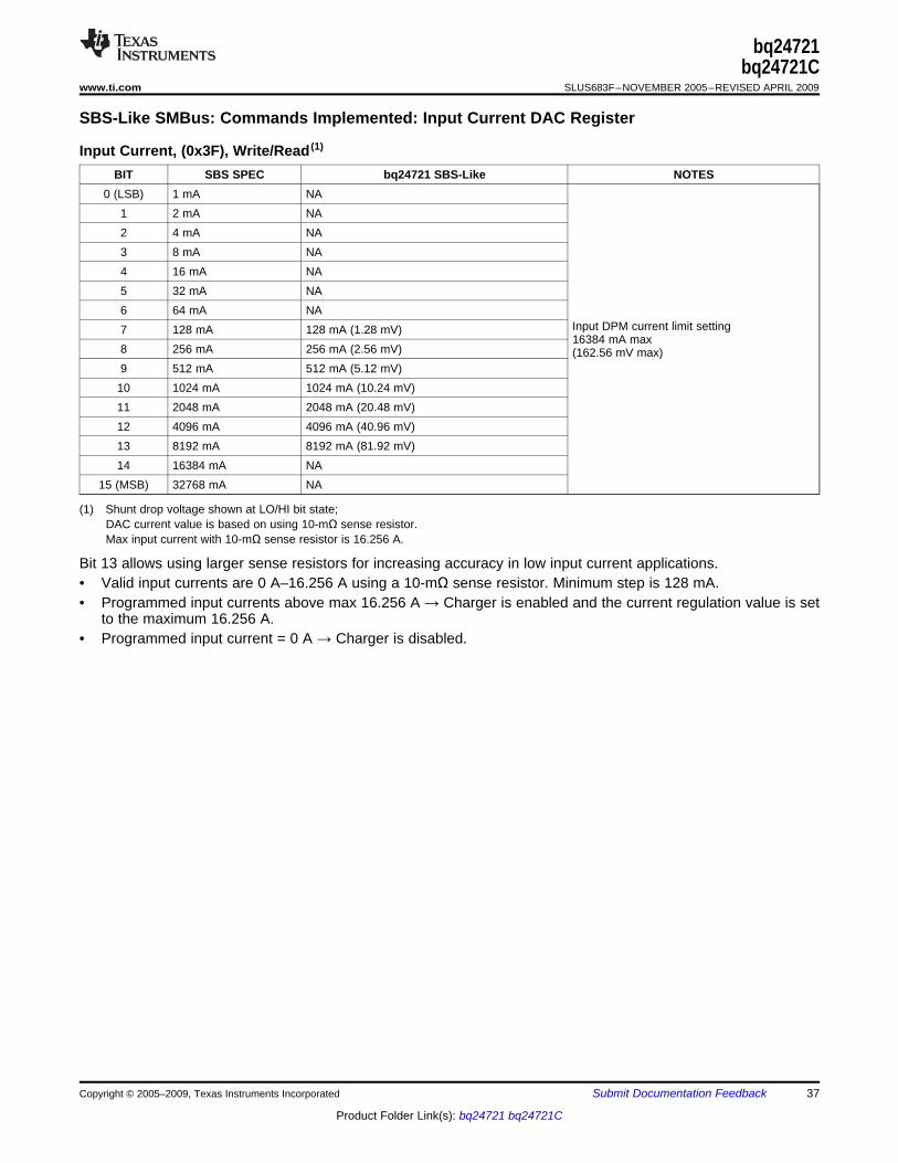
SBS-Like SMBus: Commands Implemented: Input Current DAC Register
Input Current, (0x3F), Write/Read (1)
bq24721bq24721C
www.ti.com.................................................................................................................................................. SLUS683F–NOVEMBER 2005–REVISED APRIL 2009
BIT SBS SPEC bq24721 SBS-Like NOTES0 (LSB) 1 mA NA
1 2 mA NA2 4 mA NA3 8 mA NA4 16 mA NA5 32 mA NA6 64 mA NA
Input DPM current limit setting7 128 mA 128 mA (1.28 mV)16384 mA max
8 256 mA 256 mA (2.56 mV) (162.56 mV max)9 512 mA 512 mA (5.12 mV)
10 1024 mA 1024 mA (10.24 mV)11 2048 mA 2048 mA (20.48 mV)12 4096 mA 4096 mA (40.96 mV)13 8192 mA 8192 mA (81.92 mV)14 16384 mA NA
15 (MSB) 32768 mA NA
(1) Shunt drop voltage shown at LO/HI bit state;DAC current value is based on using 10-mΩ sense resistor.Max input current with 10-mΩ sense resistor is 16.256 A.
Bit 13 allows using larger sense resistors for increasing accuracy in low input current applications.• Valid input currents are 0 A–16.256 A using a 10-mΩ sense resistor. Minimum step is 128 mA.• Programmed input currents above max 16.256 A → Charger is enabled and the current regulation value is set
to the maximum 16.256 A.• Programmed input current = 0 A → Charger is disabled.
Copyright © 2005–2009, Texas Instruments Incorporated Submit Documentation Feedback 37
Product Folder Link(s): bq24721 bq24721C
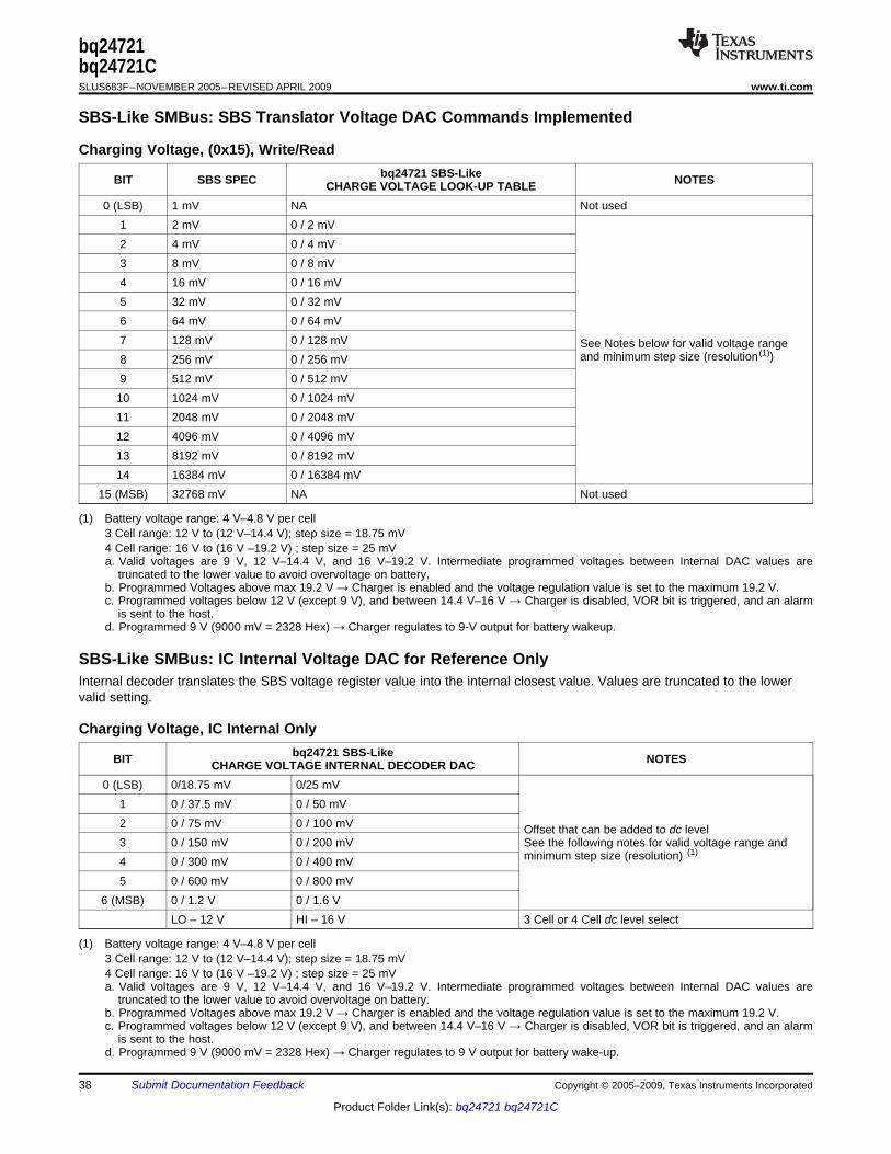
SBS-Like SMBus: SBS Translator Voltage DAC Commands Implemented
Charging Voltage, (0x15), Write/Read
SBS-Like SMBus: IC Internal Voltage DAC for Reference Only
Charging Voltage, IC Internal Only
bq24721bq24721CSLUS683F–NOVEMBER 2005–REVISED APRIL 2009.................................................................................................................................................. www.ti.com
bq24721 SBS-LikeBIT SBS SPEC NOTESCHARGE VOLTAGE LOOK-UP TABLE0 (LSB) 1 mV NA Not used
1 2 mV 0 / 2 mV2 4 mV 0 / 4 mV3 8 mV 0 / 8 mV4 16 mV 0 / 16 mV5 32 mV 0 / 32 mV6 64 mV 0 / 64 mV7 128 mV 0 / 128 mV See Notes below for valid voltage range
and minimum step size (resolution (1))8 256 mV 0 / 256 mV9 512 mV 0 / 512 mV
10 1024 mV 0 / 1024 mV11 2048 mV 0 / 2048 mV12 4096 mV 0 / 4096 mV13 8192 mV 0 / 8192 mV14 16384 mV 0 / 16384 mV
15 (MSB) 32768 mV NA Not used
(1) Battery voltage range: 4 V–4.8 V per cell3 Cell range: 12 V to (12 V–14.4 V); step size = 18.75 mV4 Cell range: 16 V to (16 V –19.2 V) ; step size = 25 mVa. Valid voltages are 9 V, 12 V–14.4 V, and 16 V–19.2 V. Intermediate programmed voltages between Internal DAC values are
truncated to the lower value to avoid overvoltage on battery.b. Programmed Voltages above max 19.2 V → Charger is enabled and the voltage regulation value is set to the maximum 19.2 V.c. Programmed voltages below 12 V (except 9 V), and between 14.4 V–16 V → Charger is disabled, VOR bit is triggered, and an alarm
is sent to the host.d. Programmed 9 V (9000 mV = 2328 Hex) → Charger regulates to 9-V output for battery wakeup.
Internal decoder translates the SBS voltage register value into the internal closest value. Values are truncated to the lowervalid setting.
bq24721 SBS-LikeBIT NOTESCHARGE VOLTAGE INTERNAL DECODER DAC0 (LSB) 0/18.75 mV 0/25 mV
1 0 / 37.5 mV 0 / 50 mV2 0 / 75 mV 0 / 100 mV Offset that can be added to dc level3 0 / 150 mV 0 / 200 mV See the following notes for valid voltage range and
minimum step size (resolution) (1)4 0 / 300 mV 0 / 400 mV5 0 / 600 mV 0 / 800 mV
6 (MSB) 0 / 1.2 V 0 / 1.6 VLO – 12 V HI – 16 V 3 Cell or 4 Cell dc level select
(1) Battery voltage range: 4 V–4.8 V per cell3 Cell range: 12 V to (12 V–14.4 V); step size = 18.75 mV4 Cell range: 16 V to (16 V –19.2 V) ; step size = 25 mVa. Valid voltages are 9 V, 12 V–14.4 V, and 16 V–19.2 V. Intermediate programmed voltages between Internal DAC values are
truncated to the lower value to avoid overvoltage on battery.b. Programmed Voltages above max 19.2 V → Charger is enabled and the voltage regulation value is set to the maximum 19.2 V.c. Programmed voltages below 12 V (except 9 V), and between 14.4 V–16 V → Charger is disabled, VOR bit is triggered, and an alarm
is sent to the host.d. Programmed 9 V (9000 mV = 2328 Hex) → Charger regulates to 9 V output for battery wake-up.
38 Submit Documentation Feedback Copyright © 2005–2009, Texas Instruments Incorporated
Product Folder Link(s): bq24721 bq24721C
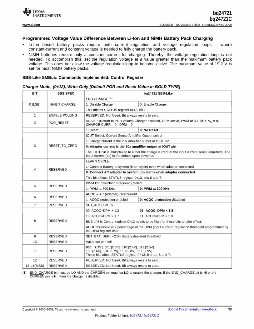
Programmed Voltage Value Difference Between Li-Ion and NiMH Battery Pack Charging
SBS-Like SMBus: Commands Implemented: Control Register
bq24721bq24721C
www.ti.com.................................................................................................................................................. SLUS683F–NOVEMBER 2005–REVISED APRIL 2009
• Li-Ion based battery packs require both current regulation and voltage regulation loops – whereconstant-current and constant voltage is needed to fully charge the battery pack.
• NiMH batteries require only a constant current for charging. Thereby, the voltage regulation loop is notneeded. To accomplish this, set the regulation voltage at a value greater than the maximum battery packvoltage. This does not allow the voltage regulation loop to become active. The maximum value of 19.2 V isset for most NiMH battery packs.
Charger Mode, (0x12), Write-Only [Default POR and Reset Value in BOLD TYPE]BIT SBS SPEC bq24721 SBS-Like
END CHARGE (1)
0 (LSB) INHIBIT CHARGE 1: Disable Charger 0: Enable ChargerThis affects STATUS register 0x13, bit 1.
1 ENABLE POLLING RESERVED: Not Used. Bit always resets to zero.RESET: (Return to POR values) Charger disabled, DPM active, PWM at 300 kHz, VO = 0,2 POR_RESET CHARGE CURR = 0, IDPM = 01: Reset 0: No ResetIOUT Select: Current Sense Amplifier Output select1: Charge current is the 20x amplifier output at IOUT pin
3 RESET_TO_ZERO 0: Adapter current is the 20x amplifier output at IOUT pinThe IOUT pin is multiplexed to either the charge current or the input current sense amplifiers. TheInput current (ac) is the default upon power up.LEARN CYCLE1: Connect Battery to system (learn cycle) even when adapter connected
4 RESERVED0: Connect AC adapter to system (no learn) when adapter connectedThis bit affects STATUS register 0x13, bits 6 and 7.PWM FS: Switching Frequency Select
5 RESERVED1: PWM at 500 kHz 0: PWM at 300 kHzACOC – AC (adapter) Overcurrent
6 RESERVED1: ACOC protection enabled 0: ACOC protection disabled
7 RESERVED SET_ACOC <1:0>00: ACOC=DPM × 1.3 01: ACOC=DPM × 1.510: ACOC=DPM × 1.7 11: ACOC=DPM × 1.9
8 RESERVED Bit 6 of this Control register 0×12 needs to be high for these bits to take effect.ACOC threshold is a percentage of the DPM (input current) regulation threshold programmed bythe DPM register 0×3F.
9 RESERVED SET_BAT_DEPL <2:0> Battery depleted threshold10 RESERVED Value set per cell
000: [2.2V], 001:[2.3V], 010:[2.4V], 011:[2.5V]11 RESERVED 100:[2.6V], 101:[2.7V], 110:[2.8V], 111:[2.9V]
These bits affect STATUS register 0×13, bits 11, 6 and 7.12 RESERVED RESERVED: Not Used. Bit always resets to zero.
13–15(MSB) RESERVED RESERVED: Not Used. Bit always resets to zero.
(1) END_CHARGE bit must be LO AND the CHRGEN pin must be LO to enable the charger. If the END_CHARGE bit is HI or theCHRGEN pin is HI, then the charger is disabled.
Copyright © 2005–2009, Texas Instruments Incorporated Submit Documentation Feedback 39
Product Folder Link(s): bq24721 bq24721C
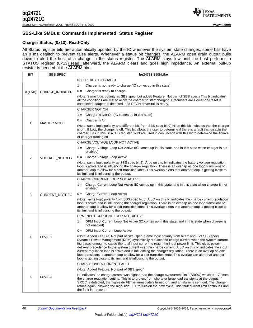
SBS-Like SMBus: Commands Implemented: Status Register
Charger Status, (0x13), Read-Only
bq24721bq24721CSLUS683F–NOVEMBER 2005–REVISED APRIL 2009.................................................................................................................................................. www.ti.com
All Status register bits are automatically updated by the IC whenever the system state changes, some bits havean 8 ms deglitch to prevent false alerts. Whenever a status bit changes, the ALARM open drain output pullsdown to alert the host of a change in the status register. The ALARM stays low until the host performs aSTATUS register (0×13) read, afterward, the ALARM clears and goes high impedance. An external pull-upresistor is needed at the ALARM pin.
BIT SBS SPEC bq24721 SBS-LikeNOT READY TO CHARGE1 = Charger is not ready to charge (IC comes up in this state)0 = Charger is ready to charge0 (LSB) CHARGE_INHIBITED(Note: Same logic polarity as SBS spec, but added Feature, Not part of SBS spec.) This bit indicatesall the conditions are met to allow the charger to start charging. Precursers are Power-on-Reset iscompleted; adapter is detected, and REGN driver rail is ready.CHARGER NOT ON1 = Charger is Not On (IC comes up in this state)0 = Charger is On
1 MASTER MODE(Note: same logic polarity and different bit, from SBS spec bit 0) Hi on this bit indicates that the chargeris on . If Low, the charger is off. This bit allows the user to determine if there is a fault that disable thecharger. Bits in this STATUS register 0x13 are used in conjunction with this bit to determine the sourceof charger turning off.CHARGE VOLTAGE LOOP NOT ACTIVE1 = Charge Voltage Loop Not Active (IC comes up in this state, and in this state when charger is not
enabled)0 = Charge Voltage Loop Active2 VOLTAGE_NOTREG(Note: same logic polarity as SBS spec bit 2). A Lo on this bit indicates the battery voltage regulationloop is active and is influencing the charger regulation. There is an overlap as one loop transitions toanother loop to allow for a soft transition knee. This overlap alerts that another loop is getting close toits limit and is influencing the output.CHARGE CURRENT LOOP NOT ACTIVE1 = Charge Current Loop Not Active (IC comes up in this state, and in this state when charger is not
enabled)0 = Charge Current Loop Active3 CURRENT_NOTREG(Note: same logic polarity from SBS spec bit 3) A LO on this bit indicates the charge current regulationloop is active and is influencing the charger regulation. There is an overlap as one loop transitions toanother loop to allow for a soft transition knee. This overlap alerts that another loop is getting close toits limit and is influencing the output.DPM INPUT CURRENT LOOP NOT ACTIVE1 = DPM Input Current Loop Not Active (IC comes up in this state, and in this state when charger is
not enabled)0 = DPM Input Current Loop Active(Note: Added Feature, Not part of SBS spec. Same logic polarity from bits 2 and 3 of SBS spec)4 LEVEL2Dynamic Power Management (DPM) dynamically reduces the charge current when the system currentincreases enough to cause the total input current to reach the input power limit. This gives powerdelivery precedence to the system current over the charge current. A LO on this bit indicates the inputcurrent regulation loop is active and is influencing the charger regulation. There is an overlap as oneloop transitions to another loop to allow for a soft transition knee. This overlap can alert that anotherloop is getting close to its limit and is influencing the output.CHARGE OVERCURRENT FAULT(Note: Added Feature, Not part of SBS spec.)HI indicates the charge current was higher than the charge overcurrent limit (SROC) which is 1.7 times5 LEVEL3 the charge regulation setting. This is to protect from shorts or large load transients at the output. IfSROC is detected, the high-side FET is immediately turned-off, and an alarm is sent out. The chargerretries again, allowing the high-side FET to turn-on the next cycle. This fault current limit continues untilthe fault is removed.
40 Submit Documentation Feedback Copyright © 2005–2009, Texas Instruments Incorporated
Product Folder Link(s): bq24721 bq24721C
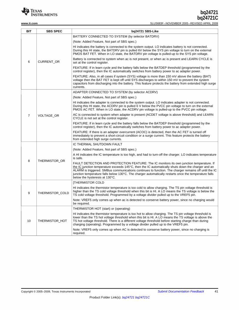
bq24721bq24721C
www.ti.com.................................................................................................................................................. SLUS683F–NOVEMBER 2005–REVISED APRIL 2009
BIT SBS SPEC bq24721 SBS-LikeBATTERY CONNECTED TO SYSTEM (by selector BATDRV)(Note: Added Feature, Not part of SBS spec.)HI indicates the battery is connected to the system output. LO indicates battery is not connected.During this HI state, the BATDRV pin is pulled 6V below the SYS pin voltage to turn on the externalPMOS BAT FET. When in LO state, the BATDRV pin voltage is pulled-up to the SYS pin voltage.Battery is connected to system when ac is not present, or when ac is present and LEARN CYCLE is
6 CURRENT_OR set at the control register.FEATURE: If in learn cycle and the battery falls below the BATDEP threshold (programmed by thecontrol register), then the IC automatically switches from battery power to ac adapter power.FEATURE: Also, in all cases if system (SYS) voltage is more than 150 mV above the battery (BAT)voltage then the BAT FET is kept off until SYS discharges to within 150 mV to prevent the systemcapacitors from discharging into the battery. This feature protects the battery from extended high surgecurrents.ADAPTER CONNECTED TO SYSTEM (by selector ACDRV)(Note: Added Feature, Not part of SBS spec.)HI indicates the adapter is connected to the system output. LO indicates adapter is not connected.During this HI state, the ACDRV pin is pulled 6 V below the PVCC pin voltage to turn on the externalPMOS AC FET. When in LO state, the ACDRV pin voltage is pulled-up to the PVCC pin voltage.AC is connected to system when adapter is present (ACDET voltage is above threshold) and LEARN7 VOLTAGE_ORCYCLE is not set at the control register.FEATURE: If in learn cycle and the battery falls below the BATDEP threshold (programmed by thecontrol register), then the IC automatically switches from battery power to ac adapter power.FEATURE: If there is an adapter overcurrent (ACOC) is detected, then the AC FET is turned offimmediately to prevent a short-circuit condition or a surge current. This feature protects the batteryfrom extended high surge currents.IC THERMAL SHUTDOWN FAULT(Note: Added Feature, Not part of SBS spec.)A HI indicates the IC temperature is too high, and had to turn-off the charger. LO indicates temperatureis safe.
8 THERMISTOR_ORFAULT DETECTION AND PROTECTION FEATURE: The IC monitors its own junction temperature. Ifthe IC junction temperature exceeds 145°C, then the IC automatically shuts down the charger and anALARM is triggered. SMBus communications continues to function. The charger remains off until the ICjunction temperature falls below 130°C. The charger automatically restarts once the temperature fallsbelow the hysteresis at 130°C.[THERMISTOR COLDHI indicates the thermistor temperature is too cold to allow charging. The TS pin voltage threshold ishigher than the TS cold voltage threshold when this bit is HI. A LO means the TS voltage is below the9 THERMISTOR_COLD TS cold voltage threshold. Programmed by a voltage divider pulled up to the VREF5 pin.Note: VREF5 only comes up when ac is detected to conserve battery power, since no charging wouldbe required.THERMISTOR HOT (start) or (operating)HI indicates the thermistor temperature is too hot to allow charging. The TS pin voltage threshold islower than the TS hot voltage threshold when this bit is HI. A LO means the TS voltage is above the
10 THERMISTOR_HOT TS hot voltage threshold. There is a different voltage threshold before starting charge than duringcharging (operating). Programmed by a voltage divider pulled up to the VREF5 pin.Note: VREF5 only comes up when AC is detected to conserve battery power, since no charging isrequired.
Copyright © 2005–2009, Texas Instruments Incorporated Submit Documentation Feedback 41
Product Folder Link(s): bq24721 bq24721C
bq24721bq24721CSLUS683F–NOVEMBER 2005–REVISED APRIL 2009.................................................................................................................................................. www.ti.com
BIT SBS SPEC bq24721 SBS-LikeBATTERY VOLTAGE LOW (battery depleted)(Note: Added Feature, Not part of SBS spec.)This bit goes HI when the sensed BAT voltage is below the Battery Depleted threshold programmed bythe CONTROL register 0x12, bits 9, 10, and 11. The programmed voltage is per cell; therefore, multiply
11 THERMISTOR_UR by the number of cells set by the programmed battery voltage regulation DAC, register 0x15. [3 cell forvoltages between 12 V-14.4 V; and 4 cell for voltages between 16 V-19.2 V].FEATURE: the BATDRV is turned off when the battery voltage falls below the BATDEP threshold, andthe AC DRV is turned on if adapter is connected, and had previously been in LEARN Cycle (bit 4 ofCONTROL register, 0x12).VOR, VOLTAGE OUT OF RANGE (Note: moved function from bit7 of SBS spec) A HI indicates thevoltage DAC value from register 0x15 is out of the valid DAC voltage range. The IC either disables thecharge if below, or stays at the maximum possible programmed voltage (19.2 V) according to thefollowing. Valid voltage DAC range and effect.
• Valid voltages are 9 V, 12 V –14.4 V, and 16 V–19.2 V. Intermediate programmed voltagesbetween Internal DAC values are truncated to the lower value to avoid overvoltage on battery.12 ALARM_INHIBITED
• Programmed Voltages above max 19.2 V → Charger is enabled and the voltage regulation valueis set to the maximum 19.2 V.
• Programmed voltages below 12 V (except 9 V), and between 14.4 V–16 V → Charger isdisabled, VOR bit is triggered, and an alarm sent to host.
• Programmed 9 V (9000 mV = 2328 Hex) → Charger regulates to 9-V output for battery wake-up.ADAPTER VOLTAGE BELOW BATTERY PACK VOLTAGE(Note: Added Feature, Not part of SBS spec.) A HI on this bit indicates the battery voltage is above theadapter voltage (BAT pin > ACP pin).13 POWER_FAILFEATURE: If the input falls below 150 mV above the Battery voltage, the BYPASS FET immediatelyturns off to prevent reverse discharge of the battery into the adapter. There is an 8 ms deglitch and100 mV to hysteresis before allowing the BYPASS FET to turn-on.BATTERY DETECTED ( through thermistor pin)FEATURE: HI indicates a battery is detected through the TS pin. The TS pin voltage threshold is lowerthan the TS battery detect threshold when this bit is HI. A LO means the TS voltage is above the TSbattery detect threshold. A resistor to ground inside the battery is used to distinguish a good batteryfrom a bad battery as well. Programmed by a voltage divider pulled up to the VREF5 pin.Note: VREF5 only comes up when ac is detected to conserve battery power, since no charging is
14 BATTERY PRESENT required.(Note: Added Feature. This is used for detecting proper battery connected by selecting the proper validresistance. This is need to be ORed for dual battery pack chargers to make feature optimal. Thisfeature also is used as a safety feature to stop charge immediately when the battery pack is notdetected – this allows a faster response time by autonomously terminating charge when no battery isdetected, as opposed to waiting until the host detects the battery is removed and then alerting thecharger.AC ADAPTOR DETECTEDThis bit is HI when the adapter is detected (ACDET pin voltage is above the acdetect threshold of2.4V). The voltage can be programmed by an external resistor divider from adapter input to ground.15 AC_PRESENT Charge is not allowed until the ACDET threshold is exceeded. VREF5 LDO output only turns on when(MSB) the ACDET threshold is exceeded (adapter detected).REGN POR and SMBus communication begins soon after the ACDET threshold is above 1.2 V andthe VCC is above 6.5 V.
42 Submit Documentation Feedback Copyright © 2005–2009, Texas Instruments Incorporated
Product Folder Link(s): bq24721 bq24721C

ELECTRICAL CHARACTERISTICS
t(BUF)
STOP
START
1 98732
1 98732
ACK
ACK
SCL
SCL
SDA
SDA
START
tw(L)
tw(H)
tsu(STA)
tsu(DAT)
tsu(STOP)
th(STA) th(DAT)
th(DAT)
tf
tf
tr
tr
STOP
SCL
SDA
bq24721bq24721C
www.ti.com.................................................................................................................................................. SLUS683F–NOVEMBER 2005–REVISED APRIL 2009
7 Vdc ≤ V(VCC) ≤ 24 Vdc, –20°C < TJ < 125°C, ref = AGND (unless otherwise noted).
PARAMETER MIN TYP MAX UNITSMBus TIMING CHARACTERISTICStR SCLK/SDATA rise time 1 µstF SCLK/SDATA fall time 300 nstW(H) SCLK pulse width high 4 50 µstW(L) SCLK Pulse Width Low 4.7 µstSU(STA) Setup time for START condition 4.7 µstH(STA) START condition hold time after which first clock pulse is generated 4 µstSU(DAT) Data setup time 250 nstH(DAT) Data hold time 300 nstSU(STOP) Setup time for STOP condition 4 µst(BUF) Bus free time between START and STOP condition 4.7 µsFS(CL) Clock Frequency 10 100 kHzALARM LOGIC TIMING CHARACTERISTICStALM Time delay from status register bit toggling to ALERT: LO → HI transition 6 10 msHOST COMMUNICATION FAILUREttimeout SMBus bus release timeout 25 35 mstBOOT Deglitch for watchdog reset signal 10 mstWDI Watchdog timeout period 140 170 200 sOUTPUT BUFFER CHARACTERISTICSV(SDAL) Output LO voltage at SDA, I(SDA) = 3 mA 0.4 V
Figure 60.
Copyright © 2005–2009, Texas Instruments Incorporated Submit Documentation Feedback 43
Product Folder Link(s): bq24721 bq24721C
FUNCTIONAL DESCRIPTION
SMBus Overview
SMBus Address
Internal Register Map
SMBus Bus Release
SMBus Communication Protocol
bq24721bq24721CSLUS683F–NOVEMBER 2005–REVISED APRIL 2009.................................................................................................................................................. www.ti.com
An SMBus communication port provides a simple way for an SMBus compatible host to access system statusinformation and reset fault modes. Functioning as a SLAVE port enables SMBus compatible hosts to WRITE tointernal registers or READ from internal registers. The bq24721 SMBus port is a 2-wire bidirectional interfaceusing SCL (clock) and SDA (data) pins; the SDA pin is open drain and requires an external pull-up. The SMBusis designed to operate at SCL frequencies up to 100 kHz. The standard 8 bit command is supported, the CMDpart of the sequence is the 8 bit register address which is READ from or WRITE to. The bq24721 does notsupport packet error correction, PEC, as a mechanism to confirm proper communication between it and the host.
The SMBus specification contains several global addresses, to which the slaves on the bus are required torespond. The bq24721 responds to the SBS charger addresses of 0×12 for writes and 0×13 for reads. Thebq24721 only responds (ACK) to the above listed addresses, and does (NACK) not respond to any otheraddress.
BITBYTE
MSB 6 5 4 3 2 1 LSBbq24721 SMBus WRITE ADDRESS SBS Charger 0 0 0 1 0 0 1 0bq24721 SMBus READ ADDRESS SBS Charger 0 0 0 1 0 0 1 1COMMAND 0 0 0 1 C3 C2 C1 C0I/O DATA BUS D7 D6 D5 D4 D3 D2 D1 D0
The status data and control data is referenced by the following Commands.COMMAND R/W REGISTER DESCRIPTION
0x12 R/W Charger Mode0x13 R Charger Status0x14 R/W Charging Current0x15 R/W Charging Voltage0x3F R/W Input Current
The bq24721 SMBus engine does not create START or STOP states on the SMBus bus during normaloperation. However, if a 2 second (typical) SDA low timeout is exceeded the bq24721 releases the bus, thuscreating a stop condition.
The following conventions is used when describing the communication protocol.CONDITION CODE
START sent from host SSTOP sent from host Pbq24721 SMBus slave address sent from host, bus direction set from host to bq24721 (WRITE) hA0bq24721 register address sent from bq24721, bus direction is from bq24721 to host (READ) hA1Non-valid SMBus slave address sent from host hA_NValid bq24721 register address sent from host HCMDNonvalid bq24721 register address sent from host HCMD_NI/O data byte (8 bits) sent from host to bq24721 hDATAI/O data byte (8 bits) sent from bq24721 to host bqDATAAcknowledge (ACK) from host hA
44 Submit Documentation Feedback Copyright © 2005–2009, Texas Instruments Incorporated
Product Folder Link(s): bq24721 bq24721C
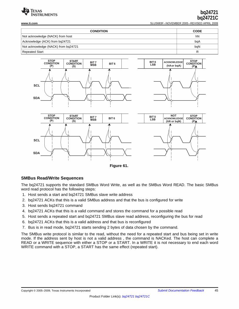
STOPCONDITION
(P)
STARTCONDITION
(S)
BIT 7MSB BIT 6
BIT 0LSB
ACKNOWLEDGE
(hAor bqA)
STOPCONDITION
(P)
SCL
SDA
STOPCONDITION
(P)
STARTCONDITION
(S)
BIT 7MSB
BIT 6BIT 0LSB
NOTACKNOWLEDGE
(hN or bqN)
STOPCONDITION
(P)
SCL
SDA
SMBus Read/Write Sequences
bq24721bq24721C
www.ti.com.................................................................................................................................................. SLUS683F–NOVEMBER 2005–REVISED APRIL 2009
CONDITION CODENot acknowledge (NACK) from host hNAcknowledge (ACK) from bq24721 bqANot acknowledge (NACK) from bq24721 bqNRepeated Start R
Figure 61.
The bq24721 supports the standard SMBus Word Write, as well as the SMBus Word READ. The basic SMBusword read protocol has the following steps:1. Host sends a start and bq24721 SMBus slave write address2. bq24721 ACKs that this is a valid SMBus address and that the bus is configured for write3. Host sends bq24721 command4. bq24721 ACKs that this is a valid command and stores the command for a possible read5. Host sends a repeated start and bq24721 SMBus slave read address, reconfiguring the bus for read6. bq24721 ACKs that this is a valid address and that bus is reconfigured7. Bus is in read mode, bq24721 starts sending 2 bytes of data chosen by the command.
The SMBus write protocol is similar to the read, without the need for a repeated start and bus being set in writemode. If the address sent by host is not a valid address , the command is NACKed. The host can complete aREAD or a WRITE sequence with either a STOP or a START. In a WRITE it is not necessary to end each wordWRITE command with a STOP, a START has the same effect (repeated start).
Copyright © 2005–2009, Texas Instruments Incorporated Submit Documentation Feedback 45
Product Folder Link(s): bq24721 bq24721C

Valid Write Sequences
Word Write
Valid Read Sequences
SMBus Word Read
Nonvalid Sequences
Attempt to Specify Nonallowed Command
bq24721bq24721CSLUS683F–NOVEMBER 2005–REVISED APRIL 2009.................................................................................................................................................. www.ti.com
The bq24721 always ACKs its own address. If the CMD points to an allowable READ or WRITE data bq24721writes the command into its command register and send an ACK. If the CMD points to an nonallowed commandbq24721 does NOT write the command into its command register and sends a NACK.
S hA0 bqA
S hA0 bqA hCMD_N bqN
The data is written to a control register at the end of the ACK after the second byte in the sequence. If an wordwrite sequence is intrupted by a STOP or START, no data is written to the device. The host can cancel a WRITEby sending a STOP or START before the trailing edge of ACK clock pulse.
S hA0 bqA hCMD bqA hDATA bqA hDATA bqA P
The bq24721 only ACKs its READ address if it occurs following a repeated start where the high SCL clock timeis less then the tW(H), MAX of 50 µs. Upon receiving hA1, bq24721 outputs 2 bytes of data as indicated by thepreceding command. The command sequence is terminated by a STOP. The START and the STOP both act aspriority interrupts. If the host has been interrupted and is not sure where it left off, it sends a STOP and resets thebq24721 state machine to the Idle state. Once in idle state, bq24721 ignores all activity on the SCL and SDAlines until it receives a START. If a read sequence is terminated early by a START or STOP, the entire sequencemust be restarted by the host for valid data.
S hA0 bqA hCMD bqA R hA1 bqA bqDATA hA bqDATA hN P
A valid Command is required to write to the bq24721, and a valid Command is required to specify the data to beread. Once a read command is received the register data for the specified command is output to the host.
START and non-hA0 or non-hA1 Address
A START followed by an address which is not bqA0 or bqA1 is NACKED.
If the CMD points to a nonallowed command (reserved registers) , bq24721 sends a NACK back to the host.Note that bq24721 NACKS whether a stop is sent or not.
S hA0 bqA hCMD_N bqN
S hA_N bqN
46 Submit Documentation Feedback Copyright © 2005–2009, Texas Instruments Incorporated
Product Folder Link(s): bq24721 bq24721C

Status and Control Registers
DESIGN CALCULATIONS EXAMPLE
System Requirements (See Figure 52)
Select the Sense Resistors
P(RSENSE_INPUT) R(SENSE_DPM) I(INPUT_REG)2 10 m 80 W
19 V
2
177 mW(3)
P(RSENSE_CHRG) R(SENSE_CHRG) I(INPUT_REG)2 10 m (4A)2
160 mW(4)
Select Switching Frequency:
Selecting the Output Inductor
Lout
VI max V(BAT) minV(BAT)min
VImax 1
fSW
40% I(CHRG_REG) (5)
bq24721bq24721C
www.ti.com.................................................................................................................................................. SLUS683F–NOVEMBER 2005–REVISED APRIL 2009
The SMBUS-Like communication engine allows easy access to system status data contained in internal registersthat contain information on current status for system power selection, charger mode and fault conditions. Anychange on the state of those bits generates an interrupt request to the host (ALARM pin = HI).
Table 2. Status Register Latched BitsACOC/CHGOC LATCHES
SET RESET CONTROL LOGIC ACTION AT DETECTIONLatches data going to status register, disables further updates on statusCharger overcurrent detected Host read register register CHGOC bit until reset.Latches data going to status register, disables further updates on ACOC bitAC adapter overcurrent detected Host read register until reset.
For a system using a 20 V, ±5%, 80-W adapter, use a 12.6-V (3-cell) or 16.8-V (4-cell) battery, with a chargecurrent regulation threshold of 4 A, and a precharge/wake-up current of 300 mA. The battery pack voltage variesfrom a deeply discharged voltage of 3-V per cell, and up to a regulation voltage of 4.2-V per cell— giving rangesof 9-V to 12.6-V for 3-cell batteries, and 12-V to 16.8-V for 4-cell batteries.
The SBS specification was done based on a 10-mΩ sense resistor. The charger operates with low resistance. Ifthe thermal dissipation is tolerable, a larger sense resistor (such as 20 mΩ) is used to provide greater accuracyin the regulation and current sense amplifier.
For this design example, a 10-mΩ sense resistor is selected for both the input current and output charge currentsense resistors.
The power dissipation for each sense resistor is:
where the maximum input current is the input power limit divided by the input voltage.
A 1 W, 2010 rating provides sufficient margin.
Select switching frequency = 300 kHz.
Inductor is designed for current ripple 40% of the 4-A regulation threshold (I(RIPPLE) = 1.6 A).
Where the VImax is the maximum input voltage, V(BAT)min is the minimum battery voltage, and fSW is theswitching frequency.
Copyright © 2005–2009, Texas Instruments Incorporated Submit Documentation Feedback 47
Product Folder Link(s): bq24721 bq24721C
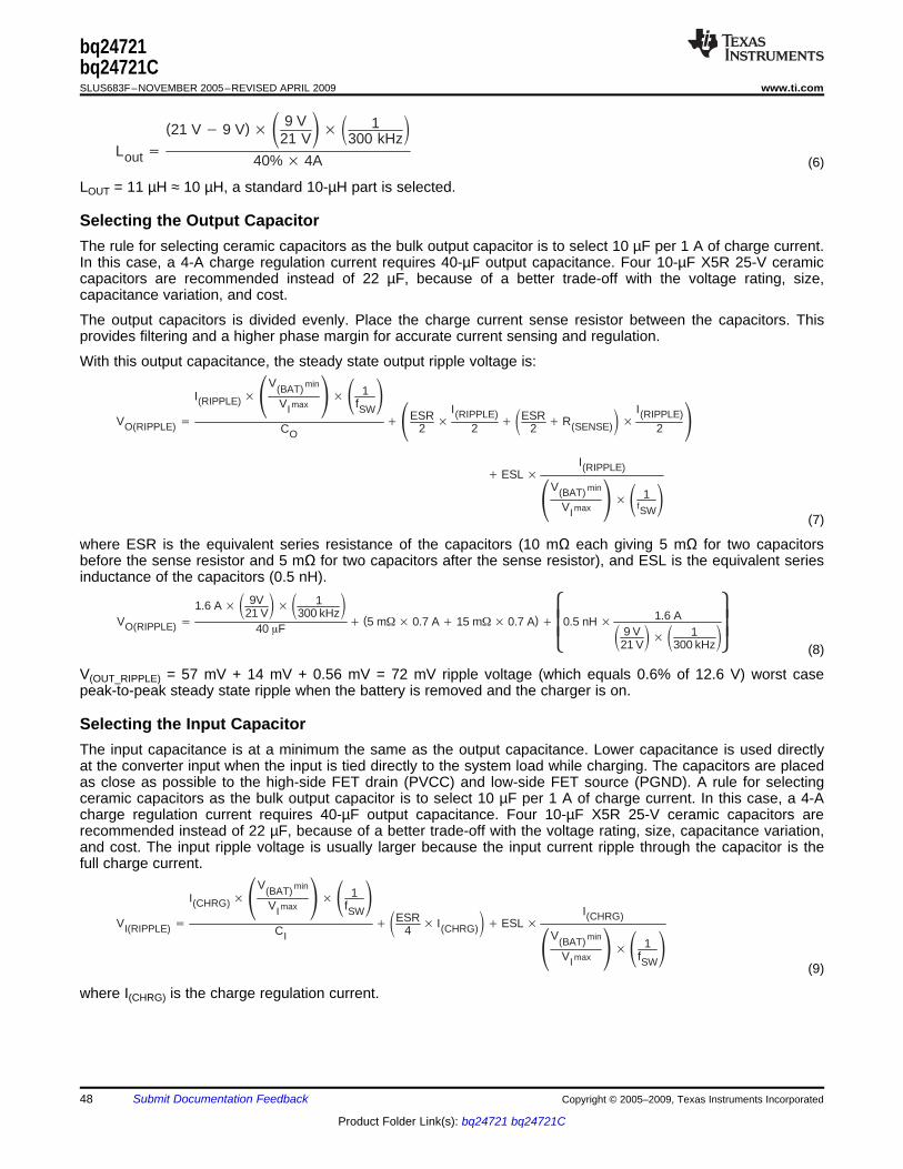
Lout
(21 V 9 V) 9 V21 V 1
300 kHz
40% 4A (6)
Selecting the Output Capacitor
VO(RIPPLE)
I(RIPPLE) V(BAT) min
VI max 1
fSW
COESR
2
I(RIPPLE)2
ESR2
R(SENSE)I(RIPPLE)
2
ESL I(RIPPLE)
V(BAT) min
VI max 1
fSW
(7)
VO(RIPPLE) 1.6 A 9V
21 V 1
300 kHz
40 F (5 m 0.7 A 15 m 0.7 A)
0.5 nH 1.6 A
9 V21 V 1
300 kHz (8)
Selecting the Input Capacitor
VI(RIPPLE)
I(CHRG) V(BAT) min
VI max 1
fSW
CI ESR
4 I(CHRG) ESL
I(CHRG)
V(BAT) min
VI max 1
fSW
(9)
bq24721bq24721CSLUS683F–NOVEMBER 2005–REVISED APRIL 2009.................................................................................................................................................. www.ti.com
LOUT = 11 µH ≈ 10 µH, a standard 10-µH part is selected.
The rule for selecting ceramic capacitors as the bulk output capacitor is to select 10 µF per 1 A of charge current.In this case, a 4-A charge regulation current requires 40-µF output capacitance. Four 10-µF X5R 25-V ceramiccapacitors are recommended instead of 22 µF, because of a better trade-off with the voltage rating, size,capacitance variation, and cost.
The output capacitors is divided evenly. Place the charge current sense resistor between the capacitors. Thisprovides filtering and a higher phase margin for accurate current sensing and regulation.
With this output capacitance, the steady state output ripple voltage is:
where ESR is the equivalent series resistance of the capacitors (10 mΩ each giving 5 mΩ for two capacitorsbefore the sense resistor and 5 mΩ for two capacitors after the sense resistor), and ESL is the equivalent seriesinductance of the capacitors (0.5 nH).
V(OUT_RIPPLE) = 57 mV + 14 mV + 0.56 mV = 72 mV ripple voltage (which equals 0.6% of 12.6 V) worst casepeak-to-peak steady state ripple when the battery is removed and the charger is on.
The input capacitance is at a minimum the same as the output capacitance. Lower capacitance is used directlyat the converter input when the input is tied directly to the system load while charging. The capacitors are placedas close as possible to the high-side FET drain (PVCC) and low-side FET source (PGND). A rule for selectingceramic capacitors as the bulk output capacitor is to select 10 µF per 1 A of charge current. In this case, a 4-Acharge regulation current requires 40-µF output capacitance. Four 10-µF X5R 25-V ceramic capacitors arerecommended instead of 22 µF, because of a better trade-off with the voltage rating, size, capacitance variation,and cost. The input ripple voltage is usually larger because the input current ripple through the capacitor is thefull charge current.
where I(CHRG) is the charge regulation current.
48 Submit Documentation Feedback Copyright © 2005–2009, Texas Instruments Incorporated
Product Folder Link(s): bq24721 bq24721C
VI(RIPPLE) 4 A 9 V
21 V 1
300 kHz
40 F 10 m
4 4 A 0.5 nH 4 A
9 V21 V
1300 kHz
(10)
Selecting the High-Side Power MOSFET, Q3
P(CON) I(CHRG)2
V(BAT) max
VI min
rDS(on)
(11)
P(SW) I(CHRG) VI min
Q(GS) Q(GD)
i(G)
fSW
(12)
P(CON) (4A )2 16.8 V
19 V (12 m) 180 mW
P(SW) 4 A 19 V (5 nC 7 nC)IA
300 kHz 274 mW
P(GD) 18 nC 19 V 300 kHz 103 mW(13)
Selecting the Low-Side Power MOSFET, Q4
bq24721bq24721C
www.ti.com.................................................................................................................................................. SLUS683F–NOVEMBER 2005–REVISED APRIL 2009
VI(RIPPLE) = 143 mV + 10 mV + 1.4 mV = 154 mV which is 0.77% of the nominal 20-V input voltage.
Note that a single 10-µF capacitor is used from PVCC (close to the drain of the high-side FET) to PGND, whenthe system load is connected to PVCC, because the capacitors on the system rail provide the hold-upcapacitance needed.
The high-side power MOSFET should be an NMOS power MOSFET with a standard voltage rating of 30 V tosupport the 20-V input voltage. The current carrying capability should be at least 2x the maximum charge current.Both the rDS(on) and the gate charge contribute to the power dissipation, while the worst case condition occurs atmax duty cycle (minimum input voltage and maximum battery voltage). The gate drive losses are the onlycomponent that directly dissipate heat in the charger IC.
The FDS6680A was selected. The FDS6680A is a NMOS, 30-V, 12-mΩ device in an SO-8 package.
The conduction losses equal:
where the charger’s 6-V gate drive voltage helps reduce the rDS(on) for lower conduction losses.
The first order approximation switching losses equal:
and the gate drive losses are:P(GD) = Q(GTOT) × VImim x fSW.
Where G(GS) is the gate charge from threshold current conducts until full charge current conducts; Q(GD) is themiller charge where the drain voltage drops, and the Q(GTOT) is the total gate charge form off to fully-enhancedon. The full input voltage is used for gate drive calculation because the internal gate drive regulator dissipatesthe drop from input voltage to the 6-V output voltage which must be added to charging the gates to 6-V everycycle.
The low-side power MOSFET should be an NMOS power MOSFET with a standard voltage rating of 30 V tosupport the 20-V input voltage. The current carrying capability should be at least 2x the maximum charge current.By nature of the synchronous rectifier operation, the drain-to-source voltage is always low at full charge currentwhen the low-side FET turns on—this makes switching losses insignificant, except for the reverse recovery and
Copyright © 2005–2009, Texas Instruments Incorporated Submit Documentation Feedback 49
Product Folder Link(s): bq24721 bq24721C
P(CON) I(CHRG)2
V(BAT) max
VI min
rDS(on)
(14)
P(CON) (4A )2 1 9 V
21 V (9 m) 109 mW
P(SW) 21 V 21 nC 300 kHz 4 A 0.8 V 2 30 ns 300 kHz 132 mW 57.6 mW 190 mW
P(GD) 26 nC 21 V 300 kHz 164 mW(15)
Power MOSFET Thermal Limit Verification
T(LOWSIDE) RthetaJA P(LOSS_LOW_SIDE)50oC
W (109 mW 57.6 mW 164 mW) 16oC
(16)
T(HIGHSIDE) RJA P(LOSS_HIGH_SIDE)
50oCW (180 mW 274 mW 103 mW 134 mW) 35oC
(17)
Optional Schottky Diode across Low-Side FET
bq24721bq24721CSLUS683F–NOVEMBER 2005–REVISED APRIL 2009.................................................................................................................................................. www.ti.com
dead-time contributors that arise from letting the body-diode conduct. The conduction losses and gate drivelosses are the dominant power dissipation; while, the worst case condition occurs at minimum duty cycle(maximum input voltage and minimum battery voltage). The gate drive losses are the only component thatdirectly dissipate heat in the charger IC. Note that the reverse recovery losses are included in this calculation, butthe dissipation occurs in the high-side power MOSFET.
The FDS6670A was selected. The FDS6670A is an NMOS, 30-V, 12-mΩ device in an SO-8 package.
The conduction losses equal:
where the charger’s 6-V gate drive voltage helps reduce the rDS(on) for lower conduction losses.
The first order approximation switching losses are dominated by reverse recovery losses and dead-time lossesgiven by:
P(SW) = VImax × Q(RR) × fSW + I(CGRG) × V(F) × 2 × t(dead-time) x fSW
and the gate drive losses are :P(GD) = Q(GTOT) × VImim x fSW.
Where t(dead-time) is the dead-time where both FETs are off on either edge, Q(RR) is the reverse recovery charge,Q(GTOT) is the total gate charge form off to fully-enhanced on. The full input voltage is used for gate drivecalculation because the internal gate drive regulator dissipates the drop from input voltage to the 6-V outputvoltage which must be added to charging the gates to 6 V every cycle.
The thermal limit verification allows for a 40°C temperature rise from 85°C ambient to 124°C silicon junctiontemperatures. For SO-9, the RθJA is 50°C/W.
The low-side power FET expected temperature rise is:
The high-side power FET expected temperature rise is:
An optional Schottky diode can be used across the low-side power MOSFET (with cathode to drain and anode tosource) to help reduce both the V(F) losses and reverse recovery losses. The Schottky diode is selected on thebasis of the V(F) at I(CHRG), but a power rating for the full current is not required since the Schottky primarilyconducts during the dead-times, which is a fraction of the total switching period.
Power loss for the Schottky are:P(SW) = I(CHRG) × VF × 2 × t(dead-time) x fSW = 4 A × 0.5 V × 2 × 30 ns × 300 kHz = 36 mW
50 Submit Documentation Feedback Copyright © 2005–2009, Texas Instruments Incorporated
Product Folder Link(s): bq24721 bq24721C
Selecting the System Power Selector Power MOSFETs, Q1, Q2, Q5
Calculate the Bootstrap Capacitor
C(BTST) minQ(GTOT)
V(DROP) max
18 nC0.5 V
36 nF(18)
I(DBTST_RATING) minQ(GTOT)
Ts
18 nC3.33 s
5.4 mA(19)
Calculate the ACDET Programming Resistors
Using the equation:V(ADAPT_DET) 1.2 V
R3 R4R4
bq24721bq24721C
www.ti.com.................................................................................................................................................. SLUS683F–NOVEMBER 2005–REVISED APRIL 2009
The system power selector power MOSFETs (Q1, Q2, Q5) must be PMOS power MOSFETs with a standardvoltage rating of 30 V to support the 20-V input voltage, and must have a low rDS(on) to minimize conductionlosses. The continuous current carrying capability should be at least 2x the maximum charge current. Both therDS(on) and the gate charge contribute to the power dissipation, while the worst case condition occurs at max dutycycle (minimum input voltage and maximum battery voltage). The gate drive losses are the only component thatdirectly dissipate heat in the charger IC.
The SI4435 was selected for Q1, Q2, and Q5. The SI4435 is a PMOS, 30-V, 35-mΩ device in an SO-8 package.
The conduction losses equal:P(CON) = I(RMS)
2 × rDS(on),I(RMS_Q1) = I(RMS_Q2) = I(RMS_Q5) = I(SYS)max
where I(RMS) is the RMS current expected for each MOSFET, and I(SYS)max is the maximum continuous systemcurrent.
Note that for Q1, the charge current is not used because the charge current drops to zero as the system current(I(SYS)max) equals or exceeds the programmed input current DAC threshold (IDPM). This is assuming the typicalcase where I(SYS)max > I(DPM).
The system power selector’s -6-V gate drive voltage helps reduce the rDS(on) for lower conduction losses.
The minimum bootstrap capacitor is calculated by the high-side turn-on charge requirements per cycle and thegate drive voltage required. The total gate charge for the FDS6680A high-side power FET is Q(GTOT) = 18 nC,and the maximum gate drive voltage drop allowed is V(DROP) = 0.5 V. The switching frequency of 300 kHz gives acycle period of 3.33 µs.
Select C(BTST) = C12 = 100 nF = 0.1 µF. Connect C12 between the PH and the BTST pins. Also connect abootstrap Schottky diode, D2 , from the REGN pin to the BTST pin. The current rating for the bootstrap diode,D2, is determined by:
Use a 100-mA rated Schottky diode.
An optional 4.7-Ω bootstrap resistor is placed between the BTST pin and the node where C12 and D2 areconnected, in order to minimize ringing by lowering slew rate on the PH node voltage. For lower gate chargeFETs, a larger resistor value can be used up to 10 Ω or 15 Ω. Using larger resistor values increase the switchinglosses, and lower the efficiency.
The adapter is detected when the ACDET pin voltage (sensed adapter input voltage scaled down by resistordivider) exceeds the 1.2 V. The adapter voltage threshold is set to a value less than the minimum adaptervoltage, and higher than the maximum battery pack voltage. [Important: don’t set the value less than themaximum battery pack voltage, otherwise adapter removal is never detected when the battery is connected, andthe battery pack could potentially be drained when no adapter is present]. For this design example, VImin = 19 V,V(BAT) = 16.8 V; therefore, select an adapter detect voltage of V(ADAPT_DET) = 18 V.
and setting V(ADAPT_DET) = 18 V, and selecting (R3 + R4) ≈ 500 Ω.Calculate the standard 1% resistor values of R4 = 33.2 kΩ, and R4 = 464 kΩ.
Copyright © 2005–2009, Texas Instruments Incorporated Submit Documentation Feedback 51
Product Folder Link(s): bq24721 bq24721C

Calculate the ISYNSET Programming Resistor
IL
VI max V(BAT) minV(BAT)min
VImax 1
fSW
Lout (20)
IL (21 V 9 V) 9 V
21 V 1
300 kHz
10 H (21)
The worst case inductor current ripple is ΔIL = 1.71 A. To set the I(SYNSET) threshold to a value betweenIL2
:
R12 R(SYNSET)1 V 500
I(SYNSET) R(SENSE)
1 V 500 1.5 A 10 m
33 k.(22)
Calculate the Thermistor Sense, TS, Programming Resistors
R(VREF_TS) R5 R(TH_C) R(TH_H) VREF5 V(LTF) V(HTF)
V(LTF) V(HTF) R(TH_C) R(TH_H)
(23)
( )( ) ( ) ( ) ( )
´ ´ ´ -= =
´ ´ + ´ ´ - ´ ´ - ´ ´
(TH_C) (TH_H) (HTF) (LTF)
(TS_AGND) 13
(TH_H) (LTF) (TH_C) (LTF) (HTF) (TH_C) (HTF) (TH_H) (LTF) (HTF)
R R VREF5 V VR R
R V VREF5 R V V R V VREF5 R V V
V(NO_PACK)VREF5 R13
(R5 R13)
5 V 130 k(15.8 k 130 k)
4.458 V.(25)
bq24721bq24721CSLUS683F–NOVEMBER 2005–REVISED APRIL 2009.................................................................................................................................................. www.ti.com
The inductor current ripple is defined by:
where the VImax is the maximum input voltage, V(BAT)min is the minimum battery voltage, and fSW is theswitching frequency.
and ΔIL . Set I(SYNSET) = 1.5 A. R(SYNSET) is calculated by the following equation:
The TS comparator programming resistors need the cold pack temperature to disable charge defined, and thehot pack temperature to disable charge defined. The battery cell manufacturer defines the limits. For thisexample, the pack charging temperature limits are: cold temperature = T(COLD) = 0°C, and hot temperatureT(HOT) = 45°C. The charger is not allowed to charge at these temperatures and outside this range, to protect thebattery pack.
Using an industry standard Semitec 202AT NTC Thermistor, the thermistor cold temperature resistance isR(TH_C) = 64.88 kΩ; and the thermistor hot temperature resistance of R(TH_H) = 8.716 kΩ. These values are foundin the 202AT thermistor manufacturer’s data sheet.
The comparator voltage cold limit threshold is V(LTF) = 73.5% of VREF5 = 0.735 × 5 V = 3.675 V, whereVREF5 = 5 V. Likewise, the comparator voltage hot limit threshold is V(HTF) = 34.4% of VREF5 = 0.344 × 5 V =1.72 V.
Since the internal references are with respect to VREF5, R5 is connected from the VREF5 pin to the TS pin, andconnect R13 from the TS pin to the AGND pin. The R5 and R13 resistor values are calculated by solving thefollowing two equations:
(24)
giving standard 1% resistor values of R5 = 15.8 kΩ, and R13 = 130 kΩ.
Using these programming, check that when the battery pack is removed (i.e. the Thermistor is disconnected), theTS voltage is pulled-above the battery detect threshold (V(TSDET) = 0.85 × 5 V = 4.25 V).
V(NO_PACK) > V(TSDET) allowing for proper battery detect.
52 Submit Documentation Feedback Copyright © 2005–2009, Texas Instruments Incorporated
Product Folder Link(s): bq24721 bq24721C

PACKAGE OPTION ADDENDUM
www.ti.com 17-Mar-2017
Addendum-Page 1
PACKAGING INFORMATION
Orderable Device Status(1)
Package Type PackageDrawing
Pins PackageQty
Eco Plan(2)
Lead/Ball Finish(6)
MSL Peak Temp(3)
Op Temp (°C) Device Marking(4/5)
Samples
BQ24721CRHBR NRND VQFN RHB 32 3000 Green (RoHS& no Sb/Br)
CU NIPDAU Level-2-260C-1 YEAR -40 to 85 BQ24721C
BQ24721CRHBT NRND VQFN RHB 32 250 Green (RoHS& no Sb/Br)
CU NIPDAU Level-2-260C-1 YEAR -40 to 85 BQ24721C
BQ24721CRHBTG4 NRND VQFN RHB 32 250 Green (RoHS& no Sb/Br)
CU NIPDAU Level-2-260C-1 YEAR -40 to 85 BQ24721C
(1) The marketing status values are defined as follows:ACTIVE: Product device recommended for new designs.LIFEBUY: TI has announced that the device will be discontinued, and a lifetime-buy period is in effect.NRND: Not recommended for new designs. Device is in production to support existing customers, but TI does not recommend using this part in a new design.PREVIEW: Device has been announced but is not in production. Samples may or may not be available.OBSOLETE: TI has discontinued the production of the device.
(2) Eco Plan - The planned eco-friendly classification: Pb-Free (RoHS), Pb-Free (RoHS Exempt), or Green (RoHS & no Sb/Br) - please check http://www.ti.com/productcontent for the latest availabilityinformation and additional product content details.TBD: The Pb-Free/Green conversion plan has not been defined.Pb-Free (RoHS): TI's terms "Lead-Free" or "Pb-Free" mean semiconductor products that are compatible with the current RoHS requirements for all 6 substances, including the requirement thatlead not exceed 0.1% by weight in homogeneous materials. Where designed to be soldered at high temperatures, TI Pb-Free products are suitable for use in specified lead-free processes.Pb-Free (RoHS Exempt): This component has a RoHS exemption for either 1) lead-based flip-chip solder bumps used between the die and package, or 2) lead-based die adhesive used betweenthe die and leadframe. The component is otherwise considered Pb-Free (RoHS compatible) as defined above.Green (RoHS & no Sb/Br): TI defines "Green" to mean Pb-Free (RoHS compatible), and free of Bromine (Br) and Antimony (Sb) based flame retardants (Br or Sb do not exceed 0.1% by weightin homogeneous material)
(3) MSL, Peak Temp. - The Moisture Sensitivity Level rating according to the JEDEC industry standard classifications, and peak solder temperature.
(4) There may be additional marking, which relates to the logo, the lot trace code information, or the environmental category on the device.
(5) Multiple Device Markings will be inside parentheses. Only one Device Marking contained in parentheses and separated by a "~" will appear on a device. If a line is indented then it is a continuationof the previous line and the two combined represent the entire Device Marking for that device.
(6) Lead/Ball Finish - Orderable Devices may have multiple material finish options. Finish options are separated by a vertical ruled line. Lead/Ball Finish values may wrap to two lines if the finishvalue exceeds the maximum column width.
Important Information and Disclaimer:The information provided on this page represents TI's knowledge and belief as of the date that it is provided. TI bases its knowledge and belief on informationprovided by third parties, and makes no representation or warranty as to the accuracy of such information. Efforts are underway to better integrate information from third parties. TI has taken and
PACKAGE OPTION ADDENDUM
www.ti.com 17-Mar-2017
Addendum-Page 2
continues to take reasonable steps to provide representative and accurate information but may not have conducted destructive testing or chemical analysis on incoming materials and chemicals.TI and TI suppliers consider certain information to be proprietary, and thus CAS numbers and other limited information may not be available for release.
In no event shall TI's liability arising out of such information exceed the total purchase price of the TI part(s) at issue in this document sold by TI to Customer on an annual basis.

TAPE AND REEL INFORMATION
*All dimensions are nominal
Device PackageType
PackageDrawing
Pins SPQ ReelDiameter
(mm)
ReelWidth
W1 (mm)
A0(mm)
B0(mm)
K0(mm)
P1(mm)
W(mm)
Pin1Quadrant
BQ24721CRHBR VQFN RHB 32 3000 330.0 12.4 5.3 5.3 1.1 8.0 12.0 Q2
BQ24721CRHBR VQFN RHB 32 3000 330.0 12.4 5.3 5.3 1.5 8.0 12.0 Q2
BQ24721CRHBT VQFN RHB 32 250 180.0 12.4 5.3 5.3 1.5 8.0 12.0 Q2
BQ24721CRHBT VQFN RHB 32 250 180.0 12.4 5.3 5.3 1.1 8.0 12.0 Q2
PACKAGE MATERIALS INFORMATION
www.ti.com 18-Aug-2014
Pack Materials-Page 1

*All dimensions are nominal
Device Package Type Package Drawing Pins SPQ Length (mm) Width (mm) Height (mm)
BQ24721CRHBR VQFN RHB 32 3000 367.0 367.0 35.0
BQ24721CRHBR VQFN RHB 32 3000 367.0 367.0 35.0
BQ24721CRHBT VQFN RHB 32 250 210.0 185.0 35.0
BQ24721CRHBT VQFN RHB 32 250 210.0 185.0 35.0
PACKAGE MATERIALS INFORMATION
www.ti.com 18-Aug-2014
Pack Materials-Page 2
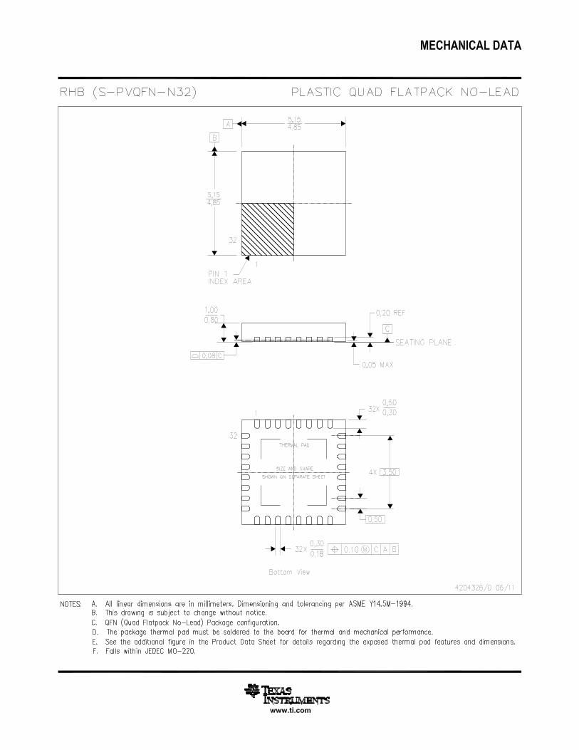
IMPORTANT NOTICE
Texas Instruments Incorporated (TI) reserves the right to make corrections, enhancements, improvements and other changes to itssemiconductor products and services per JESD46, latest issue, and to discontinue any product or service per JESD48, latest issue. Buyersshould obtain the latest relevant information before placing orders and should verify that such information is current and complete.TI’s published terms of sale for semiconductor products (http://www.ti.com/sc/docs/stdterms.htm) apply to the sale of packaged integratedcircuit products that TI has qualified and released to market. Additional terms may apply to the use or sale of other types of TI products andservices.Reproduction of significant portions of TI information in TI data sheets is permissible only if reproduction is without alteration and isaccompanied by all associated warranties, conditions, limitations, and notices. TI is not responsible or liable for such reproduceddocumentation. Information of third parties may be subject to additional restrictions. Resale of TI products or services with statementsdifferent from or beyond the parameters stated by TI for that product or service voids all express and any implied warranties for theassociated TI product or service and is an unfair and deceptive business practice. TI is not responsible or liable for any such statements.Buyers and others who are developing systems that incorporate TI products (collectively, “Designers”) understand and agree that Designersremain responsible for using their independent analysis, evaluation and judgment in designing their applications and that Designers havefull and exclusive responsibility to assure the safety of Designers' applications and compliance of their applications (and of all TI productsused in or for Designers’ applications) with all applicable regulations, laws and other applicable requirements. Designer represents that, withrespect to their applications, Designer has all the necessary expertise to create and implement safeguards that (1) anticipate dangerousconsequences of failures, (2) monitor failures and their consequences, and (3) lessen the likelihood of failures that might cause harm andtake appropriate actions. Designer agrees that prior to using or distributing any applications that include TI products, Designer willthoroughly test such applications and the functionality of such TI products as used in such applications.TI’s provision of technical, application or other design advice, quality characterization, reliability data or other services or information,including, but not limited to, reference designs and materials relating to evaluation modules, (collectively, “TI Resources”) are intended toassist designers who are developing applications that incorporate TI products; by downloading, accessing or using TI Resources in anyway, Designer (individually or, if Designer is acting on behalf of a company, Designer’s company) agrees to use any particular TI Resourcesolely for this purpose and subject to the terms of this Notice.TI’s provision of TI Resources does not expand or otherwise alter TI’s applicable published warranties or warranty disclaimers for TIproducts, and no additional obligations or liabilities arise from TI providing such TI Resources. TI reserves the right to make corrections,enhancements, improvements and other changes to its TI Resources. TI has not conducted any testing other than that specificallydescribed in the published documentation for a particular TI Resource.Designer is authorized to use, copy and modify any individual TI Resource only in connection with the development of applications thatinclude the TI product(s) identified in such TI Resource. NO OTHER LICENSE, EXPRESS OR IMPLIED, BY ESTOPPEL OR OTHERWISETO ANY OTHER TI INTELLECTUAL PROPERTY RIGHT, AND NO LICENSE TO ANY TECHNOLOGY OR INTELLECTUAL PROPERTYRIGHT OF TI OR ANY THIRD PARTY IS GRANTED HEREIN, including but not limited to any patent right, copyright, mask work right, orother intellectual property right relating to any combination, machine, or process in which TI products or services are used. Informationregarding or referencing third-party products or services does not constitute a license to use such products or services, or a warranty orendorsement thereof. Use of TI Resources may require a license from a third party under the patents or other intellectual property of thethird party, or a license from TI under the patents or other intellectual property of TI.TI RESOURCES ARE PROVIDED “AS IS” AND WITH ALL FAULTS. TI DISCLAIMS ALL OTHER WARRANTIES ORREPRESENTATIONS, EXPRESS OR IMPLIED, REGARDING RESOURCES OR USE THEREOF, INCLUDING BUT NOT LIMITED TOACCURACY OR COMPLETENESS, TITLE, ANY EPIDEMIC FAILURE WARRANTY AND ANY IMPLIED WARRANTIES OFMERCHANTABILITY, FITNESS FOR A PARTICULAR PURPOSE, AND NON-INFRINGEMENT OF ANY THIRD PARTY INTELLECTUALPROPERTY RIGHTS. TI SHALL NOT BE LIABLE FOR AND SHALL NOT DEFEND OR INDEMNIFY DESIGNER AGAINST ANY CLAIM,INCLUDING BUT NOT LIMITED TO ANY INFRINGEMENT CLAIM THAT RELATES TO OR IS BASED ON ANY COMBINATION OFPRODUCTS EVEN IF DESCRIBED IN TI RESOURCES OR OTHERWISE. IN NO EVENT SHALL TI BE LIABLE FOR ANY ACTUAL,DIRECT, SPECIAL, COLLATERAL, INDIRECT, PUNITIVE, INCIDENTAL, CONSEQUENTIAL OR EXEMPLARY DAMAGES INCONNECTION WITH OR ARISING OUT OF TI RESOURCES OR USE THEREOF, AND REGARDLESS OF WHETHER TI HAS BEENADVISED OF THE POSSIBILITY OF SUCH DAMAGES.Unless TI has explicitly designated an individual product as meeting the requirements of a particular industry standard (e.g., ISO/TS 16949and ISO 26262), TI is not responsible for any failure to meet such industry standard requirements.Where TI specifically promotes products as facilitating functional safety or as compliant with industry functional safety standards, suchproducts are intended to help enable customers to design and create their own applications that meet applicable functional safety standardsand requirements. Using products in an application does not by itself establish any safety features in the application. Designers mustensure compliance with safety-related requirements and standards applicable to their applications. Designer may not use any TI products inlife-critical medical equipment unless authorized officers of the parties have executed a special contract specifically governing such use.Life-critical medical equipment is medical equipment where failure of such equipment would cause serious bodily injury or death (e.g., lifesupport, pacemakers, defibrillators, heart pumps, neurostimulators, and implantables). Such equipment includes, without limitation, allmedical devices identified by the U.S. Food and Drug Administration as Class III devices and equivalent classifications outside the U.S.TI may expressly designate certain products as completing a particular qualification (e.g., Q100, Military Grade, or Enhanced Product).Designers agree that it has the necessary expertise to select the product with the appropriate qualification designation for their applicationsand that proper product selection is at Designers’ own risk. Designers are solely responsible for compliance with all legal and regulatoryrequirements in connection with such selection.Designer will fully indemnify TI and its representatives against any damages, costs, losses, and/or liabilities arising out of Designer’s non-compliance with the terms and provisions of this Notice.
Mailing Address: Texas Instruments, Post Office Box 655303, Dallas, Texas 75265Copyright © 2017, Texas Instruments Incorporated