Embed Size (px)
Citation preview

AFRL-IF-RS-TR-2000-170 Final Technical Report January 2001
ADVANCED SCALABLE NETWORKING TECHNOLOGY
University of Southern California
Sponsored by Defense Advanced Research Projects Agency DARPA Order No. C929
APPROVED FOR PUBLIC RELEASE; DISTRIBUTION UNLIMITED.
The views and conclusions contained in this document are those of the authors and should not be interpreted as necessarily representing the official policies, either expressed or implied, of the Defense Advanced Research Projects Agency or the U.S. Government.
AIR FORCE RESEARCH LABORATORY INFORMATION DIRECTORATE
ROME RESEARCH SITE ROME, NEW YORK
20010405 107

This report has been reviewed by the Air Force Research Laboratory, Information Directorate, Public Affairs Office (IFOIPA) and is releasable to the National Technical Information Service (NTIS). At NTIS it will be releasable to the general public, including foreign nations.
AFRL-IF-RS-TR-2000-170 has been reviewed and is approved for publication.
APPROVED: ", ,v , - >,
ROBERT L. KAMINSKI Project Engineer
FOR THE DIRECTOR: ' r ' / "^ - "'" J
<T-
WARREN H. DEBANY, Technical Advisor Information Grid Division Information Directorate
If your address has changed or if you wish to be removed from the Air Force Research Laboratory Rome Research Site mailing list, or if the addressee is no longer employed by your organization, please notify AFRL/IFG, 525 Brooks Road, Rome, NY 13441-4505. This will assist us in maintaining a current mailing list.
Do not return copies of this report unless contractual obligations or notices on a specific document require that it be returned.

ADVANCED SCALABLE NETWORKING TECHNOLOGY
John Granacki
Contractor: University of Southern California Contract Number: F30602-95-C-0296 Effective Date of Contract: 01 October 1995 Contract Expiration Date: 30 September 1999 Short Title of Work: Advanced Scalable Networking
Technology Period of Work Covered: Oct 95 - Sep 96
Principal Investigator: John Granacki Phone: (310)822-1511
AFRL Project Engineer: Robert L. Kaminski Phone: (315)330-1865
APPROVED FOR PUBLIC RELEASE; DISTRIBUTION UNLIMITED.
This research was supported by the Defense Advanced Research Projects Agency of the Department of Defense and was monitored by Robert Kaminski, AFRL/IFG, 525 Brooks Road, Rome, NY.
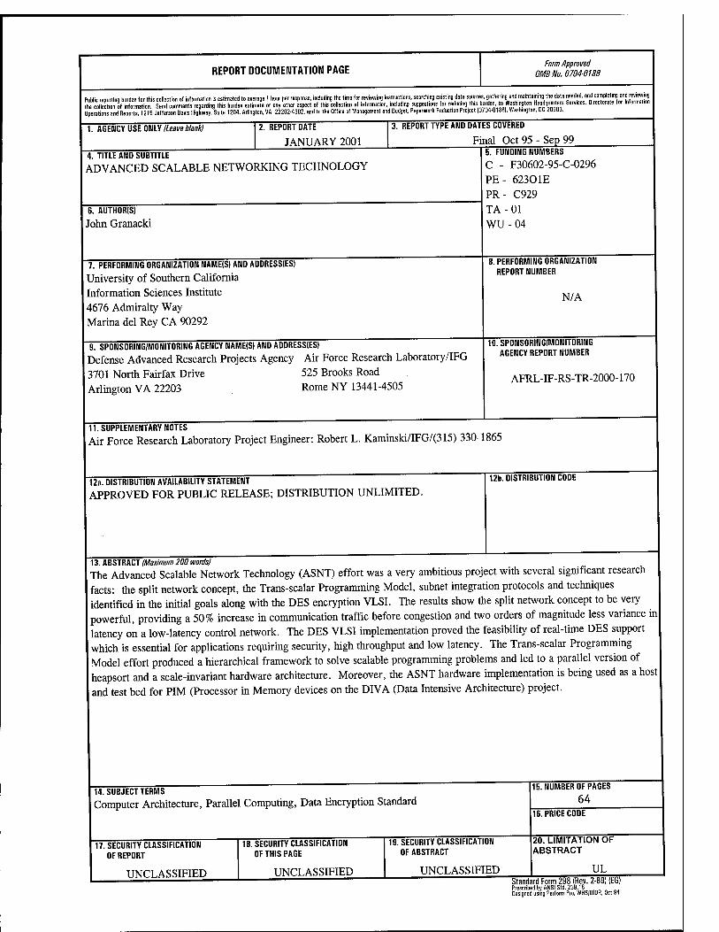
REPORT DOCUMENTATION PAGE Form Approved
OMBNo. 07040188
Public reporting burden for this collection of information is estimated to average 1 hour per response, including the time for renewing instructions, searching »isting data s roes, gathemg and ma am ng no d and comp|e „ ™ «» the collection of information. Send comments regarding this burden estimate or any other aspect of this collection of informa.ron including suggestions tor reducmg this bürdeto Wash^ ton I^eadqua tars Seraces, Directorate for Information
Operations and Reports 1215 Jefferson Davis Highway. Suite 1204, Arlington, VA 22202-4302, and to the Office of Management and Budget, Paperwork Reduction Protect (0704-01881, Washington, DC 20503.
1. AGENCY USE ONLY (Leave blank) REPORT DATE
JANUARY 2001
3. REPORT TYPE AND DATES COVERED
Final Oct 95 - Sep 99 4. TITLE AND SUBTITLE
ADVANCED SCALABLE NETWORKING TECHNOLOGY
6. AUTHOR(S)
John Granacki
7. PERFORMING ORGANIZATION NAME(S) AND ADDRESS(ES)
University of Southern California Information Sciences Institute 4676 Admiralty Way Marina del Rey CA 90292
9. SPONSORING/MONITORING AGENCY NAME(S) AND ADDRESS(ES)
Defense Advanced Research Projects Agency Air Force Research Laboratory/IFG 3701 North Fairfax Drive 525 Brooks Road Arlington VA 22203 Rome NY 13441-4505
5. FUNDING NUMBERS
C - F30602-95-C-0296 PE- 62301E PR- C929 TA- 01 wu -04
. PERFORMING ORGANIZATION
REPORT NUMBER
N/A
10. SPONSORING/MONITORING AGENCY REPORT NUMBER
AFRL-IF-RS-TR-2000-170
11. SUPPLEMENTARY NOTES
Air Force Research Laboratory Project Engineer: Robert L. Kaminski/IFG/(315) 330-1865
12a. DISTRIBUTION AVAILABILITY STATEMENT
APPROVED FOR PUBLIC RELEASE; DISTRIBUTION UNLIMITED. 12b. DISTRIBUTION CODE
13. ABSTRACT (Maximum 200 words)
The Advanced Scalable Network Technology (ASNT) effort was a very ambitious project with several significant research facts: the split network concept, the Trans-scalar Programming Model, subnet integration protocols and techniques identified in the initial goals along with the DES encryption VLSI. The results show the split network concept to be very powerful, providing a 50% increase in communication traffic before congestion and two orders of magnitude less variance in latency on a low-latency control network. The DES VLSI implementation proved the feasibility of real-time DES support which is essential for applications requiring security, high throughput and low latency. The Trans-scalar Programming Model effort produced a hierarchical framework to solve scalable programming problems and led to a parallel version of heapsort and a scale-invariant hardware architecture. Moreover, the ASNT hardware implementation is being used as a host and test bed for PIM (Processor in Memory devices on the DIVA (Data Intensive Architecture) project.
14. SUBJECT TERMS
Computer Architecture, Parallel Computing, Data Encryption Standard
17. SECURITY CLASSIFICATION OF REPORT
UNCLASSIFIED
18. SECURITY CLASSIFICATION OF THIS PAGE
UNCLASSIFIED
19. SECURITY CLASSIFICATION OF ABSTRACT
UNCLASSIFIED
15. NUMBER OF PAGES
64 16. PRICE CODE
20. LIMITATION OF ABSTRACT
UL Standard Form 298 (Rev. 2-89) (EG) Prescribed by ANSI Std. 239.18 Designed using Perform Pro, WHSIDIDR, Oct 94

Table of Contents
1.0 Introduction 1 2.0 Goals and Motivation 1
2.1 Initial Goals 1 2.2 Revised Goals 2
3.0 Results - Theory and Initial Design 3 3.1 Network Simulation 3
3.1.1 MECA Network Simulation, C++ Implementation 3 3.1.2 Network Simulation Graphs 4 3.1.3 Network Functional Specification 7
3.2 SafetyNet 7
3.2.1 SafetyNet Router/Interface Module Design 7 3.2.2 SafetyNet Design Specification 7 3.2.3 SafetyNet Protection Model Tests 8
3.3 DES and the SafetyNet 8 3.3.1 DES Augmentation of SafetyNet 8 3.3.2 SafetyNet Security Subsystem 8
3.4 "Trans-scalar" Programming Model 9 3.4.1 Introduction and Motivation 9 3.4.2 "Trans-scalar" Results H
3.5 Computational Subsystem Architecture (Initial Design) 14 3.6 Software for Parallel I/O Subsystems 17 3.7 Router Size Trade-off Study 20 3.8 PDSS Router Modifications for ASNT 21 3.9 QRAM Protocol for Fast Network Interfaces 22 3.10 I/O Node Subsystem Architecture (Initial Design) 24 3.11 Bridge Node Subsystem Architecture (Initial Design) 25 3.12 Conference Papers Submitted and Accepted 27
3.12.1 "Lessons from Three Generations of Embedded Supercomputers" 27 3.12.2 "Routing in Bidirectional k-ary n-cubes with Red Rover Algorithm" 27 3.12.3 'The Red Rover Algorithm for Deadlock-Free Routing on Bidirectional Rings" - - 27 3.12.4 "A Fully Pipelined, 700 MBytes/s DES Encryption Core" 27
4.0 Results - Design and Implementation 27 4.1 Packaging Architecture 27 4.2 System Chassis 29 4.3 I/O Node Design 32
4.4 Compute Node Design 33 4.5 Bridge Node Details 33 4.6 DES Operational Results 36 4.7 SafetyNet 40
4.8 Router Boards -' 40
4.9 System Clock 40
4.10 System Bootstrap Procedure 41
4.11 Generic Associative Lookup Module 43 4.12 Photo Gallery 45
5.0 Conclusion 47
List of Figures
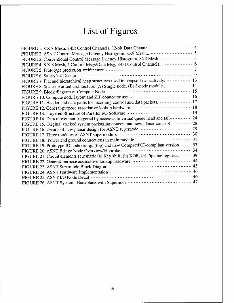
FIGURE 1.8X8 Mesh, 8-bit Control Channels, 32-bit Data Channels 4 FIGURE 2. ASNT Control Message Latency Histogram, 8X8 Mesh... 5 FIGURE 3. Conventional Control Message Latency Histogram, 8X8 Mesh... 5 FIGURE 4. 8 X 8 Mesh, 4 Control Msgs/Data Msg, 8-bit Control Channels... 6 FIGURE 5. Prototype protection architecture. 7 FIGURE 6. SafetyNet Design 9 FIGURE 7. Flat and hierarchical heap structures used in heapsort respectively. 13 FIGURE 8. Scale-invariant architecture. (A) Single node. (B) 8-node module... 14 FIGURE 9. Block diagram of Compute Node 15 FIGURE 10. Compute node layout and ZIF connector use 16 FIGURE 11. Header and data paths for incoming control and data packets. 17 FIGURE 12. General-purpose associative lookup hardware. 18 FIGURE 13. Layered Structure of Parallel I/O Software 19 FIGURE 14. Data movement triggered by accesses to virtual queue head and tail 24 FIGURE 15. Original stacked system packaging concept and new planar concept 28 FIGURE 16. Details of new planar design for ASNT supernode. 29 FIGURE 17. Three modules of ASNT supermodule. 30 FIGURE 18. Power and ground connections in main module. 31 FIGURE 19. Prototype 10 node design (top) and new CompactPCI-compliant version 33 FIGURE 20. ASNT Bridge Node Overview/Floorplan 34 FIGURE 21. Circuit elements schematic (a) Key shift, (b) XOR, (c) Pipeline register... 39 FIGURE 22. General-purpose associative lookup hardware. 44 FIGURE 23. ASNT Supernode Block Diagram 45 FIGURE 24. ASNT Hardware Implementation 46 FIGURE 25. ASNT I/O Node Detail 46 FIGURE 26. ASNT System - Backplane with Supernode 47
in

List of Tables
TABLE 1. 2-Point Switch Router with Conventional Perimeter Pads 20 TABLE 2. 3-Point Switch Router with 2-Tier Pads 21 TABLE 3. Bridge Command Bus Device Map 36 TABLE 4. Function Encodings 36 TABLE 5. Comparison of implementation of one DES round 39
IV

1.0 Introduction The Advanced Scalable Network Technology (ASNT) project builds on our past research experi- ence with scalable multicomputer architectures. The Embedded Variant (EV) project was an i860 based machine, running MACH OS and communicating over a mesh network. The Package- Driven Scalable System (PDSS) was an extremely densely packed, PPC based machine, commu- nicating with custom VLSI 1-D routers. Work on these systems led us to consider the splitting of the communications mechanisms along functional lines, providing optimum service for different types of messaging. This architecture can provide sustained performance much closer to theoreti- cal peak performance than systems with any single conventional network. Also we cast an eye to solving the problems of programmability, software infrastructure, user friendliness and system
balance.
2.0 Goals and Motivation
2.1 Initial Goals The ASNT project will design and deliver a scalable desktop supercomputer. An innovative split network architecture will be developed, and used to provide a scalable system with dramatically improved levels of system balance, programmability and performance. Specific goals of the project are:
• Develop a scalable computer with a communications network divided into four parallel subnetworks:
1. A moderate bandwidth, very low latency network for control messages.
2. A high-bandwidth, moderate latency network for memory-to-memory data transfers.
3. A simple but secure network for communicating and managing protection information.
4. A very-high-bandwidth network, as part of a separate I/O subsystem.
• Develop techniques and protocols for integrating the operation of these subnetworks, to transparently provide higher overall performance to the user.
• Develop and demonstrate a hierarchical programming model which can exploit this improved architecture, to reduce programming effort for complex applications.
Attainment of these goals provides a system platform that:
• enables a new "Trans-scalar" Programming Model" that offers better performance and convenience than either message passing or shared memory.
• provides graceful scalability where hardware and software produce a seamless transition in programming model and performance across node and module boundaries.
• creates an I/O system that is a separate distributed computer linked node to node to the compute system, thus guaranteeing balanced scaling.
• allows a new operating system paradigm in which the distributed operating system is no longer a barrier between the application and the network.
• incorporates SafetyNet, a robust protection network to transparently and efficiently pro- tect users and system from network intrusion or resource misuse.
• supports programming and interface standards, including MPI and MessageWay.
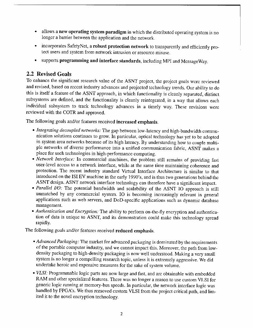
2.2 Revised Goals To enhance the significant research value of the ASNT project, the project goals were reviewed and revised, based on recent industry advances and projected technology trends. Our ability to do this is itself a feature of the ASNT approach, in which functionality is cleanly separated, distinct subsystems are defined, and the functionality is cleanly reintegrated, in a way that allows each individual subsystem to track technology advances in a timely way. These revisions were reviewed with the COTR and approved.
The following goals and/or features received increased emphasis.
• Integrating decoupled networks: The gap between low-latency and high-bandwidth commu- nication solutions continues to grow. In particular, optical technology has yet to be adopted in system area networks because of its high latency. By understanding how to couple multi- ple networks of diverse performance into a unified communication fabric, ASNT makes a place for such technologies in high-performance computing.
• Network Interface: In commercial machines, the problem still remains of providing fast user-level access to a network interface, while at the same time maintaining coherence and protection. The recent industry standard Virtual Interface Architecture is similar to that introduced on the ISIEV machine in the early 1990's, and is thus two generations behind the ASNT design. ASNT network interface technology can therefore have a significant impact.
• Parallel I/O: The potential bandwidth and scalability of the ASNT 10 approach is still unmatched by any commercial system. 10 is becoming increasingly relevant in general applications such as web servers, and DoD-specific applications such as dynamic database management.
• Authentication and Encryption: The ability to perform on-the-fly encryption and authentica- tion of data is unique to ASNT, and its demonstration could make this technology spread rapidly.
The following goals and/or features received reduced emphasis.
• Advanced Packaging: The market for advanced packaging is dominated by the requirements of the portable computer industry, and we cannot impact this. Moreover, the path from low- density packaging to high-density packaging is now well understood. Making a very small system is no longer a compelling research topic, unless it is extremely aggressive. We did undertake heroic and expensive measures for the sake of system volume.
• VLSI: Programmable logic parts are now large and fast, and are obtainable with embedded RAM and other specialized features. There was no longer a reason to use custom VLSI for generic logic running at memory-bus speeds. In particular, the network interface logic was handled by FPGA's. We thus removed custom VLSI from the project critical path, and lim- ited it to the novel encryption technology.

• Router Technology: This was being driven by signalling technology, and specialized pad drivers with GHz speeds were becoming available. We concentrated on the network inter- face rather than building a state-of-the-art router, since the state of the art was changing rap- idly. The network technology is upgradable.
• Programming model: MPI is now a standard on large-scale machines, and is acceptable as a solution on a delivered system. However, the underlying ASNT hardware is capable of much more sophisticated and interesting programming models. We therefore support a good implementation of MPI as the production software, but then focused on providing generic mechanisms with which to build and experiment with innovative programming models, rather than promote any particular new model. We identified and investigated several chal- lenges that needed to be met for practical hierarchical programming. In the end, though solvable in a hierarchical fashion, a fully implemented solution was beyond the scope of the proposal.
Revisions to the technical plan were as follows:
1. All network interface functionality was moved off the Compute and IO Nodes, and onto the Bridge Node, where access is tightly controlled for protection and management reasons. This had following consequences: • The Bridge Node is the most complex part of the system. • The Compute and IO nodes each export their 60X system bus through a connector. • The Compute and IO subsystems no longer form stand-alone distributed systems. Instead,
Compute and IO nodes plug into the Bridge Subsystem, which provide each type of node with direct access to its associated IO or Command/Data network.
2. IO Nodes and Compute Nodes have the same physical interface to the Bridge Node, so IO Node boards can be used as Compute Nodes.
3. The form factor of the delivered system is larger than originally estimated, although still desktop sized. However, it is amenable to aggressive application of laptop technology, which would shrink the dimensions well below the original estimate.
3.0 Results - Theory and Initial Design
3.1 Network Simulation
3.1.1 MECA Network Simulation, C++ Implementation
The MECA Network Simulator was reimplemented in C++ to allow convenient use for hierarchi- cal network simulations. Validation tests were run comparing it with the original C version, and with real hardware. Both versions reproduce the actual hardware performance. However, at high traffic rates there is a slight numerical discrepancy between the C and C++ versions, which was traced to an implicit design ambiguity in the arbitration between simultaneous events.

3.1.2 Network Simulation Graphs To develop a functional specification for the control and data nets of ASNT, we conducted numer- ous simulation experiments, such as the following. The message activity on the network is mod- eled as one in which nodes perform remote reads by requesting data from other nodes at a Poisson rate. This data transfer consists of 2 steps:
1. The source sends a 40-byte control message to a destination to request data.
2. In response to the request, the destination sends a 4-kbyte data message to the source.
The simulator allows several input parameters: network topology, traffic rate, network organiza- tion (ASNT or conventional), etc. If a conventional network organization is chosen, both control and data messages share the same set of channels. However, for the ASNT organization, the chan- nel wires are allocated so that control messages have sole use of one set of channels while data messages use another set.
For all experiments, the simulator was run with random destination traffic patterns. The results presented are the averages of several runs. For each run, statistics gathering is initiated only after warm-up transient effects become negligible. Results for average head-to-tail message latency versus traffic load on an 8 X 8 mesh are shown in Figure 1.
12000
V)
ü
,0,
>, ü c CD
CD CO co </> w CD
CD CD CO
CD > <
10000
8000
6000
4000
2000
ASNT, control -e- conventional, control -+-
ASNT, data -*- conventional, data ■■•*•■■
!>:::::
-dr-v
60 120 180 Request Rate Per Node (requests/million cycles)
240
FIGURE 1. 8 X 8 Mesh, 8-bit Control Channels, 32-bit Data Channels
Head-to-tail message latency is defined as the amount of time from the generation of a message until the tail flit of the message is received at the destination. Below, "conventional case" refers specifically to a network organization in which both control and data messages share the same set of 40-bit channels. Several other cases with varying network topologies, message sizes, etc., were simulated, and all yielded similar results. For brevity, we present only the 8 X 8 mesh cases.Notice that for the ASNT organization with separate control and data networks, the latency

for control messages is fairly constant and therefore predictable. For the conventional organiza- tion, the control message latency increases with the data message latency as expected, since the two message types share the same channels. However, by comparing the sum of the ASNT curves to that of the conventional curves, we see that simply partitioning the network offers little
30
CO <D O) CO CO CO CD
CD en CO
c CD Ü L_
CD
25
20
15
10
_i i 11 i ii i ii
0 10 20 30 40 50 60 70 80 90 Message Latency (cycles)
FIGURE 2. ASNT Control Message Latency Histogram, 8X8 Mesh, 130 requests/million cycles
CO CD O) CO CO CO CD
o CD O) CO
+-< c CD Ü CD
0 1000 2000 3000 4000 5000 6000 7000 8000 9000 10000 Message Latency (cycles)
FIGURE 3. Conventional Control Message Latency Histogram, 8X8 Mesh, 130 requests/million cycles

improvement in the overall latency of the remote read operation. However, considerable improve- ment can result from optimizing the control and data networks for their specialized functions.
Even without such specialization, a major contribution of ASNT is the provision of a predictable low-latency control network. To confirm the predictability of the ASNT control network, histo- grams of control message latency are shown in Figure 2 and Figure 3. The variance in control message latency in the ASNT case is seen to be two orders of magnitude less than in the conven- tional case.
Since the major benefit of ASNT in these cases is the guaranteed low latency of control messages, it is useful to determine the amount of traffic the control network can sustain and still perform this well. We are currently conducting experiments to ascertain this point. Preliminary data is given in Figure 4. The message traffic for this case is a Poisson distribution of control messages where 25% of the control messages are remote read requests and require a response of a data message, as described earlier. The remaining control messages represent generic short system messages which require no response. As shown in the graph, the ASNT system can easily sustain the extra traffic on the control network. However, the congestion of the conventional system is exacerbated by the extra traffic, causing it to saturate at a significantly lower traffic rate, as indicated by the vertical asymptotes of the curves. For this case then, ASNT not only provides a low-latency con- trol network, it also provides higher system throughput.
CO O O
>> O c CD
CD U) CO CO CO CD
CD O) CO 1_
CD > <
10000
9000
8000
7000
6000
5000
4000
3000
2000
1000
0
1 1 X □
/+
ASNT, control -*— /;
/ conventional, control --<—- :'i' ;'
ASNT, data •«•- 11 conventional, data •-•* 1! -
- .D
-
,x/- ..a
. ..-□''" ' ■Q;:; * ,i
□ x ,- >■ x -X-
y -
+"' «___ --*- -~?» 1 A Ä U_«
0 300 600 900 Control Message Injection Rate Per Node (requests/million cycles)
FIGURE 4. 8 X 8 Mesh, 4 Control Msgs/Data Msg, 8-bit Control Channels, 32-bit Data Channels

3.1.3 Network Functional Specification A more comprehensive design specification document is available on request. The most unique points are included in Section 3.6 Computational Subsystem Architecture, second half and 4.11 Generic Associative Lookup Module.
3.2 SafetyNet
3.2.1 SafetyNet Router/Interface Module Design To assess the real hardware overhead from enforcing protection, an architecture for a SafetyNet module was developed for inclusion in the router/interface component on the PDSS project. The module inserts and check protection bits in each message and enables safe direct user access to the communication hardware (Figure 5). This is not a complete implementation of the SafetyNet concept since the protection information is not carried on a separate protected network, and the system as a whole is still vulnerable if the user penetrates the OS protection on any one node. However, it will allow measurement of the silicon area and number of clock cycles required by the logic interfacing to the control, data and I/O networks.
Register number or physical DRAM address
Incoming Packet
/
yf- Sending Principal Identifier (N bits)
FIGURE 5. Prototype protection architecture.
Receiving Principal Identifier (N bits)
Processor and Interface registers
Access to processor or interface registers requires exact match between ID of message sender and ID of current user of the processor.
DRAM
Valid Principal Mask (2N bits)
Access to DRAM only requires mask bit corresponding to sender's ID to be equal to 1, allowing several prin- cipals to validly access DRAM.
3.2.2 SafetyNet Design Specification A more comprehensive design specification document is available on request. The most unique points of the design have, however, been included in this final report.

3.2.3 SafetyNet Protection Model Tests For test purposes, a prototype of the SafetyNet network filter was included in the RIF network chip, a component developed for the PDSS project. The filter supports a communications inter- face in which applications have direct access to local and remote network hardware, by stamping outgoing packets with an identifier, and allowing receiving nodes to selectively intercept packets when necessary.
The filter logic was tested successfully, and operated as designed. Extensive testing was not pos- sible in this iteration of the chip because unrelated problems in the ground circuitry of some on- chip data buffers precluded processing large volumes of network traffic.
3.3 DES and the SafetyNet
3.3.1 DES Augmentation of SafetyNet A survey of security and cryptographic literature was conducted to establish a starting point for the architecture of the SafetyNet security subsystem. As a result of this survey, we have elected to augment the initial protection mechanisms of the SafetyNet, i.e., network-interface firewalls, with encryption and cryptographic authentication of the data resident in the I/O node memory and transported by the I/O network. The XOR message-authentication code (XOR MAC) technique recently developed at IBM is amenable to parallel and pipelined implementations. This is in marked contrast to other cryptographically strong MACs in current use, such as MD5 or cipher- block-chained DES. Present network cryptographic MAC techniques were developed for efficient software implementation, and are severely limited in their ultimate performance by inter-block chaining, which introduces dependencies that preclude substantial pipelining or parallelism in implementations.
In support of the specification of the high-bandwidth encrypting bus bridge component of the SafetyNet, sample encryption circuitry was specified in the Epoch VLSI synthesis system to pro- vide chip area and timing estimates for a pipelined encryption implementation. As a result, we estimated that the bridge, with the three DES computational pipelines required for simultaneous data encryption and XOR MAC authentication, can process data at rates in excess of 400MB/s with a chip area comparable to that of our PDSS router and network-interface design (roughly 250,000 transistors). If realized, this throughput would be an order of magnitude superior to exist- ing provably-hard cryptographic authentication systems.
3.3.2 SafetyNet Security Subsystem We have chosen to incorporate our high-performance encryption and authentication technology in an encrypting bus bridge between a "Siamesed" pairing of the computational and I/O nodes (see Figure 6). Data will be encapsulated in "secure objects" which will be encrypted and tagged with cryptographic authentication codes on the fly as they are transmitted at full bus speeds between the two nodes. This new bus bridge component of the SafetyNet security subsystem is more highly coupled with the I/O node than originally envisioned, so some parts of the I/O node design, primarily the memory system interface, were reworked as needed.

Compute Node Encrypting Bridge > 400 MB/s
I/O Node
64MB DRAM DIMMs
333MHz PowerPC
604e
64b
+-H>
Pipelined DES ECB
Calculator
Pipelined DES XOR MAC Calculator
SafetyNet-<-
I
64b
<"/-►
64MB DRAM DIMMs
266MHz PowerPC
603e
33MHz PowerPC
860EN ->> SafetyNet
FIGURE 6. SafetyNet Design
The initial version of the SafetyNet was implemented using Altera FlexlOK FPGA programmable logic under the control of an embedded processor which performs initialization and key manage- ment. The complexity of the encryption and authentication datapaths was too great for compact implementation in the FPGAs, so we initially implemented a reduced number of the 16-stage DES pipelines. We also elected this course in VLSI implementations. This validates our control- logic and datapath designs and timing estimates at lower cost than the fully replicated 16-stage final product. Some parameters of the detailed design therefore reflect the results of fitting HDL- synthesized logic into the FPGAs.
3.4 "Trans-scalar" Programming Model
3.4.1 Introduction and Motivation The basic insights motivating this hierarchical programming model are as follows.
1 The main challenge in programming distributed-memory machines is managing data move- ment and synchronization. The message-passing paradigm is inconvenient because it splits each data movement into two operations, a send and a receive. Similarly, a shared memory model supporting remote read and write introduces synchronization complexities. Both of these can be avoided in a small machine by having a centralized controller manage data move- ment, synchronization, and computation scheduling.
2. The centralized controller can be realized as a von Neuman CPU. Data movement then appears as load and store operations of data blocks, execution of a task appears as dispatching a block instruction, and synchronization is implicit, because loads, stores and block operations are con- ceptually atomic.
3. Similarly, in a large machine, several centralized controllers, each managing a portion of the system, can in turn be managed by a master controller. Data objects maintained by the master controller are directories listing objects managed by the local controllers. Instructions per-

formed by the master controller manipulate directories and perform operations on the pointers that are their contents. The layering can be repeated to create a hierarchy of controllers, con- trolling as large a system as desired with only logarithmic overhead.
4. Programming complex applications in this model should be more convenient than either the single program or multiple process models available now, because the programmer has both a global and a local view of the machine, depending on whether one is programming a controller or one of the nodes it manages. It should also be more flexible, since the data structures used to manage distributed data are directly accessible to the application as higher-level objects. Thus, one should be able to successfully program applications involving very complex data move- ments and synchronization patterns.
5. On the ASNT system, very efficient control-message transactions can facilitate managing com- putations in much more sophisticated ways than on current machines. In particular, a controller node can maintain close control over its subordinates, and not adversely impact their through- put with context switches, high-cost interrupts, etc.
The challenge is to turn these insights into a complete, general-purpose programming model. A literature search was performed to locate prior work along these lines, and the conclusions were:
1 There are numerous existing models based on the divide-and-conquer paradigm, which is applicable to restricted classes of algorithm. However, these do not address data movement, or simplify it in any way. Also, they do not exploit the fact that there is an isomorphism between the machine acting as a controller and the machine being controlled. Instead, they work explic- itly with groups of processors. The most extensive work of this type is by the "Skeletal Paral- lelism" group, e.g. Skeleton-based Parallelisation of Functional Programs, Bratvold 1995 and Towards a Skelton Based Parallelising Compiler for SML, Michealson, Ireland &King 1997 at Heriot-Watt University, Edinburgh, UK.
2. The divide-and-conquer approach is generally regarded as simply one of a number of classes of algorithm needed for parallel programming. There is no analog of our observation that the other classes of algorithm, e.g., systolic, SIMD or dataflow, are also special cases of a more generally applicable hierarchical model of distributed computation.
3. Many authors have remarked that good scalable algorithms seem to be hierarchical, but have not pursued any practical implications of this fact.
4. Ad hoc hierarchical approaches were common in the days of hypercubes, but have waned since then, under the misperception that mesh topologies do not need them or support them well.
We identified several challenges that need to be met to make the hierarchical programming approach practically useful. We investigated these by developing a C-based package for imple- menting hierarchical applications. It appeared that each of these challenges amounted to solving a major problem with existing scalable programming techniques, and that the hierarchical approach provides a uniform and consistent framework for solving them.
1. Data objects must be relocatable. For the system to move data blocks around in response to load and store operations from a controller, these data blocks must be relocatable. The use of pointers in data must thus be carefully restricted. On the other hand, directories make heavy use of pointers, and directories are simply data blocks to a higher-level controller. We resolve
10

this dilemma by observing that a controller and a controllee operate in different name spaces. The controllee has access to a few data blocks, and can access their contents, whereas the con- troller has access to many more data blocks, but cannot access their contents. As long as con- troller and controllee use pointers within their own name spaces, data remains relocatable, without requiring a non-scalable global address space. This approach appears able to resolve the contentious issue in scalable computing of how to provide a global address space, and whether it should be physical or virtual.
2. Inconvenient boundaries must be removed. Existing hierarchical approaches are tree-based, and trees have the undesirable property that they introduce artificial logical boundaries between nodes. Thus, two nodes may be physically adjacent, but if they are located in different coarse-grained subtrees, significant administrative overhead can be required to allow them interact. A resolution is to organize the hierarchy so that controller domains overlap, and phys- ically adjacent nodes are guaranteed to both be members of at least one such domain. This introduces an aliasing and synchronization complication, but it is one that can be handled transparently by the system.
3. Copy vs. move semantics. In conventional programming, loads and stores are copy operations between source and destination, and for large distributed objects this can waste resources if the desired operation is actually a move. It is also slow if source and destination are on the same node, and the move can be accomplished by simply renaming the object. Lazy copying supple- mented with copy-on-write techniques can solve this partially, but they can nullify attempts at latency hiding. Thus, the controller operations, and the language or compiler used for program- ming them, need to distinguish between copy operations and move operations.
4. Type strictness issues. Directory entries, which make up the data of higher-level objects, can be implemented with a range of type strictness. Least strict is to treat them as ordinary data. Alter- natively, all directory entries could have one special type. Finally, a directory entry could have a type specific to the type of the object it refers to, and/or the type of object it is present in. It is not resolved at present how type information is best distributed between the compiler, the application, and the system. We are investigating whether the typing available in C is strong enough to conveniently implement a large hierarchical system.
5. Control dependence issues. A distributed computation cannot proceed efficiently if the direc- tions of branches in one part of the machine often depend on highly dynamic data in another remote part of the machine. Whatever the application, developing a successful scalable appli- cation hinges on solving this issue in one way or another. In our case, the issue appears very cleanly and explicitly: branches in the program executing on a controller node should not depend regularly on the details of the contents of the objects it is managing. This caveat leads to a useful principle for structuring scalable algorithms.
3.4.2 "Trans-scalar" Results
The Trans-scalar Programming Model proved to be a concept with far-reaching applications, but is subtle and requires extensive work. The assessment was made that the specification of a com- plete, implementable hierarchical programming model along these lines was beyond the scope of the contract. This did not affect the ASNT system itself, which can support conventional program- ming models, including MPI, as planned.
11

Nevertheless, a number of promising results using the Trans-scalar Model have been achieved. We discuss two of these results here.
First, use of the Trans-scalar framework has led to the discovery of a parallel version of the heapsort algorithm. Although not quite as fast in the average case as quicksort, heapsort is a very powerful and popular algorithm because it has the same N log N complexity as quicksort for the average case, and its worst case complexity is also N log N. In contrast, the worst-case complexity of quicksort is N . There are numerous parallel sorting algorithms available in the literature, including quicksort, but heapsort has eluded parallelization until now because its complicated data movement requirements have been too difficult to analyze and implement on a distributed memory machine.
The basic idea of sequential heapsort is to consider the items to be arranged as a binary tree, and then migrate large items towards the root and small items towards the leaves. It takes log N steps for the largest item to reach the root of the tree, where it can be removed and placed at the end of an ordered list.
It might seem that this treelike heap structure is artificially well-suited to a hierarchical program- ming model, and therefore not a good illustrative example. However, just the reverse is true. The hierarchical structure exposed by the Trans-scalar paradigm is unrelated to the heap structure, and is easily applied to other sorting algorithm as well. An intuitive derivation of the algorithm is as follows.
Consider sorting a large set of N items. Suppose that, accidentally, groups of M adjacent items in the unsorted set are identical, i.e., that the set consists of N/M blocks, each of which contains M copies of one item. Clearly, if one knew ahead of time that the set had this structure, it could be sorted much faster than the theoretical average N log N, by just treating each block as a unit and sorting the blocks.
One can therefore write a heapsort routine for the blocks, which is identical to the one from Press et al's Numerical Recipes, except that 1) Each numerical comparison is replaced by a "block com- parison" routine that compares a representative item from each blocks, and 2) Each data exchange becomes a block data exchange.
Next, suppose that the items in each block are not necessarily identical, but that the ranges of val- ues in separate blocks do not overlap. Then one can still use the above algorithm, provided 1) the comparison uses maximum and minimum values from each block, and 2) there is an additional step to sort the contents of each block. This is still faster than sorting all N items together. More- over, it is parallelizable, because the sorting of individual blocks can be done concurrently.
Finally, consider the completely general case where there is no known relationship between items in different blocks. One can still use this algorithm, provided each comparison operation is replaced with a "merge and compare," in which two blocks of items are sorted into two new blocks containing the largest and smallest items. The fact that individual blocks can be sorted in parallel is still true. Moreover, one can use heapsort to sort block contents, or if blocks are large, one can split each block into sub-blocks, and reapply the algorithm we have just presented.
12

Flat
Hierarchical
FIGURE 7. Flat and hierarchical heap structures used in sequential and hierarchical heapsort respectively. The hierarchical grouping essentially identifies blocks that can be usefully sorted concurrently.
We programmed this hierarchical algorithm and tested it with random data sets of up to 1 million items on a Sparestation. It is some 30% slower than an optimized sequential quicksort, and about 10% slower than a sequential heapsort. In return for this, it is in principle automatically parallel- izable within the Trans-scalar framework, which is designed to treat blocks of data as individual objects. Figure 7. shows the heap structure in a conventional sequential heapsort, and two levels of the heap structure in a hierarchical heapsort where each block contains 3 items.
We began design of a class library for C++, essentially creating a C++ language extension we call preC. This allowed construction of hierarchical programs exhibiting several key features abstracted from examples such as the one above. The name derives from the fact that each object (i.e., block of items in this example) is conveniently summarized by a smaller object (in this case the maximum and minimum values of the range), and that only the information in the summary is required globally for the computation to proceed. This appears to be one of the common features of scalable algorithms.
The second result is a scalable hardware architecture which illustrates several of the useful properties of self-similar hierarchical systems, in particular the ability to achieve graceful scaling across node and cabinet boundaries. The architecture was not being proposed for implementation under ASNT, but is intended to facilitate analysis of the Trans-scalar Model. Consider building a two-dimensional scalable system as follows.
The basic building block is the node shown in Figure 8, which is a rectangular module containing a network router, some onboard computational components (not shown) and connectors on two edges. Eight of these modules are arranged in a one-dimensional network, using an extra board for the top and bottom of the eight-node system. The top board provides a connection to a higher-
13

E (A)
FIGURE 8. Scale-invariant architecture. (A) Single node. (B) 8-node module. (C) 8 -node 3rd-order module.
(C)
bandwidth network, and the bottom board provides edge connections for the original one-dimen- sional network. Now the 8-node module is simply a scaled-up version of the node, so it can be used to build a larger system, etc. At each step, one combines 8 modules and adds hardware for a higher-bandwidth network, to create a similar module.
The system is clearly scalable. However, it is different from conventional scalable systems in that it has no intrinsic scale, i.e., it is scale-invariant, not just scalable. The computational components on the original node could similarly be a scaled down version of the figure.
The network is also interesting in that there are no module boundaries: every node is connected to it's neighbors by fine-grained network links. The higher bandwidth links form express channels between modules, and the one-dimensional network is wound into a space-filling curve. Three- dimensional analogs exist as well.
Some of the practical aspects of this design were borrowed to create a high-density packaging- driven scalable system under the Integrated Thermal Management (ITEM) project at ISI
3.5 Computational Subsystem Architecture (Initial Design)
A node in the computational subsystem consists of the ControlNet and DataNet hardware, a high-performance microprocessor for doing the bulk of the computation in an application, a high- speed memory system, and an interface to the SafetyNet and I/O subsystems. Figure 9. is an ini- tial block diagram, and Figure 10. shows an initial board layout.
The cache and network logic were designed on a separate daughter board for maximum flexibility. Attachment to the nodeboard is through a 288-pin ZIF socket, which had recently become avail-
14

FIGURE 9. Block diagram of Compute Node
60S CT
60X 60X ^ ADDR DATA
603e MPC106 or PAL
+J t Sr 'S
Dat
al
CtlN
z
R/W
▲ A C 1 A4 £ L
1 IT 1
Integrated Network Interface and L2 Cache
_
t XX XX XX able, and which Motorola was using in their own PowerPC systems. Because of its convenience, this socket was also to be used as a general attachment technique in the ASNT system, for con- necting Compute, SafetyNet and I/O subsystems. Signals were to be brought out as pin arrays on one board, and inserted into the ZIF socket of another board.
The final ASNT system (late '98) would use PowerPC 604 processors. For the Early ASNT pro- totype we use 200MHz PowerPC 603 processors, which, although not as fast at floating point, are pin-compatible with the 604 and much cheaper ($211 each).
We have investigated using the Motorola MPC106 PowerPC system integration component for the glue logic on the Compute node. The MPC106 contains all the necessary bus-, memory- and cache-control logic required for a PowerPC system, on one configurable chip, as well as a large amount of other logic such as a PCI bus interface. However, the cache model is inadequate for our fast network interface, and would have to be bypassed, so the only module the compute system would use from the 106 would be the Synchronous DRAM controller. We are therefore planning to replace the 106 on the compute node with simpler PALs. The 106 remains an integral part of the I/O node design, where the cache model is adequate and the PCI interface will be exploited.
The fast network interface uses a technique called snarfing to minimize the amount of bus activ- ity required to send and receive packets. Packets arriving from the network are held in the network interface, where they are tagged with the RAM address they will ultimately be written to. If the microprocessor reads this address, the network interface responds instead of the DRAM, and puts the data on the bus just as a normal cache would. However, unlike a typical cache, the network interface simultaneously converts the intercepted DRAM read into a DRAM write, so that the data is inputted by the microprocessor and stored into DRAM simultaneously. The data in the interface is thus effectively flushed to DRAM, so the interface can invalidate the block it is holding, and make way for the next arriving packet.
Using this technique means that every arriving packet appears only once on the data bus, com- pared to a normal delivery which drives it once to write to DRAM, and once when the micropro-
15

cessor reads it from DRAM. It is therefore the fastest possible way to deliver network packets without introducing multiple buses.
Long data messages are delivered using a slight variation of this policy: the head of the message is cached in the interface for a fixed number of cycles, to allow the microprocessor time to come in and read it. If the microprocessor continues to read the message sequentially, all data is obtained directly from the interface. However, if the data is not read by the microprocessor within the specified number of cycles, the interface proceeds to flush the data to DRAM so that the long message does not continue to block the network.
The network interface on the send side is similar, and includes a mechanism for triggering the sending of data.
Transparent integration of the control and data networks is achieved as follows. For highest per- formance transfers of large amounts of data, the best algorithm is to send header information to the destination on the ControlNet, so that it arrives well ahead of the data, and the receiving node has time to prepare for receiving data. This preparation can include fetching partial cache lines requiring read/modify/write, configuring the inline shifter to align incoming data properly, notify- ing a user process that data is about to arrive, etc.
To avoid the situation where congestion or failure on ControlNet causes the header information to arrive after the data, we use a protocol where a copy of the header information is automatically sent as part of the data message as well. If the control message arrives first, it is used to begin reception setup, but if it is delayed, reception can still proceed using the copy included with the data, and the message can be drained from the DataNet hardware.
The control message is thus a performance hint to the receiving side. The interface architecture is such that headers on the Control- and DataNets follow the same logic path once they are identified as headers. (Figure 11.). The headers are tagged with unique identifiers, so that the interface can match data to the correct header when multiple messages are processed simultaneously.
16MB DIMM's 288 Pin ZIF Socket
PGA on Bottom for Bridge Node Connection
FIGURE 10. Comput e node layout and ZIF connector use
ZIF Socket for Daughter Card
16

OTHER CTL PACKETS <
RCV HINTS
HDR
BODY ri'<
TAG LOOKUP MODULE
TAG RCV DESC
DATA SHIFTER
a
ADDR
DATA
FIGURE 11. Header and data paths for incoming control and data packets.
The value of a multistage implementation strategy is clearly illustrated in the design of the associative lookup module, the hardware required for tag matching. Similar modules are used in other places in the interface, e.g., for converting node numbers to routing information. The aver- age speed of the lookup depends on the size of the table maintained within the module, and the statistics of the incoming lookup requests. Performance and flexibility of the lookup thus depends directly on the implementation effort. To facilitate early system integration and testing, associa- tive lookup modules was to be implemented in the following steps (see Figure 12).
1 Header information is maintained in DRAM by the CPU, and is passed to and requested from the CPU on each transaction., using CPU-accessible registers in the interface plus interrupts.
2. An internal "active header register" is added to store the header information and tag of the most recently received header. The tag on an arriving data message is compared against the tag of the active header register, and if it matches, the header information is used immediately, with- out requiring intervention from the CPU. If the match fails, the CPU is interrupted, and it stores the active header in DRAM and replaces it with the matching one.
3. A cache is added to hold several recently received headers, so that if the tag misses in the active register, the cache is checked before interrupting the CPU.
4. A hash table state machine and a table base register are added, to support searching a DRAM hash table for headers if the tag misses in the cache, without interrupting the CPU. If the header is not present in the hash table, the CPU is interrupted.
The same mechanism can be used for associative lookup of any type of information, not just head- ers. It is analogous to the TLB support for virtual address translation within the CPU. This approach yields an extremely flexible network interface, with efficient separation of mechanism and policy for data transfers.
3.6 Software for Parallel I/O Subsystems We surveyed available parallel I/O software, and designed a system. The system is layered as shown in Figure 13.
17

The functions of the layers are as follows:
1 The disks are off-the-shelf 2GB UltraSCSI disks suitable for use in Apple Macintosh systems. SCSI disks have built-in interface electronics which allows a controller to interact with the disk using a standard set of commands, and reference data blocks on the disk using logical block numbers rather than cylinder, head and sector information.
2. The controller is also a COTS UltraSCSI board, currently anticipated to be an Adaptec AAA- 130 series. These boards can support either a single drive, or multiple drives configured trans- parently as a RAID subsystem. In either case, the interface to the Operating System is a stan- dard PCI Bus Master protocol, and the data on the disks is accessed using logical block addresses. Redundancy is managed transparently by the board itself.
3. The disks managed by each disk controller are treated as a single Linux file system. Linux already contains drivers support for Adaptec Boards, although small modifications will be required to support the 130-series.
4. The function of the parallel file system is to integrate the separate Linux file systems into a sin- gle system, with a single name space, and with data from each file distributed across several nodes. The parallel file system differs from a conventional sequential file system in that it can efficiently support concurrent access to the same file from many nodes. It can also maximize transfer rate by operating all disk channels concurrently.
NOT-PRESENT INTERRUPT, to CPU
HASH- TABLE ENGINE
Off-chip hash table in DRAM
On- or off-chip hash- table engine
Iqvir continue default abort wait
CACHE CTLR
B : K C Q
u, * < §4- * es u
<—JTAGI I VAUTE REG~I ►
-JlÄfil I ACTIVE ~~l ►
-*A nF.FAt;T7r~r-
CPU accessible registers
Recent values in cache
Active value in register
TAG VALUE
FIGURE 12. General-purpose associative lookup hardware.
18

FIGURE 13. Layered Structure of Parallel I/O Software
i i
Concurrent Process
Concurrent Process
Parallel I/O System
Concurrent Process Compute
Subsystem
Parallel File System
Linux File System
Linux File System
Linux File System Device (I/O)
Subsystem
UltraSCSI Disk Controller
UltraSCSI RAID Disk Controller
UltraSCSI Disk Controller
SuperNode A SuperNode B SuperNode C
ASNT will use the Portable Parallel File System (PPFS), which is a library of I/O routines from the University of Illinois (UIUC) implemented on top of a set of conventional Unix file systems.
5. The Parallel I/O System is another layer of library routines which application processes use to perform file I/O. Its primary goal is to provide a standard, portable interface between the I/O system and the application. The usual Unix open/seek/read/write/close primitives are inade- quate because they involve an implicit shared file offset pointer, and thus force sequential access semantics on the I/O. ASNT is using the MPI-IO standard as an interface, because it addresses this in a simple way, and it is likely to be part of the next MPI standard.
6. The concurrent processes run on the compute nodes, and perform I/O using the MPI-IO primi- tives. These are conveyed via the SafetyNet bridge nodes to the parallel file system on the I/O nodes.
Several alternative parallel file systems were investigated, including IBM's commercial PIOFS and its research version Vesta, Intel's PFS, the Galley Parallel File System from Dartmouth, the Scotch Parallel Storage System from CMU, the PASSION system from Syracuse, the Wisconsin SHORE system, and HiDIOS, a file system for a Fujitsu array processor.
19
PPFS was chosen because it is well tested, and is implemented at the library level, allowing con- venient modification and debugging. It is compatible with the ASNT secure objects model, essen- tial providing a high-level naming and retrieval model for the ASNT secure objects stored on disk.
The ASNT I/O system may be enhanced by supporting a second level of redundancy, between file systems on distinct nodes. This can be achieved by running CMU's RAIDframe software as a layer between the parallel file system and the individual Linux file systems. For very large sys- tems this would provide a extra measure of fault tolerance, for instance against failure of the disk controllers themselves. However, for the ASNT prototype, supporting RAID at each node sepa- rately was the primary goal.
To create a development system, we have installed Linux on two PowerPC-based Macintosh clones connected via fast ethernet. The PPFS and MPI-IO software was installed
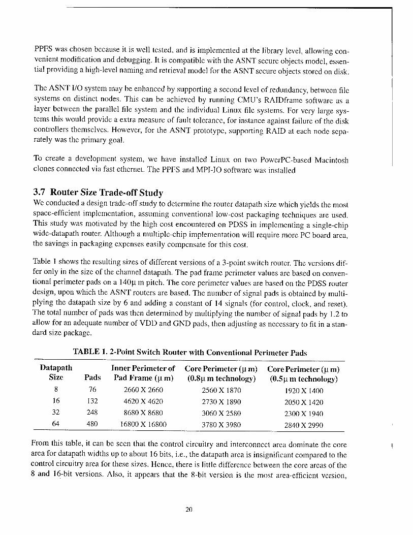
3.7 Router Size Trade-off Study We conducted a design trade-off study to determine the router datapath size which yields the most space-efficient implementation, assuming conventional low-cost packaging techniques are used. This study was motivated by the high cost encountered on PDSS in implementing a single-chip wide-datapath router. Although a multiple-chip implementation will require more PC board area, the savings in packaging expenses easily compensate for this cost.
Table 1 shows the resulting sizes of different versions of a 3-point switch router. The versions dif- fer only in the size of the channel datapath. The pad frame perimeter values are based on conven- tional perimeter pads on a 140u.m pitch. The core perimeter values are based on the PDSS router design, upon which the ASNT routers are based. The number of signal pads is obtained by multi- plying the datapath size by 6 and adding a constant of 14 signals (for control, clock, and reset). The total number of pads was then determined by multiplying the number of signal pads by 1.2 to allow for an adequate number of VDD and GND pads, then adjusting as necessary to fit in a stan- dard size package.
TABLE 1. 2-Point Switch Router with Conventional Perimeter Pads
Datapath Inner Perimeter of Core Perimeter (u.m) Core Perimeter (|im) Size Pads Pad Frame (|im) (0.8 ^tm technology) (0.5 ^im technology)
8 76 2660 X 2660 2560 X 1870 1920 X 1400
16 132 4620X4620 2730X1890 2050X1420
32 248 8680X8680 3060X2580 2300X1940
64 480 16800X16800 3780X3980 2840X2990
From this table, it can be seen that the control circuitry and interconnect area dominate the core area for datapath widths up to about 16 bits, i.e., the datapath area is insignificant compared to the control circuitry area for these sizes. Hence, there is little difference between the core areas of the 8 and 16-bit versions. Also, it appears that the 8-bit version is the most area-efficient version,
20

regardless of technology, although in the 0.8 |im version the space between the core and pad frame may not be adequate for interconnect routing. The 16-bit version is the next best option. The main benefit of using the 16-bit version over the 8-bit version is that chip count is reduced by 50% when constructing larger datapaths. It is also clear from the table that, with peripheral pads, 32-bit and 64-bit versions are not practical due to large amounts of wasted space.
MOSIS does support 2-tier pads at a slightly larger pad pitch within a tier. For 2-tier bonding, smaller pad frames result, as shown in Table 2. In this case, an 8-bit version would require the
TABLE 2.3-Point Switch Router with 2-Tier Pads
Datapath Size Pads
Inner Perimeter of Pad Frame (p. m)
Core Perimeter (|i m) (0.8 (i m technology)
Core Perimeter (|i m) (0.5 u.m technology)
8 76 1750X1750 2560X1870 1920X1400
16 132 2800 X 2800 2730X1890 2050 X 1420
32 248 5430 X 5430 3060 X 2580 2300 X 1940
64 480 10500 X 10500 3780 X 3980 2840 X 2990
pads to be spaced out more than is necessary, although not excessively in the 0.5 [im version. The 16-bit version appears to be the most space-efficient in this case, while the 32-bit version becomes much more reasonable. The 64-bit version is still not feasible. Not only does the 64-bit version waste a lot of space, the packager MOSIS uses does not offer any device with over 400
pins.
3.8 PDSS Router Modifications for ASNT The PDSS router was designed to route fixed-size message packets. While a similar design can be used for ControlNet, which also routes fixed-size packages, both DataNet and DeviceNet must support variable-length messages. This requirement results in the following modifications:
1. Some designation of the length of a message must be encapsulated in the message itself. Conventionally, a tail bit signal is used to indicate the end of a message.
2. With fixed-size messages and internal router buffers capable of storing an entire message, handshaking is performed only once at the start of a message transfer. Handshaking must be performed on each flit of a message with variable-length messages, since it's possible for any flit to fill up the buffer space so that no more data can be forwarded.
3. The buffer control method for forwarding flits of a message from router to router will prob- ably require modification to minimize the control circuitry. With fixed-size messages, a sequence of output enable signals for the flit buffers results in a fairly simple controller. With variable-length messages which cannot be stored entirely in the flit buffers, it may be more feasible to use a scheme in which the data is shifted among the flit buffers as a mes- sage is forwarded to the next router.
21

3.9 QRAM Protocol for Fast Network Interfaces When a microprocessor interacts with a network interface, it needs to convey data as well as tim- ing (synchronization) information. The latter includes triggers for interface actions, announce- ments of message arrivals and action completions, and setting and clearing of locks on shared storage locations. In addition, there are activities associated with keeping any caches coherent.
ASNT provides user-level access to the network interface. Although this enables very high perfor- mance, a potential side effect is that the user is burdened with having to understand details of the interface and/or caches. One reason that shared memory is regarded as more user friendly is that the user (in principle) doesn't have to worry about cache or network details. However, the shared memory abstraction does not scale well, and its performance is not sustainable in large systems. To achieve good performance, message-passing abstractions like queues must be added. The question is, how to support user-level queues without burdening the user with cache and interface details.
The QRAM protocol we have developed provides an elegant and efficient user-level interface to queues, and the mechanism can be adapted to other communication abstractions as well. Advan- tages are:
1. Very low latency access, requiring no accesses to interface control and status registers. 2. Clean integration with the memory hierarchy, allowing automatic exploitation of caches
without user participation or special programming. 3. Processor-independence, because it uses ordinary memory read and write operations. 4. Support for both local and remote operations. 5. Complete transparency of the queue implementation.
The basic idea is that the network interface watches the microprocessor's accesses to those regions of memory designated to be queues. Roughly speaking, each read or write to such an area is compared with other recent accesses to the same area. If the accessed address is within a spec- ified distance of other recent accesses, it is a treated as a normal memory access. However, if the access is further away, then the interface triggers a queue operation, and starts a new record of accesses.
Thus, a write to a new location associated with the tail of a queue causes the previously modified data to be added to the queue. Similarly, a read to a new location associated with the head of a queue causes the next item in the queue to be copied or mapped to that address, before the read request is answered.
This protocol makes no mention of caches, because it is orthogonal to any memory hierarchy issues, as long as the interface can observe all accesses to queue areas. In particular, detailed anal- ysis confirms that it functions correctly no matter what write-back, write-through and replacement policies the cache controller in the microprocessor is using.
A precise specification of the QRAM protocol for queues is given below. We are adopting this approach for the ControlNet interface on ASNT.
22

QRAM Definition and Example
Definition 1 A queue is a FIFO-ordered list of fixed-size blocks. Methods (i.e. supported operations) are:
enqueue(b): append a new block b to the queue tail. dequeue(): remove and return the block at the queue head. probe(): return a copy of the block at the queue head, leaving the queue unchanged.
Comment 2 Conceptually, queue length is unlimited, so enqueue() cannot fail. A dequeue() or probe() on an empty queue returns a distinguished block value called an idle symbol. Distinct queues can have different block sizes and different idle
symbol.
Comment 3 QRAM is designed for control messages. Control message traffic is defined to be traffic that has in-band control and status information, i.e., symbols that are significant to both the hardware and the application. The idle symbol is an inband status indicator. In contrast, data traffic has out-of-band control information, i.e., symbols are not significant to
the hardware.
Example 4 The canonical implementation uses one or more pages of RAM, head and tail pointers, and blocks the size of a cache line. Unlimited queue length is achieved by reallocating the queue as necessary. Cache-lines with a zero in the first word are idle symbols, making them easy to recognize.
Definition 5 A virtual half-queue (VHQ) is a set of block-sized memory locations in RAM, called the spanning set and a distin- guished subset of these blocks called the working set.
Example 6 The canonical implementation of a VHQ uses a page of RAM and a one-block working set., represented as an integer specifying the "working block's" offset relative to the beginning of the page.
Discussion 7 Half-queues are useful for implementing memory-hierarchy-compatible device interfaces as follows: Hardware rec- ognizes and responds to accesses in the spanning set. Accesses within the working set cause some normal behavior, typically specification of device setup information. However, the first access outside the working set triggers an action, and the creation of a new working set. This is efficient, because the first access outside the working set can serve as both a trigger and a prefetch or status access.
Definition 8 A virtual queue tail for a queue Q is a virtual half queue with a one-block working set, and the following semantics: Accesses to the working block behave as normal cached reads and writes with no side-effects. The first access to a new block within the spanning set causes the current working block to be copied to the tail of the queue, and the newly accessed block to become the working set.
Definition 9 A virtual queue head for a queue Q is a virtual half queue with a one-block working set, and the following seman- tics: Accesses to the working block behave as normal cached reads and writes with no side-effects. The first access to a new block within the spanning set causes a block to be dequeued from Q and moved into that block, and the newly accessed block to become the working set.
Figure 14 This diagram shows data movement triggered by accesses to virtual queue head and tail.
23

Virtual Queue Head { wwww xxxx
■iYYYY^ ZZZZ
Working Block
wwww :zmm> YYYY ZZZZ
WWWW
xxxx %YYYY^
ZZZZ
Head-^
Physical -^ Queue
Tail
AAAA BBBB cccc DDDD EEEE FFFF GGGG
BBBB CCCC DDDD EEEE FFFF GGGG
BBBB CCCC DDDD
FFFF GGGG SSSS
Virtual Queue Tail { "SSSS'- TTTT UUUU
Working Block
Initial Memory Configuration
RRRR msss-ii
TTTT UUUU
After access on block containing XXXX
RRRR SSSS TTTT
"WOT-
After access on block containing UUUU
FIGURE 14. Data movement triggered by accesses to virtual queue head and tail in the QRAM model.
3.10 I/O Node Subsystem Architecture (Initial Design) The ASNT I/O Node design effort progressed to completion of the prototype logic design. The prototype will contain one PowerPC PID7v-603e ball grid array, and one MPC106 chip (rev. 4) to simplify the interface to memory and I/O. The board supports four 16MByte Sync DRAM DIMM packages containing a total of 64MBytes, and 512KBytes of Flash Memory. Also included are three PCI slots, a single UART, and various buffers, adjustable clock drivers and glue logic. Con- nectors are included to connect this board to a bridge node prototype.
i
4
24

Pending layout, the physical form factor of the final ASNT node came under detailed scrutiny, and several options were considered. A planar connection of the various boards in a supernode is pref- erable for debugging, cost and simplicity. However, a board-to-board stacking is more compact and flexible in the long run. Unfortunately, connector pins for board-to-board stacking need to be quite long to allow clearance for DIMM memory, but long connectors can introduce parasitic cou- pling between high speed signals. To avoid delaying the progress of the project while this trade- off was analyzed, it was decided to build a breadboard of the I/O Node to produce working hard- ware for debug and software development purposes as soon as possible.
During layout, we planned to simulate in Viewlogic those portions of the design which are novel: the operation of the MPC106 and the SDRAM. Ideally, simultaneous hardware modeling of the 603 and the MPC106 interface chip is desirable, since the simulation could then exercise real code samples in a reasonable amount of time. Our available hardware modeler has been used in the past to hardware model the PowerPC 604, but the cost of expanding it to include the 603 and the 106 was prohibitive. We are therefore investigated using a software functional model of the PowerPC 603 bus interface provided by Synopsys in their Smart Models package. This would allow simu- lating external bus operations without requiring simulating the execution of actual code. Our lab Hardware Modeler could then be used to model the MPC106.
We ase also acquired an HP E3490A JTAG processor probe to debug the board and code after assembly. This allowed programming of the flash memory, single stepping of the code, setting of breakpoints and viewing and altering of internal 603 registers during execution. It was anticipated that the combination of prefab simulations of untested hardware and the post fab in-circuit debug capability would allow first-turn success on this portion of the ASNT task.
3.11 Bridge Node Subsystem Architecture (Initial Design) We chose to incorporate our high-performance encryption and authentication technology in an encrypting bus bridge between a "Siamesed" pairing of the computational and I/O nodes. Data is encapsulated in "secure objects" which are encrypted and tagged with cryptographic authentica- tion codes on the fly as they are transmitted at full bus speeds between the two nodes. The bridge node contains the data-encrypting hardware on a socketed daughterboard which provides a straightforward transition from the initial FPGA to the VLSI datapath implementation. The FPGA prototype implementation of the DES encryption and authentication pipelines demonstrates a reduced-round version of DES with full performance but low cryptographic strength; the VLSI version will implement the full number of DES rounds.
We have selected the components for the initial version of the SafetyNet subsystem: Altera Flex 1 OK FPGA programmable logic under the control of an embedded processor which performs initialization and key management. We have selected the Motorola MPC860T as the embedded processor. Our selection of this part stems from its code-compatibility with the node processors and its ability to provide the 10/100-BaseT network support required for the physical implemen- tation of the SafetyNet security network.
25
We have developed a new modular planar packaging scheme for the supernode (i.e., the aggregate of the computational, I/O, and bridge nodes.) The physical design of the bridge node, based on a 6U Eurocard form factor, provides identical physical and electrical interfaces to both the compu- tational and I/O nodes, based on a 3U Eurocard form factor. This symmetry allows us to replace 1/ O nodes with computational nodes or vice versa to fit the desired computational mix. This planar supernode is plugged into a physical-network fabric which can be constructed in either a modular stacking or backplane arrangement.
One problem that has historically plagued experimental architectural designs is the hazard of obsolescence of CPU and memory components during the design cycle. We have addressed this problem by anticipating the necessity of modular replacement and upgrade as system require- ments change and technology advances. In addition to the use of socketed SDRAM modules, allowing up to 256MB per node, our design supports ZIF-socketed processor-cache modules to allow the latest processors to be installed in existing nodes. The design supports PowerPC 603e, 604e, and 750 (G3) processors. The G3 processor supports a dedicated bus supporting up to 1MB of high-speed cache, which can substantially reduce the contention for the system bus by the net- work and computational operations. 1998 versions of the 750 processor are anticipated to be the first production processor to employ IBM's copper-interconnect technology, nearly doubling the current (266MHz) processor frequency, keeping our design competitive in system performance.
We have partitioned the design to limit the functions implemented purely in hardware to those with substantial performance paybacks. Our use of an embedded processor in the bridge node will provide a large number of services to both the bridge-node logic and the computational and I/O nodes. Miscellaneous services include delivery of bootstrap code and node identity, and gated communications with the security node. In addition to the DMA encryption pipeline, the bridge node logic provides a standard electrical and programmatic interface for the computational and 1/ O nodes to access their dedicated networks. The ASNT network interface is a scalable extension of the PDSS interface, which will maintain the (sub-microsecond) low latencies of PDSS while supporting larger systems. The interface logic is implemented by a combination of FPGA logic and SRAM-based descriptor tables maintained by the bridge node processor. Each node has sepa- rate interface logic, allowing for independent operation of the nodes unless an internode block transfer is in progress. The bridge node board interface also provides a buffered datapath from the computational and I/O node busses to a module containing the physical-link hardware interface for the respective node networks. This module can be substituted as required for different physical interconnects, e.g., short-run parallel copper or longer-run optical fiber technologies.
The I/O node must provide a flexible interface to a widely supported interface standard. We have decided to support PCI interface to cards in either 3U or 6U CompactPCI form factors. Interfaces not currently supported in this form factor, e.g., Myrinet, can be supported via commercially available adaptor boards, in 6U format, for pairs of PCI Mezzanine Card (PMC) cards, and also for desktop-PCI cards. The whole assemblage of ASNT supernodes (composed of computational, I/O, and bridge nodes) together with PCI interfaces, can be mounted in standard EIA 19-inch racks, 16 supernodes per 6U-height chassis. This arrangement allows for single racks to contain
26

vertically-intermixed boxes of supernodes with disk arrays, data acquisition, or other voluminous peripheral resources. Alternatively, a modular stacking physical-link interconnect fabric would be
suitable for smaller and more varied configurations.
An unstructured approach to the bridge-node hardware design would yield a hard-to-debug design with excessive wiring and pincount demands. We have designed a flexible command bus for link- ing the major autonomous bridge-node components, which is instantiated in three independent versions to interface to the computational and I/O network interfaces as well as the bridge-node
core components.
3.12 Conference Papers Submitted and Accepted
3.12.1 "Lessons from Three Generations of Embedded Supercomputers" Authors J. Koller, J. Block, J. Draper, C. Lacour, C. Steele. Paper was presented at the 2nd Inter- national Workshop on Embedded HPC Systems and Applications, IPPS, '97, Geneva, Switzer-
land, April 1997.
3.12.2 "Routing in Bidirectional k-ary n-cubes with Red Rover Algorithm" Authors Jeff Draper and Fabrizio Petrini. Appeared in the Proceedings of the International Con- ference on Parallel and Distributed Processing Techniques and Applications, Las Vegas, June 30,
1997.
3.12.3 "The Red Rover Algorithm for Deadlock-Free Routing on Bidirectional Rings" Author Jeff Draper. Appeared in the Proceedings of the International Conference on Parallel and Distributed Processing Techniques and Applications, August 1996, pp. 345-354.
3.12.4 "A Fully Pipelined, 700 MBytes/s DES Encryption Core" Authors Ihn Kim, Craig S. Steele, Jefferey G. Koller. Appeared in the Proceedings of the Ninth Great Lakes Symposium on VLSI, March 1999, pp. 386-387.
4.0 Results - Design and Implementation
4.1 Packaging Architecture The original concept for the ASNT system packaging was to make heavy use of stacked boards, so that each supernode was a sandwich of an 10 node, a Bridge node and a Compute node. How- ever, this has grown increasingly problematic, because:
• Stacked boards provide little debugging access. • Board area requirements for the three parts of the sandwich are different. • Multiple stacking connectors are required to achieve the signal counts required.
27

We have therefore modified our approach to use a planar supernode, as shown in Figure 16. Form
-C
3-H~
1 E
HE >-
HE
} } }
Compute Node
Bridge Node
IO Node
Power
FIGURE 15. Original stacked system packaging concept (above) and new planar concept (right).
Top View
^^> Backplane
Bridge Node
] Compute^ Node} *i~: |-
Side View '.IO" .
■■„Node j
factors conform to the popular new Compact PCI (cPCI) specification (http://www.picmg.org/ acompactpci.htm), which is a ruggedized (and in many ways superior) version of the PCI specifi- cation targeted at embedded applications. Highlights of the new design are:
• All connectors are high-density, low-crosstalk cPCI connectors. • The IO and Compute nodes each meet the cPCI 3U form factor. • The Bridge node and router board together meet the cPCI 6U form factor. • The supernode as a whole has the form factor of two 6U cards. • Memory DIMM's are mounted flat on the boards. • The IO node has a cPCI extender socket, carrying a standard cPCI bus, to allow attachment
of COTS peripheral boards. • The connectors to the bridge node carry full 64-bit wide PowerPC 60X busses from the IO
and Compute nodes.
We anticipate that the new form factor will considerably simplify the system issues, Figure 15., at the cost of slightly lower density. The new design now calls for a backplane, providing more reli- able interconnect than cables.
28

FIGURE 16. Details of new planar design for ASNT supernode.
\
4.2 System Chassis The system chassis has been defined. It consists of three separate modules: A base containing power supplies and fans, a main module containing the supernodes, and a peripheral module con- taining PCI cards, disk drives and other peripherals. The peripheral module contains its own fans and power.
Advantages of this design are:
Modularity is less complex. It affords easier access during debugging. Staged implementation is possible, with the main module being implemented first. It allows multiple classes of peripheral module. One can solve main module power and thermal design, since it is fixed. The overall design is more rugged.
There is one slight disadvantage:
• With the CPCI peripheral connectors on the right side of the 10 Node cards, one cannot remove whole or partial supernode without first removing the peripheral module.
29

The combination of base, main and peripheral modules is called an ASNT supermodule.See Fig-
FIGURE 17. Three modules of ASNT supermodule.
ure 17.
30

Power and Ground The top of the base has a set of protruding alignment pins, which serve as power connections to the main module. Power and ground in the main module are routed through substantial rails, orthogonal to the supernodes, at the top and bottom. Conductive clamps on the rails make contact with large pads on the cards making up the supernode, to provide stiff power supplies at 5V and 3.3V. See Figure 18. The 12V supply is through the CompactPCI connectors and the 3.3 -to-2.5V converters are on each board as needed. See Figure 18.
FIGURE 18. Power and ground connections in main module.
3.3 5 GND 3.3 5 ■ ■
BN
■ ■
■ ■ ■
CN
DN ..■;. • ■ ■ ■
GND GND GND 3.3 5
SIDE VIEW END VIEW
TOP VIEW CLAMP DETAIL
Main Module The main module is partitioned by a communication plane. The Bridge Nodes plug into the front, the routing hardware into back. The communication plane is passive.
Supernodes are pitched at double the CPCI slot width in this version of ASNT This allows con- nectors to routers and supernodes to alternate. There are eight supernodes per main case.
Form Factor
Dimensions are set as follows. Left, right, etc. refer to the view in Figure 17.
Main module size is determined by the cPCI spec, plus 0.5 inches on top, bottom and left. The right edge of the supernode is flush with right side. The peripheral module is one 3U card long plus 0.5 inches on the right side. Width is set at 10 x 2 x the cPCI slot width.
Base: 16"W x 20.93"L x 4"H
16"Wx20.93"Lxl0.19"H Main:
Periph: 16"Wx7.34"Lxl4.19"H
31

Thermal
A worst-case power calculation for the 10 node shows 25W, which is probably a factor of 2 too pessimistic due to activity overestimation. A more accurate calculation via Excel spreadsheet gives 9.7W typical, 11.2W Max, plus 2.1W max for the 3.3V to 2.5V converter.
Assuming other nodes are similar predicts approximately 50W typical, 100VV max per supernode, and thus 800W max for the main module.
Peripheral Module Contents:
• 8 CPCI to PMC adaptors • 8 PMC SCSI Disk Controllers • 8 SCSI Disks (2GB each?) • 2 Lan Cards • Power supplies • Fans
The cPCI connectors align with the mating connectors on main module.
Note
The power pad distribution pads where implemented on the I/O node boards, but the clamping mechanisms were not. Off the shelf CPCI power supplies plug onto the backplane, which distrib- utes the power through the CPCI connectors. The solution was simple and serviceable.
4.3 I/O Node Design The 10 node design previously in preparation was a prototype, designed for convenient stand- alone debugging and experimentation. It therefore included a UART for serial 10, three PCI slots for device attachment, an on-board clock generator, an additional connector for convenient logic analyzer attachment, and a power socket. The production IO node for the final system would require a trimmed down version of this prototype, without most of these extras.
We have now succeeded in separating off these features onto a separate card, which plugs into a bona fide production IO node. We were able to do this because in the new packaging architecture the entire PowerPC processor bus is brought out on the connector to the bridge node. As shown in Figure 17, the card carrying the extras simply plugs into the bridge node connector during debug- ging, and simultaneously acts as a stub for the bridge node.
32
i

To provide the PCI slots, we similarly plug a CompactPCI-to-PCI adaptor board into the single CompactPCI connector on the opposite edge of the board.
Logic Analyzer Header
Logic Analyzer Header
Bridge Node Stacking Connector
Bridge Node Connector
DIMM's on rear
FIGURE 19. Prototype IO node design (top) and new CompactPCI-compliant production version with extension cards (bottom)
Stub Board
IO Node COTS PCI Board
4.4 Compute Node Design The redesign to the planar Compact PCI with mirror image ports for both Compute and I/O Node subsystems makes the design of the compute node unnecessary for the first functionality. We also chose to turn that design at the last possible moment to take advantage the latest, fastest processor. Until that time the I/O node serves as a functional Compute node.
4.5 Bridge Node Details Details of the many interfaces in the Bridge Node are shown in Figure 20. In particular, we have selected IEEE1394 Firewire as the SafetyNet network.
To improve the design, we have adopted a uniform structure for the various control and data paths between the bridge node MPC860 CPU and the network/encryption logic. This has been formal- ized in the definition and documentation of a so-called Bridge Node Command Bus.
There are three command busses on each Bridge Node: one 32b version connecting the MPC860 bus and the encryption datapath chip with the address-bus interfaces of the computational and data nodes, and two 16b versions connecting the address-bus interfaces with their respective net- work physical interfaces. The 16b command busses share the organization and protocol of the 32b bus, but have lower capacity since they are not the primary mechanism for data transport in their subsystems. The physical interfaces have a direct attachment to their respective node PowerPC 60X data busses, and also receive the stored command output data from their respective 32Kx32b
33

CM
z o
■X PS
(A ID e
■o
T3 -a < +
a s u
5 •o 1) < u 3 OS o O &o oo a
z^ o E- o\ E
z1
zi^u r\ ° P-
3
x o
■a o Z
*Z3 on
y £ •a —
PQ
< OS a
■ m
><
So 13
o VO oo .c
^ = s ss c^
1394
Ph
ysic
al
Lin
k
-•>► 1394
L
ogic
a L
ink
ea £ ^° E m oo K
fc 3 i-
< + Q s
£ ON u Qir> %V, Ö
< t- 3 QiSo t/3 ^ 0Ä
QS.
c QS<^U~
^ \ 5 \
3 m C a E E o u 60
•a "C pa
\
Q c o
3 <
C
a. t- o c
W C/0
W Q
2 \ Q
to 1)
Qvo<nU c °oo
R
TJ O z o
o
W
P Ü
<D C T3 cd
ze- o <U o
•o Ä
pa g H'> Z ü on > <o
300 «ON
fl
•a 0 Z 3
E O U
34
SRAMs. The 16b physical-interface and the 32b bridge-node command busses connected to each address-bus interface FPGA can operate independently and concurrently.
The bus was custom designed to support the kinds of transactions we have found useful in net- work interface operation. Neither the 60X bus nor the PCI bus could meet our needs, although our design has some features of both.
The bus signal functional groups specify bus master (SRC), target device (DST), address or data (AD), function (FCN), data content size (SIZ), and negative acknowledgment (RTRYJ.
Bus Operation Overview
Timins All signals are synchronously clocked at the MPC860 bus clock frequency, i.e., either 25 or 33MHz. The compute- and I/O-node PowerPC 60X busses are operated at twice this frequency and twice the datapath width, so some internal buffering is required to match transfer rates.
Multiplexed Address and Data Lines The address and data lines are multiplexed to reduce the pin requirements for the FlexlOK packages implementing the bus interface logic. This adds latency to data transfers using the command busses, but does not add significant latency to the triggering of the network or encrypting-bridge transfers, since the command busses provide only an address trigger to separate primary datapath elements.
Sequential Command and Data Transfers The command group of signals (AD, FCN, SRC, DST, SIZ) are driven in the first clock (address phase, denoted A) of a transaction, with one, four, or eight data clock periods following to constitute the data phase of the transaction. The SIZ encod- ing includes a zero-byte data-transfer size, but for timing simplicity there is always at least one data-phase clock period regardless of whether the AD lines are used. The data phases are denoted as DO through D7. Data-Phase Termination The master may terminate the transfer, either in the specified number of data clocks or prematurely, by signalling a special value, Nextjdle (encoded as "all ones," in the FCN field during any data phase. The master ceases driving the bus lines on the cycle following its assertion of Nextjdle. Next_Idle is also the field value of idle state of the bus, maintained by pullup resistors. Target Device Acknowledement Target devices do not positively acknowledge a transfer. Target devices may assert a RETRY (RTRY_) signal in response to any phase of bus master's command. This notifies the master that the transaction has failed and that it may need to retain enough state to retry the request later. The RETRY signal may be asserted on the clock after the command is issued and in the clocks following each data-phase clock. The RETRY signal indicates a rejection of the prior clock's command or datum, so this acknowledgment is skewed one clock later than the corresponding phase of the bus master's transfer.
Arbitration Each bus-attached device has a BR_/BG_ request interface to a central arbiter for that bus.
Device Maps
Each of the three command busses has a distinct enumeration of the attached devices, which is used to specify the SRC and DST signals for a transaction.
Each of the three bus interface FPGAs can serve as a destination for an access to its internal stor- age, or as a conduit to the "attached" address space of a PowerPC bus. See Table 3.
35

TABLE 3. Bridge Command Bus Device Map
Device Name Encoding Mastering? Notes Compute Node Interface ObOOO Master+Target
Compute Node 60X Bus ObOOl Target-Only 60X bus cannot initiate transfer I/O Node Interface ObOlO Master+Target I/O Node 60X Bus ObOll Target-Only 60X bus cannot initiate transfer Bridge Node Interface Ob 100 Master+Target
i
Bridge Node 860 Bus OblOl Master+Target
Encryption Datapath Obi 10 Master+Target
Bus Functions
The bus supports normal read or write operations, as well as a "split read" operation in which the master does not wait for the requested data to be returned, and the target returns the data asyn- chronously at some later time. The type of transaction is encoded in the Name field as shown below. See Table 4.
TABLE 4. Function Encodings
Name Encoding Notes Write
Readjmmediate
Read_Split
Next Idle
OblO
ObOO
ObOl
Obll
AD contains read address during A clock
AD contains write data during DO-7
AD contains read address during A clock
AD contains read data during DO-7
AD contains read address during A clock
AD contains return address during DO
Transaction is ending or has ended
Driven only during the last data-phase cycle
4.6 DES Operational Results To provide on-the-fly encryption, ASNT exploits the fact that the Data Encryption Standard (DES) encryption algorithm is amenable to simple hardware implementation. Several commercial and custom chips are available, and security agencies presumably have others which are not pub- licized. The complete algorithm involves 16 similar repetitions of a more primitive scrambling operation called a DES round. Existing chips implement one round, plus a controller to cycle data through it. For many applications, this is adequate, and higher throughput can be achieved by placing several such units in parallel, at a cost of board complexity. Because of our high band- width requirements, ASNT has designed an alternative implementation, a fully-pipelined custom VLSI chip able to perform 56-bit DES en/decryption on 64-bit words at 87.5 MHz, i.e. 700MB/s. The chip is expected to be submitted for fabrication on November 11th.
The DES encryption and decryption runs at bus speeds (nominally 66MHz) when transferring data between the 64b-wide node busses. Operating in electronic code book (ECB) mode, we can pipeline the 16-round DES implementation to achieve adequate throughput. The main steps in
36

each round involve merging data with a key, permuting 64 bits, and repeatedly substituting over- lapping 6-bit fields with 4-bit fields.
Encryption provides privacy. Equally desirable is authentication: the ability to detect accidental or intentional modification of data. Widely used cryptographic message authentication codes (MACs) contain cyclic data dependencies that severely limit performance of hardware implemen- tations. However, our DES pipeline core enables implementation of a high-performance version of a newer authentication code, the XOR MAC, which is amenable to pipelined and parallel implementations. The DES version of the XOR MAC splits each 64 bit word of a message into two, concatenates each half to a 32-bit counter, DES-encrypts the results, and then forms a cumu- lative XOR over the entire message. Authentication therefore requires twice as many DES opera- tions as encryption. For simultaneous encryption and authentication code computation, we have the option of either implementing three distinct DES pipelines, or performing a three-way interleave of encryption and authentication computations. To allow such interleaving, our DES pipeline implementation carries the (possibly different) DES keys through the pipeline stages along with the intermediate data.
Circuit description The inherent routing complexity of DES can make silicon area utilization very poor especially for a high-throughput, fully pipelined implementation. Other known DES chips attempt to reduce the routing complexity by using an equivalent representation of DES implementable with reduced internal/external bus widths at the expense of data throughput. However, progress in CMOS (par- ticularly the number of metal layers) now makes it possible to extend the number of I/O ports and internal data buses at reasonable cost. To understand the feasibility of implementing a fully pipelined DES algorithm we experimented with four versions of the basic DES round: FPGA, VLSI synthesis, and two custom hand layouts (Table 5). The block diagram is the same for all versions.
The FPGA version is implemented using an Altera EPF10K100GC503-3DX device with compi- lation set at fast global logic synthesis and maximum optimization for speed. Although it showed performance competitive with a commercial XC6216 implementation from Xilinx, the single round consumed 30% of the logic cells of this $900 device and was too slow to meet our 66MHz requirement. The synthesized version used the Cascade Epoch placement and route tool. The same VHDL code as the FPGA version was fed into Epoch for synthesis, placement, and route, but it produces too large a silicon requirement for a reasonable cost, mostly due to the complex routing.
For the custom hardware implementations, one version is implemented using the Hewlett Packard HP14b process from MOSIS, which provides 1 poly and 3 metals and minimum feature size 0.6mm. The other uses the HP 10b process (same vendor,) with 1 poly and 4 metal layers and min- imum feature size 0.4mm. Both led to fabricatable implementations, but the one extra metal layer and advanced device technology of the latter process provided a more than 4-fold savings in sili- con area, at a speed exceeding our application requirements.
We sought to implement DES with a minimal number of gates to relieve the enormous area requirements of a fully pipelined DES. Figure 1 shows the circuit elements for each functional block. Each round requires two XOR blocks, one key shifting block, one pipeline register block,
37

and one set of "Substitution BOXes". Pass transistor logic is used to implement all the circuit ele- ments except the S-BOX to minimize the number of transistors. Key shifting is implemented by multiplexing left-shifted and right shifted key input (shift is 1 or 2 bits) to exploit bit parallelism and reduce shifting delay. We can keep the number of transistors used for a round below 9000 and reduce the area by implementing the pipeline register using an array of pass transistors instead of a conventional register. In addition to the area saving, we can save the register setup and hold times required for a regular pipeline register.
Pipelining is effected by propagating signals of the same input block over 2 rounds every clock cycle and clocking alternate rounds with different clock phases. The delay budget of 7.5ns per round for 66MHz operation was carefully managed to make this possible. The critical path in a round comprises propagation through the key generation, 48XOR, S-BOX, and 32XOR blocks. The S-BOX is the most critical delay element and also occupies more than 30% of the whole chip area. Figure 21(d) shows our optimization for S-BOX design. Each S-BOX consists of 8 blocks of 256-bit ROM with row and column decoders driven by different inputs in parallel. The S-BOX memory cells are implemented using 1 transistor per bit. The number of rows is limited to 4 to reduce bit line capacitance and alleviate the need for sense amplifiers.
The final layout was performed using Berkeley Magic, and MOSIS HP 10b design rules. The physical dimension of the layout is 64.2mm x 241.4mm for an S-BOX, 0.52 x 0.46mm for a round and 2.5mm x 2.5mm for the whole 16 rounds. Functionality was checked using Berkeley IRSIM and timing was measured using Epic Powermill. The S-BOX showed less than 1.8ns of delay without output loading and a round showed less than 7ns of delay, leading to a maximum operat- ing frequency of around 85MHz. Power dissipation for the whole core is 115mW.
Conclusions and Status
We have shown that a fully pipelined implementation of 56-bit DES, with throughput exceeding 66MHz 64-bit PCI bandwidth, is technically and economically feasible, provided one uses at least a 4-metal process. In prototype quantities through MOSIS, chip price is approximately $205 and the chip was delivered in March '99. Volume production, say for widespread use in PCI applica- tions, could result in production costs well under $10 per chip.This is further evidence that 56-bit DES, while adequate for our application, is becoming more and more vulnerable to cracking.
38

bb_z^f ab
'b ab b
s clk T
(a)
2 to 4 decoder
(b)
1 1 0 0
sls6 1 2 3
fr 5 fr £*- £-
(c)
1 o o
^-^
n n n n P ^ n n 2NOR
(d)
FIGURE 21. Circuit elements schematic ((a) Key shift, (b) XOR, (c) Pipeline register, (d) S- BOX (16 control signals generated by 4 x 4 array of NOR's)
TABLE 5. Comparison of implementation of one DES round
Implementation Size (mm x mm) Clock Freq.(MHz) Throughput
(Mbit/s)
FPGA (FPGA) - 24.4 260
XC6216 (FPGA) 23 200
Synthesis (Cascade) 3.77 x 2.64 - -
HP 14b (0.6um, 3 metals) 1.71 x 1.43 58 3712
HPlOb (0.4um, 4 metals) 0.52 x 0.46 87.5 5600
VMS 110 [VLSI Technology] - 40 280
VM007 [VLSI Technology] * - 32 1600
*Fastest commercial chip
39

4.7 SafetyNet One emerging networking technology that was attractive was the IEEE 1394 ("Firewire") stan- dard, which became popular for peripheral attachments between consumer devices. With a perfor- mance of 400 Mb/sec, it was a little too slow for the major ASNT networks. However, its sophisticated shared global address-space protocol and built-in arbitration and configuration mechanisms, and the fact that it is extremely convenient (a hot-pluggable serial bus), made it very attractive for use in system management applications.
We chose Firewire instead of Ethernet for the secure SafetyNet network. Chip sets became avail- able in 3Q98, from Texas Instruments among others. The Firewire software interfaces were also considerably simpler than Ethernet interfaces, and the performance was better.
In keeping with the modularity/upgradeability designed throughout ASNT, the SafetyNet inter- face implemented with Firewire was moved to a mezzanine card. The two-chip chipset with the user I/O connectors, remote isolated powersources and an FPGA, containing the 860 bus interface and also the 860 Command Bus implementation (described above) are all located there.
4.8 Router Boards In place of the PDSS and RIF router execution, a simple, fast, FPGA based, 1-D wormhole router scheme was designed for the I/O net and the multiplexed Command and Data Nets. It has separate passive backplanes for the router to router connections for each type of net. Data grams pass through each router between the source and destination, but are interpreted only by the source and destination, the other hops merely pass the data on at the router level.
4.9 System Clock Supernodes are interconnected by four physical networks. Three of the networks are synchronous requiring either a system wide clock (conceptually simple) or clock recovery across the networks (more involved).
The system clock was designed to be 33MHz, and this frequency is doubled on each node using one or more Motorola MPC950 clock drivers. Skew needs to be controlled, e.g., by matching the lengths of clock lines to the individual backplane slots. It is relatively easy to meet the Compact PCI maximum-skew requirement of 2ns.
Because the clocks pass through several levels of buffering, jitter was a potential issue. Maximum jitter acceptable was: 150ps(PowerPC 603e, 740, 750) short & long term combined; 150pscycle to cycle jitter (PowerPC 604e).
There were two clock distribution options:
Central (Broadcast a clock signal from a central point.)
Advantages
• All boards are in complete synch, within chip to chip variation, without passive components
40

for trace delay tuning. • Most SMA connectors are on the (back side of the) backplane for easy configurability. • Clock distribution could issue from a ninth slot with the added benefit of removing active
logic from the backplane. • Coax lengths may all be the same length for this topology. However, if necessary, they make a
predictable easily modifiable delay line at nearly 3ns per foot. • Jitter should be acceptable up to 256 nodes, never more than two MPC950s from the source. Disadvantages
• Nonstandard backplane, requires multiple runs of coax cable. • Many unused SMA connectors on some boards. • Allows single point of failure on loss of clock. • Limited to 256 nodes by clock chip or 64 nodes by connectorization plan.
Distributed (Reconstruct system area network clocking information to synchronize all systems.
Advantages
• Clocking information enters the node boards only, nothing on the backplanes • Passive backplane with connectors only. • 'Indefinitely' scalable at least in theory. • Most elegant (possible research topic) solution.Typical jitter should be better than this, and
newer clock drivers will also likely be better, so the risk is not a significant concern. Disadvantages • Nodes require local clocking for boot and automatic drive to synchronization. • Stability may be problematic. • Research topic in the making. We elected to use a central clock distribution scheme on this version of ASNT, because, though less elegant, it is more proven. However, the worst-case jitter estimates show that in this scheme we are right on the borderline of the 150ps requirement for the microprocessor. After this design work, we decided to implement the central distribution scheme with Positive ECL drivers (PECL) which give the following advantages:
• balanced drive signals to reduce EMI/RFI emissions and interference susceptibility.
• twisted pair distribution between supernode modules and simple trace distribution within the supernode, between bridge, routers, i/o nodes and compute nodes through CPCI connectors.
• elimination of all but the one stage of PLL, reducing jitter to a minimum.
4.10 System Bootstrap Procedure We defined the bootstrap procedures for the ASNT hardware and software after power-on and other resets as follows:
Bridge CPU Bootstrap The processor chosen for the bridge node (MPC860) is programmed via pull-up resistors (MPC860UM Section 4.3.1) to boot from a single byte-wide FLASH ROM, without the need for external volatile-SRAM FPGAs to be programmed. A 3.3V 40-pin TSOP FLASH part, the AMD Am29LV008B, is used, giving a footprint that will also accept 2-16Mb parts. The large FLASH ROM holds mostly FPGA initialization data, plus a small amount of boot code.
41

The CPU has two boot modes: debug and normal. Debug mode is used during early hardware checkout, when the bridge node is attached to a debugging board. Later, with validated hardware and boot code, the bridge node boots from its FLASH ROM without the debugging system.
Debug-Mode Bootstrap The FLASH is soldered to the bridge node PCB unprogrammed. For ini- tial programming of the FLASH, the MPC860 is booted via its BDM debug port, a feature of this embedded CPU. The CPU fetches primary boot code from its debug "host" via this port, initial- izes and tests DRAM, initialize the SafetyNet IEEE 1394 interface, and copies a block of second- ary boot code from the SafetyNet interface to bridge-node DRAM. The secondary code performs further hardware tests, and programs the FPGA's. As the primary and secondary bootstrap code stabilizes, it will be modified to copy itself into part of the FLASH ROM, where it will be used during "normal" bootstrap mode.
Normal-Mode Bootstrap When not attached to a BDM-port hardware debugger, the bridge node boots out of the FLASH, which contains:
• Primary boot code - initializing the CPU, DRAM, and 1394 SafetyNet interface,
• Secondary boot code - initializing the SRAM FPGAs (optional),
• Tertiary boot code - containing the MPC860 embedded control kernel (optional)
• External boot code - primary bootstrap code for the computational or I/O nodes (optional).
The optional segments may also be loaded from the security host via SafetyNet. Still, booting a large system is faster with stable data in ROM rather than fetched from a single security node.
SRAM-based FPGA Programming The primary job of the secondary bootstrap code is to program the volatile-SRAM FPGAs of the supernode. The programming data is either a direct image of the programming SRAM of the FPGA's, or a more compact representation called JAM.
Computational- and IO-Node Bootstrap
The computational and I/O nodes derive their clocks, FPGA initialization (if any), and reset sig- nals from the bridge node. By releasing the memory controller (MPC106) from reset while hold- ing the CPU in reset, one can program the I/O node's MPC106 configuration registers and FLASH ROM from the bridge node, allowing in-system alteration of the I/O node primary boot- strap. We can additionally preload secondary boot code into DRAM. The compute note boot pro- cedure is similar.
I/O Node CPLD and FLASH Programming The I/O Node has one programmable logic device (CPLD), one 0.5 MB Flash memory (8 bits wide), and the MPC106 system-integration chip. The CPLD is programmed in-circuit via a JTAG port at board assembly time. The FLASH ROM is ini- tially blank, and is programmed via an HP processor probe, or by the bridge node. The 106 is functional coming out of reset, and is programmed by the CPU.
The I/O node thus also has two boot modes: "programming" and "normal." In programming mode, the 106 is brought out of reset but the 603 is not. In normal mode, both are brought out of reset simultaneously.
CPLD Amongst other things, the non-volatile Cypress CPLD performs address decode for ROM space, buffers data lines from ROM, and integrates reset sources. The board is therefore not func- tional until it is programmed. Programming is via a dedicated JTAG connector on the 10 node, using a vendor-supplied programming device (plugs into a PC).
42

FLASH The flash ROM is writable from the bus once the MPC106 is brought out of reset. The CPU boots out of one internal bank of the ROM. With the CPU in reset, an initially blank ROM can be programmed either by another bus master, e.g., the bridge node, or by the HP processor probe. Each byte in the flash can be programmed by first writing 3 control words to fixed ROM addresses, then writing the byte. RESETThe order in which devices emerge from reset is determined by the CPLD code. The pro- cessor probe needs to be able to put the CPU in reset independent of the rest of the system, so it has its own reset line to the processor. The CPU enters reset if either the probe or the bridge asserts reset.
4.11 Generic Associative Lookup Module We have created, tested and optimized a VHDL implementation of the associative lookup module described briefly in the Theory and Initial Design chapter. The design has been synthesized suc- cessfully to an Altera FPGA. The module is a TLB controller that is to be instantiated in several places in the ASNT network interface. One can think of it as a general associative lookup mecha- nism. It is used, e.g., in the following places:
1. Translating network addresses into route information.
2. Looking up the receiving process using the ID's of incoming messages.
3. Translating virtual memory addresses in network packets during remote memory operations.
Fast associative lookup allows one to use virtual names and addresses during communication instead of physical names and addresses, without significantly sacrificing performance. This enhances convenience, and makes user-level access to the network interface practical.
The basic idea is relatively simple. The module has an N-bit input register, an M-bit output regis- ter, and an input control signal called LookUp. It is invoked by placing an N-bit "tag" value in the input register and asserting LookUp. The module then searches its internal registers and memory for the M-bit data value associated with that tag, places the result in the output register, and asserts
a Ready signal.
There are many ways of implementing this, ranging from a direct-mapped register file to a purely software version. However, we want to achieve two things:
1. The design must be very fast for the common case, which is when the same tag is applied multiple times in succession, or a small number of tags is used.
2. We must be able to implement it in stages, i.e., gradually migrate a mostly-software imple- mentation into a hardware-supported version.
The concept is shown in Figure 22, repeated here for convenience. The most common case is han- dled by recording the last tag used in a "tag register" associated with the output register. If the new input value matches this, we immediately drive Ready, since the output register already contains
the right value.
43

NOT-PRESENT INTERRUPT, to CPU
HASH- TABLE ENGINE
Iqvir continue default abort wait
CACHE CTLR
'«—»ITAGI I VALUE RKG~I ►
Off-chip hash table in DRAM
On- or off-chip hash- table engine
JTAGI ACTIVE
-*\ DEFAULT I ►
CPU accessible registers
Recent values in cache
Active value in register
TAG VALUE
FIGURE 22. General-purpose associative lookup hardware.
If the tags are different, we then look up the new tag in a small LRU cache within the module. If that misses, we compute a hash value on the tag, and look it up in a table in external DRAM. Finally, if that misses too, we stall and interrupt the microprocessor.
A valuable property of this architecture is that one can implement as many of these stages as one has time for. For instance, a first implementation could have just the tag register, and if that misses, one could immediately interrupt the microprocessor. There are also variations of differing complexity and performance, such as comparing against the tag register and performing the cache lookup concurrently. One can also be more or less aggressive with the type of cache.
We sought a parameterized, modular design for this system, applicable for N and M being any power of two. We assume N>1. The machine for actually reading from DRAM is processor dependent, and is not part of the lookup module itself. The design does include the hash code gen- erator, and assumes it gets OR'ed with a base address to get the DRAM address to fetch. The hash code algorithm used was invented by IBM and used in the PowerPC, and is well described in the PowerPC manual.
A global invalidate signal is also provided, so the system can invalidate the internal cache and out- put register if the mapping is changed. The hardware implementation of the LRU algorithm is adapted from microprocessor cache designs.
Our design went through several iterations, since the large comparators in a naive implementation are rather slow in an FPGA. We targeted 50MHz on existing FPGA's, with the anticipation that
44

process improvements would allow us to reach 66MHz on the next generation of parts. Three kinds of modifications were necessary. States with excessively complicated output or next-state logic were divided to meet timing requirements. Timing critical paths were then redesigned using the Altera graphic design entry tool to create a gate level structural design, with better perfor- mance than was achievable with synthesis of a behavioral design. Finally, exploiting the division of states, state registers were inserted between states as needed, to pipeline the logic.
The design was comprehensively tested using simulation. The largest anticipated version, with a 16-entry cache, 10-bit tag field and 64-bit of physical address field, worked as expected up to 56.17MHz with speed optimization (17.8 ns clock period). The design fitted in a $200 Altera EPF10K40RC208-3 device, using 79 input pins and 66 output pins. Memory utilization was 6%, logic cell utilization was 49%. However, I/O pin and embedded cell utilization was 98% and 100% respectively, so Altera recommends using a bigger device.
This design will serve as the baseline for the various instantations of the lookup module in the net- work interfaces. The behavioral description is also synthesizable directly into silicon via the Cas-
cade Epoch tools, should the need arise.
4.12 Photo Gallery A presentation block diagram (Figure 23) shows the supernode in a pcb and backplane break- down. The Safety-Net interface is labeled Firewire and is shown obscured as it is implemented on the back of the bridge node board. Routers attach through their own unique backplanes, one is the I/O network and one is the multiplexed Command and Data network.
! i- ÄSNT - Scalablöäfsletwbrking
Compute Node
I/O Node Bridge Node
CPCI Backplanes
FIGURE 23. ASNT Supernode Block Diagram 6/22/2000
45

Figure 24. shows the printed circuit board implementation of the previous block diagram. The DES mezzanine board is shown in place with the PGA pins of the DES VLSI just visible in the center of the photo. The Safety-Net interface implemented with Firewire is shown below since its actual position is on the back side of the bridge node in the center.
Compute Node
lO Node
Firewire Mezz
11 Hardware Implementation
Bridge Nodes
DES Mezz
Bridee Node
Figure 25. is a close-up of the IO Node. The power input pad scheme is clearly visible as are the CPLD programming and processor background debug connectors.
CPC1 Conn PPC 603e
MPC 106
FIGURE 25. ASNT I/O Node Detail Power Pads
46

Finally, Figure 26. shows a sample system setup with the main backplane holding an off-the-shelf, CPCI form factor power supply behind and the bridge node and one router board in front. The router board has its passive backplane hanging from the back. The bridge has an I/O node con- nected.
jÄSNT - Scalable Networking
■BridäSEBSlS
i LO NoäSll$
ISagHEFackDlane
FIGURE 26. ASNT System - Backplane with Supernode 6/22/2000
5.0 Conclusion ASNT was a very ambitious project with several significant research facets: the split network con- cept, the Trans-scalar Programming Model, subnet integration protocols and techniques identified in the initial goals along with the DES encryption VLSI. The results show the split network con- cept to be very powerful, providing a 50% increase in communication traffic before congestion and two orders of magnitude less variance in latency on a low-latency control network. Our DES VLSI implementation proved the feasibility of real-time DES support which is essential for appli- cations requiring security, high throughput and low latency are required. The Trans-scalar Pro- gramming Model effort produced a hierarchical framework to solve scalable programming problems and led to a parallel version of heapsort and a scale-invariant hardware architecture. Moreover, the ASNT hardware implementation is being used as a host and testbed for PIM (Pro- cessor in Memory) devices on the DIVA (Data Intensive Architecture) project.
OU.S. GOVERNMENT PRINTING OFFICE: 2001-610-055-10045
47
DISTRIBUTION LIST
addresses number of copies
AFRL/IFS 3 ATTN: R08ERT KAHINSKI 525 BROOKS ROAD ROME, NEW YORK 13441-4505
USC/ISI 4676 ADMIRALTY WAY MARINA DEL REY# CA 90292
AFRL/IFOTL TECHNICAL LIBRARY 26 ELECTRONIC PKY ROHE NY 13441-4514
ATTENTION: DTIC-OCC DEFENSE TECHNICAL INFO CENTER 8725 JOHN J. KINSMAN ROAD/ STE 0944 FT. 3ELV0IR, VA 22060-6218
DEFENSE ADVANCED RESEARCH PROJECTS AGENCY 3701 NORTH FAIRFAX DRIVE ARLINGTON VA 22203-1714
ATTN: NAN PFRINHER IIT RESEARCH INSTITUTE 201 «ILL ST. ROHE, NY 13440
AFIT ACADEMIC LIBRARY AFIT/LDR, 2950 P.STREET AREA &, BLDS 642 WRIGHT-PATTERSON AFS OH 45433-7765
AFRL/HESC-TDC 2698 S STREET, 3LDS 190 WRIGHT-PATTERSON AFB OH 45433-7604
DL-1

ATTN: 5MDC IM PL US ARMY P.O. BOX 1500 HUNTSVILLE AL 35807-3801
DEF CMO
COMMANDER, CODE 4TLQ00D TECHNICAL LIBRARY* NAWC-Wö 1 ADMINISTRATION CIRCLE CHINA LAKE CA 93555-A10Ü
CDR, US ARMY AVIATION I, MISSILE CMO REDSTONE SCIENTIFIC INFORMATION CTR ATTN: AMSAM-RD-OR-R, (DOCUMENTS) REDSTONE ARSENAL AL 35398-5000
REPORT LIBRARY MS P364 LOS ALAMOS LOS ALAMOS
NATIONAL NM 8 75 45
LABORATORY
ATTN: D*BORAH HART AVIATION BRANCH SVC 12?.10 F0310A, RM 931 800 INDEPENDENCE AVE*- SW WASHINGTON OC 20591
AFIWC/PISY 102 HALL BLVD, SAN ANTONIO TX
STE 315 78 243-7016
ATTN: KAROLA M. YOURISON SOFTWARE ENGINEERING INSTITUTE 4500 FIFTH AVENUE PITTSBURGH PA 15213
USAF/AIR FORCE RESEARCH LABORATORY AFRL/VS0SACLI3RARY-3LDG 1103) 5 WRIGHT DRIVE HANSCOM AF3 MA 01731-3004
ATTN: EILEEN LADUKE/D460 MITRE CORPORATION 202 BURLINGTON RD BEDFORD «A 01730
OL-2

OUSD<P)/OTSA/DUTD ATTN: PATRICK G. SULLIVAN, JR. 400 ARMY NAVY DRIVE SUITE 300 ARLINGTON VA 22202
AFRL/IFG ATTN: WARREN DEBANY 525 BROOKS ROAD ROHE* NEW YORK 13441-4505
Dk-3

MISSION OF
AFRL/INFORMATIONDIRECTORATE (IF)
The advancement and application of Information Systems Science
and Technology to meet Air Force unique requirements for
Information Dominance and its transition to aerospace systems to
meet Air Force needs.


![[Cntt] advanced java networking](https://img.pdfslide.net/doc/110x75/58774bc51a28ab84388b599b/cntt-advanced-java-networking.jpg)