Embed Size (px)
Citation preview

cnse.albany.edu
Advances in CD-Metrology (CD-SAXS, Mueller Matrix based
Scatterometry, and SEM)
Brad Thiel, Aron Cepler, Alain Diebold, and Richard Matyi
College of Nanoscale Science and Engineering, University at Albany,
257Fuller Road, Albany, NY 12203

cnse.albany.edu
Acknowledgements
• SEMATECH– Ben Bunday– Victor Vartanian
– Akira Hamaguchi– Matt Malloy
• NIST– Wen-li Wu– Andras Vladar

cnse.albany.edu
Challenges facing CD-SEM
• CD measurements are currently dominated by scatterometry and SEM, but both face considerable challenges to keep pace with Roadmap requirements:
Table MET3 Lithography Metrology (Wafer) Technology RequirementsYear of Production 2007 2010 2012 2014 2017 2020 2023
Flash ½ Pitch (nm) (un-contacted Poly)(f) 54 32 25 20 14 10 7
DRAM ½ Pitch (nm) (contacted) 68 45 36 28 20 14 10
MPU Printed Gate Length (GLpr) (nm) †† 54 41 31 25 18 12 9
MPU Physical Gate Length (GLph) (nm) 32 27 22 18 14 11 8
Wafer overlay output metrology uncertainty (nm, 3 s)* P/T=.2 2.7 1.8 1.4 1.1 0.80 0.57Gate (MPU Physical Gate Length)Wafer CD metrology tool uncertainty (nm) * 3s at P/T = 0.2 for isolated printed and physical lines [A] 0.66 0.55 0.46 0.38 0.29 0.22
Wafer CD metrology tool uncertainty for LWR (nm), P/T=0.2 0.51 0.42 0.35 0.29 0.22 0.17
Dense Line (Flash 1/2 pitch, un-contacted poly)
Wafer CD metrology tool uncertainty (nm) *
(P/T = .2 for dense lines**)
Contacts
Wafer CD metrology tool uncertainty (nm) *
(P/T=.2 for contacts)***
Aspect Ratio Capability for Trench Structure CD Metrology 15:1 15:1 15:1 20:1 20:1 20:1Double Patterning Metrology Requirements, Generic Pitch Spliting - Double Patterning Requirements Driven by MPU metal 1/2 Pitch****Wafer CD metrology tool uncertainty (nm, 3 Sigma, P/T=0.2) for measuring Mean CD Difference in DP Lines ***** 0.26 0.15 0.11 0.081 0.057 0.041 0.029
Wafer CD metrology tool uncertainty (nm, 3 Sigma, P/T=0.2) for measuring Pooled Dual Line CD
0.86 0.60 0.49 0.40 0.30 0.23 0.17
Wafer metrology tool uncertainty (nm, 3 Sigma, P/T=0.2) for measuring Overlay for MPU LFLE or LELE
1.58 0.91 0.62 0.45 0.31 0.21 0.14
Wafer CD metrology tool uncertainty (nm, 3 Sigma, P/T=0.2) for measuring Printed Dependent Space CD for MPU LFLE-LELE
1.82 1.08 0.76 0.57 0.40 0.29 0.20
0.280.391.31 0.87 0.69 0.55
0.290.52 0.421.1 0.66 0.21
2010 ITRS Metrology requirements

cnse.albany.edu
Challenges facing CD Metrology
• The incumbent techniques for CD measurement face considerable challenges to keep pace with Roadmap requirements:
• 3D device architectures– FinFETs, trigates– Memory devices
• Wider variety of materials– Phase discrimination
• SEM performance– Shrinking CD values
• Ultimate limit is mfp of secondary electrons
– Charging– Contamination– Engineering limits

cnse.albany.edu
CD Challenges• Advanced 3D transistor structures present unique challenges to existing
metrology due to critical measurements that must be made on vertical structures, as well as more complex geometric structures.
• High aspect ratio structures and deep holes also present challenges. Ultimately, memory needs 40:1 up to 60:1.
CDbot
CDtop
h
rtop
CDmid
rfootSWA

cnse.albany.edu
SEMATECH FinFET flow Critical Measurements
Fin Moduleü Fins after fin etch—CD-bottom, CD-top, fin height, Side Wall Angle (SWA), Line width
Roughness/Line Edge Roughness (LWR/LER), sidewall roughness, top corner rounding, foot, profile taper, BOX recess.
ü Fin pitch after SpDPü Etch residue on fins after SpDPGate Moduleü High-k dielectric deposition thickness/composition, profile, roughness, taperü Metal gate deposition thickness/composition, profile, roughness, taper• Poly deposition thickness over fin• Amount of material on fin after CMPü Gate profile, roughness after gate etchü Fin integrity, roughness after gate etch; cornersü High-k gate dielectric, BOX recess after gate etchS/D Implant Module• Nitride spacer CDbot, CDmid, CDtop, h, SWA, LWR/LER, top corner rounding, profile
taper after spacer etchü Dopant profile after implantü Active dopant profile following annealSilicide Module• Silicide phase uniformityContact Module• Potentially, HAR contact holes
ü= higher priority

cnse.albany.edu
Scatterometry Solutions
• Scatterometry can in principle extract the relevant parameters.
• Two flavors:– Small angle X-ray Scattering (SAXS)
• Transmission mode• Reflection mode
– Optical- Spectroscopic Ellipsometry with Mueller Matrix analysis

cnse.albany.edu
Two Configurations for CD-SAXS
+3qx
+3qx
+1qx+2qx
-1qx
-2qx
-3qx
x
y
zf
+1qx+2qx
-1qx
-2qx
-3qx
x
y
z
Grazing Incidence Transmission
• ~8 keV
• Large spot
• z-dimension probed by examining scattering in the +qz direction
• >13 keV
• Small spot
• z-dimension probed by varying angle of incidence f.

cnse.albany.edu
Extraction of Parameters• Pitch obtained from spacing of major reflections• Pitch variation obtained from overall intensity decay behavior with
increasing q.• Profiles obtained from envelop functions correlating to geometric form
factors.• LWR/LER information obtained from Debye-Waller type broadening of
peaks (uncorrelated spacing variation).• Conformal layer information obtained similar to crystal structure analysis
(that is, e- density distribution associated with each lattice point).
0.000 0.006 0.012 0.018 0.024 0.030
102
103
104
105
experimental rectangle model, resolution function,
Debye-Waller effect
Inte
nsity
q (A-1) Wen-li Wu (NIST)

cnse.albany.edu
Trapezoidal Cross Section
• Maxima streaks form an angle equivalent to twice the sidewall angle.• Streak spacing is inversely proportional to feature height.
q
H
Profile Simulation Experiment
S. Knight, et al., “Advanced Metrology Needs for NanoelectronicsLithography” C. R. Physique, 7, 931 (2006).

cnse.albany.edu
Profile Fitting Model: 6 Trapezoids
0.160.28
0.240.14
0.18
0.02
0.44
1
0.882 =c
Wen-li Wu (NIST) with ISMI/SEMATECH Metrology

cnse.albany.edu
Details of simultaneous fits along Qz at 6 different Qx positions0.882 =c
1D Fitting Details

cnse.albany.edu
Conformal high-k Thickness
SEMATECH/NIST

cnse.albany.edu
CD-SAXS Summary
• Transmission SAXS– Non-destructive / no sample prep– Use 50-100mm scatterometry grating targets
• Grazing incidence SAXS– Somewhat faster, much larger spot
• High precision measurements– Sub-nm precision in pitch and linewidth– Sidewall angle & cross section– Corner rounding– linewidth distribution & roughness (LWR)
• Assessments on-going for HAR structures & trenches• Model fitting more straightforward than scatterometry
– No knowledge of material constants required
• Chief drawback is throughput, but new lab/fab-scale high brightness sources are being developed.
– synchrotron: 1-5 s/measurement– cathode: >100 s/measurement

cnse.albany.edu
PolarizationSensitiveDetector
Incident PolarizedWhite Light
0th order
Multi-wavelengthLight Source
Mirror
Q in = Q out
Optical Scatterometry (OCD)
Real Time Calculation of line width & shape
& Libraries
See – Scatterometry by Chris Raymond in Handbook of Silicon Semiconductor Metrology

cnse.albany.edu
Rigorous Couple Wave Analysis
e(x) = eh exp j2pL
hxæèç
öø÷
hå
Grating - periodic in x direction
¶Syi
¶z= kUxi
¶Uxi
¶z= kxi
2
k
æ
èç
ö
ø÷Syi - k e(i-p)Syp
på
Solve coupled wave equations by ordinary matrix techniques with matched boundary conditions in the interface of air and substrate.
cnse.albany.edu
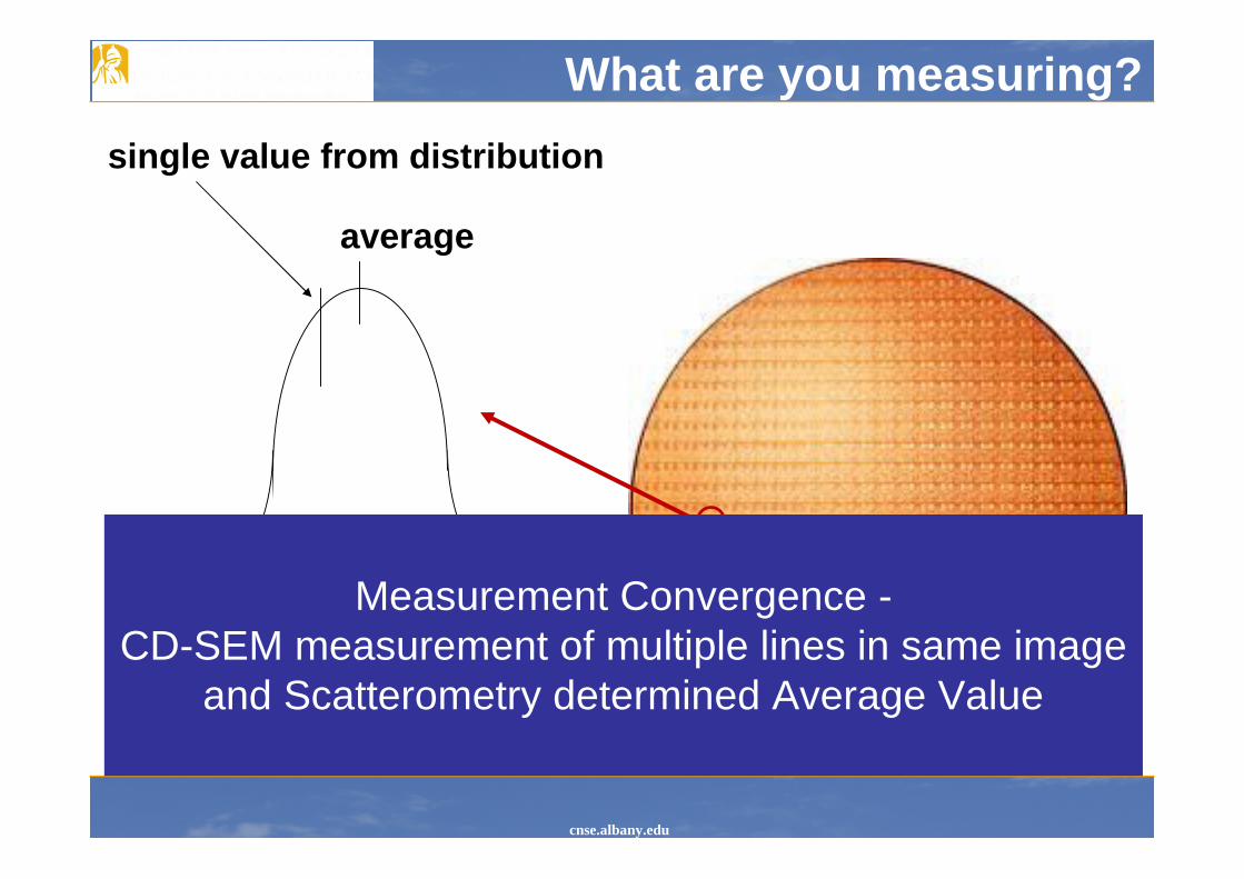
test structure inside a die
Distribution of linewidths inside test
structure
average
single value from distribution
What are you measuring?
Measurement Convergence -CD-SEM measurement of multiple lines in same image
and Scatterometry determined Average Value

cnse.albany.edu
Rotating-polarizer ellipsometry (PRSA)
D
s
p
y
Ers
Erp
RotatingPolarizer
Sample
a
RotatingAnalyzer
a’Ers
Erp
Unpolarizedincident light
Elliptically-polarized light
S
Pi
r
re =Y Dtan
Mueller Matrix
0
1
2 / 4 / 4
3
x y
x y
LCP RCP
s I I
s I IS
s I I
s I Ip p-
+é ù é ùê ú ê ú-ê ú ê ú= =ê ú ê ú-ê ú ê ú-ê ú ê úë û ë û
Stokes Vector
One example from many types of ellipsometersGreat for Isotropic Samples & No Depolarization

cnse.albany.edu
Dual Rotating Compensator Ellipsometer (RC2)
Dp
y
Ers
Erp
Rotating Compensator
Sample
a
RotatingAnalyzer
a’Ers
Erp
Unpolarizedincident light
Elliptically polarized lightRotating
Polarizer
Mueller Matrix
0
1
2 / 4 / 4
3
x y
x y
LCP RCP
s I I
s I IS
s I I
s I Ip p-
+é ù é ùê ú ê ú-ê ú ê ú= =ê ú ê ú-ê ú ê ú-ê ú ê úë û ë û
Stokes Vector
Laboratory EllipsometerGreat for All Types of Samples
Rotating Compensator

cnse.albany.edu
Optical Scatterometry Summary
• Diffraction-Based Tool - Ellipsometers / Reflectometers– Optical scatteringà average grating CD/profile – Software/model-dependent solution of CD/profile– Not imaging tool like CD-SEM, less localized info
• Pros – Fast, non-destructive, cheap CD/profile metrology– Non-vacuum à small size à standalone or integrated– High confidence measurement of average process
• Cons– Accuracy known only after verification to reference– No variation information– Grating target only, not applicable in-circuit, cannot
measure discrete features– Model solution vulnerable to shift in optical properties

cnse.albany.edu
CD-SEM Life Extension
• The useful life of CD-SEM may be extended through improved alignment and calibrations.– Drift corrected frame averaging (NIST)
– Tool matching and performance monitoring using the Contrast Transfer Function

cnse.albany.edu
Frame averaging with drift correction
Single frame
11ms frame time
70 frames
Standard frame averaging
70 frames
NIST averaging
Contour metrology can be improved through frame average if successive frames are aligned using information from interferometer based stage tracking.
Andras Vladar (NIST)
Stage position of frames

cnse.albany.edu
Contrast Transfer Function
• The Contrast Transfer Function (CTF) of a tool provides a measure of the fidelity with which sample information is transferred to the final image, as a function of spatial frequency.– Resolution limit is when the CTF falls below the noise floor.
0
20
40
60
80
100
0.0001 0.001 0.01 0.1 1
Spatial Frequency (nm-1)
% T
ran
smis
sio
n Perfect SEM
Real SEM
Noise limit
D.C. Joy, J. Michael, B. Griffin, Evaluating SEM Performance from the Contrast Transfer Function. Proc. SPIE 7638, 76383J (2010)

cnse.albany.edu
Obtaining the CTF
• The CTF can be obtained from the Fourier transformed image of a specimen with uniform power across all spatial frequencies.– Impossible to produce perfectly, but can use
• Fresnel Zone Plates
• Pseudo-random dot arrays
– Quality of transform depends on precision of specimen
• Notes:– CTF is a simplification of the Optical Transfer function appropriate for
digital images– CFT = Fourier Transform of the Point Spread Function

cnse.albany.edu
CTF Targets
CTF test structures: photoresist on silicon, prepared with e-beam written template and nano-imprint lithography with a 22 nm process.
Pseudo-random dot array Fresnel Zone Plate

cnse.albany.edu
Performance Defects
• Tool performance defects have signatures in the CTF.– Defocus– Astigmatism– Aberrations– Vibrations– Detector efficiency– External fields

cnse.albany.edu
Tracking Tool Performance
• Data corresponding to the larger feature sizes appears unchanged• Data taken in March shows a noise floor with less magnitude, which begins at smaller feature sizes
0.5
0.550.6
0.650.7
0.75
0.80.85
0.9
0.951
feature size (nm)
Optic
al T
rans
fer F
unct
ion
Jan-11
Mar-11
11001000

cnse.albany.edu
Conclusions
• Candidate solutions exist for replacing CD-SEM, but there is no clear leader.– More development is necessary
• Optical Scatterometry is currently feasible, but:– Results are strongly model & material dependent– Does not provide information on variance
• X-ray Scatterometry is not currently practical, but:– Synchrotron-based results are impressive– Significant amount of information can be extracted– Models are robust
• Fortunately, a little more life can be squeezed out of CD-SEMs