Embed Size (px)
DESCRIPTION
AIE Processor Concept. Sequential Processor Stages. Fetch. Decode. Execute. Mem. WB. Pipelining Processor Stages. Execute. Pip E line. Mem. Pip E line. WB. Fetch. Pip E line. Decode. Pip E line. Transaction Table. Five Stages Pipeline. Pipelining Design. As Queue - PowerPoint PPT Presentation
Citation preview

AIE Processor Concept
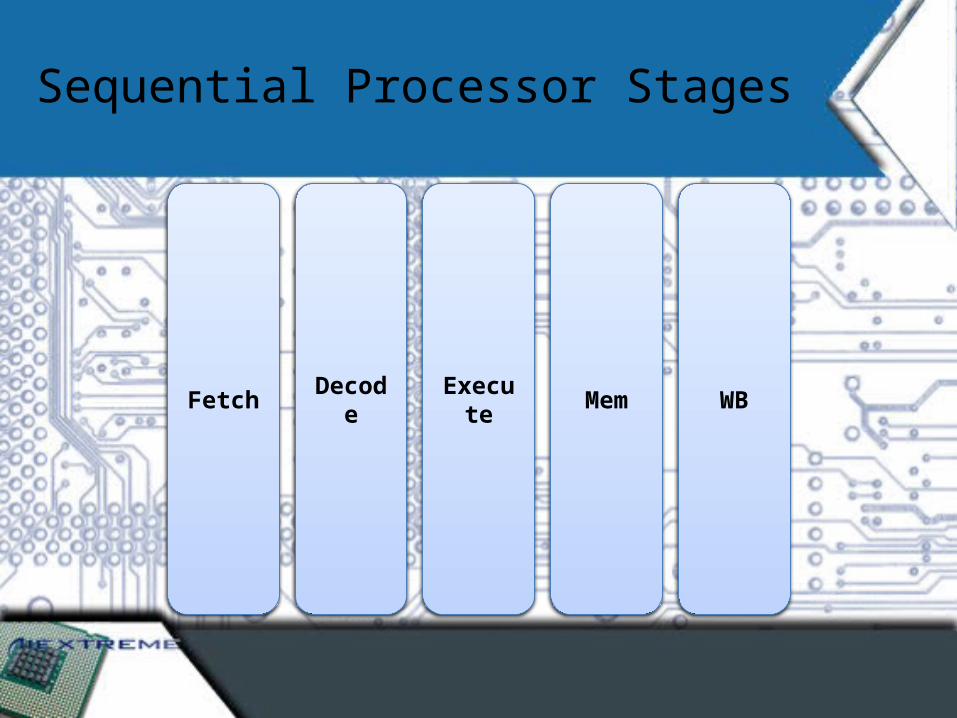
Sequential Processor Stages
DecodeFetch Execute Mem WB

Pipelining Processor Stages
DecodeFetch Execute Mem
PipEline
WB
PipEline
PipEline
PipEline
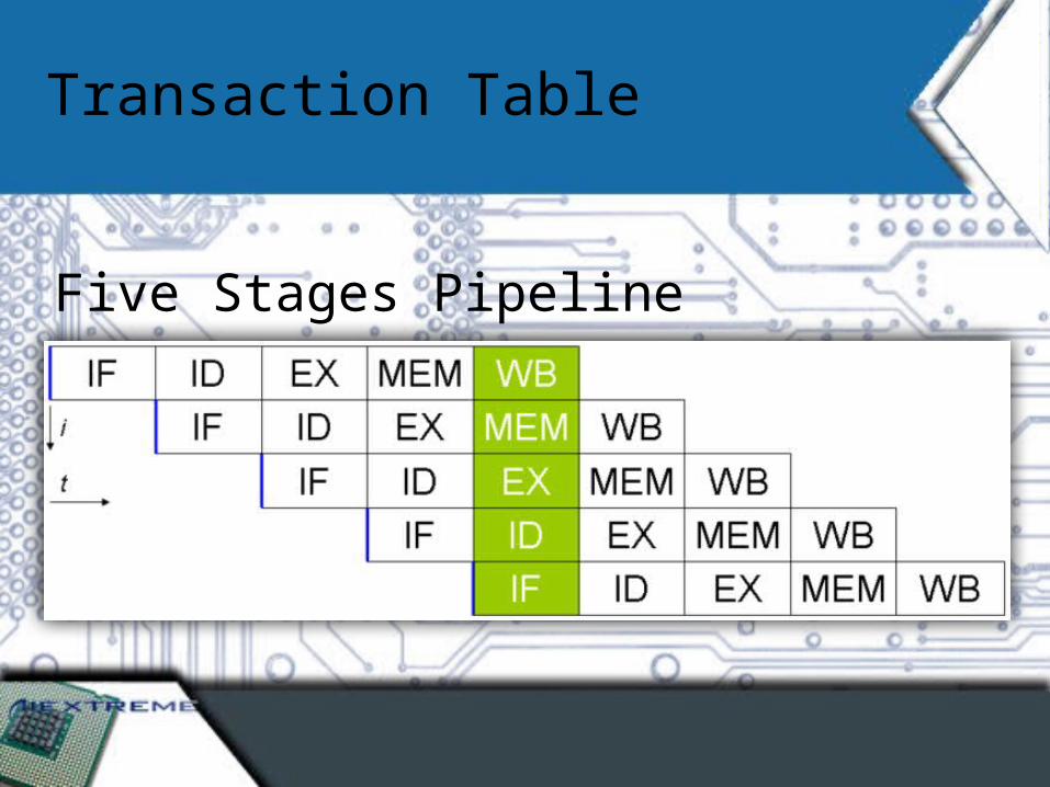
Transaction Table
Five Stages Pipeline
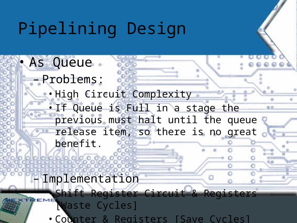
Pipelining Design
• As Queue– Problems:
• High Circuit Complexity• If Queue is Full in a stage the previous must halt until
the queue release item, so there is no great benefit.
– Implementation• Shift Register Circuit & Registers [Waste Cycles] • Counter & Registers [Save Cycles]
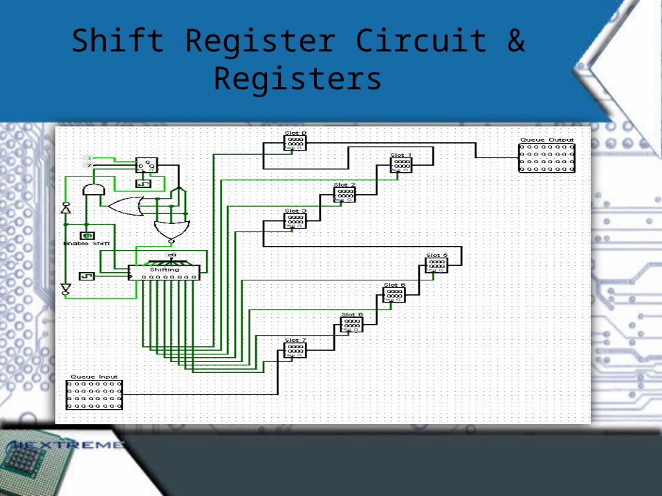
Shift Register Circuit & Registers
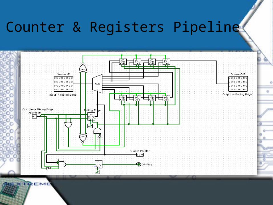
Counter & Registers Pipeline

Pipeline Optimal Designs
• Sync Pipeline– All Pipeline Modules Attached with Same Cycle
Controller– Cycle Time = Max Stage Clock– Problems
• There is Waste in Clock but not to much• Every stage not aware of the status of previous stage.
Pipeline Optimal Designs
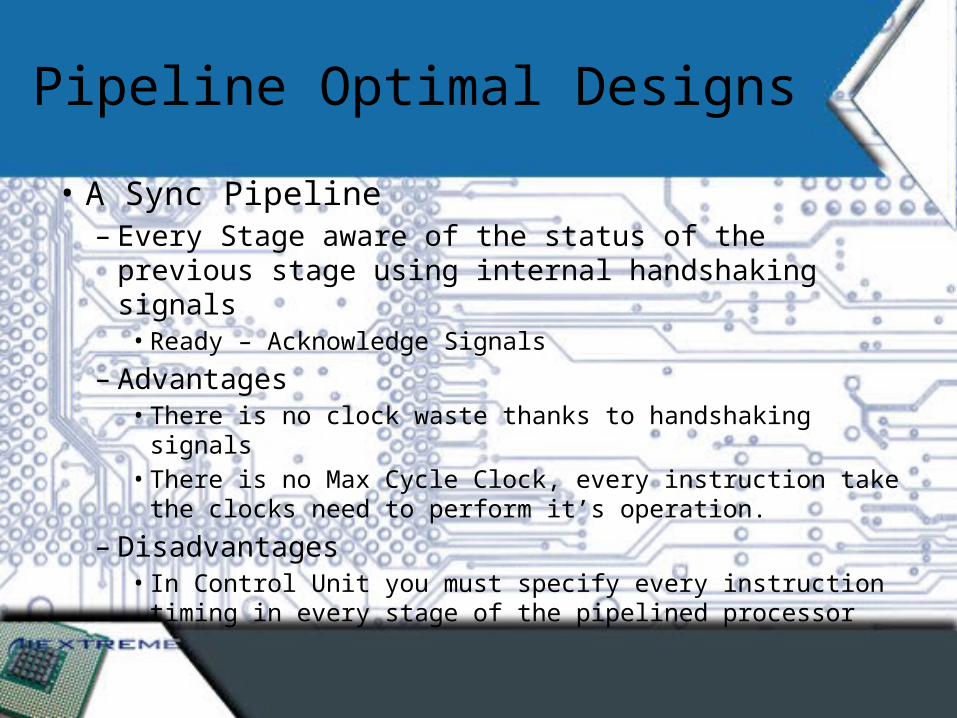
• A Sync Pipeline– Every Stage aware of the status of the previous stage
using internal handshaking signals• Ready – Acknowledge Signals
– Advantages• There is no clock waste thanks to handshaking signals• There is no Max Cycle Clock, every instruction take the
clocks need to perform it’s operation.
– Disadvantages• In Control Unit you must specify every instruction timing in
every stage of the pipelined processor
Pipeline Optimal Designs
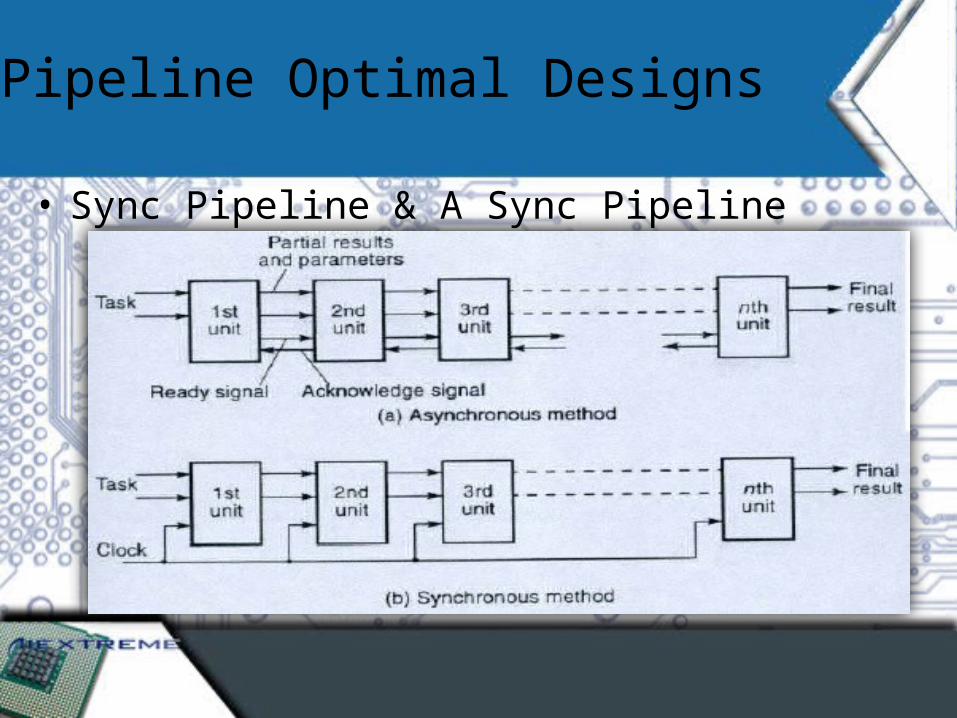
• Sync Pipeline & A Sync Pipeline

Sync Pipeline Implementation
Key Feature of AIE Processor
• 32-bit Pipelined Processor• Processor Support 48 Instruction• Processor Interface with Interleaved Memory• Interface with LCD Terminal using Instructions• Processor have it’s Assembly Interpreter

Instructions
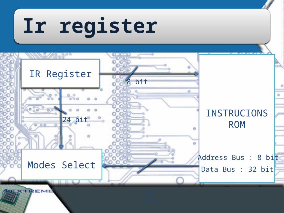
Ir register
IR Register8 bit
INSTRUCIONSROM
Address Bus : 8 bit
Data Bus : 32 bit
32 bit
Modes Select
24 bit
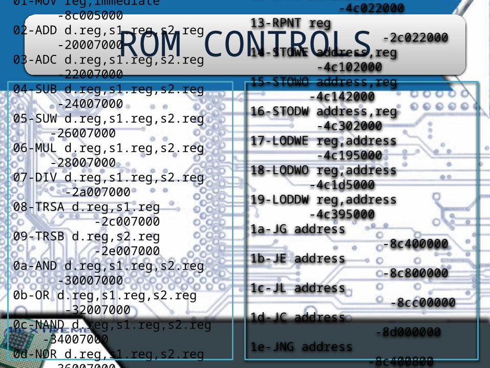
ROM CONTROLS11-CMP reg1,reg2 -3e00200012-IPNT immediate -4c02200013-RPNT reg -2c02200014-STOWE address,reg -4c10200015-STOWO address,reg -4c14200016-STODW address,reg -4c30200017-LODWE reg,address -4c19500018-LODWO reg,address -4c1d500019-LODDW reg,address -4c3950001a-JG address -8c400000 1b-JE address -8c8000001c-JL address -8cc000001d-JC address -8d0000001e-JNG address -8c400800 1f-JNE address -8c80080020-JNL address -8cc0080021-JNC address -8d00080022-JMP address -8d400000
00-NOP -0000800001-MOV reg,immediate -8c00500002-ADD d.reg,s1.reg,s2.reg -2000700003-ADC d.reg,s1.reg,s2.reg -2200700004-SUB d.reg,s1.reg,s2.reg -2400700005-SUW d.reg,s1.reg,s2.reg -2600700006-MUL d.reg,s1.reg,s2.reg -2800700007-DIV d.reg,s1.reg,s2.reg -2a00700008-TRSA d.reg,s1.reg -2c00700009-TRSB d.reg,s2.reg -2e0070000a-AND d.reg,s1.reg,s2.reg -300070000b-OR d.reg,s1.reg,s2.reg -320070000c-NAND d.reg,s1.reg,s2.reg -340070000d-NOR d.reg,s1.reg,s2.reg -360070000e-XOR d.reg,s1.reg,s2.reg -380070000f-XNOR d.reg,s1.reg,s2.reg -3a00700010-NOT d.reg,s1.reg -3c007000
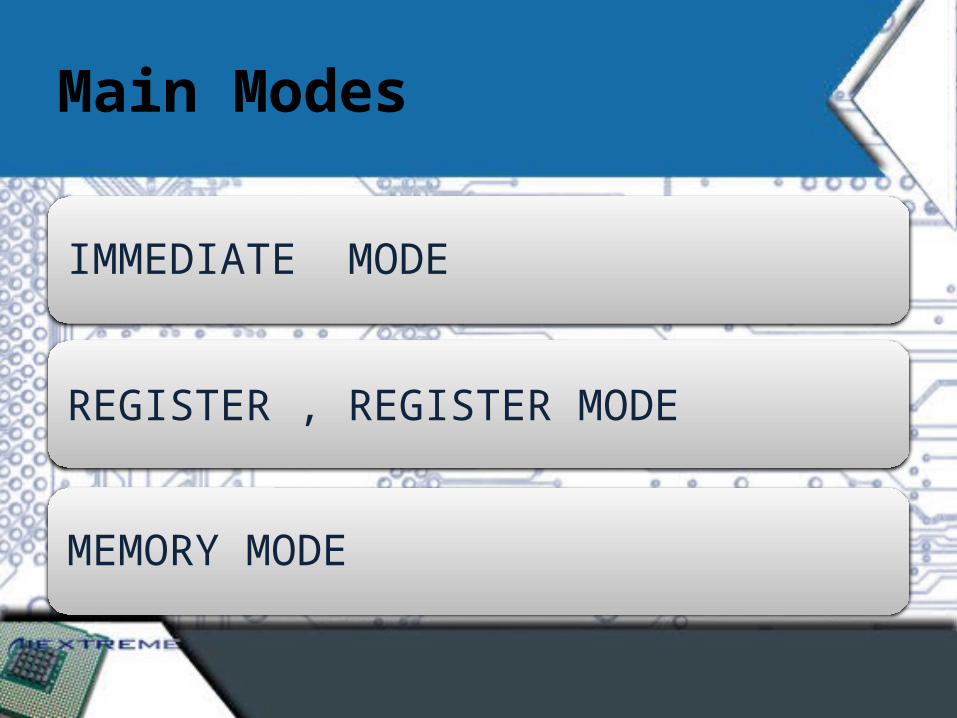
Main Modes
IMMEDIATE MODE
REGISTER , REGISTER MODE
MEMORY MODE
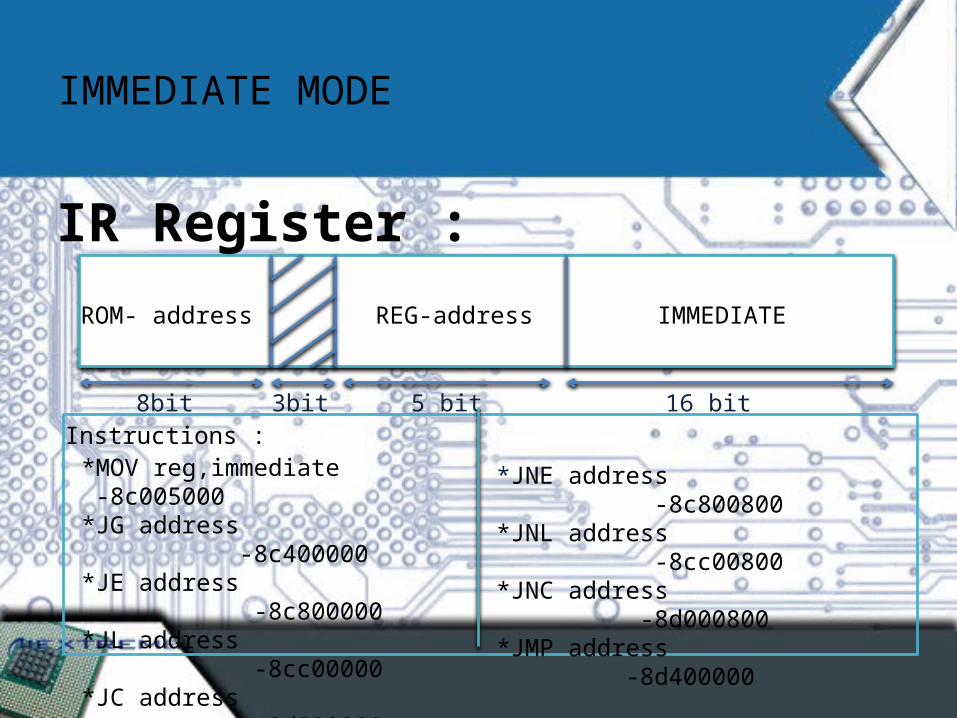
IMMEDIATE MODE
ROM- address
8bit
REG-address
5 bit3bit
IMMEDIATE
16 bit
IR Register :
Instructions :*MOV reg,immediate -8c005000*JG address -8c400000 *JE address -8c800000*JL address -8cc00000*JC address -8d000000*JNG address -8c400800
*JNE address -8c800800*JNL address -8cc00800*JNC address -8d000800*JMP address -8d400000
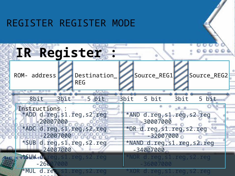
REGISTER REGISTER MODE
IR Register :
ROM- address
8bit
Source_REG2
5 bit3bit
Source_REG1
5 bit3bit
Destination_REG
5 bit3bit
Instructions :*ADD d.reg,s1.reg,s2.reg -20007000*ADC d.reg,s1.reg,s2.reg -22007000*SUB d.reg,s1.reg,s2.reg -24007000*SUW d.reg,s1.reg,s2.reg -26007000*MUL d.reg,s1.reg,s2.reg -28007000*DIV d.reg,s1.reg,s2.reg -2a007000*TRSA d.reg,s1.reg -2c007000*TRSB d.reg,s2.reg -2e007000
*AND d.reg,s1.reg,s2.reg -30007000*OR d.reg,s1.reg,s2.reg -32007000*NAND d.reg,s1.reg,s2.reg -34007000*NOR d.reg,s1.reg,s2.reg -36007000*XOR d.reg,s1.reg,s2.reg -38007000*XNOR d.reg,s1.reg,s2.reg -3a007000*NOT d.reg,s1.reg -3c007000*CMP reg1,reg2 -3e002000
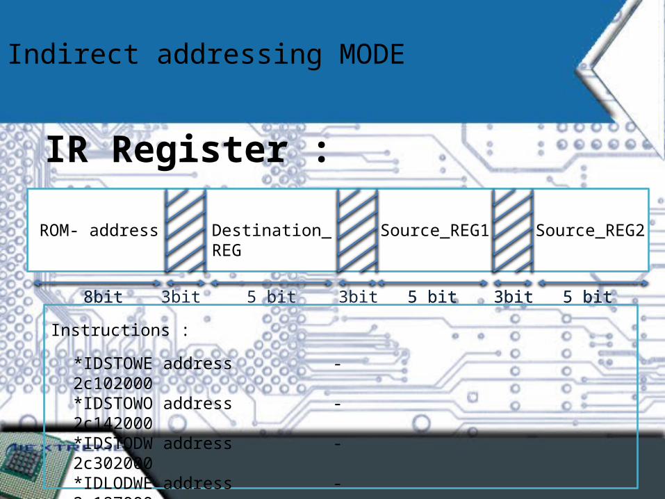
Indirect addressing MODE
IR Register :
8bit 5 bit3bit5 bit
Instructions :
*IDSTOWE address - 2c102000*IDSTOWO address - 2c142000*IDSTODW address - 2c302000*IDLODWE address - 2c187000*IDLODWO address - 2c1c7000*IDLODDW address - 2c387000
ROM- address
8bit
Source_REG2
5 bit3bit
Source_REG1
5 bit3bit
Destination_REG
5 bit3bit

MEMORY MODE
IR Register :
ROM- address
8bit
IMMEDIATE
16 bit
REG-address
3bit 5 bit
Instructions :*STOWE address,reg -4c102000*STOWO address,reg -4c142000*STODW address,reg -4c302000*LODWE reg,address -4c195000*LODWO reg,address -4c1d5000*INC reg,immediate - 40007000*DEC reg,immediate -44007000
*LODDW reg,address -4c395000*IPNT immediate -4c022000*PUSHWE reg -4c102400*PUSHWO reg -4c142400*PUSHDW reg -4c302400*POPWE reg -4c195600*POPWO reg -4c1d5600*POPDW reg -4c395600
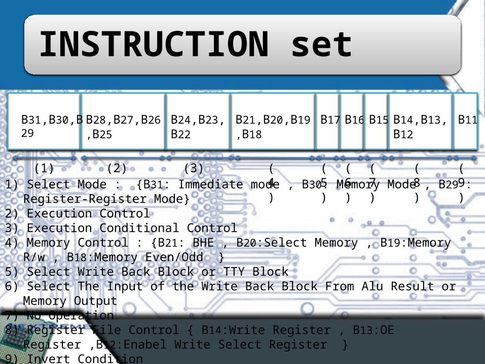
INSTRUCTION set
B31,B30,B29
(1)
B28,B27,B26,B25
(2)
B24,B23,B22
(3)
B21,B20,B19,B18
(4)
B17 B16 B15 B14,B13,B12 B11
(5) (6) (7) (8) (9)1) Select Mode : {B31: Immediate mode , B30: Memory Mode , B29 : Register-Register Mode}2) Execution Control3) Execution Conditional Control4) Memory Control : {B21: BHE , B20:Select Memory , B19:Memory R/w , B18:Memory Even/Odd }5) Select Write Back Block or TTY Block6) Select The Input of the Write Back Block From Alu Result or Memory Output7) No Operation8) Register File Control { B14:Write Register , B13:OE Register ,B12:Enabel Write Select Register }9) Invert Condition

Tracing Some Instructions
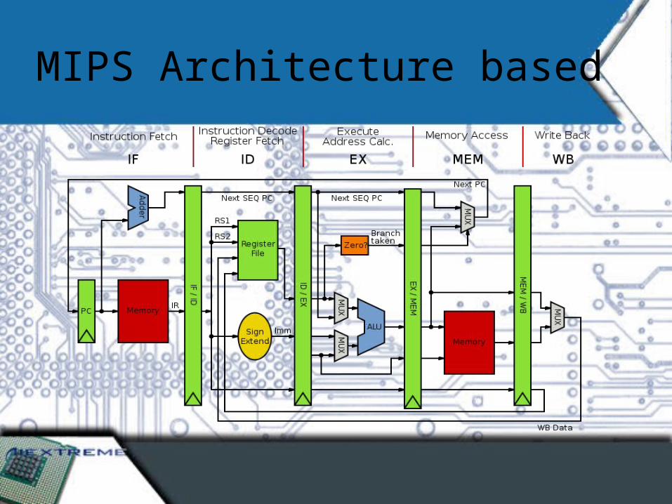
MIPS Architecture based
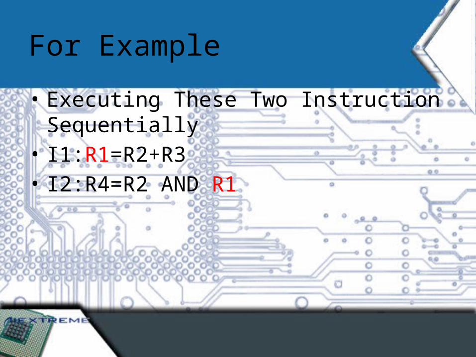
For Example
• Executing These Two Instruction Sequentially • I1:R1=R2+R3• I2:R4=R2 AND R1
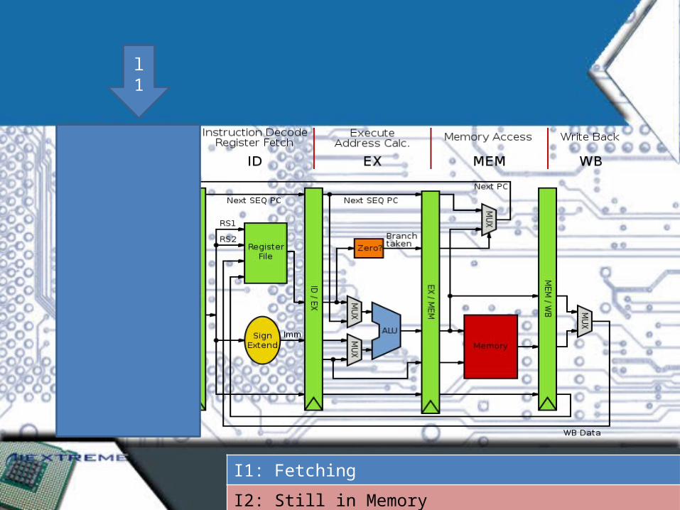
I1: Fetching
I2: Still in Memory
l1
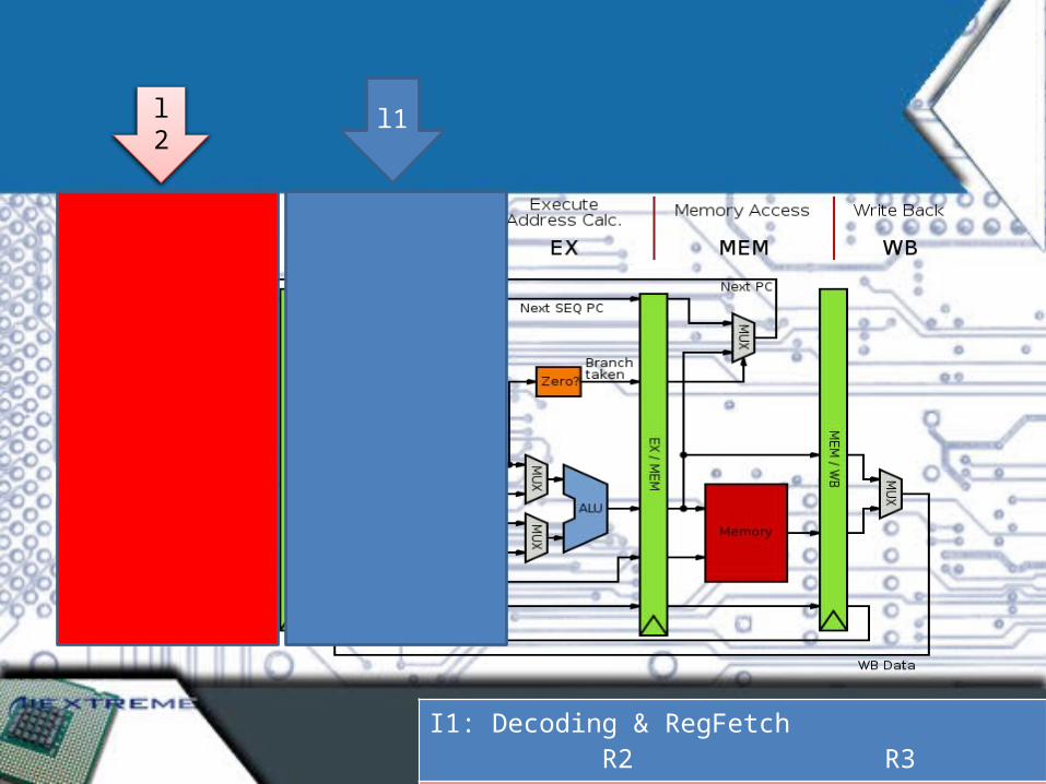
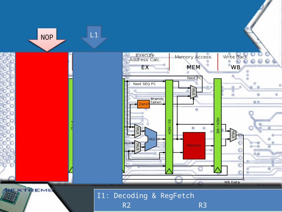
I1: Decoding & RegFetch R2 R3
I2: Fetching
l2 l1

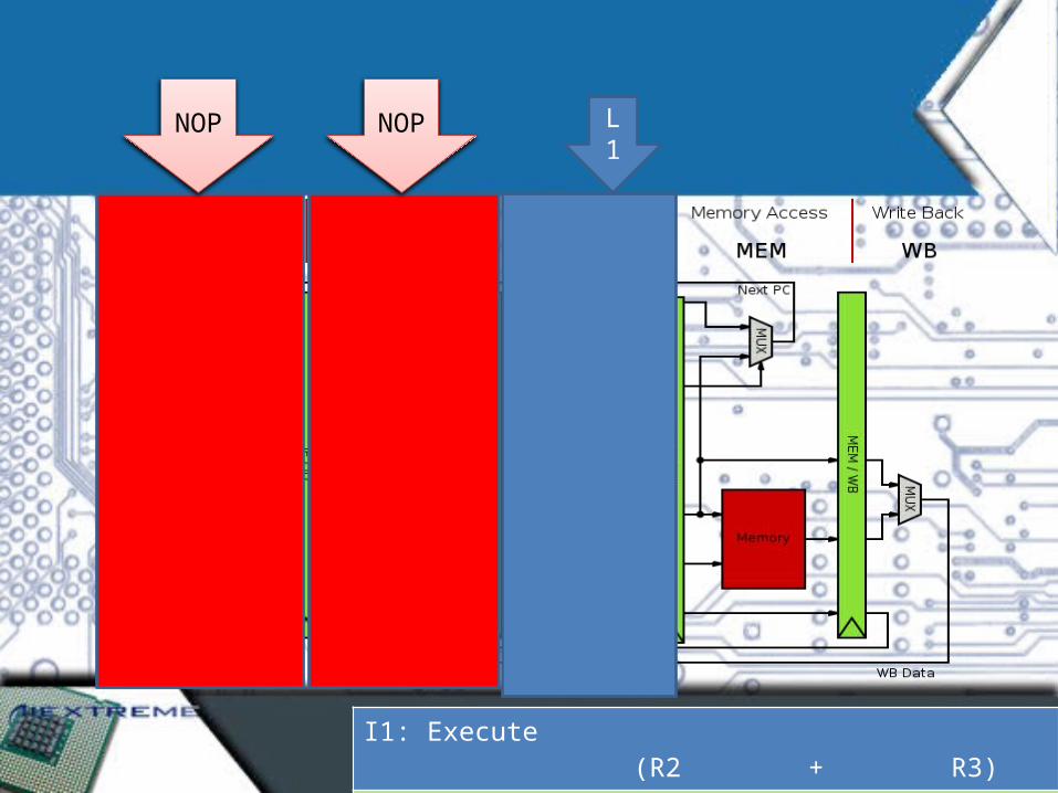
I1: Execute (R2 + R3)
I2: Decoding & RegFetch R2 R1
l2 l1

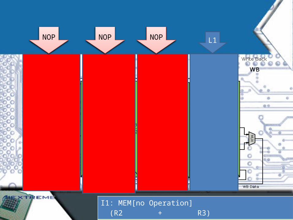
I1: MEM[no Operation] (R2 + R3)
I2: Execute (R2 AND R1)
l2 l1

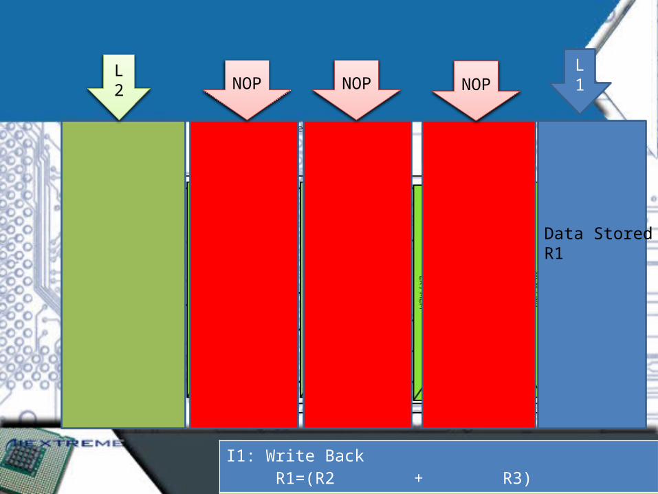
I1: Write Back R1=(R2 + R3)
I2: MEM[no Operation] (R2 AND R1)
Data Stored In R1
l2 l1
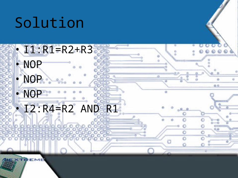
Solution
• I1:R1=R2+R3• NOP• NOP• NOP• I2:R4=R2 AND R1

I1: Fetching
I2: Still in Memory
l1
I1: Decoding & RegFetch R2 R3
I2: Still in Memory
L1NOP
I1: Execute (R2 + R3)
I2: Still in Memory
NOP L1NOP
I1: MEM[no Operation] (R2 + R3)
I2: Still in Memory
NOP L1NOPNOP
I1: Write Back R1=(R2 + R3)
I2: Fetching
Data Stored In R1
L1NOPNOP NOPL2
I1: Terminated
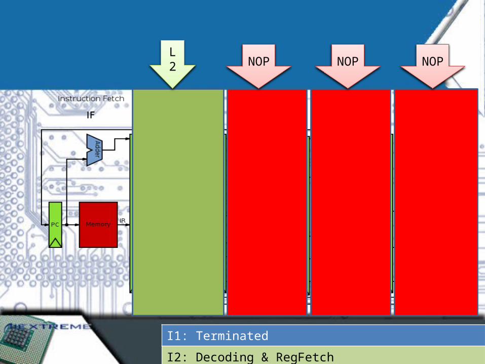
I2: Decoding & RegFetch R2 R1
L2 NOP NOP NOP
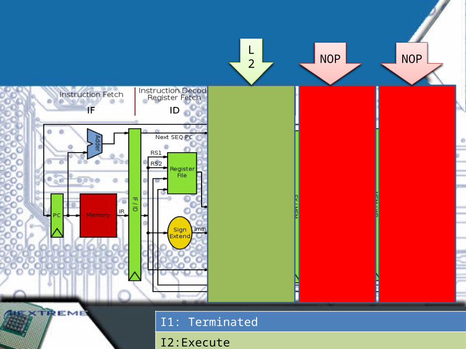
I1: Terminated
I2:Execute (R2 AND R1)
L2 NOP NOP
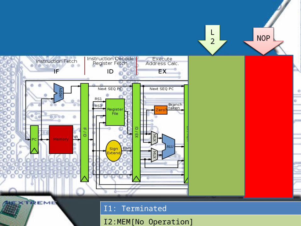
I1: Terminated
I2:MEM[No Operation] (R2 AND R1)
L2 NOP
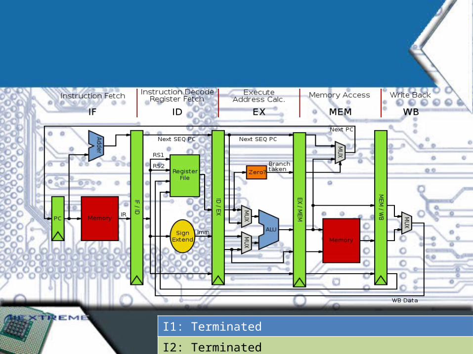
I1: Terminated
I2: Terminated

Statistics & Comparisons

Cisc Vs RiscCisc:
-Richer instruction set but very complex circuit.-Instructions generally take more than 1 clock to execute.-Instructions of a variable size.Risc:-Instructions execute in one clock cycle.-Uniformed length instructions and fixed instruction format.-Simple instructions and circuit.
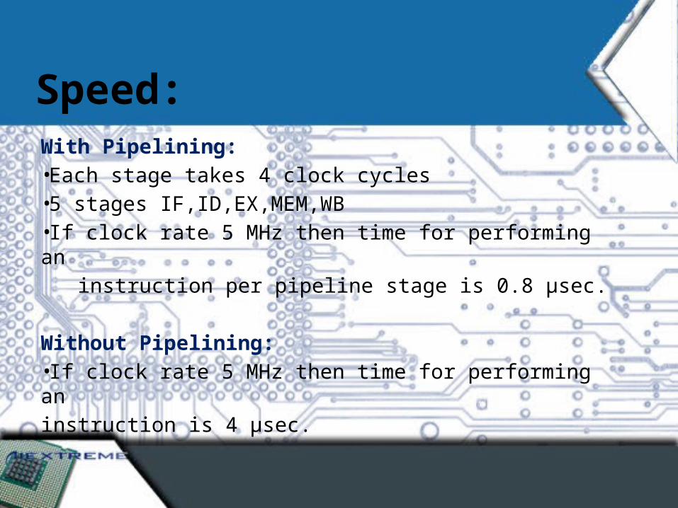
Speed:With Pipelining:•Each stage takes 4 clock cycles•5 stages IF,ID,EX,MEM,WB•If clock rate 5 MHz then time for performing an
instruction per pipeline stage is 0.8 µsec.
Without Pipelining:•If clock rate 5 MHz then time for performing an
instruction is 4 µsec.
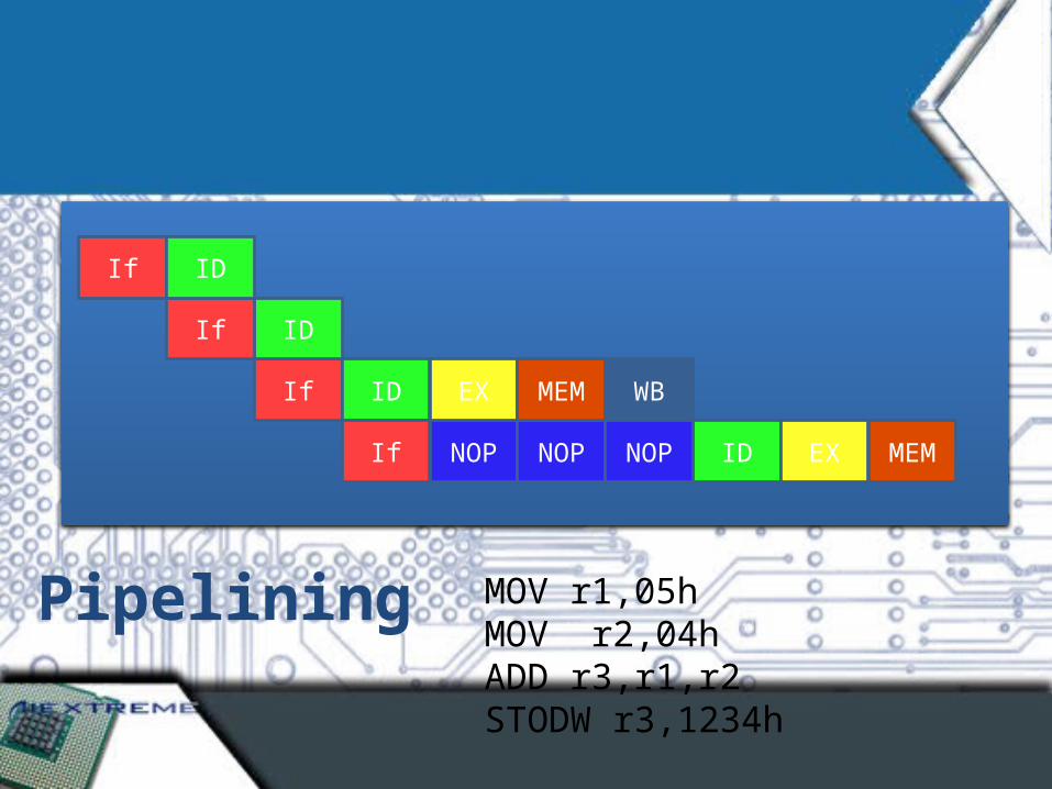
MOV r1,05hMOV r2,04hADD r3,r1,r2STODW r3,1234h
Pipelining
If
ID
NOP NOP
If
If ID
ID EX MEM
If ID EX MEM
WB
NOP
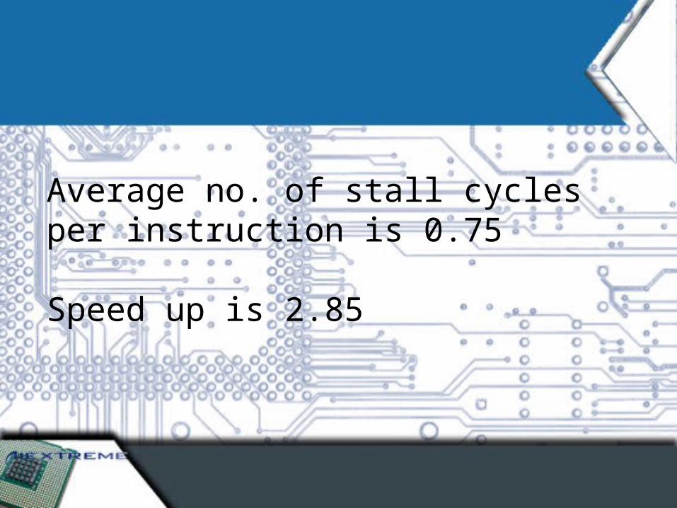
Average no. of stall cycles per instruction is 0.75
Speed up is 2.85

Thank you