Embed Size (px)
Citation preview

Lithography Challenges
Andrzej J. Strojwas
Carnegie Mellon UniversityCenter for Silicon System Implementation
&PDF Solutions, Inc.
Designing Robust Digital Circuits,C2S2 Workshop, UCB, July 27, 2006

2
A. J. Strojwas, C2S2 Workshop, UCB, July 27, 2006
Projection of MOSFET scaling
Source: Intel

3
A. J. Strojwas, C2S2 Workshop, UCB, July 27, 2006
Transistor Ioff Leakage Challenge
Source: Intel

4
A. J. Strojwas, C2S2 Workshop, UCB, July 27, 2006
Optical Lithography Evolution
i193 (immer.)λ=193nm
5
A. J. Strojwas, C2S2 Workshop, UCB, July 27, 2006
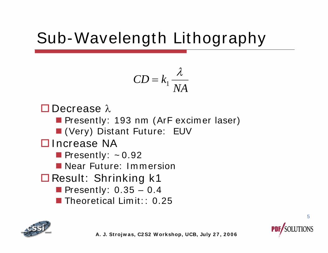
Sub-Wavelength Lithography
Decrease λPresently: 193 nm (ArF excimer laser)(Very) Distant Future: EUV
Increase NAPresently: ~0.92Near Future: Immersion
Result: Shrinking k1Presently: 0.35 – 0.4Theoretical Limit:: 0.25
NAkCD λ
1=

6
A. J. Strojwas, C2S2 Workshop, UCB, July 27, 2006
Printability Issues
Sensitive to exposure and defocusHighly neighborhood dependentStrong RETs are necessary @ k1 << 0.5
Source: Liebmann, IBM, ISPD-2003

7
A. J. Strojwas, C2S2 Workshop, UCB, July 27, 2006
Sub-Wavelength Lithography
Depth Of Focus (DOF)The amount by which the distance between lens and wafer can be varied without adversely affecting image quality
Larger DOF desiredImprovements in resolution decrease DOFStringent requirement on wafer planarity
( )22 NAkDOF λ
=

8
A. J. Strojwas, C2S2 Workshop, UCB, July 27, 2006
Integration and Litho Breakthroughs
DUV ScannerChemically Amplified ResistDie by Die Leveling
Hi NA DUVPartial Coherence / NAGC Rule base OPC
193 nmAtt Phase shift maskRule Base OPC
Model based OPCAssist FeaturesHi NA 193nm
Few new RET techniquesPervasive Assist+MBOPC
Immersion Litho
1994 1996 1999 2002 2005
Dose Lat 4-5%Focus 0.25 um
Dose Lat 5%Focus 0.35 um
DO
F 1
..0um
DoseLat 15%
Dose Lat 7.5%Focus 0.5 um
DO
F 0
.75m
DoseLat 10%
2008
Key Litho Breakthrough
SOI FEOL RX IsolationAl / Oxide multi-layersChem Mech Polish (oxide)
Halo engineeringCu / oxide Damascene BEOLCu ElectroplateCu Polish
Cu / Low K (FSG) BEOLTriple Gate oxideeDRAM / SOCCu / Low K (SiCOH) BEOLMulti-Vt Device offeringSome Strain Eng.
FEOL:Strained SiliconFEOL: NiSiRaised Source/Drain?Lower K BEOL ?New device structures
Key Integration Changes

9
A. J. Strojwas, C2S2 Workshop, UCB, July 27, 2006
65 nm: No Major Litho Breakthrough
Dose Lat 4-5%Focus 0.25 um
Dose Lat 5%Focus 0.35 um
Tech
nolo
gy N
ode
(nm
)
80
240
120
160
200
40
1994 1996 1999 2002 2005 2008
DUV ScannerChemically Amplified ResistDie by Die Leveling
Hi NA DUVPartial Coherence / NAGC Rule base OPC
193 nmAtt Phase shift maskRule Base OPC
Model based OPCAssist FeaturesHi NA 193nm
Few new Enhancement techniquesPervasive Assist+MBOPC
Immersion Litho
Key Litho Breakthrough
Gate – Alt. PSM 2 exposures
M1 - Not New
Shrinking Process Window
DO
F 1
..0um
DoseLat 15%
DO
F 0
.75m
DoseLat 10%
Dose Lat 7.5%Focus 0.5 um

10
A. J. Strojwas, C2S2 Workshop, UCB, July 27, 2006
Sources of Poly CD VariationsNPoly: Variance Components
0.00
50.00
100.00
150.00
200.00
0.09 0.10 0.11 0.12 0.14 0.30
Ldrawn (um)
Varia
nce/
Varia
nce@
100n
m(%
)
L2LW2WD2DWithin-Field
Nor
mal
ized
Var
ianc
e
N+ poly ACV Decomposition
0%
20%
40%
60%
80%
100%
0.09 0.1 0.11 0.12 0.14 0.3
Lpoly
% W
ID Random ACVSytematic ACV
Within Field variations dominate
Systematic variation contribution increases with scaling

11
A. J. Strojwas, C2S2 Workshop, UCB, July 27, 2006
Line Edge Roughness
3σ=18.9%
-20 -10 0 10 200
24
68
10Er
Count
Random variations mostly due to resist effects
LER(i) = Lg(i)-Lg_ave

12
A. J. Strojwas, C2S2 Workshop, UCB, July 27, 2006
Layout-Dependent Variations
Significant increase in variation magnitudes and pattern dependency with decreasing feature sizes
Identical min size transistors measured for three different physical environments on the same 65nm IC
Much of this problem is attributable to the use of sub-wavelength lithography to print critical dimensions
Source: PDF Solutions
-10.50-10.00-9.50-9.00-8.50-8.00
-7.00
-6.00
300.00 400.00 500.00 600.00 700.00 800.00IdriveIo
ff(lo
g)Env I Env II Env III

13
A. J. Strojwas, C2S2 Workshop, UCB, July 27, 2006
RETs
Optical Proximity Correction (OPC)Model based is computationally intensiveRule based is inaccurate
Sub Resolution Assist FeaturesForbidden pitches must be avoided
alternating Phase Shift MaskPhase conflicts need to be resolved

14
A. J. Strojwas, C2S2 Workshop, UCB, July 27, 2006
RET Application ChallengesRETs developed for nominal litho conditions butNot robust across process windows
Defocus, Exposure dose, misalignment, lens aberrations, mask error enhancement factor, resist and etch processing
Number of layout patterns within interaction radius grows rapidly with feature scaling
CD SEM Data Across focus

15
A. J. Strojwas, C2S2 Workshop, UCB, July 27, 2006
Product Hot Spot: Poly LayerSimulation Observations:
Line shrink due to process variationsOPC tries to correct corner rounding in nominal litho conditions.Very High focus sensitivityCan only be improved by DFM
focusNominal
CDSEM Data -Across focus

16
A. J. Strojwas, C2S2 Workshop, UCB, July 27, 2006
M1 Line End Pull Back with OPC Issues
Multi-layer analysis shows significant line end pull back and sensitivity to exposure condition and mask enhancement error factor (MEEF)
missing OPC good OPC Insufficient OPC: 3-sided minimumspace restrictions,lower misalignmentmargin.
OPC optimization issue: neighbors ok butinsufficient OPC in the middle
Missing OPC correction:interaction design style
and OPC

17
A. J. Strojwas, C2S2 Workshop, UCB, July 27, 2006
Restrictive Design Rules for Logic?
IBM 65nm Restrictive Design Rules (RDR) , Liebmann, Lavin, et al.
Grid/glyph based diagram followed by layout elaboration (generation)Easy to migrate the existing design into different RDR Less litho variation
Elaboration Step
M Lavin et al, ICCAD - 2004

18
A. J. Strojwas, C2S2 Workshop, UCB, July 27, 2006
Litho-Friendly DFM SRAM Designs
Intel’s 65nm SRAM (k1=.45)
Double exposure solution for 45nm gives k1=.38Source: Y. Borodovsky, Intel, SPIE-2006

19
A. J. Strojwas, C2S2 Workshop, UCB, July 27, 2006
Immersion Litho to the Rescue
Process Window for Dry LithoSource: B. Lin, TSMC, IEDM-2005

20
A. J. Strojwas, C2S2 Workshop, UCB, July 27, 2006
Immersion Litho to the Rescue
Process Window for Immersion LithoSource: B. Lin, TSMC, IEDM-2005

21
A. J. Strojwas, C2S2 Workshop, UCB, July 27, 2006
45nm Immersion Litho (193i)
45nm MP/32nm
TD2007TWINSCAN
XT:1900i1.35ASML
45nm MP
45nm MP and 32nm
TD
55nm MP and 45nm
TD
45nm MP
Node
Q1/2007
2H/2006
Q4/2005
Q1/2006
Year
NSR-S609B1.07Nikon
NSR-S610C1.3Nikon
SPIE 2006SEMICON West 2006
TWINSCAN XT:1700i1.2ASML
FPA70001.3Canon
SourcesmodelHyper NAVendor
22
A. J. Strojwas, C2S2 Workshop, UCB, July 27, 2006
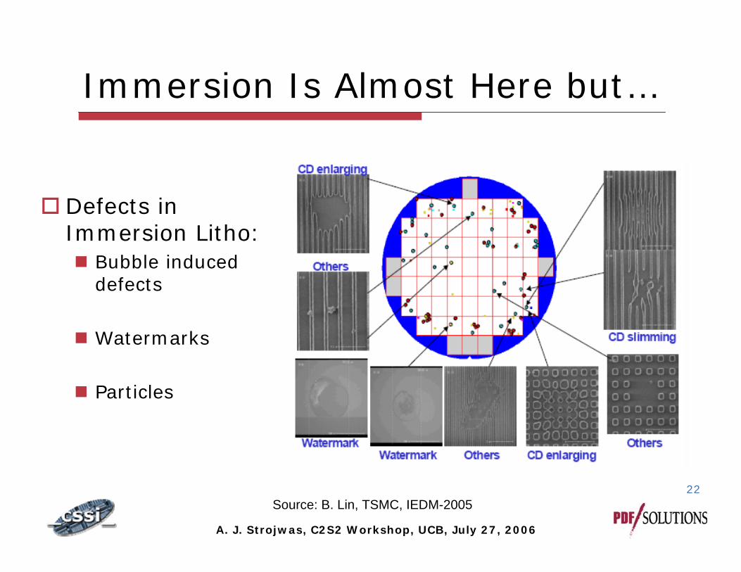
Immersion Is Almost Here but…
Defects in Immersion Litho:
Bubble induced defects
Watermarks
Particles
Source: B. Lin, TSMC, IEDM-2005

23
A. J. Strojwas, C2S2 Workshop, UCB, July 27, 2006
Going Below 45nm
Irregular contact hole printing is first casualty
Insufficient DOF
Expensive double-exposure solutions:Pack-and-cover techniquePitch splitting technique

24
A. J. Strojwas, C2S2 Workshop, UCB, July 27, 2006
Pack-and-Cover Technique
Source: B. Lin, TSMC, IEDM-2005

25
A. J. Strojwas, C2S2 Workshop, UCB, July 27, 2006
Pitch Splitting Technique
Source: B. Lin, TSMC, IEDM-2005

26
A. J. Strojwas, C2S2 Workshop, UCB, July 27, 2006
Summary of Solutions
RDR’s for Logic:Mostly for PolySignificant area penalty (up to 30%)
SRAM’s:altPSM and separate patterning for array and periphery
Expensive manufacturing solutions for random logic layout:
Immersion lithoDouble exposure techniquesPolarized illumination

27
A. J. Strojwas, C2S2 Workshop, UCB, July 27, 2006
Extremely Regular Layout
Extremely Regular Layout Gratings with very few pitches on Poly, M1 & M2Contacts on the gridAllows for sub-design (push) rules
No area or performance penaltySimple Rule-Based OPC
Demonstrated in NECEL’s 55nm technologyAllows for illumination optimization (transparency in attenuated PSM, light source)
28
A. J. Strojwas, C2S2 Workshop, UCB, July 27, 2006
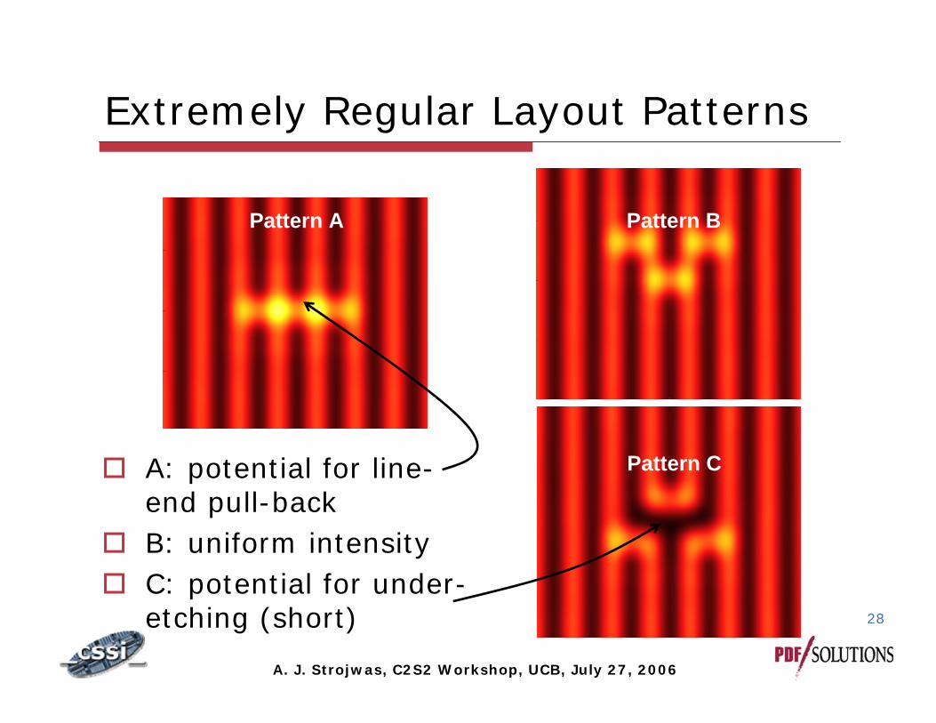
Extremely Regular Layout Patterns
A: potential for line-end pull-backB: uniform intensityC: potential for under-etching (short)
Pattern A Pattern B
Pattern C

29
A. J. Strojwas, C2S2 Workshop, UCB, July 27, 2006
Process Window OptimizationPattern B accommodates greater illumination threshold variance and depth of focus
Pattern C
Pattern A
Pattern B
Required Process Window

30
A. J. Strojwas, C2S2 Workshop, UCB, July 27, 2006
Regularity Enables Push-RulesDesign Rules are created for worst caseCan push the rules for lithography friendly patterns
Design rules are derived to work for worst case layout patterns

31
A. J. Strojwas, C2S2 Workshop, UCB, July 27, 2006
Push-Rules: Area vs. Manufacturability
Pattern B
Example: can push distance between metal line-ends down for lithography-friendly pattern B
Required Process Window

32
A. J. Strojwas, C2S2 Workshop, UCB, July 27, 2006
32nm and Below Litho Alternatives
Hyper-NA Immersion Lithohigh index fluid (>1.6)pitch-splitting masks
Interference Lithographye.g., Composite Optical Lithography (COOL)
High-voltage and low voltage multi-Ebeam direct write systems
Larger DOF but smaller throughput
Extreme UV (EUV) lithography

33
A. J. Strojwas, C2S2 Workshop, UCB, July 27, 2006
EUV
Lithographer’s life is good again λ=13.4nm so NA can be reduced to .25k1= .6Better DOF
BUT…No transparent materials yet for lens, mask or pellicleExtremely complex multi-layer masks (reflection based technique) requiring super accuracy and defectivity controlSources with adequate power not available

34
A. J. Strojwas, C2S2 Workshop, UCB, July 27, 2006
Litho Alternatives for 32 nm and Below
Source: B. Lin, TSMC, IEDM-2005

35
A. J. Strojwas, C2S2 Workshop, UCB, July 27, 2006
Conclusions
Despite soaring equipment and mask costs, optical litho will remain the key driver for the next 3 technology generations
Product volume decides if we can afford full mask setIn the foreseeable future it will contribute significantly to performance and yield variabilityMost IDM’s started and will continue on the path of RDR’s
but area penalty is troublesome (negates the move to the next technology node)
Extremely regular layout techniques look promisingbut must deal with a huge legacy of current design methodologies
EUV will help when/if it happens but we better get ready for the next 5—10 years of design challenges