Embed Size (px)
Citation preview
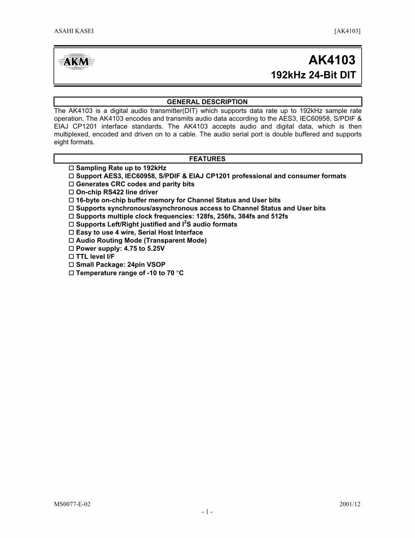
ASAHI KASEI [AK4103]
MS0077-E-02 2001/12
- 1 -
GENERAL DESCRIPTION The AK4103 is a digital audio transmitter(DIT) which supports data rate up to 192kHz sample rate operation. The AK4103 encodes and transmits audio data according to the AES3, IEC60958, S/PDIF & EIAJ CP1201 interface standards. The AK4103 accepts audio and digital data, which is then multiplexed, encoded and driven on to a cable. The audio serial port is double buffered and supports eight formats.
FEATURES Sampling Rate up to 192kHz Support AES3, IEC60958, S/PDIF & EIAJ CP1201 professional and consumer formats Generates CRC codes and parity bits On-chip RS422 line driver 16-byte on-chip buffer memory for Channel Status and User bits Supports synchronous/asynchronous access to Channel Status and User bits Supports multiple clock frequencies: 128fs, 256fs, 384fs and 512fs Supports Left/Right justified and I2S audio formats Easy to use 4 wire, Serial Host Interface Audio Routing Mode (Transparent Mode) Power supply: 4.75 to 5.25V TTL level I/F
Small Package: 24pin VSOP
Temperature range of -10 to 70 °C
192kHz 24-Bit DITAK4103
ASAHI KASEI [AK4103]
MS0077-E-02 2001/12
- 2 -
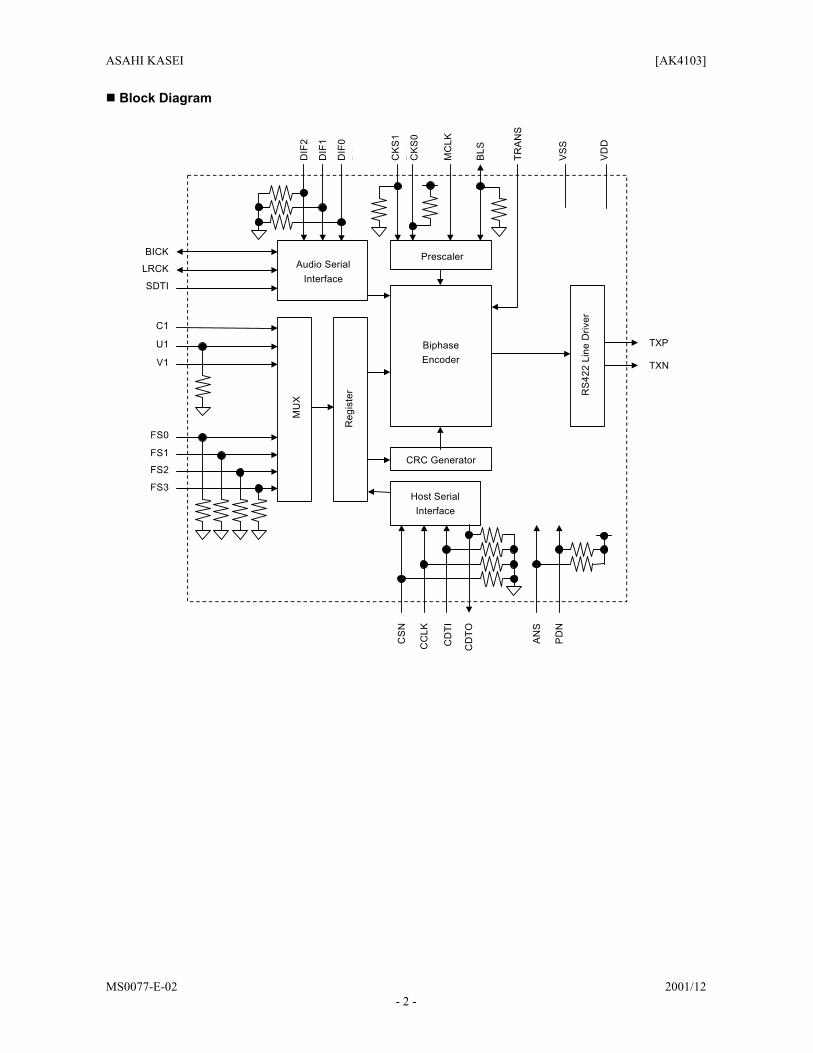
Block Diagram
Host Serial
Interface
Audio Serial
Interface
BICK
LRCK
SDTI
TXP
MU
X
CRC Generator
Prescaler
RS
422
Line
Driv
er
Biphase
Encoder
DIF
2
Di
DIF
1
Di
DIF
0
Di
CK
S1
Di
CK
S0
MC
LK
BLS
TR
AN
S
VS
S
Di
VD
D
Di
TXN
C1
U1
V1
FS0
FS1
FS2
FS3
Reg
iste
r
CS
N
CC
LK
CD
TI
CD
TO
AN
S
PD
N
ASAHI KASEI [AK4103]
MS0077-E-02 2001/12
- 3 -
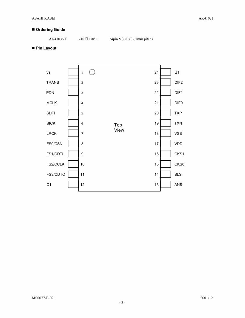
Ordering Guide
AK4103VF -10 ∼ +70°C 24pin VSOP (0.65mm pitch)
Pin Layout
6
5
4
3
2
1V1
TRANS
MCLK
PDN
SDTI
BICK
LRCK 7
FS0/CSN 8
U1
DIF2
DIF1
DIF0
TXP
TXN
VSS
VDD
TopView
10
9FS1/CDTI
FS2/CCLK
FS3/CDTO 11
C1 12
CKS1
CKS0
BLS
ANS
19
20
21
22
23
24
18
17
15
16
14
13
ASAHI KASEI [AK4103]
MS0077-E-02 2001/12
- 4 -
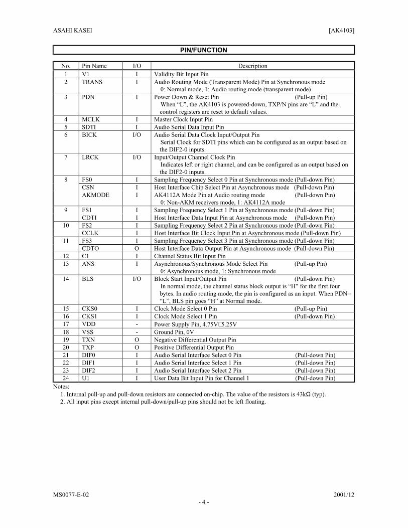
PIN/FUNCTION
No. Pin Name I/O Description
1 V1 I Validity Bit Input Pin
2 TRANS I Audio Routing Mode (Transparent Mode) Pin at Synchronous mode
0: Normal mode, 1: Audio routing mode (transparent mode)
3 PDN I Power Down & Reset Pin (Pull-up Pin)
When “L”, the AK4103 is powered-down, TXP/N pins are “L” and the
control registers are reset to default values.
4 MCLK I Master Clock Input Pin
5 SDTI I Audio Serial Data Input Pin
6 BICK I/O Audio Serial Data Clock Input/Output Pin
Serial Clock for SDTI pins which can be configured as an output based on
the DIF2-0 inputs.
7 LRCK I/O Input/Output Channel Clock Pin
Indicates left or right channel, and can be configured as an output based on
the DIF2-0 inputs.
FS0 I Sampling Frequency Select 0 Pin at Synchronous mode (Pull-down Pin)
CSN I Host Interface Chip Select Pin at Asynchronous mode (Pull-down Pin)
8
AKMODE I AK4112A Mode Pin at Audio routing mode (Pull-down Pin)
0: Non-AKM receivers mode, 1: AK4112A mode
FS1 I Sampling Frequency Select 1 Pin at Synchronous mode (Pull-down Pin) 9
CDTI I Host Interface Data Input Pin at Asynchronous mode (Pull-down Pin)
FS2 I Sampling Frequency Select 2 Pin at Synchronous mode (Pull-down Pin) 10
CCLK I Host Interface Bit Clock Input Pin at Asynchronous mode (Pull-down Pin)
FS3 I Sampling Frequency Select 3 Pin at Synchronous mode (Pull-down Pin) 11
CDTO O Host Interface Data Output Pin at Asynchronous mode (Pull-down Pin)
12 C1 I Channel Status Bit Input Pin
13 ANS I Asynchronous/Synchronous Mode Select Pin (Pull-up Pin)
0: Asynchronous mode, 1: Synchronous mode
14 BLS I/O Block Start Input/Output Pin (Pull-down Pin)
In normal mode, the channel status block output is “H” for the first four
bytes. In audio routing mode, the pin is configured as an input. When PDN=
“L”, BLS pin goes “H” at Normal mode.
15 CKS0 I Clock Mode Select 0 Pin (Pull-up Pin)
16 CKS1 I Clock Mode Select 1 Pin (Pull-down Pin)
17 VDD - Power Supply Pin, 4.75V∼ 5.25V
18 VSS - Ground Pin, 0V
19 TXN O Negative Differential Output Pin
20 TXP O Positive Differential Output Pin
21 DIF0 I Audio Serial Interface Select 0 Pin (Pull-down Pin)
22 DIF1 I Audio Serial Interface Select 1 Pin (Pull-down Pin)
23 DIF2 I Audio Serial Interface Select 2 Pin (Pull-down Pin)
24 U1 I User Data Bit Input Pin for Channel 1 (Pull-down Pin)
Notes:
1. Internal pull-up and pull-down resistors are connected on-chip. The value of the resistors is 43kΩ (typ).
2. All input pins except internal pull-down/pull-up pins should not be left floating.
ASAHI KASEI [AK4103]
MS0077-E-02 2001/12
- 5 -
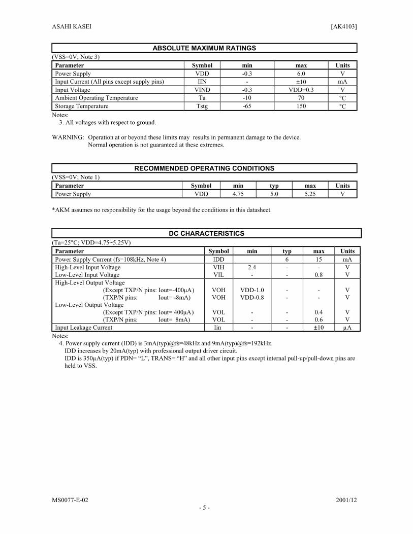
ABSOLUTE MAXIMUM RATINGS (VSS=0V; Note 3)
Parameter Symbol min max Units Power Supply VDD -0.3 6.0 V
Input Current (All pins except supply pins) IIN - ±10 mA
Input Voltage VIND -0.3 VDD+0.3 V
Ambient Operating Temperature Ta -10 70 °C
Storage Temperature Tstg -65 150 °C
Notes:
3. All voltages with respect to ground.
WARNING: Operation at or beyond these limits may results in permanent damage to the device.
Normal operation is not guaranteed at these extremes.
RECOMMENDED OPERATING CONDITIONS (VSS=0V; Note 1)
Parameter Symbol min typ max Units Power Supply VDD 4.75 5.0 5.25 V
*AKM assumes no responsibility for the usage beyond the conditions in this datasheet.
DC CHARACTERISTICS (Ta=25°C; VDD=4.75~5.25V)
Parameter Symbol min typ max Units Power Supply Current (fs=108kHz, Note 4) IDD 6 15 mA
High-Level Input Voltage
Low-Level Input Voltage
VIH
VIL
2.4
-
-
-
-
0.8
V
V
High-Level Output Voltage
(Except TXP/N pins: Iout=-400µA)
(TXP/N pins: Iout= -8mA)
Low-Level Output Voltage
(Except TXP/N pins: Iout= 400µA)
(TXP/N pins: Iout= 8mA)
VOH
VOH
VOL
VOL
VDD-1.0
VDD-0.8
-
-
-
-
-
-
-
-
0.4
0.6
V
V
V
V
Input Leakage Current Iin - - ±10 µA
Notes:
4. Power supply current (IDD) is 3mA(typ)@fs=48kHz and 9mA(typ)@fs=192kHz.
IDD increases by 20mA(typ) with professional output driver circuit.
IDD is 350µA(typ) if PDN= “L”, TRANS= “H” and all other input pins except internal pull-up/pull-down pins are
held to VSS.
ASAHI KASEI [AK4103]
MS0077-E-02 2001/12
- 6 -
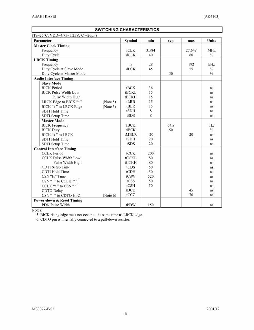
SWITCHING CHARACTERISTICS (Ta=25°C; VDD=4.75~5.25V; CL=20pF)
Parameter Symbol min typ max Units Master Clock Timing Frequency
Duty Cycle
fCLK
dCLK
3.584
40
27.648
60
MHz
%
LRCK Timing Frequency
Duty Cycle at Slave Mode
Duty Cycle at Master Mode
fs
dLCK
28
45
50
192
55
kHz
%
%
Audio Interface Timing
Slave Mode BICK Period
BICK Pulse Width Low
Pulse Width High
LRCK Edge to BICK “↑” (Note 5)
BICK “↑” to LRCK Edge (Note 5)
SDTI Hold Time
SDTI Setup Time
tBCK
tBCKL
tBCKH
tLRB
tBLR
tSDH
tSDS
36
15
15
15
15
8
8
ns
ns
ns
ns
ns
ns
ns
Master Mode
BICK Frequency
BICK Duty
BICK “↓” to LRCK
SDTI Hold Time
SDTI Setup Time
fBCK
dBCK
tMBLR
tSDH
tSDS
-20
20
20
64fs
50
20
Hz
%
ns
ns
ns
Control Interface Timing CCLK Period
CCLK Pulse Width Low
Pulse Width High
CDTI Setup Time
CDTI Hold Time
CSN “H” Time
CSN “↓” to CCLK “↑”
CCLK “↑” to CSN “↑”
CDTO Delay
CSN “↑” to CDTO Hi-Z (Note 6)
tCCK
tCCKL
tCCKH
tCDS
tCDH
tCSW
tCSS
tCSH
tDCD
tCCZ
200
80
80
50
50
520
50
50
45
70
ns
ns
ns
ns
ns
ns
ns
ns
ns
ns
Power-down & Reset Timing PDN Pulse Width
tPDW
150
ns Notes:
5. BICK rising edge must not occur at the same time as LRCK edge.
6. CDTO pin is internally connected to a pull-down resistor.
ASAHI KASEI [AK4103]
MS0077-E-02 2001/12
- 7 -
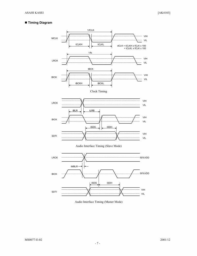
Timing Diagram
1/fCLK
tCLKL
VIH
tCLKH
MCLKVIL
dCLK = tCLKH x fCLK x 100 = tCLKL x fCLK x 100
VIHLRCK
VIL
1/fs
tBCK
tBCKL
VIH
tBCKH
BICKVIL
Clock Timing
tLRB
LRCK
VIHBICK
VIL
tSDS
VIHSDTI
VIL
tSDH
VIH
VIL
tBLR
Audio Interface Timing (Slave Mode)
LRCK
BICK
tMBLR
50%VDD
50%VDD
SDTI
tSDHtSDS
VIH
VIL
Audio Interface Timing (Master Mode)
ASAHI KASEI [AK4103]
MS0077-E-02 2001/12
- 8 -
tCCKL
CSN
CCLK
tCDS
CDTI
tCDH
tCSS
C0 *
tCCKH
CDTO Hi-Z (with pull-down resistor)
* C1
VIH
VIL
VIH
VIL
VIH
VIL
WRITE/READ Command Input Timing
tCSW
CSN
CCLK
CDTI D2 D0
tCSH
CDTO
D1D3
VIH
VIL
VIH
VIL
VIH
VIL
Hi-Z(with pull-down resistor)
WRITE Data Input Timing
CSN
CCLK
tDCD
CDTO
CDTI A1 A0
Hi-Z(with pull-downresistor)
50%VDD
VIH
VIL
VIH
VIL
VIH
VIL
D7 D6 D5
READ Data Output Timing 1
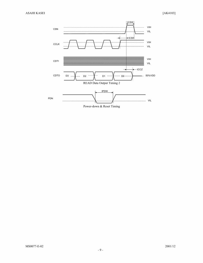
ASAHI KASEI [AK4103]
MS0077-E-02 2001/12
- 9 -
CSN
CCLK
tCCZ
CDTO D2 D1
CDTI
D0D3
tCSW
tCSH
50%VDD
VIH
VIL
VIH
VIL
VIH
VIL
READ Data Output Timing 2
tPDW
PDNVIL
Power-down & Reset Timing
ASAHI KASEI [AK4103]
MS0077-E-02 2001/12
- 10 -
OPERATION OVERVIEW
General Description
The AK4103 is a monolithic CMOS circuit that encodes and transmits audio and digital data according to the AES3,
IEC60958, S/PDIF and EIAJ CP1201 interface standards. There is one set of stereo channels that can be transmitted
simultaneously. The chip accepts audio data and control data separately, multiplexes and biphase-mark encodes the data
internally, and drives it directly or through a transformer to a transmission line. There are two modes of operation:
asynchronous and synchronous. The asynchronous mode is fully software programmable through a serial control
interface and contains buffer memory for control data. The synchronous mode has dedicated pins for the important
control bits and a serial input port for the C, U and V bits.
Initialization The AK4103 takes 8 bit clock cycles to initialize after PDN goes inactive. Also, for correct synchronization, MCLK
should be synchronized with LRCK but the phase is not critical. An internal reset will occur if the relationship between
MCLK and LRCK shifts by 3 MCLK cycles from their initial conditions.
MCLK and LRCK Relationship
For correct synchronization, MCLK and LRCK should be derived from the same clock signal either directly (as through
a frequency divider) or indirectly (for example, as through a DSP). The relationship of BICK to LRCK is fixed and
should not change. If MCLK or LRCK move such that they are shifted 3 or more MCLK cycles from their initial
conditions, the chip will generate an internal reset. After this reset, the TX outputs will transmit default values.
The following frequencies are supported for MCLK: 128fs/256fs/384fs/512fs.
CKS1 CKS0 MCLK fs
0 0 128fs 28k-192kHz
0 1 256fs 28k-108kHz
1 0 384fs 28k-54kHz
1 1 512fs 28k-54kHz
Table 1. MCLK Frequency
Asynchronous Mode/ Synchronous Mode
1. Asynchronous Mode (software controlled) The AK4103 can be configured in the asynchronous mode by connecting the ANS pin to logic “L”. In this mode the 16
to 24-bit audio samples are accepted through a configured audio serial port, and the channel status and user data through
a serial control host interface (SCI). The SCI allows access to internal buffer memory and control registers which are
used to store the channel status and user data. 4bytes per channel of user and channel status is stored. This data is
multiplexed with the audio data from the audio serial port, the parity bit is generated, and the bit stream is biphase-mark
encoded and driven through the RS422 line driver. The CRCC code for the channel status is also generated according to
the professional mode definition in the AES3 standards. This mode also allows for software control for mute, reset,
audio format selection, clock frequency settings and output enables, via the serial host interface.
ASAHI KASEI [AK4103]
MS0077-E-02 2001/12
- 11 -
2. Synchronous Mode (hardware controlled) The AK4103 when configured in synchronous mode accepts 16 - 24 bit audio samples through the audio serial port and
provides dedicated pins for the control data and allows all channel status, user data and validity bits to be serially input
through port pins. This data is multiplexed, the parity bit generated, and the bit stream is biphase-mark encoded and
driven through an RS422 line driver. The two set of channels have individual channel status and user data pins.
2-1. Audio Routing Mode (Transparent Mode) The AK4103 can be configured in audio routing mode (transparent mode) by ANS=TRANS=1. In this mode, the
channel status(C), user data(U) and validity(V) bits must pass through unaltered. The Block Start(B) signal is configured
as an input, allowing the transmit block structure to be slaved to the block structure of the receiver. The C, U and V are
now transmitted with the current audio sample. In audio routing mode, no CRC bytes are generated and C bits pass
through unaltered. In audio routing mode, the FS0/CSN pin changes definition to AKMODE pin. When set “H” the
AK4103 can be configured directly with the AK4112A receiver. When set “L”, it may be used with other non-AKM
receivers. Setting the part with TRANS=1 and ANS=0 is illegal and places the chip into a test mode.
PIN Modes
ANS TRANS Synchronous/Asynchronous Audio Routing Source for C, U and V bits
0 0 Asynchronous mode Normal mode
C Pin ORed Control Register
U Pin ORed Control Register
V Pin ORed Control Register
0 1 (Test mode)
1 0 Normal mode
1 1 Synchronous mode
Audio routing mode C,U and V pin
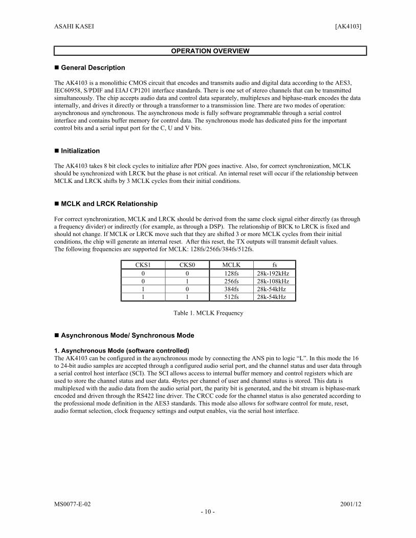
Table 2. Mode setting
BLS
C (or U,V) C(L0) C(R0) C(L1) C(R31)C(L31) C(L32)C(R191)
SDTI
LRCK (I2S)
L0 R0 L31 R31R191 L1 L32
LRCK (except I2S)
Figure 1. Audio routing mode timing (AKMODE=0)
ASAHI KASEI [AK4103]
MS0077-E-02 2001/12
- 12 -
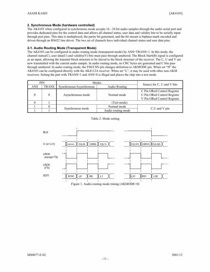
BLS
C (or U,V)
LRCK
C(L0) C(R0) C(L1) C(R31)C(L31) C(L32)C(R191)
SDTI (except I2S)
L191 R191 L0 R30 R31L31 SDTI (I2S)
L191 R191 L30 L31R30L0R190
R0
Figure 2. Audio routing mode timing (AKMODE=1)
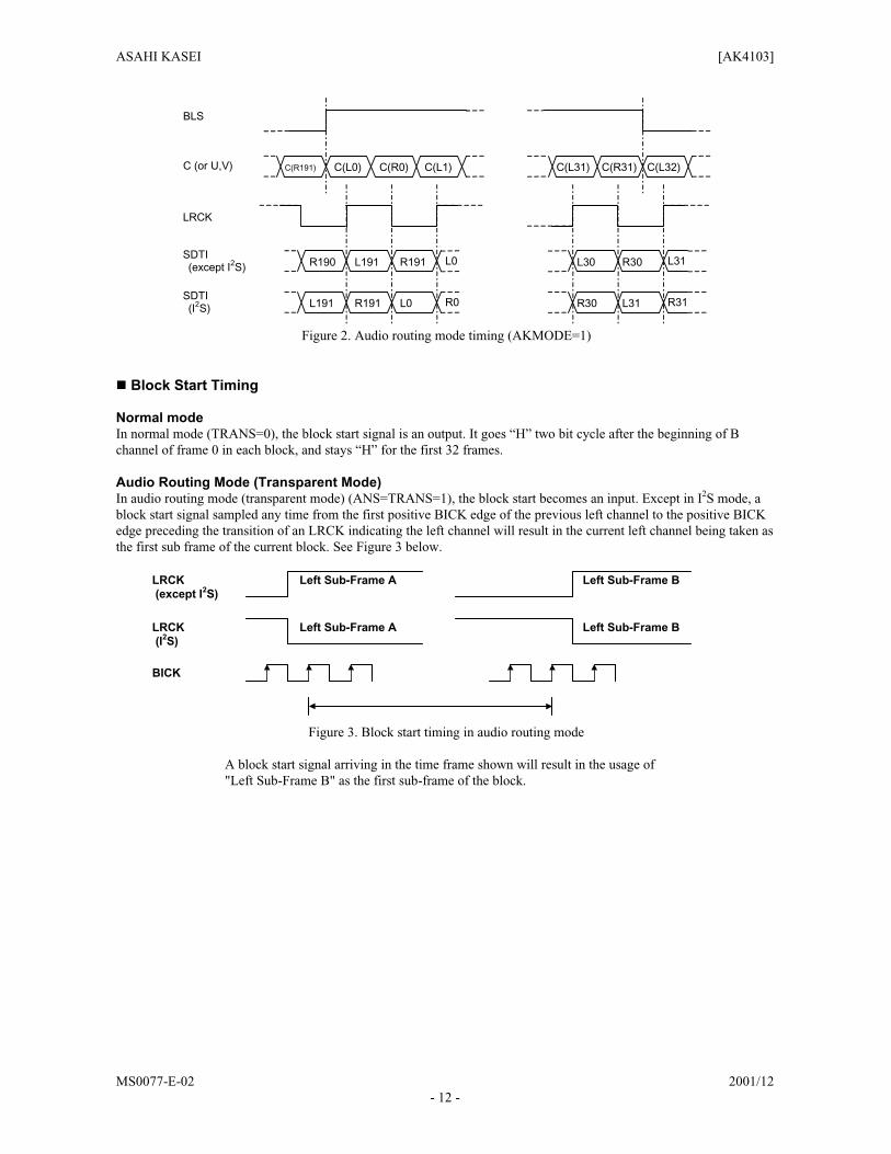
Block Start Timing Normal mode In normal mode (TRANS=0), the block start signal is an output. It goes “H” two bit cycle after the beginning of B
channel of frame 0 in each block, and stays “H” for the first 32 frames.
Audio Routing Mode (Transparent Mode) In audio routing mode (transparent mode) (ANS=TRANS=1), the block start becomes an input. Except in I
2S mode, a
block start signal sampled any time from the first positive BICK edge of the previous left channel to the positive BICK
edge preceding the transition of an LRCK indicating the left channel will result in the current left channel being taken as
the first sub frame of the current block. See Figure 3 below.
BICK
LRCK (except I2S)
Left Sub-Frame A Left Sub-Frame B
LRCK (I2S)
Left Sub-Frame A Left Sub-Frame B
Figure 3. Block start timing in audio routing mode
A block start signal arriving in the time frame shown will result in the usage of
"Left Sub-Frame B" as the first sub-frame of the block.
ASAHI KASEI [AK4103]
MS0077-E-02 2001/12
- 13 -
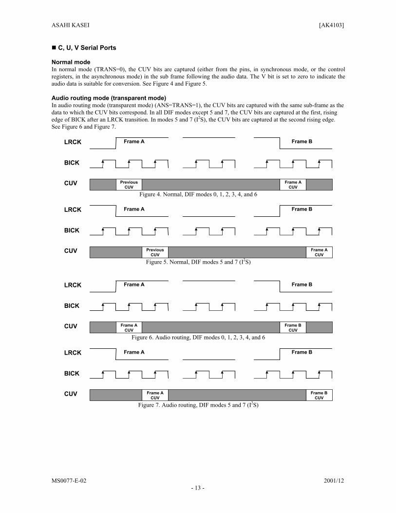
C, U, V Serial Ports Normal mode In normal mode (TRANS=0), the CUV bits are captured (either from the pins, in synchronous mode, or the control
registers, in the asynchronous mode) in the sub frame following the audio data. The V bit is set to zero to indicate the
audio data is suitable for conversion. See Figure 4 and Figure 5.
Audio routing mode (transparent mode) In audio routing mode (transparent mode) (ANS=TRANS=1), the CUV bits are captured with the same sub-frame as the
data to which the CUV bits correspond. In all DIF modes except 5 and 7, the CUV bits are captured at the first, rising
edge of BICK after an LRCK transition. In modes 5 and 7 (I2S), the CUV bits are captured at the second rising edge.
See Figure 6 and Figure 7.
CUV
BICK
LRCK
PreviousCUV
Frame A Frame B
Frame ACUV
Figure 4. Normal, DIF modes 0, 1, 2, 3, 4, and 6
CUV
BICK
LRCK
PreviousCUV
Frame A Frame B
Frame ACUV
Figure 5. Normal, DIF modes 5 and 7 (I2S)
CUV
BICK
LRCK
Frame ACUV
Frame A Frame B
Frame BCUV
Figure 6. Audio routing, DIF modes 0, 1, 2, 3, 4, and 6
CUV
BICK
LRCK
Frame ACUV
Frame A Frame B
Frame BCUV
Figure 7. Audio routing, DIF modes 5 and 7 (I2S)
ASAHI KASEI [AK4103]
MS0077-E-02 2001/12
- 14 -
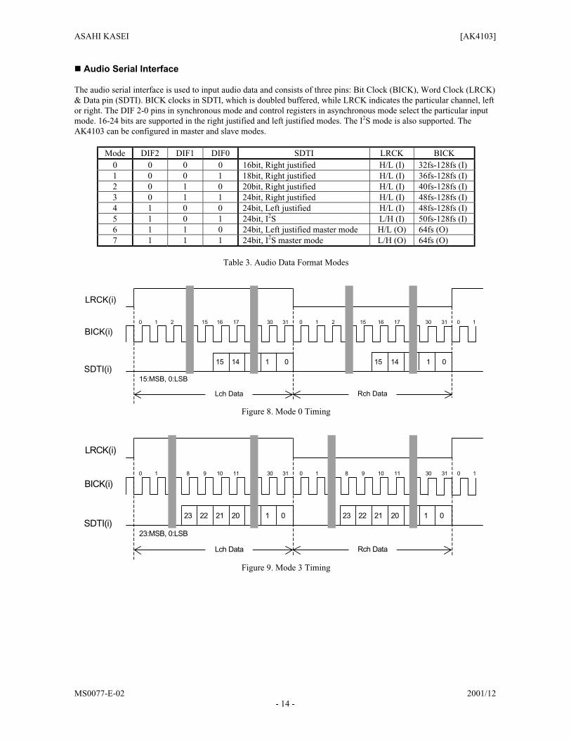
Audio Serial Interface
The audio serial interface is used to input audio data and consists of three pins: Bit Clock (BICK), Word Clock (LRCK)
& Data pin (SDTI). BICK clocks in SDTI, which is doubled buffered, while LRCK indicates the particular channel, left
or right. The DIF 2-0 pins in synchronous mode and control registers in asynchronous mode select the particular input
mode. 16-24 bits are supported in the right justified and left justified modes. The I2S mode is also supported. The
AK4103 can be configured in master and slave modes.
Mode DIF2 DIF1 DIF0 SDTI LRCK BICK
0 0 0 0 16bit, Right justified H/L (I) 32fs-128fs (I)
1 0 0 1 18bit, Right justified H/L (I) 36fs-128fs (I)
2 0 1 0 20bit, Right justified H/L (I) 40fs-128fs (I)
3 0 1 1 24bit, Right justified H/L (I) 48fs-128fs (I)
4 1 0 0 24bit, Left justified H/L (I) 48fs-128fs (I)
5 1 0 1 24bit, I2S L/H (I) 50fs-128fs (I)
6 1 1 0 24bit, Left justified master mode H/L (O) 64fs (O)
7 1 1 1 24bit, I2S master mode L/H (O) 64fs (O)
Table 3. Audio Data Format Modes
LRCK(i)
BICK(i)
SDTI(i)
0 1 2 31 0 1
15:MSB, 0:LSB
Lch Data Rch Data
15 1716 1531 0 1 2 1716
0 1 01
30
15 141415
30
Figure 8. Mode 0 Timing
LRCK(i)
BICK(i)
SDTI(i)
0 1 8 31 0 1
23:MSB, 0:LSB
Lch Data Rch Data
9 1110 931 0 1 8 1110
0 1 01
30
21 202021
30
2223 2223
Figure 9. Mode 3 Timing
ASAHI KASEI [AK4103]
MS0077-E-02 2001/12
- 15 -
LRCK
BICK
SDTI(i)
0 1 2 31 0 1
23:MSB, 0:LSB
Lch Data Rch Data
21 2322 2131 0 1 2 2322
23 222
30
1 001
30
212223 21 2 23 22
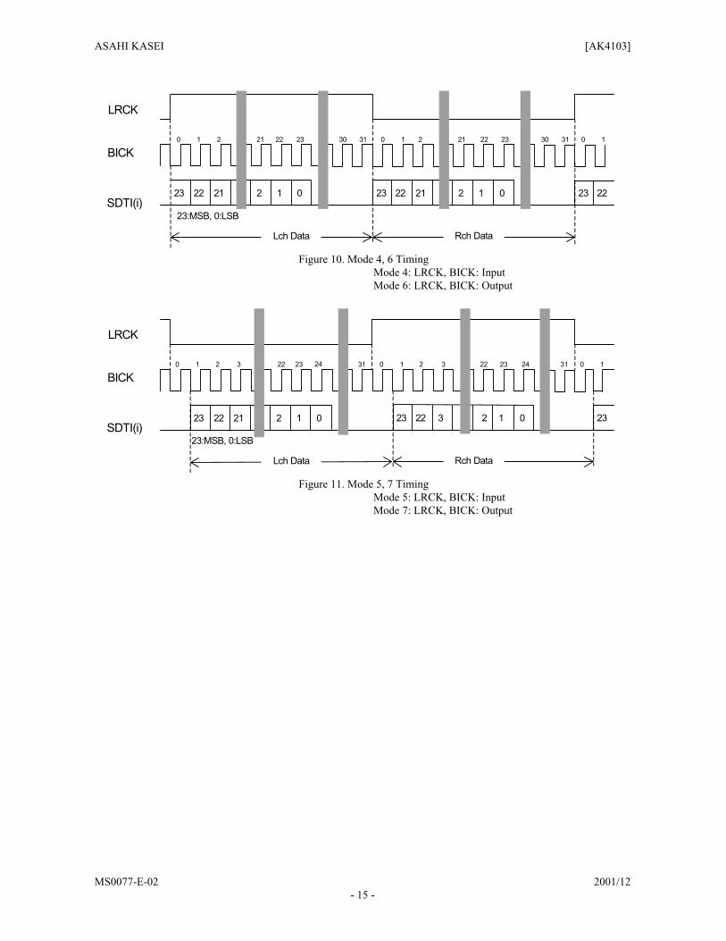
Figure 10. Mode 4, 6 Timing
Mode 4: LRCK, BICK: Input
Mode 6: LRCK, BICK: Output
LRCK
BICK
SDTI(i)
0 1 2 31 0 1
23:MSB, 0:LSB
Lch Data Rch Data
233 231 0 1 233
23 22
24
1 0
24
3 2 23
22
2 01212223
22
Figure 11. Mode 5, 7 Timing
Mode 5: LRCK, BICK: Input
Mode 7: LRCK, BICK: Output
ASAHI KASEI [AK4103]
MS0077-E-02 2001/12
- 16 -
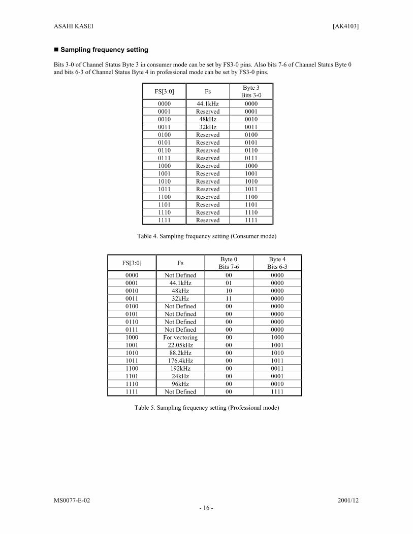
Sampling frequency setting Bits 3-0 of Channel Status Byte 3 in consumer mode can be set by FS3-0 pins. Also bits 7-6 of Channel Status Byte 0
and bits 6-3 of Channel Status Byte 4 in professional mode can be set by FS3-0 pins.
FS[3:0] Fs Byte 3
Bits 3-0
0000 44.1kHz 0000
0001 Reserved 0001
0010 48kHz 0010
0011 32kHz 0011
0100 Reserved 0100
0101 Reserved 0101
0110 Reserved 0110
0111 Reserved 0111
1000 Reserved 1000
1001 Reserved 1001
1010 Reserved 1010
1011 Reserved 1011
1100 Reserved 1100
1101 Reserved 1101
1110 Reserved 1110
1111 Reserved 1111
Table 4. Sampling frequency setting (Consumer mode)
FS[3:0] Fs Byte 0
Bits 7-6
Byte 4
Bits 6-3
0000 Not Defined 00 0000
0001 44.1kHz 01 0000
0010 48kHz 10 0000
0011 32kHz 11 0000
0100 Not Defined 00 0000
0101 Not Defined 00 0000
0110 Not Defined 00 0000
0111 Not Defined 00 0000
1000 For vectoring 00 1000
1001 22.05kHz 00 1001
1010 88.2kHz 00 1010
1011 176.4kHz 00 1011
1100 192kHz 00 0011
1101 24kHz 00 0001
1110 96kHz 00 0010
1111 Not Defined 00 1111
Table 5. Sampling frequency setting (Professional mode)
ASAHI KASEI [AK4103]
MS0077-E-02 2001/12
- 17 -
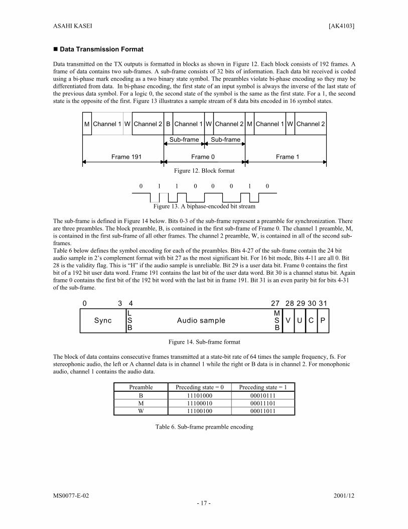
Data Transmission Format Data transmitted on the TX outputs is formatted in blocks as shown in Figure 12. Each block consists of 192 frames. A
frame of data contains two sub-frames. A sub-frame consists of 32 bits of information. Each data bit received is coded
using a bi-phase mark encoding as a two binary state symbol. The preambles violate bi-phase encoding so they may be
differentiated from data. In bi-phase encoding, the first state of an input symbol is always the inverse of the last state of
the previous data symbol. For a logic 0, the second state of the symbol is the same as the first state. For a 1, the second
state is the opposite of the first. Figure 13 illustrates a sample stream of 8 data bits encoded in 16 symbol states.
Frame 191 Frame 0 Frame 1
Sub-frame Sub-frame
M Channel 1 W Channel 2 B Channel 1 W Channel 2 M Channel 1 W Channel 2
Figure 12. Block format
0 1 1 0 0 0 1 0
Figure 13. A biphase-encoded bit stream
The sub-frame is defined in Figure 14 below. Bits 0-3 of the sub-frame represent a preamble for synchronization. There
are three preambles. The block preamble, B, is contained in the first sub-frame of Frame 0. The channel 1 preamble, M,
is contained in the first sub-frame of all other frames. The channel 2 preamble, W, is contained in all of the second sub-
frames.
Table 6 below defines the symbol encoding for each of the preambles. Bits 4-27 of the sub-frame contain the 24 bit
audio sample in 2’s complement format with bit 27 as the most significant bit. For 16 bit mode, Bits 4-11 are all 0. Bit
28 is the validity flag. This is “H” if the audio sample is unreliable. Bit 29 is a user data bit. Frame 0 contains the first
bit of a 192 bit user data word. Frame 191 contains the last bit of the user data word. Bit 30 is a channel status bit. Again
frame 0 contains the first bit of the 192 bit word with the last bit in frame 191. Bit 31 is an even parity bit for bits 4-31
of the sub-frame.
Sync PCUVL MS Audio sample SB B
0 3 4 27 28 29 30 31
Figure 14. Sub-frame format
The block of data contains consecutive frames transmitted at a state-bit rate of 64 times the sample frequency, fs. For
stereophonic audio, the left or A channel data is in channel 1 while the right or B data is in channel 2. For monophonic
audio, channel 1 contains the audio data.
Preamble Preceding state = 0 Preceding state = 1
B 11101000 00010111
M 11100010 00011101
W 11100100 00011011
Table 6. Sub-frame preamble encoding
ASAHI KASEI [AK4103]
MS0077-E-02 2001/12
- 18 -
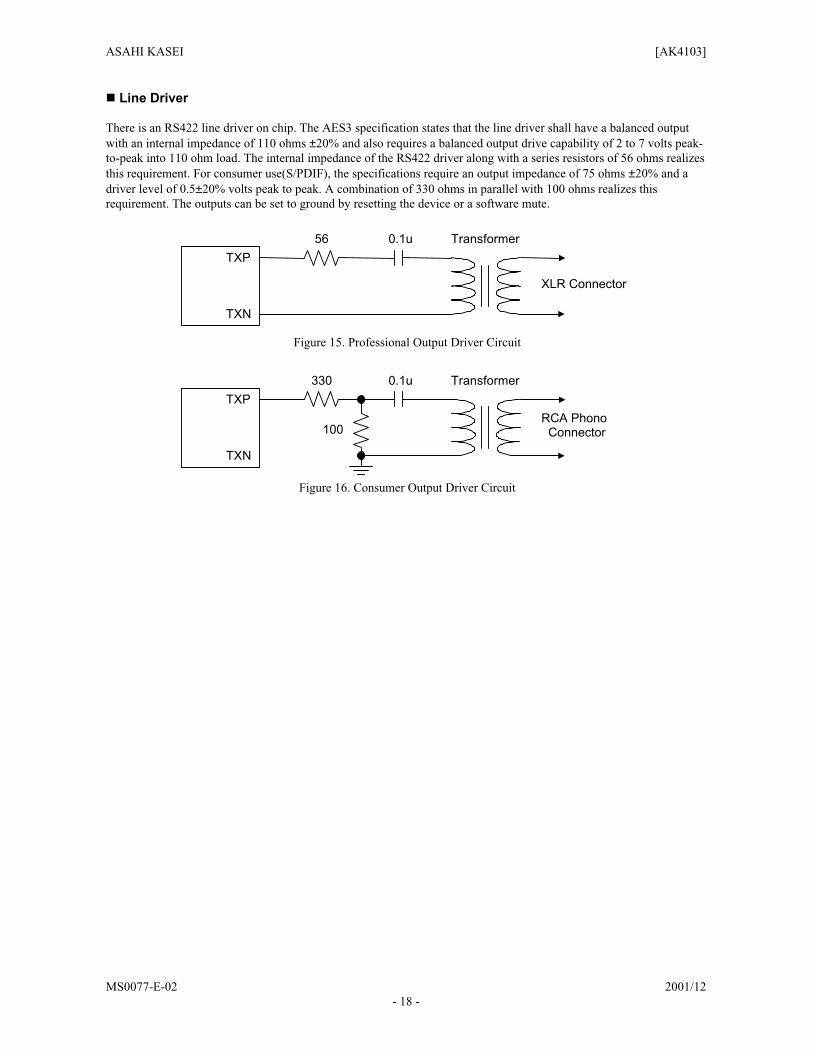
Line Driver
There is an RS422 line driver on chip. The AES3 specification states that the line driver shall have a balanced output
with an internal impedance of 110 ohms ±20% and also requires a balanced output drive capability of 2 to 7 volts peak-
to-peak into 110 ohm load. The internal impedance of the RS422 driver along with a series resistors of 56 ohms realizes
this requirement. For consumer use(S/PDIF), the specifications require an output impedance of 75 ohms ±20% and a
driver level of 0.5±20% volts peak to peak. A combination of 330 ohms in parallel with 100 ohms realizes this
requirement. The outputs can be set to ground by resetting the device or a software mute.
TXP
TXN
56 0.1u
XLR Connector
Transformer
Figure 15. Professional Output Driver Circuit
TXP
TXN
330 0.1u
RCA Phono Connector
Transformer
100
Figure 16. Consumer Output Driver Circuit
ASAHI KASEI [AK4103]
MS0077-E-02 2001/12
- 19 -
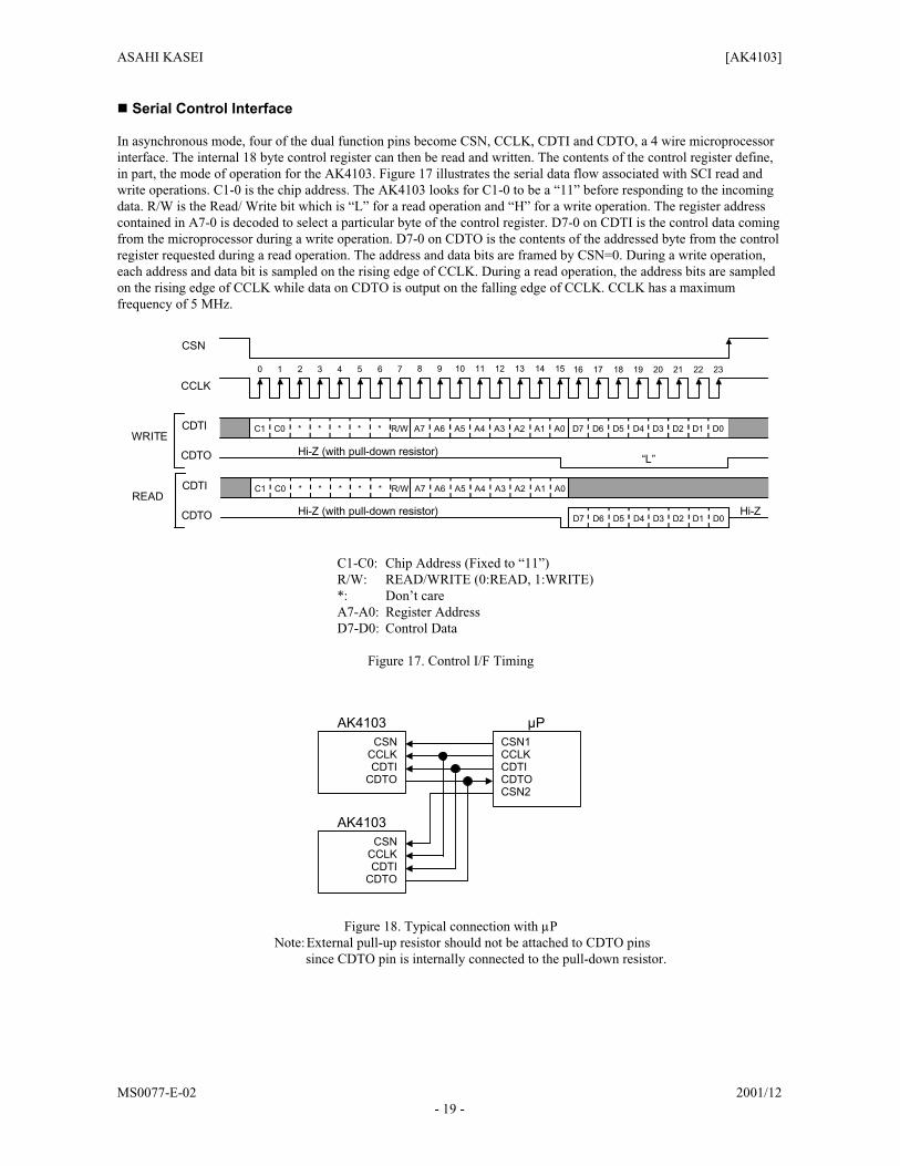
Serial Control Interface In asynchronous mode, four of the dual function pins become CSN, CCLK, CDTI and CDTO, a 4 wire microprocessor
interface. The internal 18 byte control register can then be read and written. The contents of the control register define,
in part, the mode of operation for the AK4103. Figure 17 illustrates the serial data flow associated with SCI read and
write operations. C1-0 is the chip address. The AK4103 looks for C1-0 to be a “11” before responding to the incoming
data. R/W is the Read/ Write bit which is “L” for a read operation and “H” for a write operation. The register address
contained in A7-0 is decoded to select a particular byte of the control register. D7-0 on CDTI is the control data coming
from the microprocessor during a write operation. D7-0 on CDTO is the contents of the addressed byte from the control
register requested during a read operation. The address and data bits are framed by CSN=0. During a write operation,
each address and data bit is sampled on the rising edge of CCLK. During a read operation, the address bits are sampled
on the rising edge of CCLK while data on CDTO is output on the falling edge of CCLK. CCLK has a maximum
frequency of 5 MHz.
CDTI
CCLK
CSN
C1
0 1 2 3 4 5 6 7 16 17 18 19 20 21 22 23
D4 D5 D6 D7 * * * * * C0 R/W D0 D1 D2 D3
CDTO Hi-Z (with pull-down resistor) WRITE
CDTI C1 D4 D5 D6 D7 * * * * * C0 R/W D0 D1 D2 D3
CDTO Hi-Z (with pull-down resistor) READ
D4 D5 D6 D7 D0 D1 D2 D3 Hi-Z
A7
8 9 10 11 12 13 14 15
A1 A2 A3 A4 A5 A6 A0
A7 A1 A2 A3 A4 A5 A6 A0
“L”
C1-C0: Chip Address (Fixed to “11”)
R/W: READ/WRITE (0:READ, 1:WRITE)
*: Don’t care
A7-A0: Register Address
D7-D0: Control Data
Figure 17. Control I/F Timing
CSN
AK4103
CCLKCDTI
CDTO
CSN
AK4103
CCLKCDTI
CDTO
µPCSN1CCLKCDTICDTOCSN2
Figure 18. Typical connection with µP Note: External pull-up resistor should not be attached to CDTO pins
since CDTO pin is internally connected to the pull-down resistor.
ASAHI KASEI [AK4103]
MS0077-E-02 2001/12
- 20 -
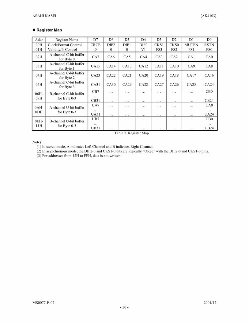
Register Map
Addr Register Name D7 D6 D5 D4 D3 D2 D1 D0
00H Clock/Format Control CRCE DIF2 DIF1 DIF0 CKS1 CKS0 MUTEN RSTN
01H Validity/fs Control 0 0 0 V1 FS3 FS2 FS1 FS0
02H A-channel C-bit buffer
for Byte 0 CA7 CA6 CA5 CA4 CA3 CA2 CA1 CA0
03H A-channel C-bit buffer
for Byte 1 CA15 CA14 CA13 CA12 CA11 CA10 CA9 CA8
04H A-channel C-bit buffer
for Byte 2 CA23 CA22 CA21 CA20 CA19 CA18 CA17 CA16
05H A-channel C-bit buffer
for Byte 3 CA31 CA30 CA29 CA28 CA27 CA26 CA25 CA24
06H-
09H
B-channel C-bit buffer
for Byte 0-3
CB7
…
CB31
…
…
…
…
…
…
…
…
…
…
…
…
CB0
…
CB24
0AH-
0DH
A-channel U-bit buffer
for Byte 0-3
UA7
…
UA31
…
…
…
…
…
…
…
…
…
…
…
…
UA0
…
UA24
0EH-
11H
B-channel U-bit buffer
for Byte 0-3
UB7
…
UB31
…
…
…
…
…
…
…
…
…
…
…
…
UB0
…
UB24
Table 7. Register Map
Notes:
(1) In stereo mode, A indicates Left Channel and B indicates Right Channel.
(2) In asynchronous mode, the DIF2-0 and CKS1-0 bits are logically “ORed” with the DIF2-0 and CKS1-0 pins.
(3) For addresses from 12H to FFH, data is not written.
ASAHI KASEI [AK4103]
MS0077-E-02 2001/12
- 21 -
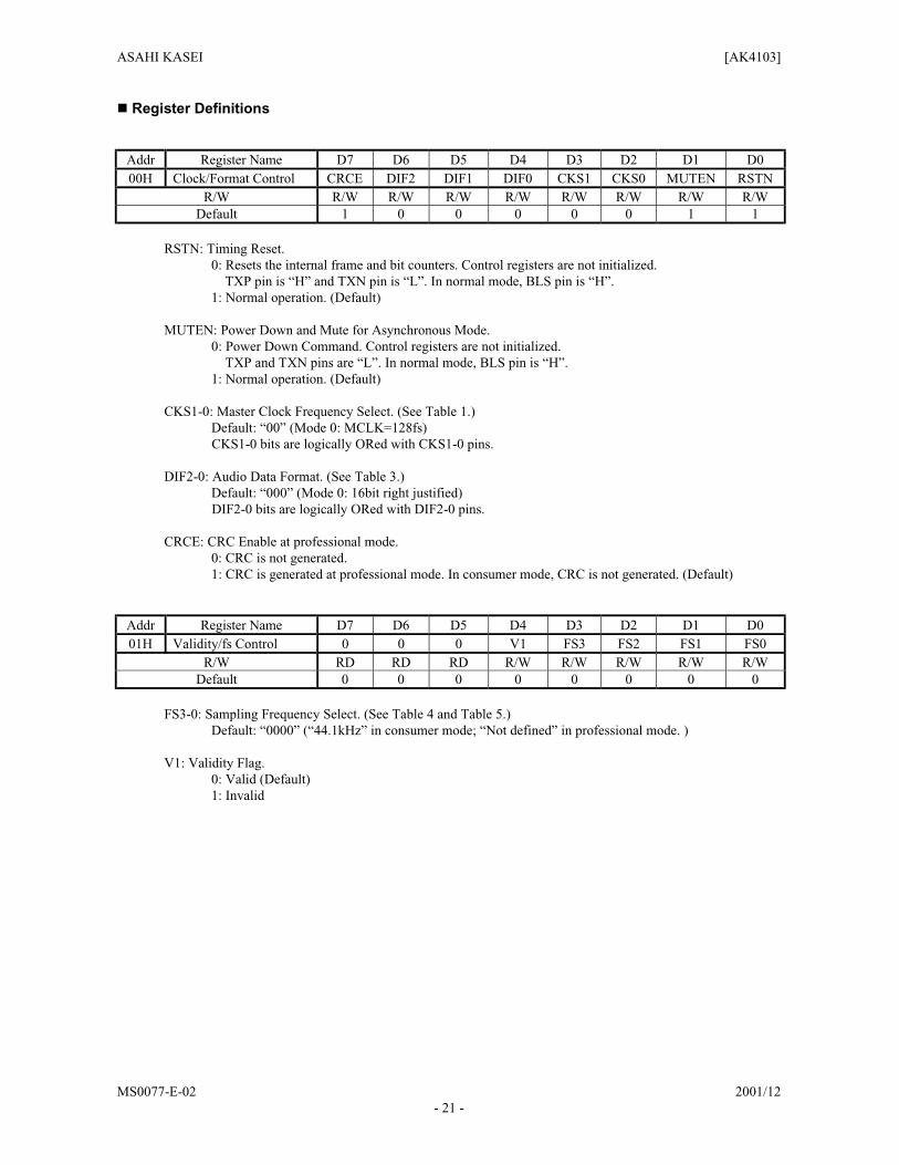
Register Definitions
Addr Register Name D7 D6 D5 D4 D3 D2 D1 D0
00H Clock/Format Control CRCE DIF2 DIF1 DIF0 CKS1 CKS0 MUTEN RSTN
R/W R/W R/W R/W R/W R/W R/W R/W R/W
Default 1 0 0 0 0 0 1 1
RSTN: Timing Reset.
0: Resets the internal frame and bit counters. Control registers are not initialized.
TXP pin is “H” and TXN pin is “L”. In normal mode, BLS pin is “H”.
1: Normal operation. (Default)
MUTEN: Power Down and Mute for Asynchronous Mode.
0: Power Down Command. Control registers are not initialized.
TXP and TXN pins are “L”. In normal mode, BLS pin is “H”.
1: Normal operation. (Default)
CKS1-0: Master Clock Frequency Select. (See Table 1.)
Default: “00” (Mode 0: MCLK=128fs)
CKS1-0 bits are logically ORed with CKS1-0 pins.
DIF2-0: Audio Data Format. (See Table 3.)
Default: “000” (Mode 0: 16bit right justified)
DIF2-0 bits are logically ORed with DIF2-0 pins.
CRCE: CRC Enable at professional mode.
0: CRC is not generated.
1: CRC is generated at professional mode. In consumer mode, CRC is not generated. (Default)
Addr Register Name D7 D6 D5 D4 D3 D2 D1 D0
01H Validity/fs Control 0 0 0 V1 FS3 FS2 FS1 FS0
R/W RD RD RD R/W R/W R/W R/W R/W
Default 0 0 0 0 0 0 0 0
FS3-0: Sampling Frequency Select. (See Table 4 and Table 5.)
Default: “0000” (“44.1kHz” in consumer mode; “Not defined” in professional mode. )
V1: Validity Flag.
0: Valid (Default)
1: Invalid
ASAHI KASEI [AK4103]
MS0077-E-02 2001/12
- 22 -
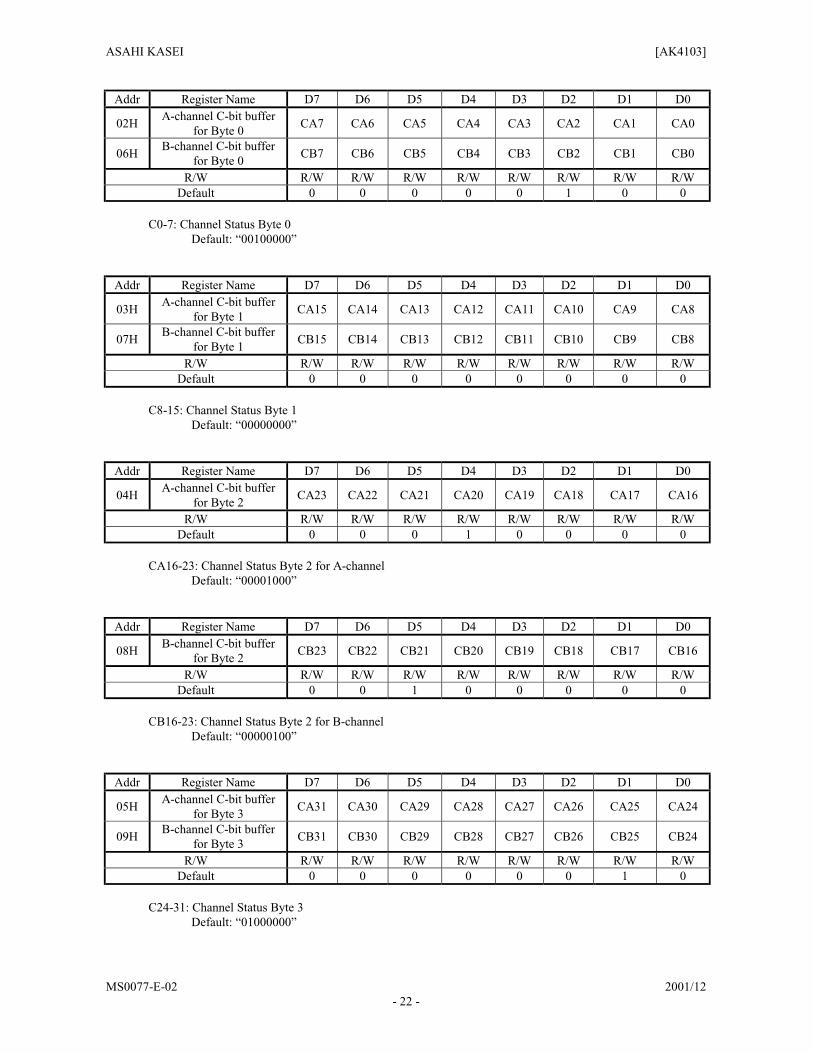
Addr Register Name D7 D6 D5 D4 D3 D2 D1 D0
02H A-channel C-bit buffer
for Byte 0 CA7 CA6 CA5 CA4 CA3 CA2 CA1 CA0
06H B-channel C-bit buffer
for Byte 0 CB7 CB6 CB5 CB4 CB3 CB2 CB1 CB0
R/W R/W R/W R/W R/W R/W R/W R/W R/W
Default 0 0 0 0 0 1 0 0
C0-7: Channel Status Byte 0
Default: “00100000”
Addr Register Name D7 D6 D5 D4 D3 D2 D1 D0
03H A-channel C-bit buffer
for Byte 1 CA15 CA14 CA13 CA12 CA11 CA10 CA9 CA8
07H B-channel C-bit buffer
for Byte 1 CB15 CB14 CB13 CB12 CB11 CB10 CB9 CB8
R/W R/W R/W R/W R/W R/W R/W R/W R/W
Default 0 0 0 0 0 0 0 0
C8-15: Channel Status Byte 1
Default: “00000000”
Addr Register Name D7 D6 D5 D4 D3 D2 D1 D0
04H A-channel C-bit buffer
for Byte 2 CA23 CA22 CA21 CA20 CA19 CA18 CA17 CA16
R/W R/W R/W R/W R/W R/W R/W R/W R/W
Default 0 0 0 1 0 0 0 0
CA16-23: Channel Status Byte 2 for A-channel
Default: “00001000”
Addr Register Name D7 D6 D5 D4 D3 D2 D1 D0
08H B-channel C-bit buffer
for Byte 2 CB23 CB22 CB21 CB20 CB19 CB18 CB17 CB16
R/W R/W R/W R/W R/W R/W R/W R/W R/W
Default 0 0 1 0 0 0 0 0
CB16-23: Channel Status Byte 2 for B-channel
Default: “00000100”
Addr Register Name D7 D6 D5 D4 D3 D2 D1 D0
05H A-channel C-bit buffer
for Byte 3 CA31 CA30 CA29 CA28 CA27 CA26 CA25 CA24
09H B-channel C-bit buffer
for Byte 3 CB31 CB30 CB29 CB28 CB27 CB26 CB25 CB24
R/W R/W R/W R/W R/W R/W R/W R/W R/W
Default 0 0 0 0 0 0 1 0
C24-31: Channel Status Byte 3
Default: “01000000”
ASAHI KASEI [AK4103]
MS0077-E-02 2001/12
- 23 -
Addr Register Name D7 D6 D5 D4 D3 D2 D1 D0
0AH-
0DH
A-channel U-bit buffer
for Byte 0-3
UA7
…
UA31
…
…
…
…
…
…
…
…
…
…
…
…
UA0
…
UA24
0EH-
11H
B-channel U-bit buffer
for Byte 0-3
UB7
…
UB31
…
…
…
…
…
…
…
…
…
…
…
…
UB0
…
UB24
R/W R/W R/W R/W R/W R/W R/W R/W R/W
Default 0 0 0 0 0 0 0 0
U0-31: User Data
Default: all “0” Default values of control registers
Bits Default
CRCE 1 CRC is generated.
DIF2-0 000 16bit, Right justified
CKS1-0 00 MCLK=128fs
V1 0 Valid data
FS3-0 0000 fs=44.1kHz
MUTEN 1 Normal Operation
RSTN 1 Normal Operation
Channel Status
- Bit0 0 Consumer Mode
- Bit1 0 Audio Mode
- Bit2 1 No Copyright
- Bit3-5 000 No Emphasis
Byte0
- Bit6-7 00 Mode 0
Byte1 - Bit0-7 00000000 General Category Code
- Bit0-3 0000 Source Number: Don’t care Byte2
- Bit4-7 1000
0100
Channel A Source channel
Channel B Source channel
- Bit0-3 0100 fs=48kHz
- Bit4-5 00 Standard Clock Accuracy
Byte3
- Bit6-7 00
User Data All zeros
Table 8. Default Values of Control Register
ASAHI KASEI [AK4103]
MS0077-E-02 2001/12
- 24 -
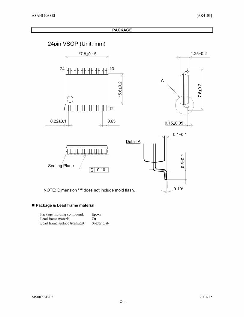
PACKAGE
0.1±0.1
0-10°
Detail A
Seating Plane
NOTE: Dimension "*" does not include mold flash.
0.10
0.15±0.050.22±0.1 0.65
*7.8±0.15 1.25±0.2
A
1 12
1324
24pin VSOP (Unit: mm)
7.6 ±
0.2
0.5 ±
0.2
*5.6
±0.2
Package & Lead frame material
Package molding compound: Epoxy
Lead frame material: Cu
Lead frame surface treatment: Solder plate
ASAHI KASEI [AK4103]
MS0077-E-02 2001/12
- 25 -
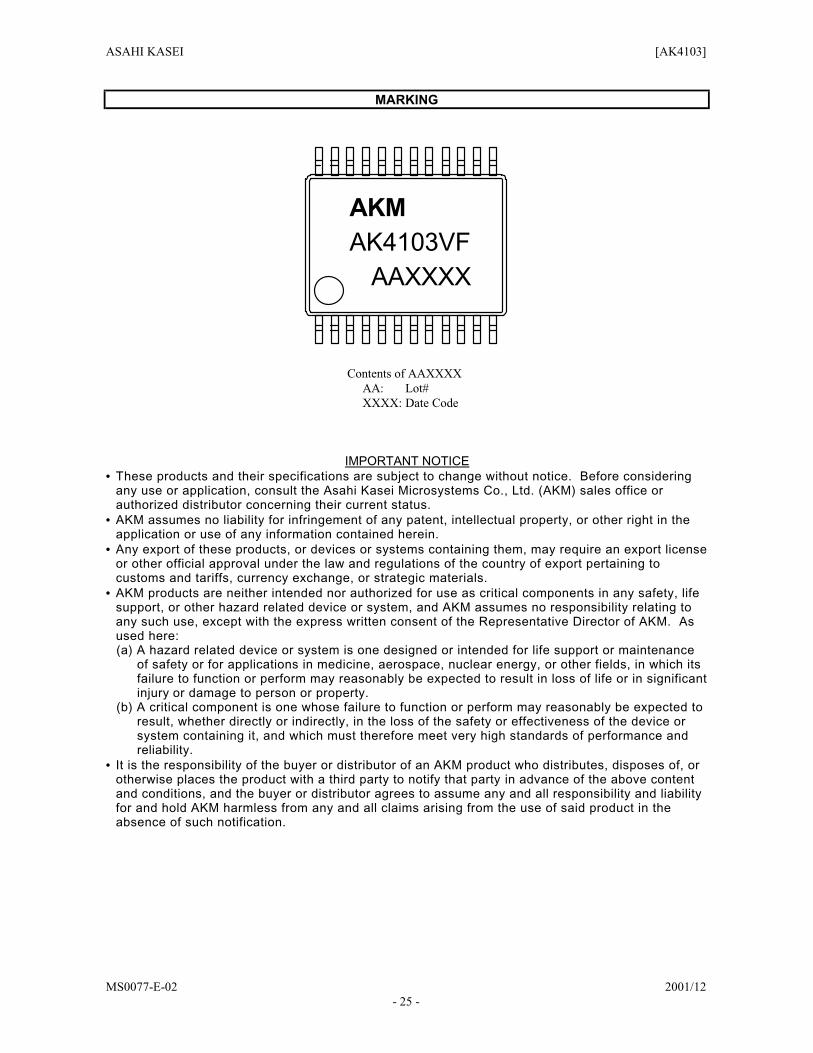
MARKING
AKMAK4103VF
AAXXXX
Contents of AAXXXX
AA: Lot#
XXXX: Date Code
IMPORTANT NOTICE
• These products and their specifications are subject to change without notice. Before considering any use or application, consult the Asahi Kasei Microsystems Co., Ltd. (AKM) sales office or authorized distributor concerning their current status.
• AKM assumes no liability for infringement of any patent, intellectual property, or other right in the application or use of any information contained herein.
• Any export of these products, or devices or systems containing them, may require an export license or other official approval under the law and regulations of the country of export pertaining to customs and tariffs, currency exchange, or strategic materials.
• AKM products are neither intended nor authorized for use as critical components in any safety, life support, or other hazard related device or system, and AKM assumes no responsibility relating to any such use, except with the express written consent of the Representative Director of AKM. As used here: (a) A hazard related device or system is one designed or intended for life support or maintenance
of safety or for applications in medicine, aerospace, nuclear energy, or other fields, in which its failure to function or perform may reasonably be expected to result in loss of life or in significant injury or damage to person or property.
(b) A critical component is one whose failure to function or perform may reasonably be expected to result, whether directly or indirectly, in the loss of the safety or effectiveness of the device or system containing it, and which must therefore meet very high standards of performance and reliability.
• It is the responsibility of the buyer or distributor of an AKM product who distributes, disposes of, or otherwise places the product with a third party to notify that party in advance of the above content and conditions, and the buyer or distributor agrees to assume any and all responsibility and liability for and hold AKM harmless from any and all claims arising from the use of said product in the absence of such notification.