Embed Size (px)
Citation preview
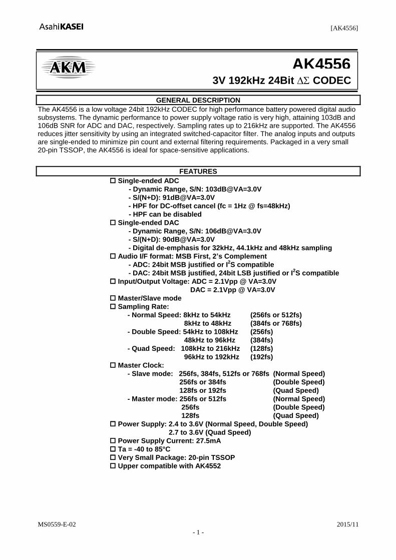
[AK4556]
MS0559-E-02 2015/11
- 1 -
GENERAL DESCRIPTION
The AK4556 is a low voltage 24bit 192kHz CODEC for high performance battery powered digital audio subsystems. The dynamic performance to power supply voltage ratio is very high, attaining 103dB and 106dB SNR for ADC and DAC, respectively. Sampling rates up to 216kHz are supported. The AK4556 reduces jitter sensitivity by using an integrated switched-capacitor filter. The analog inputs and outputs are single-ended to minimize pin count and external filtering requirements. Packaged in a very small 20-pin TSSOP, the AK4556 is ideal for space-sensitive applications.
FEATURES
Single-ended ADC
- Dynamic Range, S/N: 103dB@VA=3.0V
- S/(N+D): 91dB@VA=3.0V
- HPF for DC-offset cancel (fc = 1Hz @ fs=48kHz)
- HPF can be disabled
Single-ended DAC
- Dynamic Range, S/N: 106dB@VA=3.0V
- S/(N+D): 90dB@VA=3.0V
- Digital de-emphasis for 32kHz, 44.1kHz and 48kHz sampling
Audio I/F format: MSB First, 2’s Complement
- ADC: 24bit MSB justified or I2S compatible
- DAC: 24bit MSB justified, 24bit LSB justified or I2S compatible
Input/Output Voltage: ADC = 2.1Vpp @ VA=3.0V
DAC = 2.1Vpp @ VA=3.0V
Master/Slave mode
Sampling Rate:
- Normal Speed: 8kHz to 54kHz (256fs or 512fs)
8kHz to 48kHz (384fs or 768fs)
- Double Speed: 54kHz to 108kHz (256fs)
48kHz to 96kHz (384fs)
- Quad Speed: 108kHz to 216kHz (128fs)
96kHz to 192kHz (192fs)
Master Clock:
- Slave mode: 256fs, 384fs, 512fs or 768fs (Normal Speed)
256fs or 384fs (Double Speed)
128fs or 192fs (Quad Speed)
- Master mode: 256fs or 512fs (Normal Speed)
256fs (Double Speed)
128fs (Quad Speed)
Power Supply: 2.4 to 3.6V (Normal Speed, Double Speed)
2.7 to 3.6V (Quad Speed)
Power Supply Current: 27.5mA
Ta = -40 to 85°C
Very Small Package: 20-pin TSSOP
Upper compatible with AK4552
3V 192kHz 24Bit CODEC
AK4556
[AK4556]
MS0559-E-02 2015/11
- 2 -
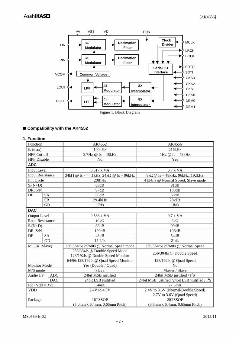
Modulator
MCLK
VA VSS
LOUT
LIN
LRCK
BCLK
VCOM
RIN
Modulator
Decimation
Filter
Serial I/O
Interface Common Voltage
SDTO
Decimation
Filter
SDTI
CKS3
Clock
Divider
ROUT
8X
Interpolator
8X
Interpolator
Modulator
Modulator
PDN
LPF
LPF
CKS2
VD
CKS1
CKS0
DEM0
DEM1
Figure 1. Block Diagram
■ Compatibility with the AK4552
1. Function
Function AK4552 AK4556
fs (max) 100kHz 216kHz
HFP Cut-off 3.7Hz @ fs = 48kHz 1Hz @ fs = 48kHz
HPF Disable No Yes
ADC
Input Level 0.617 x VA 0.7 x VA
Input Resistance 34k @ fs = 44.1kHz, 24k @ fs = 96kHz 8k@ fs = 48kHz, 96kHz, 192kHz
Init Cycle 2081/fs 4134/fs @ Normal Speed, Slave mode
S/(N+D) 89dB 91dB
DR, S/N 97dB 103dB
DF SA 65dB 68dB
SB 29.4kHz 28kHz
GD 17/fs 18/fs
DAC
Output Level 0.583 x VA 0.7 x VA
Road Resistance 10k 5k
S/(N+D) 88dB 90dB
DR, S/N 100dB 106dB
DF SA 43dB 54dB
GD 15.4/fs 21/fs
MCLK (Slave) 256/384/512/768fs @ Normal Speed mode 256/384/512/768fs @ Normal Speed
256/384fs @ Double Speed Mode
128/192fs @ Double Speed Monitor 256/384fs @ Double Speed
64/96/128/192fs @ Quad Speed Monitor 128/192fs @ Quad Speed
Monitor Mode Yes (Double / Quad) No
M/S mode Slave Master / Slave
Audio I/F ADC 24bit MSB justified 24bit MSB justified / I2S
DAC 24bit LSB justified 24bit MSB justified /24bit LSB justified / I2S
Idd (Vdd = 3V) 14mA 27.5mA
VDD 2.4V to 4.0V 2.4V to 3.6V (Normal/Double Speed)
2.7V to 3.6V (Quad Speed)
Package 16TSSOP
(5.0mm x 6.4mm, 0.65mm Pitch)
20TSSOP
(6.5mm x 6.4mm, 0.65mm Pitch)
[AK4556]
MS0559-E-02 2015/11
- 3 -
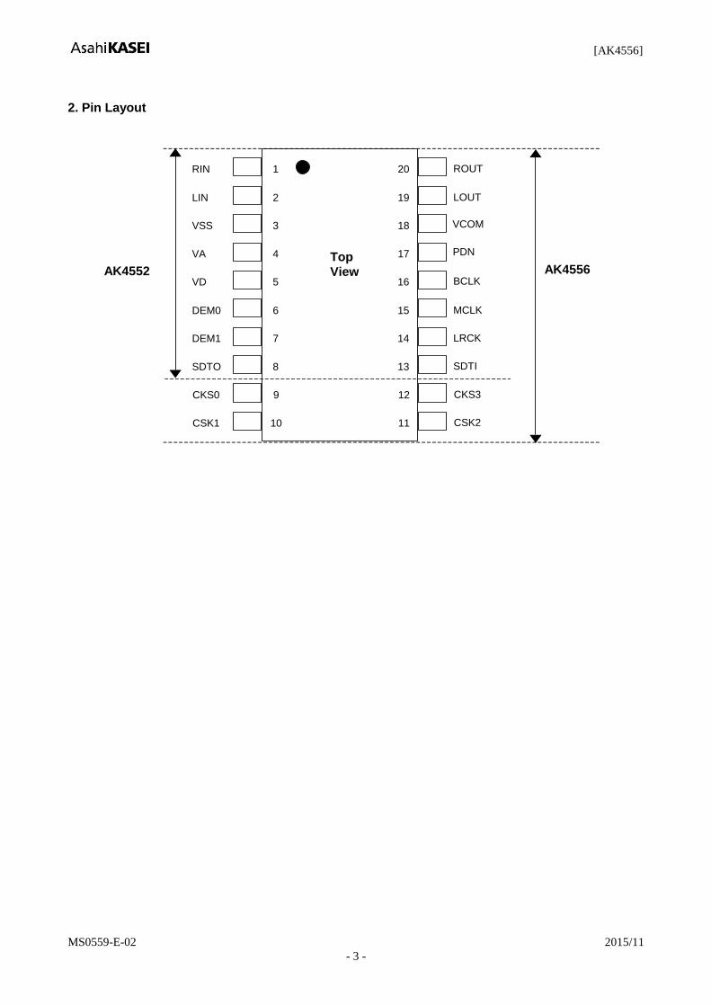
2. Pin Layout
1 RIN
LIN
VA
VSS
VD
DEM0
DEM1
SDTO
Top
View
2
3
4
5
6
7
8
ROUT
LOUT
PDN
BCLK
MCLK
LRCK
SDTI
20
19
18
17
16
15
14
13
VCOM
CKS0
CSK1
9
10
CKS3
CSK2
12
11
AK4552 AK4556
[AK4556]
MS0559-E-02 2015/11
- 4 -
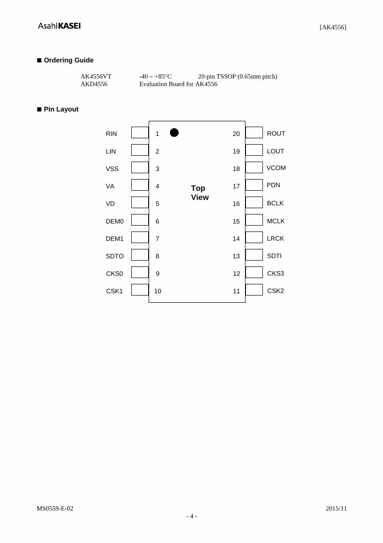
■ Ordering Guide
AK4556VT -40 +85C 20-pin TSSOP (0.65mm pitch)
AKD4556 Evaluation Board for AK4556
■ Pin Layout
1 RIN
LIN
VA
VSS
VD
DEM0
DEM1
SDTO
Top
View
2
3
4
5
6
7
8
ROUT
LOUT
PDN
BCLK
MCLK
LRCK
SDTI
20
19
18
17
16
15
14
13
VCOM
CKS0
CSK1
9
10
CKS3
CSK2
12
11
[AK4556]
MS0559-E-02 2015/11
- 5 -
PIN/FUNCTION
No. Pin Name I/O Function
1 RIN I Rch Analog Input Pin
2 LIN I Lch Analog Input Pin
3 VSS - Ground Pin
4 VA - Analog Power Supply Pin
5 VD - Digital Power Supply Pin
6 DEM0 I De-emphasis Control Pin
7 DEM1 I De-emphasis Control Pin
8 SDTO O Audio Serial Data Output Pin
When PDN pin is “L”, SDTO pin outputs “L”.
9 CKS0 I Mode Setting Pin #0
10 CSK1 I Mode Setting Pin #1
11 CSK2 I Mode Setting Pin #2
12 CSK3 I Mode Setting Pin #3
13 SDTI I Audio Serial Data Input Pin
14 LRCK I/O Input/Output Channel Clock Pin
When PDN pin is “L”, LRCK pin outputs “L” in master mode.
15 MCLK I Master Clock Input Pin
16 BCLK I/O Audio Serial Data Clock Pin
When PDN pin is “L”, BCLK pin outputs “L” in master mode.
17 PDN I
Power-Down & Reset Mode Pin
“L”: Power-down and Reset, “H”: Normal operation
The AK4556 should be reset once by bringing PDN pin = “L”.
18 VCOM O Common Voltage Output Pin, 0.5 x VA
19 LOUT O Lch Analog Output Pin
When PDN pin is “L”, LOUT pin becomes Hi-Z.
20 ROUT O Rch Analog Output Pin
When PDN pin is “L”, ROUT pin becomes Hi-Z.
Note: Do not allow digital input pins except analog input pins (LIN and RIN) to float.
■ Handling of Unused Pin
The unused I/O pin should be processed appropriately as below.
Classification Pin Name Setting
Analog Input LIN, RIN These pins should be open.
Analog Output LOUT, ROUT These pins should be open.
[AK4556]
MS0559-E-02 2015/11
- 6 -
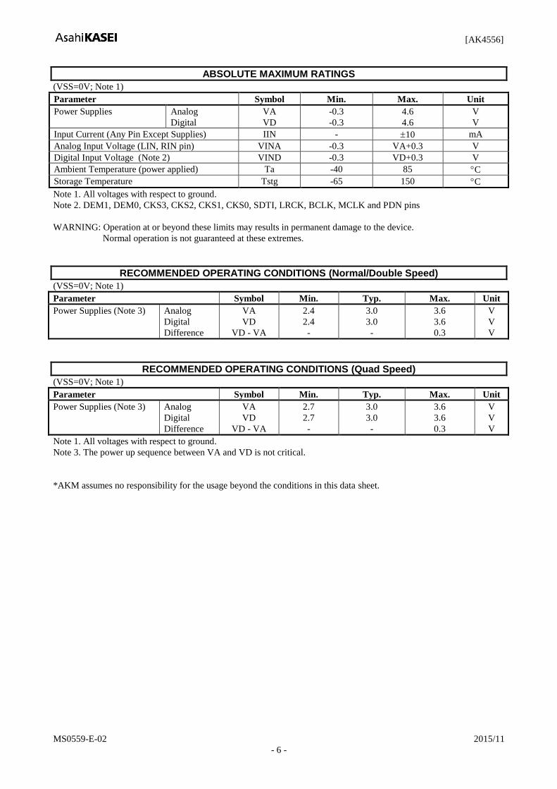
ABSOLUTE MAXIMUM RATINGS
(VSS=0V; Note 1)
Parameter Symbol Min. Max. Unit
Power Supplies
Analog
Digital
VA
VD
-0.3
-0.3
4.6
4.6
V
V
Input Current (Any Pin Except Supplies) IIN - 10 mA
Analog Input Voltage (LIN, RIN pin) VINA -0.3 VA+0.3 V
Digital Input Voltage (Note 2) VIND -0.3 VD+0.3 V
Ambient Temperature (power applied) Ta -40 85 C
Storage Temperature Tstg -65 150 C
Note 1. All voltages with respect to ground.
Note 2. DEM1, DEM0, CKS3, CKS2, CKS1, CKS0, SDTI, LRCK, BCLK, MCLK and PDN pins
WARNING: Operation at or beyond these limits may results in permanent damage to the device.
Normal operation is not guaranteed at these extremes.
RECOMMENDED OPERATING CONDITIONS (Normal/Double Speed)
(VSS=0V; Note 1)
Parameter Symbol Min. Typ. Max. Unit
Power Supplies (Note 3)
Analog
Digital
Difference
VA
VD
VD - VA
2.4
2.4
-
3.0
3.0
-
3.6
3.6
0.3
V
V
V
RECOMMENDED OPERATING CONDITIONS (Quad Speed)
(VSS=0V; Note 1)
Parameter Symbol Min. Typ. Max. Unit
Power Supplies (Note 3)
Analog
Digital
Difference
VA
VD
VD - VA
2.7
2.7
-
3.0
3.0
-
3.6
3.6
0.3
V
V
V
Note 1. All voltages with respect to ground.
Note 3. The power up sequence between VA and VD is not critical.
*AKM assumes no responsibility for the usage beyond the conditions in this data sheet.
[AK4556]
MS0559-E-02 2015/11
- 7 -
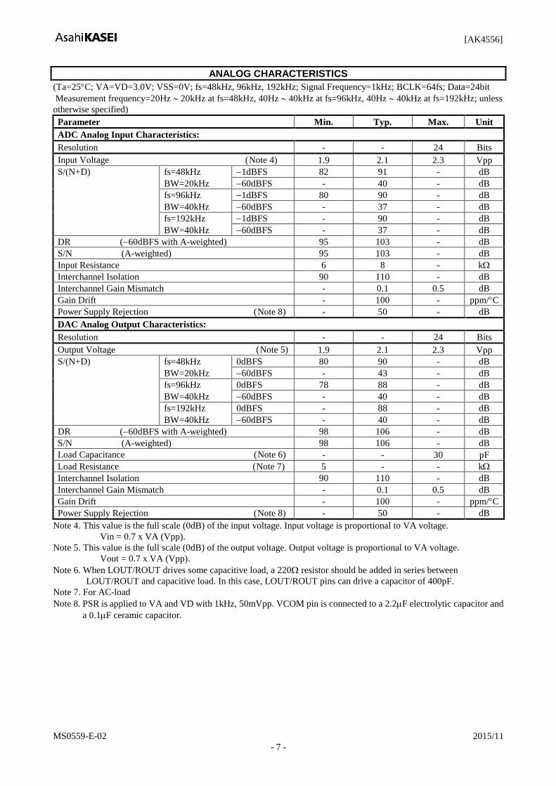
ANALOG CHARACTERISTICS
(Ta=25C; VA=VD=3.0V; VSS=0V; fs=48kHz, 96kHz, 192kHz; Signal Frequency=1kHz; BCLK=64fs; Data=24bit
Measurement frequency=20Hz 20kHz at fs=48kHz, 40Hz 40kHz at fs=96kHz, 40Hz 40kHz at fs=192kHz; unless
otherwise specified)
Parameter Min. Typ. Max. Unit
ADC Analog Input Characteristics:
Resolution - - 24 Bits
Input Voltage (Note 4) 1.9 2.1 2.3 Vpp
S/(N+D)
fs=48kHz 1dBFS 82 91 - dB
BW=20kHz 60dBFS - 40 - dB
fs=96kHz 1dBFS 80 90 - dB
BW=40kHz 60dBFS - 37 - dB
fs=192kHz 1dBFS - 90 - dB
BW=40kHz 60dBFS - 37 - dB
DR (60dBFS with A-weighted) 95 103 - dB
S/N (A-weighted) 95 103 - dB
Input Resistance 6 8 - k
Interchannel Isolation 90 110 - dB
Interchannel Gain Mismatch - 0.1 0.5 dB
Gain Drift - 100 - ppm/C
Power Supply Rejection (Note 8) - 50 - dB
DAC Analog Output Characteristics:
Resolution - - 24 Bits
Output Voltage (Note 5) 1.9 2.1 2.3 Vpp
S/(N+D)
fs=48kHz 0dBFS 80 90 - dB
BW=20kHz 60dBFS - 43 - dB
fs=96kHz 0dBFS 78 88 - dB
BW=40kHz 60dBFS - 40 - dB
fs=192kHz 0dBFS - 88 - dB
BW=40kHz 60dBFS - 40 - dB
DR (60dBFS with A-weighted) 98 106 - dB
S/N (A-weighted) 98 106 - dB
Load Capacitance (Note 6) - - 30 pF
Load Resistance (Note 7) 5 - - k
Interchannel Isolation 90 110 - dB
Interchannel Gain Mismatch - 0.1 0.5 dB
Gain Drift - 100 - ppm/C
Power Supply Rejection (Note 8) - 50 - dB
Note 4. This value is the full scale (0dB) of the input voltage. Input voltage is proportional to VA voltage.
Vin = 0.7 x VA (Vpp).
Note 5. This value is the full scale (0dB) of the output voltage. Output voltage is proportional to VA voltage.
Vout = 0.7 x VA (Vpp).
Note 6. When LOUT/ROUT drives some capacitive load, a 220 resistor should be added in series between
LOUT/ROUT and capacitive load. In this case, LOUT/ROUT pins can drive a capacitor of 400pF.
Note 7. For AC-load
Note 8. PSR is applied to VA and VD with 1kHz, 50mVpp. VCOM pin is connected to a 2.2F electrolytic capacitor and
a 0.1F ceramic capacitor.
[AK4556]
MS0559-E-02 2015/11
- 8 -
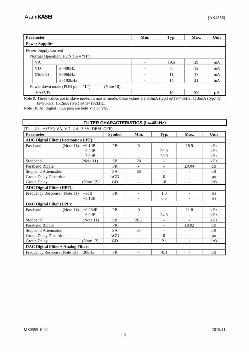
Parameter Min. Typ. Max. Unit
Power Supplies
Power Supply Current
Normal Operation (PDN pin = “H”)
VA - 19.5 29 mA
VD fs=48kHz - 8 12 mA
(Note 9) fs=96kHz - 11 17 mA
fs=192kHz - 14 21 mA
Power down mode (PDN pin = “L”) (Note 10)
VA+VD - 10 100 A
Note 9. These values are in slave mode. In master mode, these values are 8.3mA (typ.) @ fs=48kHz, 11.6mA (typ.) @
fs=96kHz, 15.2mA (typ.) @ fs=192kHz.
Note 10. All digital input pins are held VD or VSS.
FILTER CHARACTERISTICS (fs=48kHz)
(Ta= -40 +85C; VA, VD=2.4 3.6V; DEM=OFF)
Parameter Symbol Min. Typ. Max. Unit
ADC Digital Filter (Decimation LPF):
Passband (Note 11)
0.1dB
0.2dB
3.0dB
PB
0
-
-
-
20.0
23.0
18.9
-
-
kHz
kHz
kHz
Stopband (Note 11) SB 28 - - kHz
Passband Ripple PR - - 0.04 dB
Stopband Attenuation SA 68 - - dB
Group Delay Distortion GD - 0 - s
Group Delay (Note 12) GD - 18 - 1/fs
ADC Digital Filter (HPF):
Frequency Response (Note 11)
3dB
0.1dB
FR
-
-
1.0
6.5
-
-
Hz
Hz
DAC Digital Filter (LPF):
Passband (Note 11)
0.06dB
6.0dB
PB
0
-
-
24.0
21.8
-
kHz
kHz
Stopband (Note 11) SB 26.2 - - kHz
Passband Ripple PR - 0.02 dB
Stopband Attenuation SA 54 - - dB
Group Delay Distortion GD - 0 - s
Group Delay (Note 12) GD - 21 - 1/fs
DAC Digital Filter + Analog Filter:
Frequency Response (Note 13) 20kHz FR - -0.1 - dB
[AK4556]
MS0559-E-02 2015/11
- 9 -
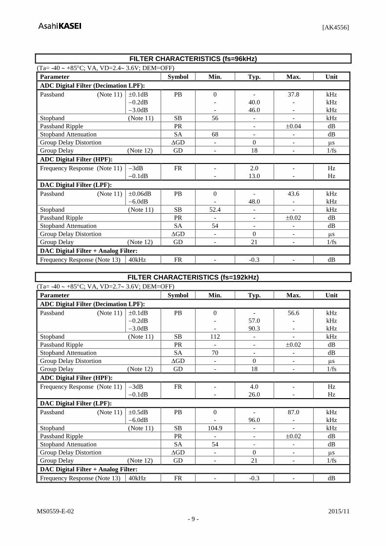
FILTER CHARACTERISTICS (fs=96kHz)
(Ta= -40 +85C; VA, VD=2.4 3.6V; DEM=OFF)
Parameter Symbol Min. Typ. Max. Unit
ADC Digital Filter (Decimation LPF):
Passband (Note 11)
0.1dB
0.2dB
3.0dB
PB
0
-
-
-
40.0
46.0
37.8
-
-
kHz
kHz
kHz
Stopband (Note 11) SB 56 - - kHz
Passband Ripple PR - 0.04 dB
Stopband Attenuation SA 68 - - dB
Group Delay Distortion GD - 0 - s
Group Delay (Note 12) GD - 18 - 1/fs
ADC Digital Filter (HPF):
Frequency Response (Note 11)
3dB
0.1dB
FR
-
-
2.0
13.0
-
-
Hz
Hz
DAC Digital Filter (LPF):
Passband (Note 11)
0.06dB
6.0dB
PB
0
-
-
48.0
43.6
-
kHz
kHz
Stopband (Note 11) SB 52.4 - - kHz
Passband Ripple PR - - 0.02 dB
Stopband Attenuation SA 54 - - dB
Group Delay Distortion GD - 0 - s
Group Delay (Note 12) GD - 21 - 1/fs
DAC Digital Filter + Analog Filter:
Frequency Response (Note 13) 40kHz FR - -0.3 - dB
FILTER CHARACTERISTICS (fs=192kHz)
(Ta= -40 +85C; VA, VD=2.7 3.6V; DEM=OFF)
Parameter Symbol Min. Typ. Max. Unit
ADC Digital Filter (Decimation LPF):
Passband (Note 11)
0.1dB
0.2dB
3.0dB
PB
0
-
-
-
57.0
90.3
56.6
-
-
kHz
kHz
kHz
Stopband (Note 11) SB 112 - - kHz
Passband Ripple PR - - 0.02 dB
Stopband Attenuation SA 70 - - dB
Group Delay Distortion GD - 0 - s
Group Delay (Note 12) GD - 18 - 1/fs
ADC Digital Filter (HPF):
Frequency Response (Note 11)
3dB
0.1dB
FR
-
-
4.0
26.0
-
-
Hz
Hz
DAC Digital Filter (LPF):
Passband (Note 11)
0.5dB
6.0dB
PB
0
-
-
96.0
87.0
-
kHz
kHz
Stopband (Note 11) SB 104.9 - - kHz
Passband Ripple PR - - 0.02 dB
Stopband Attenuation SA 54 - - dB
Group Delay Distortion GD - 0 - s
Group Delay (Note 12) GD - 21 - 1/fs
DAC Digital Filter + Analog Filter:
Frequency Response (Note 13) 40kHz FR - -0.3 - dB
[AK4556]
MS0559-E-02 2015/11
- 10 -
Note 11. The passband and stopband frequencies scales with fs (sampling frequency). For example, ADC: Passband
(0.1dB) = 0.39375 x fs (@ fs=48kHz), DAC: Passband (0.06dB) = 0.45412 x fs.
Note 12. The calculated delay time resulting from digital filtering. For the ADC, this time is from the input of an analog
signal to the setting of 24bit data for both channels to the ADC output register. For the DAC, this time is from
setting the 24 bit data both channels at the input register to the output of an analog signal.
Note 13. The reference frequency is 1kHz.
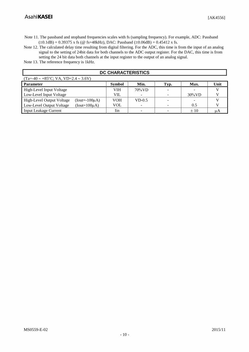
DC CHARACTERISTICS
(Ta=-40 +85C; VA, VD=2.4 3.6V)
Parameter Symbol Min. Typ. Max. Unit
High-Level Input Voltage
Low-Level Input Voltage
VIH
VIL
70VD
-
-
-
-
30VD
V
V
High-Level Output Voltage (Iout=-100A)
Low-Level Output Voltage (Iout=100A)
VOH
VOL
VD-0.5
-
-
-
-
0.5
V
V
Input Leakage Current Iin - - 10 A
[AK4556]
MS0559-E-02 2015/11
- 11 -
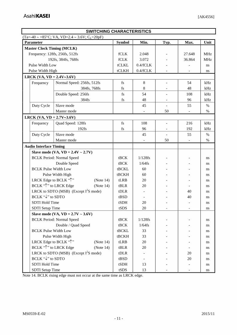
SWITCHING CHARACTERISTICS
(Ta=-40 +85C; VA, VD=2.4 3.6V; CL=20pF)
Parameter Symbol Min. Typ. Max. Unit
Master Clock Timing (MCLK)
Frequency: 128fs, 256fs, 512fs
192fs, 384fs, 768fs
Pulse Width Low
Pulse Width High
fCLK
fCLK
tCLKL
tCLKH
2.048
3.072
0.4/fCLK
0.4/fCLK
-
-
-
-
27.648
36.864
-
-
MHz
MHz
ns
ns
LRCK (VA, VD = 2.4V3.6V)
Frequency
Normal Speed: 256fs, 512fs
384fs, 768fs
fs
fs
8
8
-
-
54
48
kHz
kHz
Double Speed: 256fs
384fs
fs
fs
54
48
-
-
108
96
kHz
kHz
Duty Cycle
Slave mode
Master mode
45
-
-
50
55
-
%
%
LRCK (VA, VD = 2.7V3.6V)
Frequency
Quad Speed: 128fs
192fs
fs
fs
108
96
-
-
216
192
kHz
kHz
Duty Cycle
Slave mode
Master mode
45
-
-
50
55
-
%
%
Audio Interface Timing
Slave mode (VA, VD = 2.4V 2.7V)
BCLK Period: Normal Speed
Double Speed
BCLK Pulse Width Low
Pulse Width High
LRCK Edge to BCLK “” (Note 14)
BCLK “” to LRCK Edge (Note 14)
LRCK to SDTO (MSB) (Except I2S mode)
BCLK “” to SDTO
SDTI Hold Time
SDTI Setup Time
tBCK
tBCK
tBCKL
tBCKH
tLRB
tBLR
tDLR
tBSD
tSDH
tSDS
1/128fs
1/64fs
60
60
20
20
-
-
20
20
-
-
-
-
-
-
-
-
-
-
-
-
-
-
-
-
40
40
-
-
ns
ns
ns
ns
ns
ns
ns
ns
ns
ns
Slave mode (VA, VD = 2.7V 3.6V)
BCLK Period: Normal Speed
Double / Quad Speed
BCLK Pulse Width Low
Pulse Width High
LRCK Edge to BCLK “” (Note 14)
BCLK “” to LRCK Edge (Note 14)
LRCK to SDTO (MSB) (Except I2S mode)
BCLK “” to SDTO
SDTI Hold Time
SDTI Setup Time
tBCK
tBCK
tBCKL
tBCKH
tLRB
tBLR
tDLR
tBSD
tSDH
tSDS
1/128fs
1/64fs
33
33
20
20
-
-
13
13
-
-
-
-
-
-
-
-
-
-
-
-
-
-
-
-
20
20
-
-
ns
ns
ns
ns
ns
ns
ns
ns
ns
ns
Note 14. BCLK rising edge must not occur at the same time as LRCK edge.
[AK4556]
MS0559-E-02 2015/11
- 12 -
SWITCHING CHARACTERISTICS (Continued)
(Ta=-40 +85C; VA, VD=2.4 3.6V; CL=20pF)
Parameter Symbol Min. Typ. Max. Unit
Master mode (VA, VD = 2.4V 2.7V)
BCLK Frequency
BCLK Duty
BCLK “” to LRCK
BCLK “” to SDTO
SDTI Hold Time
SDTI Setup Time
fBCK
dBCK
tMBLR
tBSD
tSDH
tSDS
-
-
20
20
20
20
64fs
50
-
-
-
-
-
-
40
40
-
-
Hz
%
ns
ns
ns
ns
Master mode (VA, VD = 2.7V 3.6V)
BCLK Frequency
BCLK Duty
BCLK “” to LRCK
BCLK “” to SDTO
SDTI Hold Time
SDTI Setup Time
fBCK
dBCK
tMBLR
tBSD
tSDH
tSDS
-
-
20
20
13
13
64fs
50
-
-
-
-
-
-
20
20
-
-
Hz
%
ns
ns
ns
ns
Reset Timing
PDN Pulse Width (Note 15)
tPW
150
-
-
ns
PDN “” to SDTO valid (Note 16)
Slave Mode Noraml Speed tPWV - 4134 - 1/fs
Double Speed tPWV - 8262 - 1/fs
Quad Speed tPWV - 16518 - 1/fs
Master Mode Normal Speed tPWV - 4131 - 1/fs
Double Speed tPWV - 8259 - 1/fs
Quad Speed tPWV - 16515 - 1/fs
Note 15. The AK4556 can be reset by bringing the PDN pin = “L”.
Note 16. This cycle is the number of LRCK rising edges from the PDN pin = “H”.
■ Timing Diagram
MCLK
1/fCLK
tCLKH tCLKL
VIHVIL
LRCK
1/fs
VIHVIL
BCLK
tBCK
VIHVIL
tBCKH tBCKL
Figure 2. Clock Timing
[AK4556]
MS0559-E-02 2015/11
- 13 -
VIH
VIH
LRCK
VIL
VIH
BCLK
tBLR
VIL
tLRB
tDLR tDBS
SDTO
VIL
50%VD
tSDS tSDH
SDTI
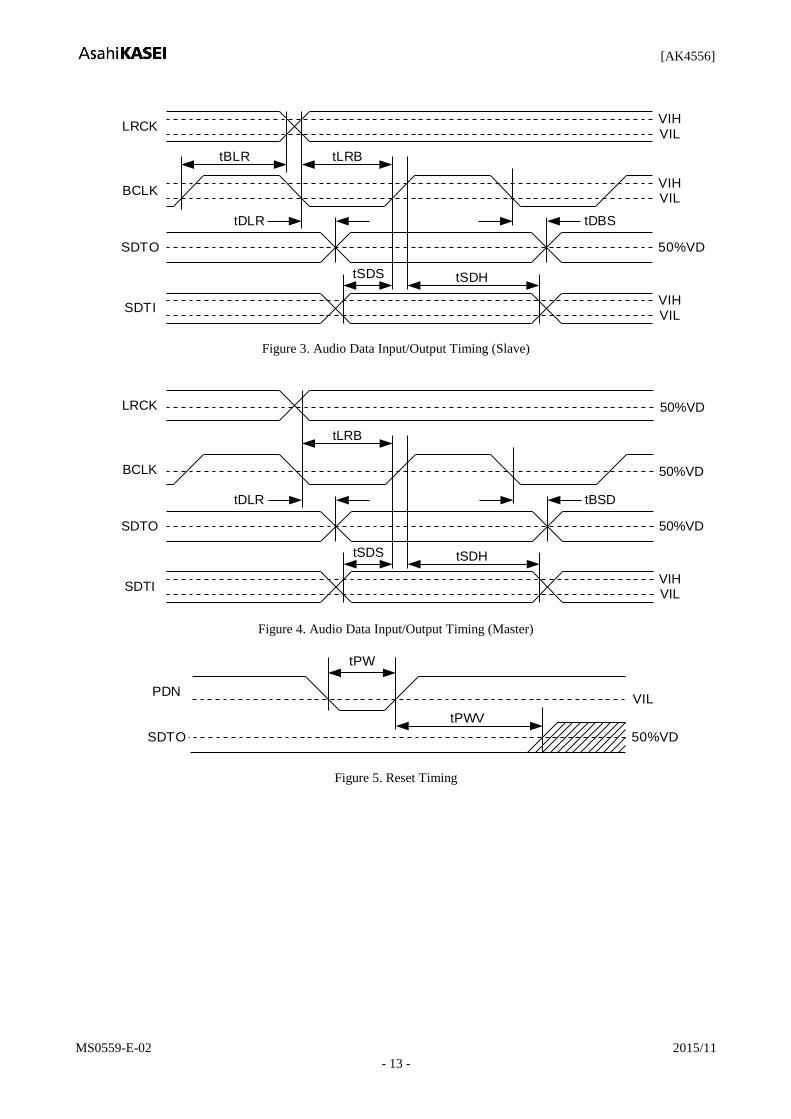
Figure 3. Audio Data Input/Output Timing (Slave)
VIH
LRCK 50%VD
BCLK
tLRB
tDLR tBSD
SDTO
VIL
50%VD
tSDS tSDH
SDTI
50%VD
Figure 4. Audio Data Input/Output Timing (Master)
PDN
SDTO
VIL
tPWV
tPW
50%VD
Figure 5. Reset Timing
[AK4556]
MS0559-E-02 2015/11
- 14 -
OPERATION OVERVIEW
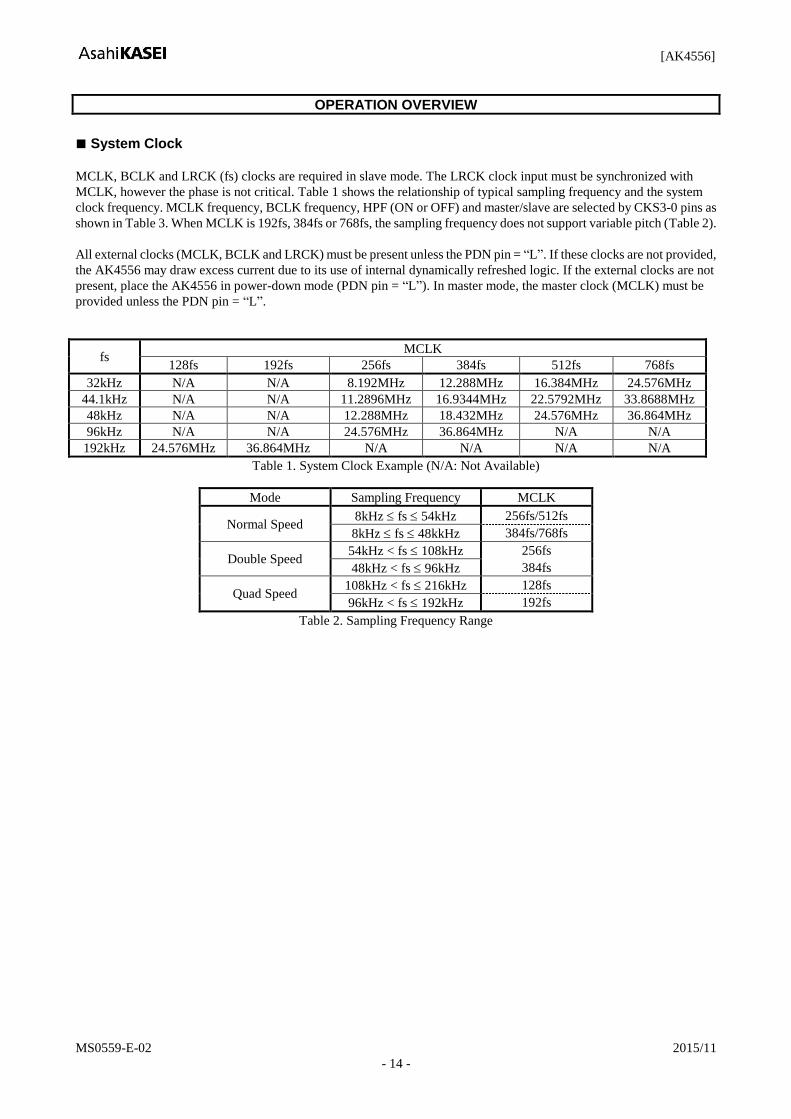
■ System Clock
MCLK, BCLK and LRCK (fs) clocks are required in slave mode. The LRCK clock input must be synchronized with
MCLK, however the phase is not critical. Table 1 shows the relationship of typical sampling frequency and the system
clock frequency. MCLK frequency, BCLK frequency, HPF (ON or OFF) and master/slave are selected by CKS3-0 pins as
shown in Table 3. When MCLK is 192fs, 384fs or 768fs, the sampling frequency does not support variable pitch (Table 2).
All external clocks (MCLK, BCLK and LRCK) must be present unless the PDN pin = “L”. If these clocks are not provided,
the AK4556 may draw excess current due to its use of internal dynamically refreshed logic. If the external clocks are not
present, place the AK4556 in power-down mode (PDN pin = “L”). In master mode, the master clock (MCLK) must be
provided unless the PDN pin = “L”.
fs MCLK
128fs 192fs 256fs 384fs 512fs 768fs
32kHz N/A N/A 8.192MHz 12.288MHz 16.384MHz 24.576MHz
44.1kHz N/A N/A 11.2896MHz 16.9344MHz 22.5792MHz 33.8688MHz
48kHz N/A N/A 12.288MHz 18.432MHz 24.576MHz 36.864MHz
96kHz N/A N/A 24.576MHz 36.864MHz N/A N/A
192kHz 24.576MHz 36.864MHz N/A N/A N/A N/A
Table 1. System Clock Example (N/A: Not Available)
Mode Sampling Frequency MCLK
Normal Speed 8kHz fs 54kHz 256fs/512fs
8kHz fs 48kkHz 384fs/768fs
Double Speed 54kHz < fs 108kHz 256fs
48kHz < fs 96kHz 384fs
Quad Speed 108kHz < fs 216kHz 128fs
96kHz < fs 192kHz 192fs
Table 2. Sampling Frequency Range
[AK4556]
MS0559-E-02 2015/11
- 15 -
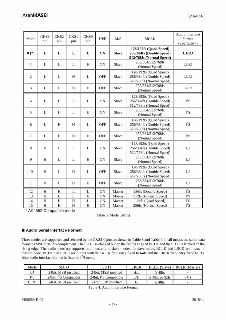
Mode CKS3
pin
CKS2
pin
CKS1
pin
CKS0
pin HPF M/S MCLK
Audio Interface
Format
(See Table 4)
0 (*) L L L L ON Slave
128/192fs (Quad Speed)
256/384fs (Double Speed)
512/768fs (Normal Speed)
LJ/RJ
1 L L L H ON Slave 256/384/512/768fs
(Normal Speed) LJ/RJ
2 L L H L OFF Slave
128/192fs (Quad Speed)
256/384fs (Double Speed)
512/768fs (Normal Speed)
LJ/RJ
3 L L H H OFF Slave 256/384/512/768fs
(Normal Speed) LJ/RJ
4 L H L L ON Slave
128/192fs (Quad Speed)
256/384fs (Double Speed)
512/768fs (Normal Speed)
I2S
5 L H L H ON Slave 256/384/512/768fs
(Normal Speed) I
2S
6 L H H L OFF Slave
128/192fs (Quad Speed)
256/384fs (Double Speed)
512/768fs (Normal Speed)
I2S
7 L H H H OFF Slave 256/384/512/768fs
(Normal Speed) I
2S
8 H L L L ON Slave
128/192fs (Quad Speed)
256/384fs (Double Speed)
512/768fs (Normal Speed)
LJ
9 H L L H ON Slave 256/384/512/768fs
(Normal Speed) LJ
10 H L H L OFF Slave
128/192fs (Quad Speed)
256/384fs (Double Speed)
512/768fs (Normal Speed)
LJ
11 H L H H OFF Slave 256/384/512/768fs
(Normal Speed) LJ
12 H H L L ON Master 256fs (Double Speed) I2S
13 H H L H ON Master 512fs (Normal Speed) I2S
14 H H H L ON Master 128fs (Quad Speed) I2S
15 H H H H ON Master 256fs (Normal Speed) I2S
* AK4552 Compatible mode
Table 3. Mode Setting
■ Audio Serial Interface Format
Three modes are supported and selected by the CKS3-0 pins as shown in Table 3 and Table 4. In all modes the serial data
format is MSB first, 2’s complement. The SDTO is clocked out on the falling edge of BCLK and the SDTI is latched on the
rising edge. The audio interface supports both master and slave modes. In slave mode, BCLK and LRCK are input. In
master mode, BCLK and LRCK are output with the BCLK frequency fixed to 64fs and the LRCK frequency fixed to 1fs.
Also audio interface format is fixed to I2S mode.
Mode SDTO SDTI LRCK BCLK (Slave) BCLK (Master)
LJ 24bit, MSB justified 24bit, MSB justified H/L 48fs -
I2S 24bit, I
2S Compatible 24bit, I
2S Compatible L/H 48fs or 32fs 64fs
LJ/RJ 24bit, MSB justified 24bit, LSB justified H/L 48fs -
Table 4. Audio Interface Format
[AK4556]
MS0559-E-02 2015/11
- 16 -
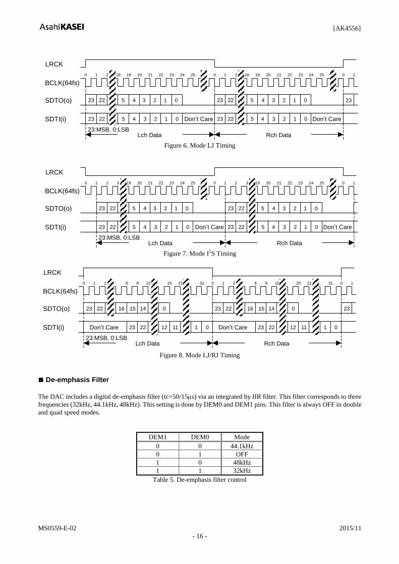
LRCK
BCLK(64fs)
SDTO(o)
0 1 2 18 19 20 21 22 0 1 2 18 19 20 22 21 0 1
SDTI(i)
23 24 25 23 24 25
23 22 4 23 22 5
4 5
4
1 22 0 23 3 2 1 22 0 23 3 2
23:MSB, 0:LSB Lch Data Rch Data
Don’t Care Don’t Care
5
5 4
1 0 3 2 1 0 3 2 23
Figure 6. Mode LJ Timing
LRCK
BCLK(64fs)
SDTO(o)
0 1 2 3 19 20 21 22 0 1 2 3 19 20 22 21 0 1
SDTI(i)
23 24 25 23 24 25
23 22 4 23 22 5
4 5
4
1 22 0 23 3 2 1 22 0 23 3 2
23:MSB, 0:LSB Lch Data Rch Data
Don’t Care Don’t Care
5
5 4
1 0 3 2 1 0 3 2
Figure 7. Mode I
2S Timing
LRCK
BCLK(64fs)
SDTO(o)
0 1 2 8 9 10 20 21 31 0 1 2 8 9 10 20 21 31 0
23
1
22 0 23 22 16 15 14 0 23
SDTI(i) 1 22 0 23 12 11 1 22 0 23 12 11
23:MSB, 0:LSB Lch Data Rch Data
Don’t Care Don’t Care
16 15 14
Figure 8. Mode LJ/RJ Timing
■ De-emphasis Filter
The DAC includes a digital de-emphasis filter (tc=50/15s) via an integrated by IIR filter. This filter corresponds to three
frequencies (32kHz, 44.1kHz, 48kHz). This setting is done by DEM0 and DEM1 pins. This filter is always OFF in double
and quad speed modes.
DEM1 DEM0 Mode
0 0 44.1kHz
0 1 OFF
1 0 48kHz
1 1 32kHz
Table 5. De-emphasis filter control
[AK4556]
MS0559-E-02 2015/11
- 17 -
■ Digital High Pass Filter
The ADC has a Digital High Pass Filter (HPF) for DC-offset cancellation. The cut-off frequency of the HPF is 1Hz at
fs=48kHz and the frequency response at 20Hz is -0.12dB. It also scales with the sampling frequency (fs). The HPF is
controlled by CKS3-0 pins (Table 3). If the HPF setting (ON/OFF) is changed at operating, click noise occurs by changing
DC offset.
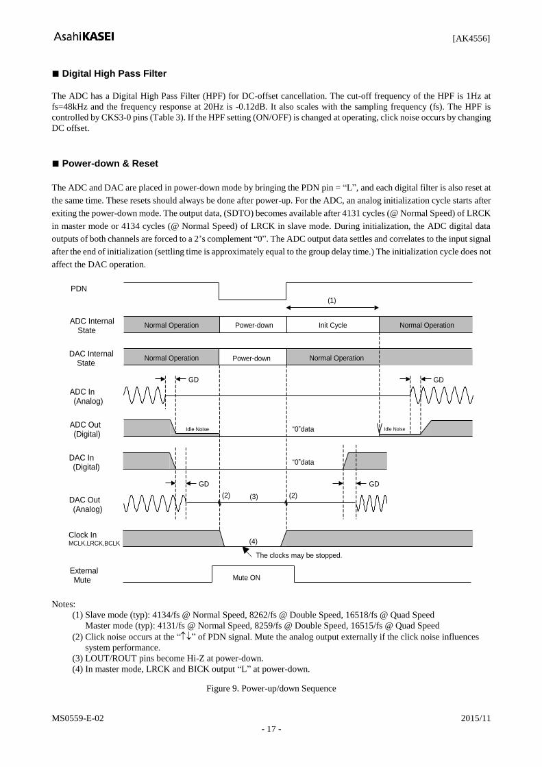
■ Power-down & Reset
The ADC and DAC are placed in power-down mode by bringing the PDN pin = “L”, and each digital filter is also reset at
the same time. These resets should always be done after power-up. For the ADC, an analog initialization cycle starts after
exiting the power-down mode. The output data, (SDTO) becomes available after 4131 cycles (@ Normal Speed) of LRCK
in master mode or 4134 cycles (@ Normal Speed) of LRCK in slave mode. During initialization, the ADC digital data
outputs of both channels are forced to a 2’s complement “0”. The ADC output data settles and correlates to the input signal
after the end of initialization (settling time is approximately equal to the group delay time.) The initialization cycle does not
affect the DAC operation.
Idle Noise
The clocks may be stopped.
ADC Internal State
PDN
(1)
Normal Operation Power-down Init Cycle Normal Operation
GD GD
Clock In MCLK,LRCK,BCLK
ADC In (Analog)
Idle Noise “0”data ADC Out (Digital)
Normal Operation Power-down Normal Operation DAC Internal State
“0”data DAC In (Digital)
DAC Out (Analog)
GD
External Mute
Mute ON
GD
(2) (2)
(4)
(3)
Notes:
(1) Slave mode (typ): 4134/fs @ Normal Speed, 8262/fs @ Double Speed, 16518/fs @ Quad Speed
Master mode (typ): 4131/fs @ Normal Speed, 8259/fs @ Double Speed, 16515/fs @ Quad Speed
(2) Click noise occurs at the “” of PDN signal. Mute the analog output externally if the click noise influences
system performance.
(3) LOUT/ROUT pins become Hi-Z at power-down.
(4) In master mode, LRCK and BICK output “L” at power-down.
Figure 9. Power-up/down Sequence
[AK4556]
MS0559-E-02 2015/11
- 18 -
■ System Reset
The AK4556 should be reset once by bringing the PDN pin “L” after power-up. In slave mode, reset and power down states
are released by MCLK and the internal timing starts clocking on the rising edge of LRCK in Mode LJ and Mode LJ/RJ. In
Mode I2S, it starts clocking on the falling edge of BCLK after the first rising edge of BCLK after the falling edge of LRCK.
The AK4556 is in power down state until LRCK is input. In master mode, reset and power down states are released by
MCLK. The internal timing also starts by MCLK.
[AK4556]
MS0559-E-02 2015/11
- 19 -
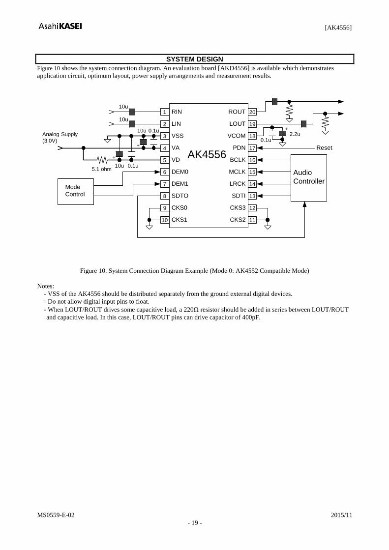
SYSTEM DESIGN
Figure 10 shows the system connection diagram. An evaluation board [AKD4556] is available which demonstrates
application circuit, optimum layout, power supply arrangements and measurement results.
AK4556
8
7
6
3
2
1
13
14
15
16
17
18
19
20
LIN
VA
VD
SDTO
RIN
SDTI
LRCK
MCLK
BCLK
PDN+
0.1u
5.1 ohm
VSS
DEM0
DEM1
Analog Supply
(3.0V)VCOM
LOUT
ROUT
10u
+
10u 0.1u
Mode
Control
Reset
0.1u2.2u
+
5
4
Audio
Controller
10
9
11
12
CKS1 CKS2
CKS3CKS0
10u
10u
Figure 10. System Connection Diagram Example (Mode 0: AK4552 Compatible Mode)
Notes:
- VSS of the AK4556 should be distributed separately from the ground external digital devices.
- Do not allow digital input pins to float.
- When LOUT/ROUT drives some capacitive load, a 220 resistor should be added in series between LOUT/ROUT
and capacitive load. In this case, LOUT/ROUT pins can drive capacitor of 400pF.
[AK4556]
MS0559-E-02 2015/11
- 20 -
1. Grounding and Power Supply Decoupling
The AK4556 requires careful attention to power supply and grounding arrangements. VA pin is usually supplied from
analog supply in system and VD pin is supplied from VA pin via 5.1. Alternatively if VA and VD pins are supplied
separately, the power up sequence is not critical. VSS pin of the AK4556 should be connected to analog ground plane.
System analog ground and digital ground should be connected together near to where the supplies are brought onto the
printed circuit board. Decoupling capacitors should be as near to the AK4556 as possible, with the small value ceramic
capacitor being the nearest.
2. Voltage Reference
The input to VA voltage sets the analog input/output range. A 0.1F ceramic capacitor and a 10F electrolytic capacitor
are connected to VA and VSS pins, normally. VCOM is a signal ground of this chip. A 2.2F electrolytic capacitor in
parallel with a 0.1F ceramic capacitor attached to these pins eliminates the effects of high frequency noise. No load
current may be drawn from VCOM pin. All signals, especially clock, should be kept away from the VA, VD and VCOM
pins in order to avoid unwanted coupling into the AK4556.
3. Analog Inputs
The ADC inputs are single-ended and internally biased to the common voltage (50%VA) with 8k (typ, @fs=48kHz,
96kHz, 192kHz) resistance. The input signal range scales with the supply voltage and nominally 0.7xVA Vpp (typ). The
ADC output data format is 2’s complement. The internal HPF removes the DC offset.
The AK4556 samples the analog inputs at 128fs (@ fs=48kHz), 64fs (@fs=96kHz) or 32fs(@192kHz). The digital filter
rejects noise above the stop band except for multiples of the sampling frequency of analog inputs. The AK4556 includes an
anti-aliasing filter (RC filter) to attenuate a noise around the sampling frequency of analog inputs.
4. Analog Outputs
The analog outputs are also single-ended and centered around the VCOM voltage. The input signal range scales with the
supply voltage and nominally 0.7 x VA Vpp (typ). The DAC input data format is 2’s complement. The output voltage is a
positive full scale for 7FFFFFH(@24bit) and a negative full scale for 800000H(@24bit). The ideal output is VCOM
voltage for 000000H(@24bit). If the noise generated by the delta-sigma modulator beyond the audio band would be the
problem, the attenuation by external filter is required.
DC offsets on analog outputs are eliminated by AC coupling since DAC outputs have DC offsets of a few mV.
[AK4556]
MS0559-E-02 2015/11
- 21 -
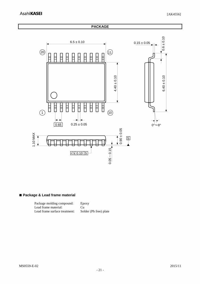
PACKAGE
20
0.0
5 ~
0.1
5
0.9
0 ±
0.0
5
1.1
0 M
AX
S
4.4
0 ±
0.1
0
0.10 S
6.5 ± 0.10
0.25 ± 0.050.65
11
101
6.4
0 ±
0.1
00
.6 ±
0.1
0
0.15 ± 0.05
0°~8°
■ Package & Lead frame material
Package molding compound: Epoxy
Lead frame material: Cu
Lead frame surface treatment: Solder (Pb free) plate
ASAHI KASEI [AK4556]
MS0559-E-02 2015/11
- 22 -
MARKING
AKM
4556VT
XXXXXXX
1) Pin #1 indication
2) Date Code: XXXXXXX (7 digits)
3) Marketing Code: 4556VT
REVISION HISTORY
Date (YY/MM/DD) Revision Reason Page Contents
06/11/06 00 First Edition
15/10/30 01 Specification
Change
21, 22 PACAGE, MARKING
Package dimension and Marking were changed.
15/11/27 02 Error
Correction
22 MARKING
“X” was added to the marking description.
ASAHI KASEI [AK4556]
MS0559-E-02 2015/11
- 23 -
IMPORTANT NOTICE
0. Asahi Kasei Microdevices Corporation (“AKM”) reserves the right to make changes to the informationcontained in this document without notice. When you consider any use or application of AKM productstipulated in this document (“Product”), please make inquiries the sales office of AKM or authorizeddistributors as to current status of the Products.
1. All information included in this document are provided only to illustrate the operation and applicationexamples of AKM Products. AKM neither makes warranties or representations with respect to theaccuracy or completeness of the information contained in this document nor grants any license to anyintellectual property rights or any other rights of AKM or any third party with respect to the information inthis document. You are fully responsible for use of such information contained in this document in yourproduct design or applications. AKM ASSUMES NO LIABILITY FOR ANY LOSSES INCURRED BYYOU OR THIRD PARTIES ARISING FROM THE USE OF SUCH INFORMATION IN YOURPRODUCT DESIGN OR APPLICATIONS.
2. The Product is neither intended nor warranted for use in equipment or systems that require extraordinarilyhigh levels of quality and/or reliability and/or a malfunction or failure of which may cause loss of humanlife, bodily injury, serious property damage or serious public impact, including but not limited to,equipment used in nuclear facilities, equipment used in the aerospace industry, medical equipment,equipment used for automobiles, trains, ships and other transportation, traffic signaling equipment,equipment used to control combustions or explosions, safety devices, elevators and escalators, devicesrelated to electric power, and equipment used in finance-related fields. Do not use Product for the aboveuse unless specifically agreed by AKM in writing.
3. Though AKM works continually to improve the Product’s quality and reliability, you are responsible forcomplying with safety standards and for providing adequate designs and safeguards for your hardware,software and systems which minimize risk and avoid situations in which a malfunction or failure of theProduct could cause loss of human life, bodily injury or damage to property, including data loss orcorruption.
4. Do not use or otherwise make available the Product or related technology or any information contained inthis document for any military purposes, including without limitation, for the design, development, use,stockpiling or manufacturing of nuclear, chemical, or biological weapons or missile technology products(mass destruction weapons). When exporting the Products or related technology or any informationcontained in this document, you should comply with the applicable export control laws and regulations andfollow the procedures required by such laws and regulations. The Products and related technology may notbe used for or incorporated into any products or systems whose manufacture, use, or sale is prohibitedunder any applicable domestic or foreign laws or regulations.
5. Please contact AKM sales representative for details as to environmental matters such as the RoHScompatibility of the Product. Please use the Product in compliance with all applicable laws and regulationsthat regulate the inclusion or use of controlled substances, including without limitation, the EU RoHSDirective. AKM assumes no liability for damages or losses occurring as a result of noncompliance withapplicable laws and regulations.
6. Resale of the Product with provisions different from the statement and/or technical features set forth in thisdocument shall immediately void any warranty granted by AKM for the Product and shall not create orextend in any manner whatsoever, any liability of AKM.
7. This document may not be reproduced or duplicated, in any form, in whole or in part, without prior writtenconsent of AKM.