Embed Size (px)
Citation preview
AIP ADVANCES 8, 085304 (2018)
All-optical quantum thermometry based on spin-level
cross-relaxation and multicenter entanglement under
ambient conditions in SiC
A. N. Anisimov,
1,a
V. A. Soltamov,
1,2
I. D. Breev,
1,3
R. A. Babunts,
1
E. N. Mokhov,
1
G. V. Astakhov,
1,2,4
V. Dyakonov,
2
D. R. Yakovlev,
1,5
D. Suter,
6
and P. G. Baranov
1,3
1Ioffe Institute, St Petersburg 194021, Russia2Experimental Physics VI, Julius-Maximilian University of Wurzburg, 97074 Wurzburg,Germany3Peter the Great St. Petersburg Polytechnic University, Politekhnicheskaya 29,195251 St. Petersburg, Russia4Helmholtz-Zentrum Dresden-Rossendorf, Institute of Ion Beam Physics and MaterialsResearch, 01328 Dresden, Germany5Experimentelle Physik 2, Technische Universitat Dortmund, D-44221 Dortmund, Germany6Experimentelle Physik 3, Technische Universitat Dortmund, D-44221 Dortmund, Germany
(Received 21 April 2018; accepted 20 July 2018; published online 7 August 2018)
All-optical thermometry technique based on the energy level cross-relaxation inatomic-scale spin centers in SiC is demonstrated. This technique exploits a giantthermal shift of the zero-field splitting for centers in the triplet ground state, S=1,undetected by photoluminescence (so called “dark” centers) coupling to neighbour-ing spin-3/2 centers which can be optically polarized and read out (“bright” centers),and does not require radiofrequency fields. EPR was used to identify defects. Thewidth of the cross-relaxation line is almost an order of magnitude smaller than thewidth of the excited state level-anticrossing line, which was used in all-optical ther-mometry and which can not be significantly reduced since determined by the lifetimeof the excited state. With approximately the same temperature shift and the same sig-nal intensities as for excited state level-anticrossing, cross-relaxation signal makes itpossible to increase the sensitivity of the temperature measurement by more thanan order of magnitude. Temperature sensitivity is estimated to be approximately10 mK/Hz1/2 within a volume about 1 µ3, allocated by focused laser excitation in ascanning confocal microscope. Using cross-relaxation in the ground states of “bright”spin-3/2 centers and “dark” S=1 centers for temperature sensing and ground state levelanti-crossing of “bright” spin-3/2 centers an integrated magnetic field and tempera-ture sensor with submicron space resolution can be implemented using the same spinsystem. The coupling of individually addressable “bright” spin-3/2 centers connectedby a chain of “dark” S=1 spins, could be considered in quantum information pro-cessing and multicenter entanglement under ambient conditions. © 2018 Author(s).All article content, except where otherwise noted, is licensed under a CreativeCommons Attribution (CC BY) license (http://creativecommons.org/licenses/by/4.0/).https://doi.org/10.1063/1.5037158
Temperature sensing with high spatial resolution is required for monitoring of heat dissipationin electronic circuits, mapping of processes inside biochemical systems and other applications.1–3
Using quantum-mechanical properties of the nitrogen-vacancy (NV) color centers in diamond, thetemperature sensitivity of ⇠10mK/Hz1/2 is achievable,1–3 which is based on the thermal shift of theoptically detected magnetic resonance (ODMR) frequency in the NV center4 and the use of theadvanced readout protocols, particularly thermal spin echo1,3 or temperature-scanned ODMR.5
aE-mail: [email protected]
2158-3226/2018/8(8)/085304/6 8, 085304-1 © Author(s) 2018

085304-2 Anisimov et al. AIP Advances 8, 085304 (2018)
Atomic-scale vacancy-related color centers in silicon carbide (SiC) have recently been proposedto form the basis for quantum spintronics, sensorics, and quantum information processing because ofthe unique properties of their electron spins, which can be optically polarized and read out by means ofODMR technique, energy level anticrossing (LAC) and cross-relaxation (CR).6–22 A family of colorcenters with S = 3/2 ground and excited states (spin-3/2 centers), was shown to have the property ofoptical alignment of the spin levels and allow a spin manipulation. The experimental achievementsin an all-optical thermometry technique is based on the excited state LAC (ES LAC) of spin-3/2centers which exploits a giant thermal shift of the excited-state zero-field splitting (ZFS), and do notrequire RF fields.12,14,17–21 A temperature sensitivity of ⇠100mK/Hz1/2 within a detection volume ofapproximately 10-6 mm3 could be achieved.17 An important advantage of using spin centers in SiCis optical compatibility with the band of transparency of fiber optics and biological objects, whichminimizes the temperature effects on the object of investigation.
Giant temperature shift of CR signals has been detected in 15R-SiC single crystals. The widthof the CR line is almost an order of magnitude smaller than the width of the ES LAC line thatmakes it possible to increase the temperature measurement sensitivity by approximately an order ofmagnitude.
15R-SiC single crystals with low concentration of nitrogen (⇠1016 cm-3) were grown by thePhysical Vapor Transport method. The spin-3/2 centers were introduced by irradiation of the crystalwith 1.4 MeV electrons, the fluence of ⇠1018 cm-2. The excitation into the vibronic sidebands ofthe spin centers in SiC was performed with wavelengths of 785 or 805 nm lasers with power in therange of several hundreds mW, and the PL is recorded in the spectral range from 850 to 1000 nm,allowing optical readout of the spin state. Lock-in detection of the PL variation for spin-3/2 centerswas performed under application of constant (dc) and oscillating magnetic field with a typical fre-quency of 100–500 Hz, an amplitude 0.1 mT. To decrease the detection volume to approximately10-9 mm3 (1 µ3) a scanning confocal microscope with near-infrared optimized objective of the com-pany NT-MDT Spectrum Instruments was used. For the concentration of spin centers of about 1016
-1017 cm-3, which was used in our experiments, in a volume of⇠1 µ3 there are approximately 104-105
centers.Figure 1 shows a general view of the PL variation �PL as a function of the dc magnetic field
B with application of an additional oscillating magnetic field recorded at different temperatures in15R-SiC single crystal, RF is not applied. PL was excited by a laser with a wavelength of 805 nmin a volume of ⇠1 µ3, allocated with a scanning confocal microscope. The lines indicate areas ofmagnetic fields where ground state LAC (GS LAC), ES LAC and CR signals for V2, V3 and V4 spin-3/2 centers are observed. The designations of the centers are tied to the energy of the zero-phononlines: V2 - 886.5 nm, V3 - 904 nm, V4 - 917 nm.18 The temperature varied in steps of approximately3 degrees from 129 K to 257 K. For a temperature of 244 K, the signal �PL in the entire range ofmagnetic fields is given. The positions of the GS LACs are practically independent of temperature,while strong temperature shifts are visible for a wide line of the ES LAC and for a number of narrowCR lines.
Figure 2 shows EPR spectra (W-band, electron spin echo - ESE) observed in e-irradiated 15R-SiC crystal measured at orientation B || c at 100 K in darkness and under optical illumination withwavelength 789 nm.19 Under the influence of light, an inverse phase is observed for the spin-3/2centers (we will call them “bright” centers), whereas for S=1 centers with a large splitting betweenthe lines, only a decrease in the distance between the lines is observed, due to the insignificant heatingof the crystal (“dark” centers).
The standard spin Hamiltonian is given by
H = �B.S + D[SZ2 � 1/3S(S + 1)]. (1)
Systems with spin S=3/2 and S=1 and the same gyromagnetic ratio � are considered, D is the axialfine structure splitting parameter. ZFS for the spin-3/2 centers �=2D, D(V2) = 69.5 MHz (2.48 mT),D(V3) = -5.6 MHz (-0.2 mT , D(V4) = 25.2 MHz (0.9 mT).18,21 One optically pumps V2 center intothe MS = ±3/2 states; V3 and V4 into the MS = ±1/2 states.
The CR signals appear when the magnetic field tunes the spin splitting of “bright” spin-3/2 centersinto resonance with the spin splitting of surrounding “dark” S=1 centers (inset in Fig. 2). Following

085304-3 Anisimov et al. AIP Advances 8, 085304 (2018)
FIG. 1. Lock-in detection of the PL variation �PL as a function of the dc magnetic field B, recorded at different temperaturesin 15R-SiC single crystal. �PL is caused by the application of an additional weak oscillating magnetic field, i.e., �Bcos!twith �B = 100 µT and !/2⇡ = 0.5 kHz. The lines indicate areas of magnetic fields where GS LAC (for V2, V3 and V4 spincenters), ES LAC and CR signals are observed. RF is not applied. Photoluminescence was excited by a laser with a wavelengthof 805 nm in a volume of ⇠1 µ3, isolated with a confocal microscope. The temperature varied in steps of approximately 3degrees from 129 K to 257 K. For a temperature of 244 K, the signal for changing the photoluminescence in the entire rangeof magnetic fields is given.
Ref. 23, where NV defects and N donors in diamond were considered as “bright” and “dark” centers,respectively, the dark-spin spectroscopy technique is applicable to a variety of paramagnetic defectsin SiC. It is possible to register small numbers of “dark” centers neighbouring to single “bright” spin-3/2 center by monitoring of PL of single spin under ambient conditions. For example, the couplingof two individually addressable “bright” spin-3/2 centers connected by a chain of “dark” S=1 spins,could be considered in quantum information processing and multicenter entanglement.
FIG. 2. ESE-detected EPR spectra (W-band) of “bright” S=3/2 and “dark” S=1 centers in e-irradiated 15R-SiC crystal at100 K in darkness and under 789 nm optical illumination. Left inset: the EPR lines of the S = 1 center (X-band) near roomtemperature. Right inset: the energy level schemes for “bright” S=3/2 (V2) and “dark” S=1 centers and CR signal.

085304-4 Anisimov et al. AIP Advances 8, 085304 (2018)
For “dark” S=1 center, D is strongly temperature dependent, this center seems was observedin Ref. 24. The inset shows the EPR lines of the “dark” S=1 center, recorded in the X-band nearroom temperature. The assignment of S=1 to the centers with D(T) was supported by our measuringthe pulse length needed for the optimum signals in the ESE experiments. The “dark” centers havea certain analogy with the Si-C divacancies, since the parameter D(T) is close to the correspondingvalue for the divacancy,6,25 and also the observed hyperfine (HF) structure (Fig. 2) with the nearestatoms of Si and C has common features. For divacancies HF interactions with 12 Si in the secondcoordination sphere break up into three groups of interactions (6, 3, 3), which leads to a broadeningof the satellite lines and a decrease in their relative intensity; for “dark” centers this HF interaction is⇠12 MHz. The interaction with three nearest neighboring carbons in basal plane is⇠59 MHz and theseHF interactions in a rough approximation correspond to the interaction observed for divacancies,25
thus it can be assumed that the core of the “dark” S=1 center corresponds to a divacancy directedalong the c-axis. Since there was no noticeable D temperature dependence for divacancies, we canassume the presence of a defect adjacent to the divacancy along the c-axis for the “dark” center, theposition of which essentially depends on the temperature.
We equate the energy differences for the transitions between spin levels for “bright” S=3/2centers, (the transitions that induce changes in the PL) and “dark” S=1 centers, as a result, we obtainBCR at which CR occurs: BCR=|D(T)-2D|/2�.
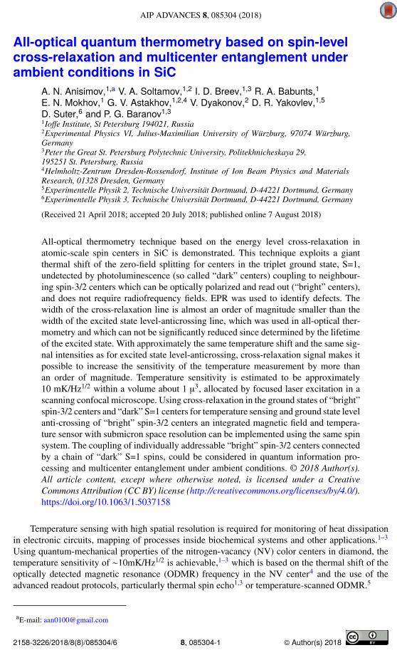
Figure 3 shows evolution of the PL as a function of the dc magnetic field B, recorded at differenttemperatures in 15R-SiC single crystal. A circles with a dot at 0.2, 0.9 and 2.48 mT indicate thecharacteristic magnetic fields of different “forbidden” GS LAC labeled as GS LAC1 for V3, V4 andV2 centers, respectively (following to Refs. 20 and 21 we will call the LAC between the two levelswith �MS = ±1 as “allowed” and with �MS = ±2 as “forbidden”). Vertical solid and dash lines reflectthe absence of temperature dependence for D parameters for the GS LAC; solid lines are drawn forGS LAC1 (B=D/�), dashed for “allowed” LACs denoted by LAC2 (B=2D/�).
The oblique dashed lines reflect the changes in the position of the ES LAC points (squares, widelines) and “bright-dark” CR (circles, narrow lines). The upper insert shows a shift in the CR lineswith a temperature change from 161 K to 257 K. The lower insert shows a shift of one of the CR lineswith a temperature change from 35 C to 42 C - possible temperature changes for the living system,a noise track is also shown.
The dotted line shows the the experimental points (crosses) from EPR measurements and sim-ulated temperature dependence of the D(T)/2 for “dark” S=1 centers. In the range 180-300 K, theCR magnetic field BCR versus temperature is reasonable to approximate by a linear function BCR=B0 - k⇤T; �BCR = - k⇤�T. �BCR can be then converted to temperature using �T = -�BCR/k. For themost intense peaks CR1: B0 = 21.8 mT; k = 0.017 mT/K; and CR2: B0 = 23.8 mT; k = 0.018 mT/K.
The temperature field will be measured at different points when the SiC crystal plate is scanned ina microscope. In this case, the object under investigation, for example, in the form of a film, is placeddirectly on a plate of active material in the form of silicon carbide for thermal contact, the thermalconductivity of silicon carbide is very high and it is possible to study various thermal processes inthe object of research (microelectronics chips, biological systems, where reactions take place withthe release of heat, etc.). Additional advantage over the diamond is the lack of an RF field.
The level anticrossing in the ground state does not depend on temperature, this is an additionaladvantage, since one effects can be used to determine the magnetic field (GS LAC), and others –(CRs) to determine the temperature. In this case, the same spin system is used, the desired object isselected only by applying a bias in the form of a constant magnetic field.
The technique for measuring temperature can be expanded by using SiC nanocrystals with thespin centers. The advantage of using vacancy-related spin centers in SiC in comparison with NVcenters diamond is the orientation of all spin centers along one axis, so instead of using singlecenters, it is convenient to use ensembles of such centers, which significantly increases the sensitivityof measurements. For example, a SiC nanocrystal with the spin centers can be placed on a probe ofan atomic force microscope or a near field microscope that directly contact the object under study.Such measurements are carried out by us and will be published later.”
The noise limit of measurements with one scan without accumulation and the measurementtime of about 0.1 sec is 3 µT (in the slope of the derivative). The seven degrees of the thermometer
085304-5 Anisimov et al. AIP Advances 8, 085304 (2018)
FIG. 3. Lock-in detection of the PL variation �PL as a function of the dc magnetic field B, recorded at different temperaturesin 15R-SiC single crystal. �PL is caused by the application of an additional weak oscillating magnetic field. RF is not applied.A circle with a dot indicates the characteristic magnetic fields of different “forbidden” LACs denoted by LAC1 (B=D) for theground state of the spin-3/2 center. Vertical solid and dashed lines reflect the absence of a change in the parameters of the finestructure (D) for the ground state of the spin centers with a change in temperature; solid lines are drawn for LAC1, dashed for“allowed” LACs denoted by LAC2 (B=2D). The oblique dashed lines reflect the changes in the position of the LAC pointsfor the excited state of the spin-3/2 centers (squares, wide lines) and cross-relaxation (circles, narrow lines). The upper insertshows a shift in the “bright-dark” cross-relaxation lines with a temperature change from 161 K to 257 K. For greater clarity,in the upper inset, the temperature increases in the opposite direction as compared to the main part of the figure. The lowerinsert shows a shift of one of the cross-relaxation lines with a temperature change from 35 C to 42 C - possible temperaturechanges for the living system. A noise track is shown. The dotted line shows the simulated temperature dependence of the finestructure splitting (as D/2) for “dark” spin-1 centers, the crosses denote the experimental points from EPR measurements.
(42 C-35 C) corresponds to a shift of⇠180 mkT (Fig. 3, bottom inset), that is 180 mkT/7 K = 25 mkT/K.It can be estimated that the sensitivity is approximately 100 mkK/Hz1/2. At lower temperatures, wehave sensitivity about five times higher, since the signal intensity has increased approximately 5times (Fig. 3, upper inset), that is, less than 20 mK/Hz1/2. When selecting more sensitive detectorsand optimizing the optical circuit, it is possible to achieve less then 10 mK/Hz1/2 in the volum of 1 µ3.

085304-6 Anisimov et al. AIP Advances 8, 085304 (2018)
For the concentration of spin centers of about 1016 -1017 cm-3, which was used in our experiments,in a volume of ⇠1 µ3 there are approximately 104-105 centers.
This work was supported by the by the RFBR under Grant No. 16-02-00877-a; by the RussianAcademy of Sciences; and the DFG in the frame of ICRC TRR 160. V.A.S. acknowledges supportthrough a sponsorship provided by the Alexander von Humboldt (AvH) foundation fellowship.
1 P. Neumann, I. Jakobi, F. Dolde, C. Burk, R. Reuter, G. Waldherr, J. Honert, T. Wolf, A. Brunner, J. H. Shim, D. Suter,H. Sumiya, J. Isoya, and J. Wrachtrup, Nano Letters 13, 2738 (2013).
2 G. Kucsko, P. C. Maurer, N. Y. Yao, M. Kubo, H. J. Noh, P. K. Lo, H. Park, and M. D. Lukin, Nature 500, 54 (2013).3 D. M. Toyli, C. F. de las Casas, D. J. Christle, V. V. Dobrovitski, and D. D. Awschalom, Proc. Natl. Acad. Sci. 110, 8417
(2013).4 V. M. Acosta, E. Bauch, M. P. Ledbetter, A. Waxman, L.-S. Bouchard, and D. Budker, Phys. Rev. Lett. 104, 070801 (2010).5 R. A. Babunts, A. A. Soltamova, D. O. Tolmachev, V. A. Soltamov, A. S. Gurin, A. N. Anisimov, V. L. Preobrazhenskii,
and P. G. Baranov, JETP Letters 95, 429 (2012).6 P. G. Baranov, I. V. Il’in, E. N. Mokhov, M. V. Muzafarova, S. B. Orlinskii, and J. Schmidt, JETP Lett. 82, 441 (2005).7 P. G. Baranov, A. P. Bundakova, I. V. Borovykh, S. B. Orlinskii, R. Zondervan, and J. Schmidt, JETP Lett. 86, 202 (2007).8 J. R. Weber, W. F. Koehl, J. B. Varley, A. Janotti, B. B. Buckley, C. G. Van de Walle, and D. D. Awschalom, Proc. Natl.
Acad. Sci. 107, 8513 (2010).9 D. DiVincenzo, Nat. Mater. 9, 468 (2010).
10 P. G. Baranov, A. P. Bundakova, A. A. Soltamova, S. B. Orlinskii, I. V. Borovykh, R. Zondervan, R. Verberk, and J. Schmidt,Phys. Rev. B 83, 125203 (2011).
11 D. Riedel, F. Fuchs, H. Kraus, S. Vath, A. Sperlich, V. Dyakonov, A. Soltamova, P. Baranov, V. Ilyin, and G. V. Astakhov,Phys. Rev. Lett. 109, 226402 (2012).
12 H. Kraus, V. A. Soltamov, F. Fuchs, D. Simin, A. Sperlich, P. G. Baranov, G. V. Astakhov, and V. Dyakonov, ScientificReports 4, 5303 (2014).
13 S. G. Carter, O. O. Soykal, P. Dev, S. E. Economou, and E. R. Glaser, Physical Review B 92, 161202 (2015).14 D. Simin, V. A. Soltamov, A. V. Poshakinskiy, A. N. Anisimov, R. A. Babunts, D. O. Tolmachev, E. N. Mokhov, M. Trupke,
S. A. Tarasenko, A. Sperlich, P. G. Baranov, V. Dyakonov, and G. V. Astakhov, Phys. Rev. X 6, 031014 (2016).15 M. Widmann, S.-Y. Lee, T. Rendler, N. T. Son, H. Fedder, S. Paik, L.-P. Yang, N. Zhao, S. Yang, I. Booker, A. Denisenko,
M. Jamali, S. Ali Momenzadeh, I. Gerhardt, T. Ohshima, A. Gali, E. Janzen, and J. Wrachtrup, Nature Materials 14, 164(2015).
16 D. J. Christle, A. L. Falk, P. Andrich, P. V. Klimov, J. u. Hassan, N. T. Son, E. Janzen, T. Ohshima, and D. D. Awschalom,Nature Materials 14, 160 (2015).
17 A. N. Anisimov, D. Simin, V. A. Soltamov, S. P. Lebedev, P. G. Baranov, G. V. Astakhov, and V. Dyakonov, ScientificReports 6, 33301 (2016).
18 V. A. Soltamov, B. V. Yavkin, D. O. Tolmachev, R. A. Babunts, A. G. Badalyan, V. Yu. Davydov, E. N. Mokhov,I. I. Proskuryakov, S. B. Orlinskii, and P. G. Baranov, Phys. Rev. Lett. 115, 247602 (2015).
19 G. V. Astakhov, D. Simin, V. Dyakonov, B. V. Yavkin, S. B. Orlinskii, I. I. Proskuryakov, A. N. Anisimov, V. A. Soltamov,and P. G. Baranov, Appl. Magn. Reson. 47, 793 (2016).
20 A. N. Anisimov, V. A. Soltamov, E. N. Mokhov, P. G. Baranov, G. V. Astakhov, and V. Dyakonov, Appl. Magn. Reson. 49,85 (2018).
21 P. G. Baranov, H.-J. von Bardeleben, F. Jelezko, and J. Wrachtrup, Magnetic Resonance of Semiconductors and TheirNanostructures: Basic and Advanced Applications: Springer Series in Materials Science Volume 253 (2017).
22 H. J. von Bardeleben, J. L. Cantin, E. Rauls, and U. Gerstmann, Phys. Rev. B 92, 064104 (2015).23 R. I. Epstein, F. M. Mendoza, Y. K. Kato, and D. D. Awschalom, Nature Physics 1, 94 (2005).24 N. M. Pavlov, M. I. Iglitsyn, M. G. Kosaganova, and V. N. Solomatin, Sov. Phys. Semicond. 9, 845 (1975).25 N. T. Son, P. Carlsson, J. ul Hassan, E. Janzen, T. Umeda, J. Isoya, A. Gali, M. Bockstedte, N. Morishita, T. Ohshima, and
H. Itoh, Phys. Rev. Lett. 96, 055501 (2006).

All-optical quantum thermometry based on spin-level cross-relaxation andmulticenter entanglement under ambient conditions in SiCA. N. Anisimov, V. A. Soltamov, I. D. Breev, R. A. Babunts, E. N. Mokhov, G. V. Astakhov, V. Dyakonov, D. R.Yakovlev, D. Suter, and P. G. Baranov
Citation: AIP Advances 8, 085304 (2018); doi: 10.1063/1.5037158View online: https://doi.org/10.1063/1.5037158View Table of Contents: http://aip.scitation.org/toc/adv/8/8Published by the American Institute of Physics