Embed Size (px)
Citation preview

Amphiphilic semiconducting copolymer as
compatibility layer for printing polyelectrolyte-
gated OFETs
Hiam Sinno, Ha Tran Nguyen, Anders Hägerström, Mats Fahlman, Linda Lindell,
Olivier Coulembier, Philippe Dubois, Xavier Crispin, Isak Engquist and Magnus Berggren
Linköping University Post Print
N.B.: When citing this work, cite the original article.
Original Publication:
Hiam Sinno, Ha Tran Nguyen, Anders Hägerström, Mats Fahlman, Linda Lindell, Olivier
Coulembier, Philippe Dubois, Xavier Crispin, Isak Engquist and Magnus Berggren,
Amphiphilic semiconducting copolymer as compatibility layer for printing polyelectrolyte-
gated OFETs, 2013, Organic electronics, (14), 3, 790-796.
http://dx.doi.org/10.1016/j.orgel.2012.12.031
Copyright: Elsevier
http://www.elsevier.com/
Postprint available at: Linköping University Electronic Press
http://urn.kb.se/resolve?urn=urn:nbn:se:liu:diva-88980

EGOFET: Polyelectrolyte-gated organic field effect transistor. 1
BC: Block copolymer.
Amphiphilic semiconducting copolymer as compatibility layer for printing
polyelectrolyte-gated OFETs
Hiam Sinnoa, Ha Tran Nguyen
b, Anders Hägerström
a, Mats Fahlman
c, Linda Lindell
c, Olivier
Coulembierb, Philippe Dubois
b, Xavier Crispin
a, Isak Engquist
a,*, Magnus Berggren
a
a Department of Science and Technology, Organic Electronics, Linköping University, SE-601 74 Norrköping
(Sweden) b Laboratory of Polymeric and Composite Materials, Center of Innovation and Research in Materials and
Polymers (CIRMAP), University of Mons-UMONS, Place du Parc 23, 7000 Mons (Belgium) c Department of Physics, Chemistry and Biology, Linköping University, SE-581 83 Linköping (Sweden)
* Corresponding author. Tel.: +46 11 363401; fax: +46 11 363270.
E-mail address: [email protected] (I. Engquist).
Abstract
We report a method for inkjet-printing an organic semiconductor layer on top of the
electrolyte insulator layer in polyelectrolyte-gated OFETs by using a surface modification
treatment to overcome the underlying wettability problem at this interface. The method
includes depositing an amphiphilic diblock copolymer (P3HT-b-PDMAEMA). This material
is designed to have one set of blocks that mimics the hydrophobic properties of the
semiconductor (poly(3-hexylthiophene) or P3HT), while the other set of blocks include polar
components that improve adhesion to the polyelectrolyte insulator. Contact angle
measurements, atomic force microscopy, and x-ray photoelectron spectroscopy confirm
formation of the desired surface modification film. Successful inkjet printing of a smooth
semiconductor layer allows us to manufacture complete transistor structures that exhibit low-
voltage operation in the range of 1 V.
Keywords: Block Copolymers, Inkjet Printing, Organic Field-Effect Transistors, Organic
Electronics, Printed Electronics
1. Introduction
Printed organic electronics combines the flexibility of organic materials with the low cost,
robustness, and high throughput of printing technologies.[1, 2] In a majority of printed circuits,
2
organic field effect transistors (OFETs) are essential components, and substantial research
efforts have been dedicated to achieve transistors that combine printability with low-voltage
operation. To this end, several groups have previously demonstrated electrolyte-gated OFETs
(EGOFETs) fabricated using spin-coating and thermal evaporation techniques. The EGOFETs
differ from conventional OFETs in the sense that an electrolyte is included as the gate insulator
material instead of a dielectric layer.[3-5] Gating via an electrolyte enables the formation of
electric double-layers (EDLs) at the gate/electrolyte and electrolyte/semiconductor interfaces
upon gate biasing, induced by ion migration within the polyelectrolyte. The EDLs provide
transistor configurations with high interfacial capacitances that make device operation at low
voltages possible.[3-5] These qualities make EGOFETs suitable to manufacture using printing
techniques since ultra-high resolution is typically difficult to achieve. However, several
challenges have to be overcome when attempting to achieve a fully printed EGOFET. One of
the main problems faced relates to adhesion properties at the semiconductor/electrolyte
interface and is attributed to incompatible wetting characteristics. The common p-type
semiconducting materials are typically hydrophobic, whereas the common polyelectrolyte
materials are hydrophilic, which makes it difficult to print these two layers as a stack on top of
each other. Thus, one of the main challenges in the production of EGOFETs is to find a
suitable combination of materials and solvents having matched wettability characteristics but
that do not dissolve each other.
Previous attempts towards all-printed EGOFETs include aerosol-jet-printed thin-film
transistors gated ion-gels.[6] Such devices include a gelled electrolyte, based on an ionic liquid
and a gelating block copolymer, as the gate insulator. This gel electrolyte is hydrophobic
which makes deposition on top of the hydrophobic poly(3-hexylthiophene) P3HT
semiconductor easy. However, one draw-back is that the anions from the gel can penetrate into
the polymer bulk which leads to unwanted electrochemical reactions in the semiconductor.[7]

3
Another approach to achieve working electrolyte-gated transistors is the all printed
hygroscopic insulator field effect transistor (HIFET)[8] where reverse gravure coating was
used to apply the semiconductor and insulator.[9] This transistor also relies on
oxidation/reduction of the semiconductor by ions from the electrolyte. Printed electrolytes
have also been used in electrochemical transistors and can be fabricated both by inkjet[10] and
screen printing[11]. The aim of this work is to demonstrate a method to print the organic
semiconductor on top of the polyelectrolyte to enable all-printed processing of EGOFETs.
In this work, we are addressing the most crucial fabrication step to manufacture EGOFETs,
which is the semiconductor/electrolyte interface, where wettability incompatibilities have to be
overcome and where a smooth and homogeneous interface is crucial for the performance of the
transistor. We have investigated a surface modification treatment of the electrolyte film by the
aid of a diblock copolymer (BC) to render the film relatively more hydrophobic, thereby
enhancing the printability of the hydrophobic semiconductor layer on top. A BC derivative has
been synthesized composed of two blocks that chemically mimic the properties of the
semiconductor and the electrolyte, respectively. With this material we aim to promote the
printability of the semiconductor without interfering electrically with the functionality of the
transistor, since the hydrophobic semiconducting block in the copolymer is expected to be part
of the semiconducting channel of the transistor. In contrast with typical insulating amphiphilic
interfacial agents, the presence of a semiconducting block ensures close distance between the
electronic charge carriers migrating along the semiconducting channel and the ionic charge
carriers that form the EDLC at the semiconductor/electrolyte interface. A bottom-gate structure
was implemented here because preliminary experiments show that it is not possible to do a top
gate configuration using the BC-treatment. We believe that the amine group in the BC is
attracted to the negatively charged polyelectrolyte which leads to the formation of a layer of
BC molecules on the polyelectrolyte surface with the polythiophene segment part facing
4
outward towards the semiconducting layer. This driving force for BC layer formation is not
present in the top-gate structure where the BC would be deposited on the semiconductor. Thus,
our BC-treatment is suitable for use only when the semiconducting layer is printed on top of
the electrolyte layer. Inkjet printing was selected as the deposition method because of its
flexibility and short lead-time for small sample series, and because wettability incompatibility
is a well-known issue for this printing technique.[12-15] Also, with inkjet printing we can
deliver a wide range of functional materials while minimizing material waste.
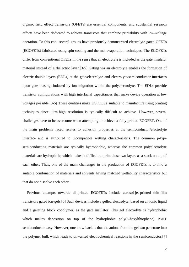
The block copolymer P3HT-b-PDMAEMA (Fig. 1) consists of a poly(3-hexylthiophene)
block (molar mass, Mn ~ 7,000 g mol-1
) covalently linked to a poly(N,N-dimethylaminoethyl
methacrylate) segment (Mn ~ 16,500 g mol-1
). This combination of conjugated and non-
conjugated segments results in a material that can phase-segregate into nanostructures due to
the immiscibility of the covalently connected blocks. A detailed description of the synthesis of
a polymer of this class is given in another paper.[16]
Figure 1. Chemical structure of the diblock copolymer P3HT-b-PDMAEMA.

5
2. Experimental
2.1. Synthesis of poly(3-hexylthiophene)-block-poly(N,N-dimethylaminoethyl methacrylate)
(P3HT-b-PDMAEMA):
The polymerization was performed in anhydrous THF by using P3HT-Br (or P3HT-MI),
CuBr, and HMTETA as macroinitiator, catalyst, and ligand, respectively. The initial molar
ratio was [M]0:[P3HT-MI]0:[CuBr]0:[HMTETA]0 = 100:1:1:2. A dry flask was charged with
CuBr (4.1 mg, 0.028 mmol), HMTETA (15.7 μl, 0.057 mmol), THF (1 ml), and a magnetic
stirrer. The flask was fitted with a rubber septum and degassed with three successive vacuum
nitrogen cycles. A second flask was charged with the P3HT-MI (200 mg, Mn = 7000 g mol-1
,
0.02857 mmol), DMAEMA monomer (0.5 ml, 450 mg, 2.857 mmol), and THF (2 ml). The
flask was fitted with a rubber septum and degassed under nitrogen flow for a few minutes. The
mixture was then transferred into the first flask and the polymerization was carried out under
stirring at 60 °C for 16 hours. The reaction was stopped by cooling down the reaction medium
in liquid nitrogen. Then, THF was added to dilute the solution. Copper catalyst was removed
by filtration of the THF solution through an alumina oxide column. The diblock copolymers
were recovered by precipitation from cold heptane, filtration and drying up to constant weight.
1H NMR (300 MHz, CDCl3); δ (ppm): 6.96 (s, 1H), 5.29 (s, 2H), 4.06 (s, 2H), 2.78 (t, 2H),
2.57 (s, 2H), 2.28 (s, 6H), 1.90 (s, 2H), 1.69 (sex, 2H), 1.49 (q, 6H), 1.04 (s, 9H), 0.89 (t, 3H).
MnGPC ~ 19300 g mol-1
. Ð, 1.7. MnNMR ~ 23,500 g mol-1
.
2.2. Device fabrication:
The p-type EGOFET was manufactured by thermally evaporating (50 nm thick) gold (Au)
on top of (5 nm thick) chromium (Cr) (bottom gate electrode) through a shadow mask on a
Si/SiO2 wafer. A (100 nm thick) polyelectrolyte film consisting of a mixture of 1:14 vol:vol
poly(styrene sulfonic acid) (PSSH, Sigma-Aldrich with a molecular weight of about 75 000
and a concentration of 18 wt. % in de-ionized water) to de-ionized water with 0.3% zonyl as a

6
surfactant was spincoated on top of the gate electrode and annealed under vacuum at 110 °C
for 90 s. Then, a PSSH film treatment was performed by dipping the sample in a solution
consisting of (0.01 mg ml-1
P3HT-b-PDMAEMA in toluene) for 1 minute. The samples were
ultrasonicated in toluene for 5 minutes to remove excess layers of the BC and to break any BC
micelles in order to achieve good contact with the PSSH surface. The organic semiconductor
solution consisting of 4 mg ml-1
regioregular poly(3-hexylthiophene) (rr-P3HT, Sigma-Aldrich
with a regioregularity greater than 95% and a molecular weight of 15 000 - 45 000) in 68%
ortho-dichlorobenzene (oDCB) and 32% mesitylene was printed using the Dimatix material
printer DMP-2800 forming a relatively continuous film (40 nm thick). The semiconductor
solvent formulation and the printer platen temperature control the wetting and drying behavior
of the printed semiconductor film on the PSSH electrolyte layer. A pure oDCB formulation
results in poor spreading and wettability of the printed film because of its high surface tension
and high boiling point; therefore, mesitylene was added to the solvent formulation since it has
a lower boiling point and lower surface tension. The ratio of solvents was chosen according to
a previous reported study that shows this formulation to provide an optimum wettability of the
printed film on top of PEDOT:PSS.[17] Cartridges with a 10 pl drop volume were used, the
drop spacing was set to 40 μm, a single nozzle was used for jetting the P3HT solution with a
maximum jetting frequency of 10 kHz, and the printer platen temperature was set to 30 °C.
The rr-P3HT film was annealed under nitrogen at 120 °C for 10 minutes. Finally, (100 nm
thick) Au was thermally evaporated through a shadow mask forming the source and drain top
contacts. The channel length and width of the transistor were 10 µm and 700 µm respectively.
The structure of our device is shown in Fig. 2. For comparison reasons, a sample with a
spincoated PSSH film was treated with a common surfactant (dodecyltrimethylammonium
chloride in diethylcarbonate) by dipping it in this solution for 1 minute and then rinsing it in
toluene where the sample was ultrasonicated for 5 minutes to get rid of excess layers of the

7
surfactant. Then, a rr-P3HT layer was inkjet-printed on top of the treated PSSH layer using the
same parameters indicated above.
Figure 2. EGOFET design structure. The critical semiconductor/electrolyte is marked with a
dotted line. The external circuit used for transistor measurements is also indicated.
2.3. Device characterization:
Contact angle measurements were recorded using a goniometer (CAM 200, KSV). The
AFM images were obtained using a Veeco Dimension 3100 atomic force microscopy (AFM).
X-ray photoelectron spectroscopy (XPS) measurements were performed using a Scienta ESCA
200 instrument. The transistor characteristics reported here were measured with a Keithley
4200-SCS parameter analyzer. All electrical measurements were made in ambient air (relative
humidity ca. 40%) at room temperature.
3. Results and discussion
The block copolymer treatment was performed by dipping the PSSH-coated sample in a
solution of P3HT-b-PDMAEMA dissolved in toluene. It is important to use a non-polar
solvent such as toluene in order to avoid dissolving the underlying PSSH layer. To some
extent, this will result in the formation of micelles in the solution, as evidenced by the
previously reported differences in the absorption spectra of the BC in polar and non-polar
solvents, respectively.[16] We expect these micelles to break in contact with the polar PSSH
surface and contribute to the formation of a BC film; however, it will be seen below that a few

8
defects remain which we believe can be removed by further optimization of the solvent
formulation.
Contact angle measurements of hexadecane and DI-water on the spin-coated PSSH film
prior to and after the BC-treatment have been recorded using a goniometer, with results shown
in Table 1. Various BC-treatment times were investigated to find the shortest treatment that
would yield the sought-after wettability improvement. The contact angles change considerably
after the BC-treatment indicating a less hydrophilic surface, which should promote printability
of the rr-P3HT solution on top of the electrolyte. We can see that longer treatment times results
in lower hexadecane contact angles, but that already 1 minute treatment causes a significant
drop compared to the untreated surface. We have proceeded with the short 1 minute BC-
treatment time since the change in the contact angle was sufficient to achieve printability and
since the thinnest possible BC layer is desirable in order to avoid degradation of transistor
performance. The contact angle measurements were conducted on 10 different samples for
each treatment, with mean values and standard deviation shown in Table 1. The low standard
deviation values indicate that the treatment is repeatable.
The surface tension or surface free energy (SFE) of both samples was calculated using the
Owens–Wendt theoretical model.[18] The model estimates the long-range dispersion
(Lifshitz–Van derWaals, γd) and the short-range polar (hydrogen bonding, γ
p) components of
SFE according to the following equation:
(1 + cosθ) γl = 2 (γsd)1/2 (γl
d)1/2
+ 2 (γsp)1/2
(γlp)1/2
(1)
where γs and γl are the SFE of the surface and the liquid respectively, and θ is the contact
angle. The overall surface tension γ is a combination of dispersive γd and polar γ
p components.
Substituting both contact angle and surface tension values of DI-water and hexadecane (at 21
°C, DI water: γ = 72.8 mN m-1
, γd = 21.8 mN m
-1, γ
p = 51 mN m
-1; Hexadecane: γ = 27.47 mN

9
m-1
, γd = 27.47 mN m
-1, γ
p = 0 mN m
-1)[19] in Equation 1, the samples surface tension were
calculated and are shown in Table 1.
Table 1. Contact angle data for pristine rr-P3HT and PSSH, and for BC-treated surfaces, and
calculated surface tension (γ), dispersive (γd) and polar (γ
p) components of the surface tension
of all samples at 20 °C. The contact angle measurements were conducted on 10 samples for
each treatment and the mean values and standard deviations are given. Contact angles [°]
Samples DI water Hexadecane
Pristine rr-P3HT 101.63 ± 0.26 32.78 ± 0.42
Pristine PSSH 18.74 ± 0.35 50.54 ± 0.86
BC-treated PSSH
1 minute 44.49 ± 0.15 39.01 ± 0.14
5 minutes 46.66 ± 0.11 38.66 ± 0.18
30 minutes 49.60 ± 0.14 35.65 ± 0.15
1 hour 52.42 ± 0.18 31.59 ± 0.19
10 hours 59.4 ± 0.30 26. 14 ± 0.46
Surface tension (γ, mN m-1) at 20 °C
Samples γ γd γ
p
Pristine rr-P3HT 24.1 ± 0.05 23.26 ± 0.10 0.83 ± 0.05
Pristine PSSH 69.08 ± 0.16 18.36 ± 0.26 50.71 ± 0.42
BC-treated PSSH
1 minute 54.04 ± 0.10 21.69 ± 0.03 32.35 ± 0.13
5 minutes 52.51 ± 0.06 21.78 ± 0.04 30.73 ± 0.11
30 minutes 50.59 ± 0.09 22.56 ± 0.03 28.03 ± 0.12
1 hour 48.87 ± 0.12 23.55 ± 0.04 25.32 ± 0.16
10 hours 44.44 ± 0.17 24.73 ± 0.09 19.71 ± 0.26
It can be seen from both contact angle and surface tension data presented in Table 1 that the
electrolyte layer is rendered more hydrophobic after the BC-treatment thus enhancing the
printability of the rr-P3HT semiconductor layer on top. We conclude that although a dilute BC
solution was used, and the treatment time was short (1 minute), the desired surface
modification has taken place. Obviously, a fully P3HT-like surface has not been achieved, but
the aim here is to obtain a surface where rr-P3HT can be inkjet-printed using an interlayer that
is as thin and smooth as possible.
10
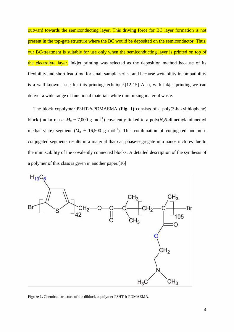
Atomic force microscopy (AFM) measurements of the PSSH electrolyte surface were
performed before and after the BC-treatment. Results are shown in Fig. 3. We observe that the
roughness of the BC-treated PSSH surface is larger and that the film exhibits more texture than
the untreated surface. RMS roughness values are 0.14 nm for the untreated PSSH surface and
0.7 nm for the BC-treated PSSH surface. These results indicate that the BC-treatment results in
the formation of a layer of the diblock copolymer on top of the PSSH surface with a different
surface morphology still smooth to provide a good template for the following process steps. In
Fig. 3b, we note a few elevated areas spread over the surface that are about 3 to 4 nm high and
may consist of unbroken micelles. However, given their small height and area, they should be
of little significance for the following printing of P3HT.
Figure 3. AFM height images of the (a) untreated and (b) BC treated PSSH electrolyte
surfaces.
The BC-treatment results were also investigated by XPS. Measurements were performed on
an untreated PSSH film coated on a Si substrate and also on a BC-treated PSSH film according
to the standard process described in the experimental section. Normal emission (flat) and 67°
glancing angle emission (tilted) measurement geometries were used for both samples. Of

11
special interest are the S(2p) peaks, shown in Fig. 4 for the untreated and the BC-treated
samples. The untreated PSSH surface (Fig. 4a) gives rise to a high binding energy double peak
at (168 - 172 eV), originating from the sulfonate group due to the presence of three
electronegative oxygen atoms in the surrounding.[20] In the S(2p) narrow scan of the BC-
treated PSSH surface (Fig. 4b), the high binding energy peak originates from the PSSH layer
while the low binding energy peak (164 - 167 eV) originates from the thiophene part of the BC
film. The existence of the thiophene peak proves that the BC-treatment was successful. The
intensity of the thiophene peak is quite low which indicates that the copolymer layer is very
thin. The increase in the thiophene/sulfonate signal ratio when the sample is tilted (‘‘flat‘‘
versus ‘‘tilted‘‘ in the 164 - 167 eV region of Fig. 4b) indicates that the copolymer film is at
the surface of the PSSH layer, which is in agreement with the contact angle and surface tension
data.
Figure 4. (a) XPS narrow-scan of S(2p) peak for the untreated PSSH surface (flat and tilted
emission), (b) XPS narrow-scan of S(2p) peak for BC treated PSSH surface (flat and tilted
emission).
In Fig. 5, the difference between an inkjet printed rr-P3HT layer on top of untreated and 1-
minute BC-treated PSSH films is shown (Fig. 5 a and b). The printed P3HT film on top the

12
untreated PSSH layer results in the formation of de-wetted lines corresponding to the passage
of the inkjet printer head. It is clear that the resulting printed rr-P3HT film on top of the
untreated PSSH film is inhomogeneous and has many dewetting spots while the printed rr-
P3HT film on top of the BC-treated PSSH film completely wets the electrolyte film and is
essentially homogeneous. This is direct proof that the BC-treatment provides the desired global
surface modification effect that enables printing fabrication of the polymer semiconductor on
top of the polyelectrolyte insulator. For the purpose of comparison, a PSSH film was also
treated with a common surfactant (dodecyltrimethylammonium chloride in diethylcarbonate),
but attempts to inkjet-print the rr-P3HT layer on top resulted in an inhomogeneous film with a
high density of dewetting spots, similar to the results for the untreated PSSH (Fig. 5c).
Additionally, an image of the 1-minute BC-treated PSSH electrolyte film is shown in Fig. 5d.
We can see that the BC-treatment results in the formation of a few “white dots” spread over the
BC film, possibly consisting of aggregates of unbroken micelles as mentioned above. After
printing the semiconductor layer, these white dots appear as defects in the form of black spots
as seen in Fig. 5b. We expect that further optimization of the BC-treatment will remove the
micelles and thereby also these defects. Summarizing our measurements, the diblock
copolymer treatment of the PSSH electrolyte layer has been shown to enhance the printability
of the rr-P3HT semiconducting layer to a point where a continuous film is obtained, which
holds promise for the fabrication of a working transistor.

13
Figure 5. Optical microscopy images of (a) an inkjet-printed rr-P3HT film on top of untreated PSSH electrolyte
film, (b) inkjet-printed rr-P3HT film on top of 1-minute BC-treated PSSH electrolyte film, (c) inkjet-printed rr-
P3HT film on top of dodecyltrimethylammonium-chloride-in-diethylcarbonate-treated PSSH electrolyte film, (d)
1 minute BC-treated PSSH electrolyte film. The formation of the lines in the untreated and surfactant treated
images (a and c) corresponds to the passage of the printer head. The gold-colored stripe at the bottom of images (a
and b) is the bottom Au gate.
As a final step, full EGOFETs were fabricated for electrical characterization. This was
obviously only possible on BC-treated samples. The resulting EGOFET transistors (10
samples) were electrically characterized. Transfer and output curves of one of the fabricated
transistors are shown in Fig. 6a and Fig. 6b, respectively. The obtained on/off current ratio
Ion/Ioff = 40 ± 6. This is lower, but in the same order of magnitude, as compared to an identical
EGOFET manufactured using spin-coating without BC-treatment (Ion/Ioff ≈ 100). The leakage
current (gate current) is typically less than one order of magnitude lower than ID at a given
voltage. The threshold voltage is found to be -0.63 ± 0.05 V which is higher than the typical
value observed in identical transistors manufactured with spin-coating (VT = -0.45 V). The

14
field effect mobility at saturation is estimated to be 0.15 ± 0.004 cm2 V
-1 s
-1 (calculated for Ci =
3 μF cm-2
, at VD = -1 V and VG = -1.5 V). The EGOFET shows a minor hysteresis behavior
between the upward and downward scans for the transfer curve which we attribute to the fact
that the accumulation of charges in the channel takes a few seconds (sweep rate of the upward
scan is around 10 s), and thus at the end of the downward scan of the transfer curve, the density
of accumulated charges is higher which leads to a higher drain current. Overall, the transistor
performance is not impressive and the on/off ratio is lower compared to conventional
EGOFETs that are fabricated using spin-coating, vacuum evaporation, and photolithography
patterning techniques. We believe this to be partly due to the use of the bottom-gate structure
(for reasons stated above) which exposes the semiconductor to the ambient atmosphere. Also,
the presence of the BC layer adds a thin interface to the critical zone where field effect takes
place. However, it is clear that a working transistor can be built and we are confident that
improved processing and optimized BC-treatment can improve the performance. Thus, the
present measurements demonstrate the potential of the BC-treatment as a route towards low
cost all-printed circuit applications.
4. Conclusions
In conclusion, we have shown that by applying a surface modification treatment to the
hydrophilic electrolyte film using the P3HT-b-PDMAEMA diblock copolymer we can render
the film more hydrophobic. This enables inkjet-printing of the hydrophobic rr-P3HT
semiconductor layer on top of the electrolyte layer while minimizing the electrical influence on
the functionality of the transistor, since the composition of the BC matches the materials
surrounding it. This approach enables the production of low-voltage EGOFETs with inkjet-
printed rr-P3HT semiconductor layer providing a route towards all-inkjet printed electronics.

15
Figure 6. Current-voltage characteristics of a p-type EGOFET with inkjet-printed rr-P3HT layer having 10 μm
channel length and 700 μm channel width. (a) Transfer curve with an inset showing the threshold voltage
extraction from the linear fit to the square root of the drain current, (b) Output curves measured at the following
VG values 0, -0.21 V, -0.42 V, -0.64 V, -0.85 V, -1.07 V, -1.28 V, -1.5 V.
Acknowledgements
This work has been supported by Acreo, PEA-VINNOVA and PEA-PPP-TVV, OPEN-SSF,
Önnesjö, KAW, the European Commission and Région Wallonne FEDER program (Materia-
Nova) and OPTI²MAT program of excellence, the Interuniversity Attraction Pole program of
the Belgian Federal Science Policy Office (PAI 6/27) and by FNRS-FRFC. O.C. is FNRS
Research Associate.
References
[1] H. Ma, H.-L. Yip, F. Huang, A.K.Y. Jen, Interface Engineering for Organic Electronics,
Adv. Funct. Mater., 20 (2010) 1371-1388.
[2] M. Berggren, D. Nilsson, N.D. Robinson, Organic materials for printed electronics, Nat.
Mater. , 6 (2007) 3-5.
[3] L. Herlogsson, X. Crispin, N.D. Robinson, M. Sandberg, O.J. Hagel, G. Gustafsson, M.
Berggren, Low-Voltage Polymer Field-Effect Transistors Gated via a Proton Conductor, Adv.
Mater., 19 (2007) 97-101.
[4] O. Larsson, E. Said, M. Berggren, X. Crispin, Insulator Polarization Mechanisms in
Polyelectrolyte-Gated Organic Field-Effect Transistors, Adv. Funct. Mater., 19 (2009) 3334-
3341.
[5] E. Said, X. Crispin, L. Herlogsson, S. Elhag, N.D. Robinson, M. Berggren, Polymer field-
effect transistor gated via a poly(styrenesulfonic acid) thin film, Appl. Phys. Lett., 89 (2006)
143507-143510.
[6] Y. Xia, W. Zhang, M. Ha, J.H. Cho, M.J. Renn, C.H. Kim, C.D. Frisbie, Printed Sub-2 V
Gel-Electrolyte-Gated Polymer Transistors and Circuits, Adv. Funct. Mater., 20 (2010) 587-
594.
[7] J.H. Cho, J. Lee, Y. Xia, B. Kim, Y. He, M.J. Renn, T.P. Lodge, D. Frisbie, Printable ion-
gel gate dielectrics for low-voltage polymer thin-film transistors on plastic, Nat. Mater., 7
(2008) 900-906.
[8] T.G. Bäcklund, H.G.O. Sandberg, R. Österbacka, H. Stubb, Current modulation of a
hygroscopic insulator organic field-effect transistor, Appl. Phys. Lett., 85 (2004) 3887-3889.

16
[9] D. Tobjö ِ rk, N.J. Kaihovirta, T. Mäkelä, F.S. Pettersson, R. Österbacka, All-printed low-
voltage organic transistors, Org. Electron., 9 (2008) 931-935.
[10] L. Basiricò, P. Cosseddu, A. Scidà , B. Fraboni, G.G. Malliaras, A. Bonfiglio, Electrical
characteristics of ink-jet printed, all-polymer electrochemical transistors, Org. Electron., 13
(2012) 244-248.
[11] T. Blaudeck, P.A. Ersman, M. Sandberg, S. Heinz, A. Laiho, J. Liu, I. Engquist, M.
Berggren, R.R. Baumann, Simplified Large-Area Manufacturing of Organic Electrochemical
Transistors Combining Printing and a Self-Aligning Laser Ablation Step, Adv. Funct. Mater.,
(2012).
[12] P. Calvert, Inkjet Printing for Materials and Devices, Chem. Mater., 13 (2001) 3299-
3305.
[13] J.Z. Wang, Z.H. Zheng, H.W. Li, W.T.S. Huck, H. Sirringhaus, Dewetting of conducting
polymer inkjet droplets on patterned surfaces, Nat. Mater., 3 (2004) 171-176.
[14] F. Varela, E. Armendariz, C. Wolluschek, Inkjet printed electronics: The wet on wet
approach, Chem. Eng. Process., 50 (2011) 589-591.
[15] M. Plötner, T. Wegener, S. Richter, S. Howitz, W.J. Fischer, Investigation of ink-jet
printing of poly-3-octylthiophene for organic field-effect transistors from different solutions,
Synth. Met., 147 (2004) 299-303.
[16] H. Nguyen, O. Coulembier, J. De Winter, P. Gerbaux, X. Crispin, P. Dubois, Novel
regioregular poly(3-hexylthiophene)-based polycationic block copolymers, Polym. Bull., 66
(2011) 51-64.
[17] C.N. Hoth, S.A. Choulis, P. Schilinsky, C.J. Brabec, High Photovoltaic Performance of
Inkjet Printed Polymer:Fullerene Blends, Adv. Mater., 19 (2007) 3973-3978.
[18] G. Lamour, A. Eftekhari-Bafrooei, E. Borguet, S. Souès, A. Hamraoui, Neuronal
adhesion and differentiation driven by nanoscale surface free-energy gradients, Biomaterials,
31 (2010) 3762-3771.
[19] D.Y. Kwok, D. Li, A.W. Neumann, Evaluation of the Lifshitz-van der Waals/Acid-Base
Approach To Determine Interfacial Tensions, Langmuir, 10 (1994) 1323-1328.
[20] X. Crispin, S. Marciniak, W. Osikowicz, G. Zotti, A.W.D. van der Gon, F. Louwet, M.
Fahlman, L. Groenendaal, F. De Schryver, W.R. Salaneck, Conductivity, morphology,
interfacial chemistry, and stability of poly(3,4-ethylene dioxythiophene)–poly(styrene
sulfonate): A photoelectron spectroscopy study, J. Polym. Sci., Part B: Polym. Phys. , 41
(2003) 2561-2583.