Embed Size (px)
Citation preview

Application ReportSNOA660A–May 2004–Revised Mat 2013
AN-103 LM340 Series Three Terminal Positive Regulators.....................................................................................................................................................
ABSTRACT
The LM340-XX are three terminal 1.0A positive voltage regulators, with preset output voltages of 5.0V or15V. The LM340 regulators are complete 3-terminal regulators requiring no external components fornormal operation. However, by adding a few parts, one may improve the transient response, provide for avariable output voltage, or increase the output current. Included on the chip are all of the functional blocksrequired of a high stability voltage regulator; these appear in Figure 1.
Contents1 Introduction .................................................................................................................. 32 Circuit Design ................................................................................................................ 3
2.1 Voltage Reference ................................................................................................. 32.2 Simplified LM340 ................................................................................................... 42.3 Complete Circuit of the LM340 ................................................................................... 52.4 Short Circuit Protection ............................................................................................ 52.5 Thermal Shut Down ................................................................................................ 62.6 Power Dissipation .................................................................................................. 6
3 Current Source .............................................................................................................. 74 High Current Regulator with Short Circuit Current Limit ............................................................... 85 5.0V, 5.0A Voltage Regulator for TTL .................................................................................. 106 Adjustable Output Voltage Regulator for Intermediate Output Voltages ........................................... 107 Variable Output Regulator ................................................................................................ 128 Variable Output Regulator 0.5V–29V ................................................................................... 139 Dual Power Supply ........................................................................................................ 1510 Tracking Dual Regulators ................................................................................................ 1511 High Input Voltage ......................................................................................................... 1712 High Voltage Regulator ................................................................................................... 1813 Electronic Shutdown ...................................................................................................... 1914 Variable High Voltage Regulator with Overvoltage Shutdown ...................................................... 2015 Bibliography ................................................................................................................ 20
List of Figures
1 Functional Block of the LM340 ............................................................................................ 3
2 Simplified Volt Reference .................................................................................................. 4
3 LM340 Simplified............................................................................................................ 5
4 Complete Circuit of the LM340............................................................................................ 6
5 Current Source .............................................................................................................. 7
6 15V 5.0A Regulator with Short Circuit Current Limit ................................................................... 8
7 Maximum Instantaneous Current vs Junction Temperature........................................................... 9
8 Continuous Short Circuit Current vs Input Voltage ..................................................................... 9
9 Load Regulation ........................................................................................................... 10
10 10V Regulator.............................................................................................................. 10
11 5.0V, 5.0A Regulator for TTL (with short circuit, thermal shutdown protection, and overload indicator) ...... 11
12 Variable Output Regulator................................................................................................ 12
All trademarks are the property of their respective owners.
1SNOA660A–May 2004–Revised Mat 2013 AN-103 LM340 Series Three Terminal Positive RegulatorsSubmit Documentation Feedback
Copyright © 2004–2013, Texas Instruments Incorporated
www.ti.com
13 Maximum Output Current................................................................................................. 13
14 Variable Output Voltage 0.5V−30V ..................................................................................... 14
15 Typical Load Regulation for a 0.5V−30V Regulator (ΔIOUT = 1.0A) ................................................. 15
16 Dual Power Supply ........................................................................................................ 16
17 Tracking Dual Supply ±5.0V − ±18V .................................................................................... 16
18 Tracking Dual Supply ±15V .............................................................................................. 17
19 High Input Voltage......................................................................................................... 18
20 High Input Voltage......................................................................................................... 18
21 High Voltage Regulator ................................................................................................... 18
22 Electronic Shutdown Circuit .............................................................................................. 19
23 Variable High Voltage Regulator with Shortcircuit and Overvoltage Protection................................... 20
2 AN-103 LM340 Series Three Terminal Positive Regulators SNOA660A–May 2004–Revised Mat 2013Submit Documentation Feedback
Copyright © 2004–2013, Texas Instruments Incorporated
www.ti.com Introduction
1 Introduction
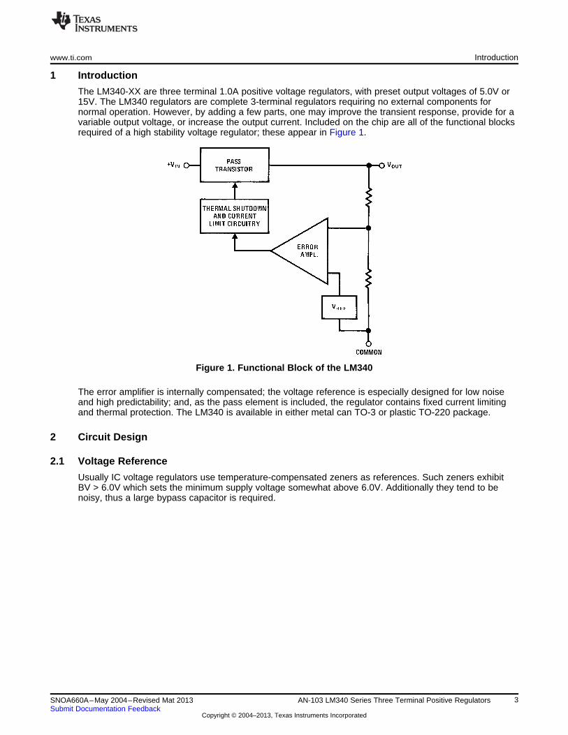
The LM340-XX are three terminal 1.0A positive voltage regulators, with preset output voltages of 5.0V or15V. The LM340 regulators are complete 3-terminal regulators requiring no external components fornormal operation. However, by adding a few parts, one may improve the transient response, provide for avariable output voltage, or increase the output current. Included on the chip are all of the functional blocksrequired of a high stability voltage regulator; these appear in Figure 1.
Figure 1. Functional Block of the LM340
The error amplifier is internally compensated; the voltage reference is especially designed for low noiseand high predictability; and, as the pass element is included, the regulator contains fixed current limitingand thermal protection. The LM340 is available in either metal can TO-3 or plastic TO-220 package.
2 Circuit Design
2.1 Voltage Reference
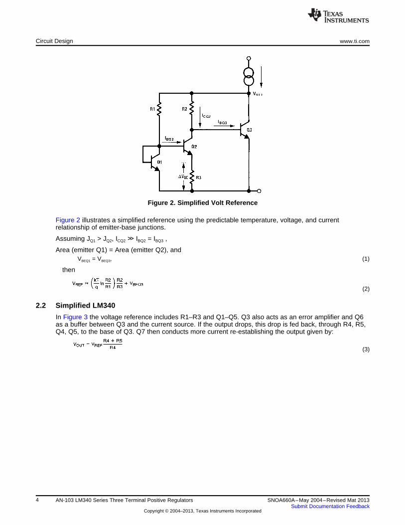
Usually IC voltage regulators use temperature-compensated zeners as references. Such zeners exhibitBV > 6.0V which sets the minimum supply voltage somewhat above 6.0V. Additionally they tend to benoisy, thus a large bypass capacitor is required.
3SNOA660A–May 2004–Revised Mat 2013 AN-103 LM340 Series Three Terminal Positive RegulatorsSubmit Documentation Feedback
Copyright © 2004–2013, Texas Instruments Incorporated
Circuit Design www.ti.com
Figure 2. Simplified Volt Reference
Figure 2 illustrates a simplified reference using the predictable temperature, voltage, and currentrelationship of emitter-base junctions.
Assuming JQ1 > JQ2, ICQ2 ≫ IBQ2 = IBQ3 ,
Area (emitter Q1) = Area (emitter Q2), andVBEQ1 = VBEQ3, (1)
then
(2)
2.2 Simplified LM340
In Figure 3 the voltage reference includes R1–R3 and Q1–Q5. Q3 also acts as an error amplifier and Q6as a buffer between Q3 and the current source. If the output drops, this drop is fed back, through R4, R5,Q4, Q5, to the base of Q3. Q7 then conducts more current re-establishing the output given by:
(3)
4 AN-103 LM340 Series Three Terminal Positive Regulators SNOA660A–May 2004–Revised Mat 2013Submit Documentation Feedback
Copyright © 2004–2013, Texas Instruments Incorporated
www.ti.com Circuit Design
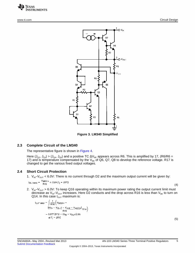
Figure 3. LM340 Simplified
2.3 Complete Circuit of the LM340
The representative figure is shown in Figure 4.
Here (JQ2, JQ3) > (JQ4, JQ5) and a positive TC ΔVBE appears across R6. This is amplified by 17, (R6/R6 =17) and is temperature compensated by the VBE of Q6, Q7, Q8 to develop the reference voltage. R17 ischanged to get the various fixed output voltages.
2.4 Short Circuit Protection1. VIN–VOUT < 6.0V: There is no current through D2 and the maximum output current will be given by:
(4)
2. VIN–VOUT > 6.0V: To keep Q16 operating within its maximum power rating the output current limit mustdecrease as VIN–VOUT increases. Here D2 conducts and the drop across R16 is less than VBE to turn onQ14. In this case IOUT maximum is:
(5)
5SNOA660A–May 2004–Revised Mat 2013 AN-103 LM340 Series Three Terminal Positive RegulatorsSubmit Documentation Feedback
Copyright © 2004–2013, Texas Instruments Incorporated

Circuit Design www.ti.com
*Series pass element†Starting up resistor
Figure 4. Complete Circuit of the LM340
2.5 Thermal Shut Down
In Figure 4 the VBE of Q13 is clamped to 0.4V. When the die temperature reaches approximately +175°Cthe VBE to turn on Q13 is 0.4V. When Q13 turns on it removes all base drive from Q15 which turns off theregulator thus preventing a further increase in die temperature.
2.6 Power Dissipation
The maximum power dissipation of the LM340 is given by:PD MAX = (VIN MAX − VOUT) IOUT MAX +V IN MAX IQ (W) (6)
The maximum junction temperature (assuming that there is no thermal protection) is given by:
(7)
6 AN-103 LM340 Series Three Terminal Positive Regulators SNOA660A–May 2004–Revised Mat 2013Submit Documentation Feedback
Copyright © 2004–2013, Texas Instruments Incorporated

www.ti.com Current Source
Example:
VIN MAX = 23V, IOUT MAX = 1.0A, LM340T-15.
Equation Equation 7 yields: TjM = 200°C. So the Tj max of 150°C specified in the data sheet should be thelimiting temperature.
From Equation 6 PD ≃ 8.1W. The thermal resistance of the heat sink can be estimated from:
(8)
The thermal resistance θj-c (junction to case) of the TO-220 package is 6°C/W, and assuming a θc-s (caseto heat sink) of 0.4, equation Equation 8 yields:
θs-a = 8.4°C/W
3 Current Source
The circuit shown on Figure 5 provides a constant output current (equal to VOUT/R1 or 200 mA) for avariable load impedance of 0 to 85Ω. Using the following definitions and the notation shown on Figure 5,ZOUT and IOUT are:
*Required if regulator is located far from power supply filter
Figure 5. Current Source
QCC/V = Quiescent current change per volt of input/output (pin 1 to pin 2) voltage change of the LM340
Lr/V = Line regulation per volt: the change in the LM340 output voltage per volt of input/output voltagechange at a given IOUT.
(9)
(10)
(11)
(12)
The LM340-5.0 data sheet lists maximum quiescent current change of 1.0 mA for a 7.0V to 25V change ininput voltage; and a line regulation (interpolated for IOUT = 200 mA) of 35 mV maximum for a 7.0V to 25Vchange in input voltage:
7SNOA660A–May 2004–Revised Mat 2013 AN-103 LM340 Series Three Terminal Positive RegulatorsSubmit Documentation Feedback
Copyright © 2004–2013, Texas Instruments Incorporated
High Current Regulator with Short Circuit Current Limit www.ti.com
(13)
(14)
The worst case change in the 200 mA output current for a 1.0V change in output or input voltage usingequation Equation 9 is:
(15)
and the output impedance for a 0 to 85Ω change in ZL using equation Equation 12 is:
(16)
Typical measured values of ZOUT varied from 10–12.3 kΩ, or 81–100 μA/V change input or output(approximately 0.05%/V).
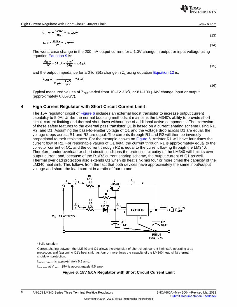
4 High Current Regulator with Short Circuit Current Limit
The 15V regulator circuit of Figure 6 includes an external boost transistor to increase output currentcapability to 5.0A. Unlike the normal boosting methods, it maintains the LM340's ability to provide shortcircuit current limiting and thermal shut-down without use of additional active components. The extensionof these safety features to the external pass transistor Q1 is based on a current sharing scheme using R1,R2, and D1. Assuming the base-to-emitter voltage of Q1 and the voltage drop across D1 are equal, thevoltage drops across R1 and R2 are equal. The currents through R1 and R2 will then be inverselyproportional to their resistances. For the example shown on Figure 6, resistor R1 will have four times thecurrent flow of R2. For reasonable values of Q1 beta, the current through R1 is approximately equal to thecollector current of Q1; and the current through R2 is equal to the current flowing through the LM340.Therefore, under overload or short circuit conditions the protection circuitry of the LM340 will limit its ownoutput current and, because of the R1/R2 current sharing scheme, the output current of Q1 as well.Thermal overload protection also extends Q1 when its heat sink has four or more times the capacity of theLM340 heat sink. This follows from the fact that both devices have approximately the same input/outputvoltage and share the load current in a ratio of four to one.
*Solid tantalum
Current sharing between the LM340 and Q1 allows the extension of short circuit current limit, safe operating areaprotection, and (assuming Q1's heat sink has four or more times the capacity of the LM340 head sink) thermalshutdown protection.
ISHORT CIRCUIT is approximately 5.5 amp.
IOUT MAX at VOUT = 15V is approximately 9.5 amp.
Figure 6. 15V 5.0A Regulator with Short Circuit Current Limit
8 AN-103 LM340 Series Three Terminal Positive Regulators SNOA660A–May 2004–Revised Mat 2013Submit Documentation Feedback
Copyright © 2004–2013, Texas Instruments Incorporated

www.ti.com High Current Regulator with Short Circuit Current Limit
The circuit shown on Figure 6 normally operates at up to 5.0A of output current. This means up to 1.0A ofcurrent flows through the LM340 and up to 4.0A flows through Q1. For short term overload conditions thecurve of Figure 7 shows the maximum instantaneous output current versus temperature for the boostedregulator. This curve reflects the approximately 2.0A current limit of the LM340 causing an 8.0A currentlimit in the pass transistor, or 10A, total.
Figure 7. Maximum Instantaneous Current vs Junction Temperature
Under continuous short circuit conditions the LM340 will heat up and limit to a steady total state shortcircuit current of 4.0A to 6.0A as shown in Figure 8. This curve was taken using a Wakefield 680-75 heatsink (approximately 7.5°C/W) at a 25°C ambient temperature.
Figure 8. Continuous Short CircuitCurrent vs Input Voltage
For optimum current sharing over temperature between the LM340 and Q1, the diode D1 should bephysically located close to the pass transistor on the heat sink in such a manner as to keep it at the sametemperature as that of Q1. If the LM340 and Q1 are mounted on the same heat sink the LM340 should beelectrically isolated from the heat sink since its case (pin 3) is at ground potential and the case of Q1 (itscollector) is at the output potential of the regulator. Capacitors C1 and C2 are required to preventoscillations and improve the output impedance respectively. Resistor R3 provides a path to unloadexcessive base charge from the base of Q1 when the regulator goes suddenly from full load to no load.The single point ground system shown on Figure 6 allows the sense pins (2 and 3) of the LM340 tomonitor the voltage directly at the load rather than at some point along a (possibly) resistive ground returnline carrying up to 5.0A of load current. Figure 9 shows the typical variation of load regulation versus loadcurrent for the boosted regulator. The insertion of the external pass transistor increases the input/outputdifferential voltage from 2.0V to approximately 4.5V. For an output current less than 5.0A, the R2/R1 ratiocan be set lower than 4:1. Therefore, a less expensive PNP transistor may be used.
9SNOA660A–May 2004–Revised Mat 2013 AN-103 LM340 Series Three Terminal Positive RegulatorsSubmit Documentation Feedback
Copyright © 2004–2013, Texas Instruments Incorporated

5.0V, 5.0A Voltage Regulator for TTL www.ti.com
Figure 9. Load Regulation
5 5.0V, 5.0A Voltage Regulator for TTL
The high current 5.0V regulator for TTL shown in Figure 11 uses a relatively inexpensive NPN passtransistor with a lower power PNP device to replace the single, higher cost, power PNP shown in Figure 6.This circuit provides a 5.0V output at up to 5.0A of load current with a typical load regulation of 1.8% fromno load to full load. The peak instantaneous output current observed was 10.4A at a 25°C junctiontemperature (pulsed load with a 1.0 ms ON and a 200 ms OFF period) and 8.4A for a continuous shortcircuit. The typical line regulation is 0.02% of input voltage change (IOUT = 0).
One can easily add an overload indicator using the new NSL5027 LED. This is shown with dotted lines inFigure 11. With this configuration R2 is not only a current sharing resistor but also an overload sensor. R5will determine the current through the LED; the diode D2 has been added to match the drop across D1.Once the load current exceeds 5.0A (1.0A through the LM340 assuming perfect current sharing and VD1 =VD2) Q3 turns ON and the overload indicator lights up.
Example:
IOVERLOAD = 5.0A
ILED = 40 mA (light intensity of 16 mcd)
(17)
6 Adjustable Output Voltage Regulator for Intermediate Output Voltages
The addition of two resistors to an LM340 circuit allows a non-standard output voltage while maintainingthe limiting features built into IC. The example shown in Figure 10 provides a 10V output using anLM340K-5.0 by raising the reference (pin number 3) of the regulator by 5.0V.
Figure 10. 10V Regulator
10 AN-103 LM340 Series Three Terminal Positive Regulators SNOA660A–May 2004–Revised Mat 2013Submit Documentation Feedback
Copyright © 2004–2013, Texas Instruments Incorporated

www.ti.com Adjustable Output Voltage Regulator for Intermediate Output Voltages
The 5.0V pedestal results from the sum of regulator quiescent current IQ and a current equal to VREG/R1,flowing through potentiometer R2 to ground. R2 is made adjustable to compensate for differences in IQand VREG output. The circuit is practical because the change in IQ due to line voltage and load currentchanges is quite small.
*Solid tantalum
Figure 11. 5.0V, 5.0A Regulator for TTL (with short circuit, thermal shutdown protection, and overloadindicator)
The line regulation for the boosted regulator is the sum of the LM340 line regulation, its effects on thecurrent through R2, and the effects of ΔIQ in response to input voltage changes. The change in outputvoltage is:
+ (QCC/V) ΔVIN R2 (18)
giving a total line regulation of:
(19)
The LM340-5.0 data sheet lists ΔVOUT < 50 mV and ΔIQ < 1.0 mA for ΔVIN = 18V at IOUT = 500 mA. This is:
(20)
(21)
The worst case at line regulation for the circuit of Figure 10 calculated by equation Equation 19, IOUT = 500mA and R2 = 310Ω is:
+ (55 µA/V)310Ω (22)
(23)
This represents a worst case line regulation value of 0.23%/V.
The load regulation is the sum of the LM340 voltage regulation, its effect on the current through R2, andthe effect of ΔIQ in response to changes in load current. Using the following definitions and the notationshown on Figure 10 ΔVOUT is:
ZOUT = Regulator output impedance: the change in output voltage per amp of load current change.
11SNOA660A–May 2004–Revised Mat 2013 AN-103 LM340 Series Three Terminal Positive RegulatorsSubmit Documentation Feedback
Copyright © 2004–2013, Texas Instruments Incorporated

Variable Output Regulator www.ti.com
Z340 = LM340 output impedance
QCC/A= Quiescent current change per amp of load current change
(+ QCC/A) ΔIL R2 (24)
and the total output impedance is:
+(QCC/A) R2 (25)
The LM340-5.0 data sheet gives a maximum load regulation Lr = 50 mV and ΔIQ = 1.0 mA for a 1.0A loadchange.
(26)
This gives a worst case dc output impedance (ac output impedance being a function of C2) for the 10Vregulator using equation of:
+ (100 μA/A) 310Ω (27)
ZOUT = 0.10Ω + 0.031Ω = 0.13Ω
or a worst case change of approximately 1.5% for a 1.0A load change. Typical measured values are aboutone-third of the worst case value.
7 Variable Output Regulator
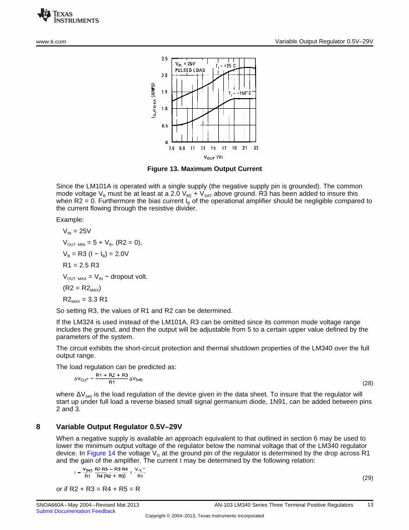
In Figure 12 the ground terminal of the regulator is “lifted” by an amount equal to the voltage applied to thenon-inverting input of the operational amplifier LM101A. The output voltage of the regulator is thereforeraised to a level set by the value of the resistive divider R1, R2, R3 and limited by the input voltage. Withthe resistor values shown in Figure 12, the output voltage is variable from 7.0V to 23V and the maximumoutput current (pulsed load) varies from 1.2A to 2.0A (Tj = 25°C) as shown in Figure 13.
*Required if the regulator is located far from the power supply filter**Solid tantalum
Figure 12. Variable Output Regulator
12 AN-103 LM340 Series Three Terminal Positive Regulators SNOA660A–May 2004–Revised Mat 2013Submit Documentation Feedback
Copyright © 2004–2013, Texas Instruments Incorporated
www.ti.com Variable Output Regulator 0.5V–29V
Figure 13. Maximum Output Current
Since the LM101A is operated with a single supply (the negative supply pin is grounded). The commonmode voltage VB must be at least at a 2.0 VBE + VSAT above ground. R3 has been added to insure thiswhen R2 = 0. Furthermore the bias current IB of the operational amplifier should be negligible compared tothe current flowing through the resistive divider.
Example:
VIN = 25V
VOUT MIN = 5 + VB, (R2 = 0),
VB = R3 (I − IB) = 2.0V
R1 = 2.5 R3
VOUT MAX = VIN − dropout volt.
(R2 = R2MAX)
R2MAX = 3.3 R1
So setting R3, the values of R1 and R2 can be determined.
If the LM324 is used instead of the LM101A, R3 can be omitted since its common mode voltage rangeincludes the ground, and then the output will be adjustable from 5 to a certain upper value defined by theparameters of the system.
The circuit exhibits the short-circuit protection and thermal shutdown properties of the LM340 over the fulloutput range.
The load regulation can be predicted as:
(28)
where ΔV340 is the load regulation of the device given in the data sheet. To insure that the regulator willstart up under full load a reverse biased small signal germanium diode, 1N91, can be added between pins2 and 3.
8 Variable Output Regulator 0.5V–29V
When a negative supply is available an approach equivalent to that outlined in section 6 may be used tolower the minimum output voltage of the regulator below the nominal voltage that of the LM340 regulatordevice. In Figure 14 the voltage VG at the ground pin of the regulator is determined by the drop across R1and the gain of the amplifier. The current I may be determined by the following relation:
(29)
or if R2 + R3 = R4 + R5 = R
13SNOA660A–May 2004–Revised Mat 2013 AN-103 LM340 Series Three Terminal Positive RegulatorsSubmit Documentation Feedback
Copyright © 2004–2013, Texas Instruments Incorporated

Variable Output Regulator 0.5V–29V www.ti.com
(30)
*Solid tantalum
Figure 14. Variable Output Voltage 0.5V−30V
considering that the output is given by:VOUT = VG + V340 (31)
andVG = R1 I − VIN
− (32)
combining equations 31, 32, and 33 an expression for the output voltage is:
(33)
Notice that the output voltage is inversely proportional to R4 so the output voltage may be adjusted veryaccurately for low values. A minimum output of 0.5V has been set. This implies that
(34)
An absolute zero output voltage will require R4 = ∞ or R2 = 0, neither being practical in this circuit. Themaximum output voltage as shown in Figure 14 is 30V if the high voltage operational amplifier LM143 isused. If only low values of VOUT are sought, then an LM101 may be used. R1 can be computed from:
(35)
14 AN-103 LM340 Series Three Terminal Positive Regulators SNOA660A–May 2004–Revised Mat 2013Submit Documentation Feedback
Copyright © 2004–2013, Texas Instruments Incorporated

www.ti.com Dual Power Supply
Figure 15. Typical Load Regulation for a 0.5V−30VRegulator (ΔIOUT = 1.0A)
Figure 15 illustrates the load regulation as a function of the output voltage.
9 Dual Power Supply
The plus and minus regulators shown in Figure 16 will exhibit line and load regulations consistent withtheir specifications as individual regulators. In fact, operation will be entirely normal until the problem ofcommon loads occurs. A 30Ω load from the +15V output to the −15V output (representing a 0.5A startingload for the LM340K-15 if the LM320K-15 is already started) would allow start up of the LM340 in mostcases. To insure LM340 startup over the full temperature range into a worst case 1.0A current sink loadthe germanium power “diode” D1 has been added to the circuit. Since the forward voltage drop of thegermanium diode D1 is less than that of the silicon substrate diode of the LM340 the external diode willtake any fault current and allow the LM340 to start up even into a negative voltage load. D1 and silicondiode D2 also protect the regulator outputs from inadvertent shorts between outputs and to ground. Forshorts between outputs the voltage difference between either input and the opposite regulator outputshould not exceed the maximum rating of the device.
The example shown in Figure 16 is a symmetrical ±15V supply for linear circuits. The same principleapplies to non-symmetrical supplies such as a +5.0V and −12V regulator for applications such asregisters.
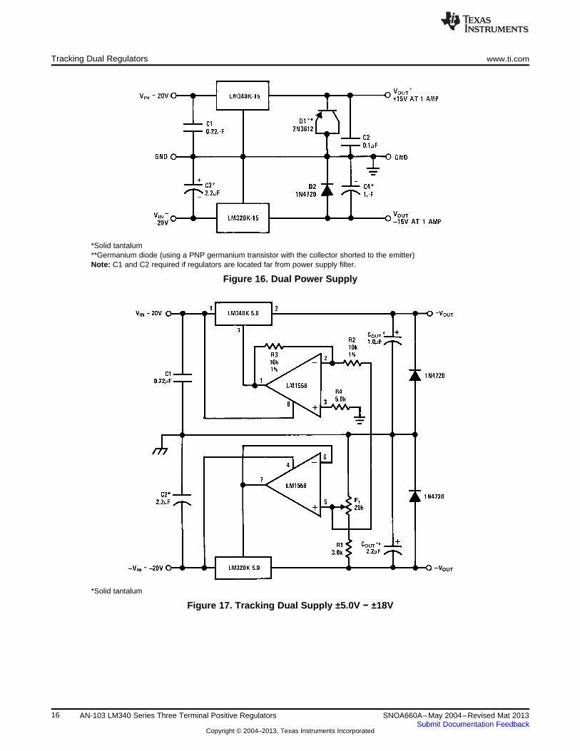
10 Tracking Dual Regulators
In Figure 17, a fraction of the negative output voltage “lifts” the ground pins of the negative LM320K-15voltage regulator and the LM340K-15 through a voltage follower and an inverter respectively. The dualoperational amplifier LM1558 is used for this application and since its supply voltage may go as high as±22V the regulator outputs may be set between 5.0V and 20V. Because of the tighter output tolerance andthe better drift of the LM320, the positive regulator is made to track the negative. The best tracking actionis achieved by matching the gain of both operational amplifiers, that is, the resistors R2 and R3 must bematched as closely as possible.
15SNOA660A–May 2004–Revised Mat 2013 AN-103 LM340 Series Three Terminal Positive RegulatorsSubmit Documentation Feedback
Copyright © 2004–2013, Texas Instruments Incorporated
Tracking Dual Regulators www.ti.com
*Solid tantalum**Germanium diode (using a PNP germanium transistor with the collector shorted to the emitter)Note: C1 and C2 required if regulators are located far from power supply filter.
Figure 16. Dual Power Supply
*Solid tantalum
Figure 17. Tracking Dual Supply ±5.0V − ±18V
16 AN-103 LM340 Series Three Terminal Positive Regulators SNOA660A–May 2004–Revised Mat 2013Submit Documentation Feedback
Copyright © 2004–2013, Texas Instruments Incorporated
www.ti.com High Input Voltage
*Germanium diode**Solid tantalum
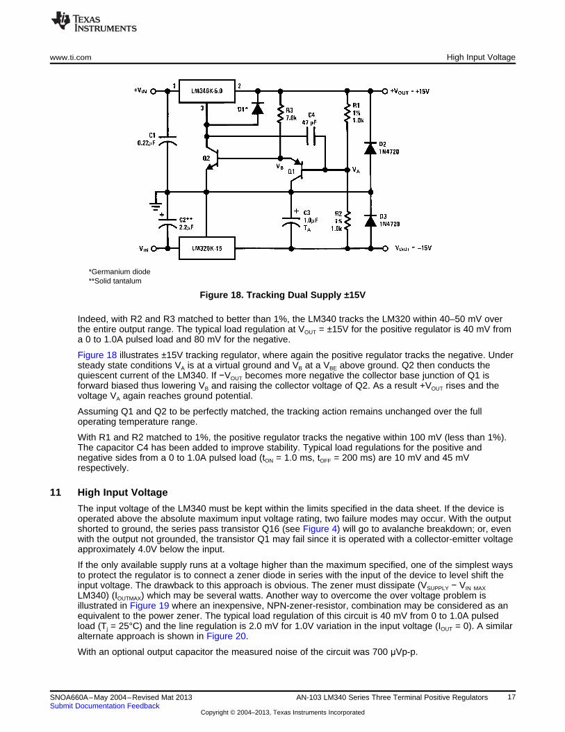
Figure 18. Tracking Dual Supply ±15V
Indeed, with R2 and R3 matched to better than 1%, the LM340 tracks the LM320 within 40–50 mV overthe entire output range. The typical load regulation at VOUT = ±15V for the positive regulator is 40 mV froma 0 to 1.0A pulsed load and 80 mV for the negative.
Figure 18 illustrates ±15V tracking regulator, where again the positive regulator tracks the negative. Understeady state conditions VA is at a virtual ground and VB at a VBE above ground. Q2 then conducts thequiescent current of the LM340. If −VOUT becomes more negative the collector base junction of Q1 isforward biased thus lowering VB and raising the collector voltage of Q2. As a result +VOUT rises and thevoltage VA again reaches ground potential.
Assuming Q1 and Q2 to be perfectly matched, the tracking action remains unchanged over the fulloperating temperature range.
With R1 and R2 matched to 1%, the positive regulator tracks the negative within 100 mV (less than 1%).The capacitor C4 has been added to improve stability. Typical load regulations for the positive andnegative sides from a 0 to 1.0A pulsed load (tON = 1.0 ms, tOFF = 200 ms) are 10 mV and 45 mVrespectively.
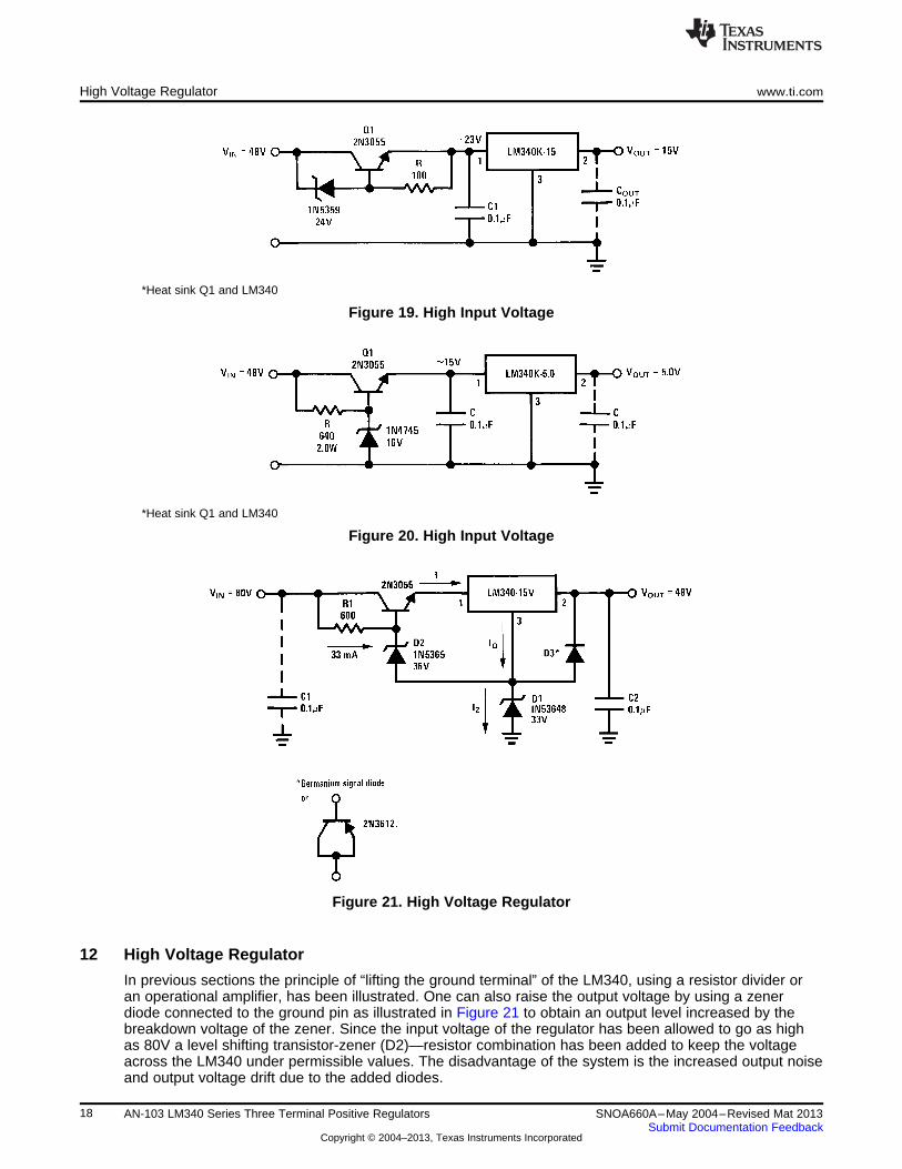
11 High Input Voltage
The input voltage of the LM340 must be kept within the limits specified in the data sheet. If the device isoperated above the absolute maximum input voltage rating, two failure modes may occur. With the outputshorted to ground, the series pass transistor Q16 (see Figure 4) will go to avalanche breakdown; or, evenwith the output not grounded, the transistor Q1 may fail since it is operated with a collector-emitter voltageapproximately 4.0V below the input.
If the only available supply runs at a voltage higher than the maximum specified, one of the simplest waysto protect the regulator is to connect a zener diode in series with the input of the device to level shift theinput voltage. The drawback to this approach is obvious. The zener must dissipate (VSUPPLY − VIN MAX
LM340) (IOUTMAX) which may be several watts. Another way to overcome the over voltage problem isillustrated in Figure 19 where an inexpensive, NPN-zener-resistor, combination may be considered as anequivalent to the power zener. The typical load regulation of this circuit is 40 mV from 0 to 1.0A pulsedload (Tj = 25°C) and the line regulation is 2.0 mV for 1.0V variation in the input voltage (IOUT = 0). A similaralternate approach is shown in Figure 20.
With an optional output capacitor the measured noise of the circuit was 700 μVp-p.
17SNOA660A–May 2004–Revised Mat 2013 AN-103 LM340 Series Three Terminal Positive RegulatorsSubmit Documentation Feedback
Copyright © 2004–2013, Texas Instruments Incorporated
High Voltage Regulator www.ti.com
*Heat sink Q1 and LM340
Figure 19. High Input Voltage
*Heat sink Q1 and LM340
Figure 20. High Input Voltage
Figure 21. High Voltage Regulator
12 High Voltage Regulator
In previous sections the principle of “lifting the ground terminal” of the LM340, using a resistor divider oran operational amplifier, has been illustrated. One can also raise the output voltage by using a zenerdiode connected to the ground pin as illustrated in Figure 21 to obtain an output level increased by thebreakdown voltage of the zener. Since the input voltage of the regulator has been allowed to go as highas 80V a level shifting transistor-zener (D2)—resistor combination has been added to keep the voltageacross the LM340 under permissible values. The disadvantage of the system is the increased output noiseand output voltage drift due to the added diodes.
18 AN-103 LM340 Series Three Terminal Positive Regulators SNOA660A–May 2004–Revised Mat 2013Submit Documentation Feedback
Copyright © 2004–2013, Texas Instruments Incorporated

www.ti.com Electronic Shutdown
Indeed it can be seen that, from no load to full load conditions, the ΔlZ will be approximately the currentthrough R1 (≃ 35 mA) and therefore the degraded regulation caused by D1 will be VZ (at 35 mA + lQ) − VZ
(at lQ).
The measured load regulation was 60 mV for ΔlOUT of 5.0 mA to 1.0A (pulsed load), and the lineregulation is 0.01%V of input voltage change (lOUT = 500 mA) and the typical output noise 2.0 mVp-p (C2 =0.1 μF). The value of R1 is calculated as:
(36)
13 Electronic Shutdown
Figure 22 shows a practical method of shutting down the LM340 under the control of a TTL or DTL logicgate. The pass transistor Q1 operates either as a saturated transistor or as an open switch. With the logicinput high (2.4V specified minimum for TTL logic) transistor Q2 turns on and pulls 50 mA down throughR2. This provides sufficient base drive to maintain Q1 in saturation during the ON condition of the switch.When the logic input is low (0.4V specified maximum for TTL logic) Q2 is held off, as is Q1; and the switchis in the OFF condition. The observed turn-on time was 7.0 μs for resistive loads from 15Ω to infinity andthe turn-off time varied from approximately 3.0 μs for a 15Ω load to 3.0 ms for a no-load condition. Turn-off time is controlled primarily by the time constant of RLOAD and C1.
*Required if the regulator is located far from the power supply filter**Head sink Q1 and the LM340
Figure 22. Electronic Shutdown Circuit
19SNOA660A–May 2004–Revised Mat 2013 AN-103 LM340 Series Three Terminal Positive RegulatorsSubmit Documentation Feedback
Copyright © 2004–2013, Texas Instruments Incorporated
Variable High Voltage Regulator with Overvoltage Shutdown www.ti.com
*Solid tantalum
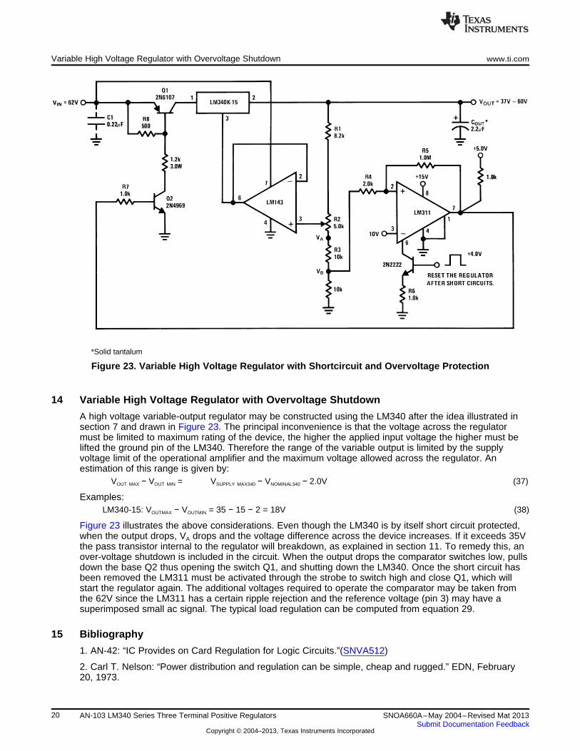
Figure 23. Variable High Voltage Regulator with Shortcircuit and Overvoltage Protection
14 Variable High Voltage Regulator with Overvoltage Shutdown
A high voltage variable-output regulator may be constructed using the LM340 after the idea illustrated insection 7 and drawn in Figure 23. The principal inconvenience is that the voltage across the regulatormust be limited to maximum rating of the device, the higher the applied input voltage the higher must belifted the ground pin of the LM340. Therefore the range of the variable output is limited by the supplyvoltage limit of the operational amplifier and the maximum voltage allowed across the regulator. Anestimation of this range is given by:
VOUT MAX − VOUT MIN = VSUPPLY MAX340 − VNOMINAL340 − 2.0V (37)
Examples:LM340-15: VOUTMAX − VOUTMIN = 35 − 15 − 2 = 18V (38)
Figure 23 illustrates the above considerations. Even though the LM340 is by itself short circuit protected,when the output drops, VA drops and the voltage difference across the device increases. If it exceeds 35Vthe pass transistor internal to the regulator will breakdown, as explained in section 11. To remedy this, anover-voltage shutdown is included in the circuit. When the output drops the comparator switches low, pullsdown the base Q2 thus opening the switch Q1, and shutting down the LM340. Once the short circuit hasbeen removed the LM311 must be activated through the strobe to switch high and close Q1, which willstart the regulator again. The additional voltages required to operate the comparator may be taken fromthe 62V since the LM311 has a certain ripple rejection and the reference voltage (pin 3) may have asuperimposed small ac signal. The typical load regulation can be computed from equation 29.
15 Bibliography
1. AN-42: “IC Provides on Card Regulation for Logic Circuits.”(SNVA512)
2. Carl T. Nelson: “Power distribution and regulation can be simple, cheap and rugged.” EDN, February20, 1973.
20 AN-103 LM340 Series Three Terminal Positive Regulators SNOA660A–May 2004–Revised Mat 2013Submit Documentation Feedback
Copyright © 2004–2013, Texas Instruments Incorporated
IMPORTANT NOTICE
Texas Instruments Incorporated and its subsidiaries (TI) reserve the right to make corrections, enhancements, improvements and otherchanges to its semiconductor products and services per JESD46, latest issue, and to discontinue any product or service per JESD48, latestissue. Buyers should obtain the latest relevant information before placing orders and should verify that such information is current andcomplete. All semiconductor products (also referred to herein as “components”) are sold subject to TI’s terms and conditions of salesupplied at the time of order acknowledgment.
TI warrants performance of its components to the specifications applicable at the time of sale, in accordance with the warranty in TI’s termsand conditions of sale of semiconductor products. Testing and other quality control techniques are used to the extent TI deems necessaryto support this warranty. Except where mandated by applicable law, testing of all parameters of each component is not necessarilyperformed.
TI assumes no liability for applications assistance or the design of Buyers’ products. Buyers are responsible for their products andapplications using TI components. To minimize the risks associated with Buyers’ products and applications, Buyers should provideadequate design and operating safeguards.
TI does not warrant or represent that any license, either express or implied, is granted under any patent right, copyright, mask work right, orother intellectual property right relating to any combination, machine, or process in which TI components or services are used. Informationpublished by TI regarding third-party products or services does not constitute a license to use such products or services or a warranty orendorsement thereof. Use of such information may require a license from a third party under the patents or other intellectual property of thethird party, or a license from TI under the patents or other intellectual property of TI.
Reproduction of significant portions of TI information in TI data books or data sheets is permissible only if reproduction is without alterationand is accompanied by all associated warranties, conditions, limitations, and notices. TI is not responsible or liable for such altereddocumentation. Information of third parties may be subject to additional restrictions.
Resale of TI components or services with statements different from or beyond the parameters stated by TI for that component or servicevoids all express and any implied warranties for the associated TI component or service and is an unfair and deceptive business practice.TI is not responsible or liable for any such statements.
Buyer acknowledges and agrees that it is solely responsible for compliance with all legal, regulatory and safety-related requirementsconcerning its products, and any use of TI components in its applications, notwithstanding any applications-related information or supportthat may be provided by TI. Buyer represents and agrees that it has all the necessary expertise to create and implement safeguards whichanticipate dangerous consequences of failures, monitor failures and their consequences, lessen the likelihood of failures that might causeharm and take appropriate remedial actions. Buyer will fully indemnify TI and its representatives against any damages arising out of the useof any TI components in safety-critical applications.
In some cases, TI components may be promoted specifically to facilitate safety-related applications. With such components, TI’s goal is tohelp enable customers to design and create their own end-product solutions that meet applicable functional safety standards andrequirements. Nonetheless, such components are subject to these terms.
No TI components are authorized for use in FDA Class III (or similar life-critical medical equipment) unless authorized officers of the partieshave executed a special agreement specifically governing such use.
Only those TI components which TI has specifically designated as military grade or “enhanced plastic” are designed and intended for use inmilitary/aerospace applications or environments. Buyer acknowledges and agrees that any military or aerospace use of TI componentswhich have not been so designated is solely at the Buyer's risk, and that Buyer is solely responsible for compliance with all legal andregulatory requirements in connection with such use.
TI has specifically designated certain components as meeting ISO/TS16949 requirements, mainly for automotive use. In any case of use ofnon-designated products, TI will not be responsible for any failure to meet ISO/TS16949.
Products Applications
Audio www.ti.com/audio Automotive and Transportation www.ti.com/automotive
Amplifiers amplifier.ti.com Communications and Telecom www.ti.com/communications
Data Converters dataconverter.ti.com Computers and Peripherals www.ti.com/computers
DLP® Products www.dlp.com Consumer Electronics www.ti.com/consumer-apps
DSP dsp.ti.com Energy and Lighting www.ti.com/energy
Clocks and Timers www.ti.com/clocks Industrial www.ti.com/industrial
Interface interface.ti.com Medical www.ti.com/medical
Logic logic.ti.com Security www.ti.com/security
Power Mgmt power.ti.com Space, Avionics and Defense www.ti.com/space-avionics-defense
Microcontrollers microcontroller.ti.com Video and Imaging www.ti.com/video
RFID www.ti-rfid.com
OMAP Applications Processors www.ti.com/omap TI E2E Community e2e.ti.com
Wireless Connectivity www.ti.com/wirelessconnectivity
Mailing Address: Texas Instruments, Post Office Box 655303, Dallas, Texas 75265Copyright © 2013, Texas Instruments Incorporated