Embed Size (px)
Citation preview
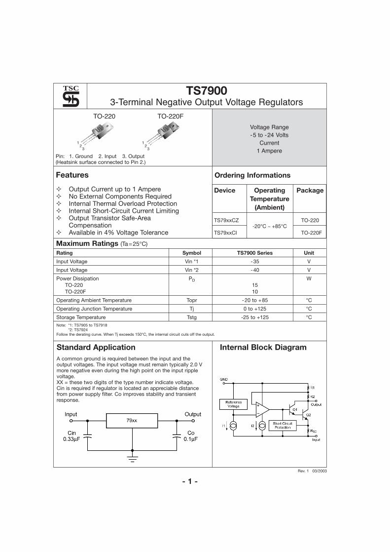
TS79003-Terminal Negative Output Voltage Regulators
Features
Output Current up to 1 AmpereNo External Components RequiredInternal Thermal Overload ProtectionInternal Short-Circuit Current LimitingOutput Transistor Safe-AreaCompensationAvailable in 4% Voltage Tolerance
Voltage Range-5 to -24 Volts
Current1 Ampere
TSC
TO-220
Pin: 1. Ground 2. Input 3. Output(Heatsink surface connected to Pin 2.)
12
3
TO-220F
12
3
- 1 -Rev. 1 03/2003
Ordering Informations
Device Operating PackageTemperature
(Ambient)
TS79xxCZ TO-220
TS79xxCI-20°C ~ +85°C
TO-220F
Rating Symbol TS7900 Series Unit
Input Voltage Vin *1 -35 V
Input Voltage Vin *2 -40 V
Power Dissipation PD WTO-220 15TO-220F 10
Operating Ambient Temperature Topr -20 to +85 °C
Operating Junction Temperature Tj 0 to +125 °C
Storage Temperature Tstg -25 to +125 °C
Maximum Ratings (Ta=25°C)
Note: *1: TS7905 to TS7918*2: TS7924
Follow the derating curve. When Tj exceeds 150°C, the internal circuit cuts off the output.
Standard ApplicationA common ground is required between the input and the output voltages. The input voltage must remain typically 2.0 Vmore negative even during the high point on the input ripplevoltage.XX = these two digits of the type number indicate voltage.Cin is required if regulator is located an appreciable distancefrom power supply filter. Co improves stability and transientresponse.
Internal Block Diagram
- 2 -
TSC
Rev. 1 03/2003
TS7905 Electrical Characteristics (Vin = -10V, Iout = 500mA, Cin = 2µF, Cout = 1µF; Tj = 0°C to 125°C, unless otherwise specified.)Characteristic Symbol Test Circuit Condition Min Typ Max Unit
Output Voltage Vo 1 Tj=25°C -4.80 -5.0 -5.20 V
Output Voltage Tolerance Vo 1 Vi=-7 to -20V, Io=5mA to 1A, -4.75 -5.0 -5.25 VPD<15W
Line Regulation REGline 1 Tj=25°C Vi=-7 to -25V -- 3 100 mV
Vi=-8 to -12V -- 1 50 mV
Load Regulation REGload 1 Tj=25°C Io=5mA to 1.5A -- 10 100 mV
Io=250mA to 750mA -- 3 50 mV
Quiescent Current Iq 3 Tj=25°C -- 2 4 mA
Quiescent Current Change ∆ Iq 3 VIN=-7 to -25V -- -- 1.3 mA
Io=5mA to 1.5A -- -- 0.5 mA
Output Noise Voltage Vn 1 f=10Hz to 100KHz, Ta=25°C -- 40 -- µV
Ripple Rejection Ratio RR 2 Vi=-8 to -18V, Io=100mA, 62 74 -- dBf=120Hz
Min. I/O Voltage Difference Vdif Io=1A, Tj=25°C -- 1.1 -- V
Peak Output Current Io-peak 1 Tj=25°C -- 2.1 -- A
Output Voltage ∆ Vo/Ta 1 Io=5mA, Tj=0 to 125°C -- -0.4 -- mV/°CTemperature Coefficient
TS7906 Electrical Characteristics (Vin = -11V, Iout = 500mA, Cin = 2µF, Cout = 1µF; Tj = 0°C to 125°C, unless otherwise specified.)Characteristic Symbol Test Circuit Condition Min Typ Max Unit
Output Voltage Vo 1 Tj=25°C -5.75 -6.0 -6.25 V
Output Voltage Tolerance Vo 1 Vi=-8 to -21V, Io=5mA to 1A, -5.70 -6.0 -6.30 VPD<15W
Line Regulation REGline 1 Tj=25°C Vi=-8 to -25V -- 4 120 mV
Vi=-9 to -13V -- 1.5 60 mV
Load Regulation REGload 1 Tj=25°C Io=5mA to 1.5A -- 10 120 mV
Io=250mA to 750mA -- 3 60 mV
Quiescent Current Iq 3 Tj=25°C -- 2 4 mA
Quiescent Current Change ∆ Iq 3 Vi=-8 to -25V, Tj=25°C -- -- 1.3 mA
Io=5mA to 1.5A, Tj=25°C -- -- 0.5 mA
Output Noise Voltage Vn 1 f=10Hz to 100KHz, Ta=25°C -- 44 -- µV
Ripple Rejection Ratio RR 2 Vi=-9 to -19V, Io=100mA, 60 73 -- dBf=120Hz
Min. I/O Voltage Difference Vdif Io=1A, Tj=25°C -- 1.1 -- V
Peak Output Current Io-peak 1 Tj=25°C -- 2.1 -- A
Output Voltage ∆ Vo/Ta 1 Io=5mA, Tj=0 to 125°C -- -0.5 -- mV/°CTemperature Coefficient
Note: The specified condition Tj=25°C means that the test should be carried out with the test time so short (within 10mS), that the drift in characteristic value due to the rise in chip junction temperature can be ignored.
- 3 -
TSC
Rev. 1 03/2003
TS7908 Electrical Characteristics (Vin = -14V, Iout = 500mA, Cin = 2µF, Cout = 1µF; Tj = 0°C to 125°C, unless otherwise specified.)Characteristic Symbol Test Circuit Condition Min Typ Max Unit
Output Voltage Vo 1 Tj=25°C -7.69 -8.0 -8.32 V
Output Voltage Tolerance Vo 1 Vi=-10.5 to -23V, -7.61 -8.0 -8.40 VIo=5mA to 1A, PD<15W
Line Regulation REGline 1 Tj=25°C Vi=-10.5 to -25V -- 6 160 mV
Vi=-11 to -17V -- 2 80 mV
Load Regulation REGload 1 Tj=25°C Io=5mA to 1.5A -- 12 160 mV
Io=250mA to 750mA -- 4 80 mV
Quiescent Current Iq 3 Tj=25°C -- 2 4 mA
Quiescent Current Change ∆ Iq 3 Vi=-10.5 to -25V, Tj=25°C -- -- 1 mA
Io=5mA to 1.5A -- -- 0.5 mA
Output Noise Voltage Vn 1 f=10Hz to 100KHz, Ta=25°C -- 52 -- µV
Ripple Rejection Ratio RR 2 Vi=-11 to -21V, Io=100mA, 56 71 -- dBf=120Hz
Min. I/O Voltage Difference Vdif Io=1A, Tj=25°C -- 2 -- V
Peak Output Current Io-peak 1 Tj=25°C -- 2.1 -- A
Output Voltage ∆ Vo/Ta 1 Io=5mA, Tj=0 to 125°C -- -0.6 -- mV/°CTemperature Coefficient
TS7909 Electrical Characteristics (Vin = -15V, Iout = 500mA, Cin = 2µF, Cout = 1µF; Tj = 0°C to 125°C, unless otherwise specified.)Characteristic Symbol Test Circuit Condition Min Typ Max Unit
Output Voltage Vo 1 Tj=25°C -8.65 -9.0 -9.36 V
Output Voltage Tolerance Vo 1 Vi=-11.5 to -24V, -8.57 -9.0 -9.45 VIo=5mA to 1A, PD<15W
Line Regulation REGline 1 Tj=25°C Vi=-11.5 to -26V -- 7 180 mV
Vi=-12 to -18V -- 2 90 mV
Load Regulation REGload 1 Tj=25°C Io=5mA to 1.5A -- 12 180 mV
Io=250mA to 750mA -- 4 90 mV
Quiescent Current Iq 3 Tj=25°C -- 2.2 4.5 mA
Quiescent Current Change ∆ Iq 3 Vi=-11.5 to -26V, Tj=25°C -- -- 1 mA
Io=5mA to 1.5A -- -- 0.5 mA
Output Noise Voltage Vn 1 f=10Hz to 100KHz, Ta=25°C -- 58 -- µV
Ripple Rejection Ratio RR 2 Vi=-12 to -22V, Io=100mA, 56 71 -- dBf=120Hz
Min. I/O Voltage Difference Vdif Io=1A, Tj=25°C -- 1.1 -- V
Peak Output Current Io-peak 1 Tj=25°C -- 2.1 -- A
Output Voltage ∆ Vo/Ta 1 Io=5mA, Tj=0 to 125°C -- -0.6 -- mV/°CTemperature Coefficient
Note: The specified condition Tj=25°C means that the test should be carried out with the test time so short (within 10mS), that the drift in characteristic value due to the rise in chip junction temperature can be ignored.
- 4 -
TSC
Rev. 1 03/2003
TS7912 Electrical Characteristics (Vin = -19V, Iout = 500mA, Cin = 2µF, Cout = 1µF; Tj = 0°C to 125°C, unless otherwise specified.)Characteristic Symbol Test Circuit Condition Min Typ Max Unit
Output Voltage Vo 1 Tj=25°C -11.53 -12 -12.48 V
Output Voltage Tolerance Vo 1 Vi=-14.5 to -27V, -11.42 -12 -12.60 VIo=5mA to 1A, PD<15W
Line Regulation REGline 1 Tj=25°C Vi=-14.5 to -30V -- 10 240 mV
Vi=-16 to -22V -- 3 120 mV
Load Regulation REGload 1 Tj=25°C Io=5mA to 1.5A -- 12 240 mV
Io=250mA to 750mA -- 4 120 mV
Quiescent Current Iq 3 Tj=25°C -- 2.5 5 mA
Quiescent current Change ∆ Iq 3 Vi=-14.5 to -30V, Tj=25°C -- -- 1 mA
Io=5mA to 1.5A -- -- 0.5 mA
Output Noise Voltage Vn 1 f=10Hz to 100KHz, Ta=25°C -- 75 -- µV
Ripple Rejection Ratio RR 2 Vi=-15 to -25V, Io=100mA, 55 70 -- dBf=120Hz
Min. I/O Voltage Difference Vdif Io=1A, Tj=25°C -- 1.1 -- V
Peak Output Current Io-peak 1 Tj=25°C -- 2.1 -- A
Output Voltage ∆ Vo/Ta 1 Io=5mA, Tj=0 to 125°C -- -0.8 -- mV/°CTemperature Coefficient
TS7915 Electrical Characteristics (Vin = -23V, Iout = 500mA, Cin = 2µF, Cout = 1µF; Tj = 0°C to 125°C, unless otherwise specified.)Characteristic Symbol Test Circuit Condition Min Typ Max Unit
Output Voltage Vo 1 Tj=25°C -14.42 -15 -15.60 V
Output Voltage Tolerance Vo 1 Vi=-17.5 to -30V, -14.28 -15 -15.75 VIo=5mA to 1A, PD<15W
Line Regulation REGline 1 Tj=25°C Vi=-17.5 to -30V -- 11 300 mV
Vi=-20 to -26V -- 3 150 mV
Load Regulation REGload 1 Tj=25°C Io=5mA to 1.5A -- 12 300 mV
Io=250mA to 750mA -- 4 150 mV
Quiescent Current Iq 3 Tj=25°C -- 2.5 5 mA
Quiescent current Change ∆ Iq 3 Vi=-17.5 to -30V -- -- 1 mA
Io=5mA to 1.5A -- -- 0.5 mA
Output Noise Voltage Vn 1 f=10Hz to 100KHz, Ta=25°C -- 90 -- µV
Ripple Rejection Ratio RR 2 Vi=-18.5 to -28.5V, 54 69 -- dBIo=100mA, f=120Hz
Min. I/O Voltage Difference Vdif Io=1A, Tj=25°C -- 1.1 -- V
Peak Output Current Io-peak 1 Tj=25°C -- 2.1 -- A
Output Voltage ∆ Vo/Ta 1 Io=5mA, Tj=0 to 125°C -- -0.9 -- mV/°CTemperature Coefficient
Note: The specified condition Tj=25°C means that the test should be carried out with the test time so short (within 10mS), that the drift in characteristic value due to the rise in chip junction temperature can be ignored.
- 5 -
TSC
Rev. 1 03/2003
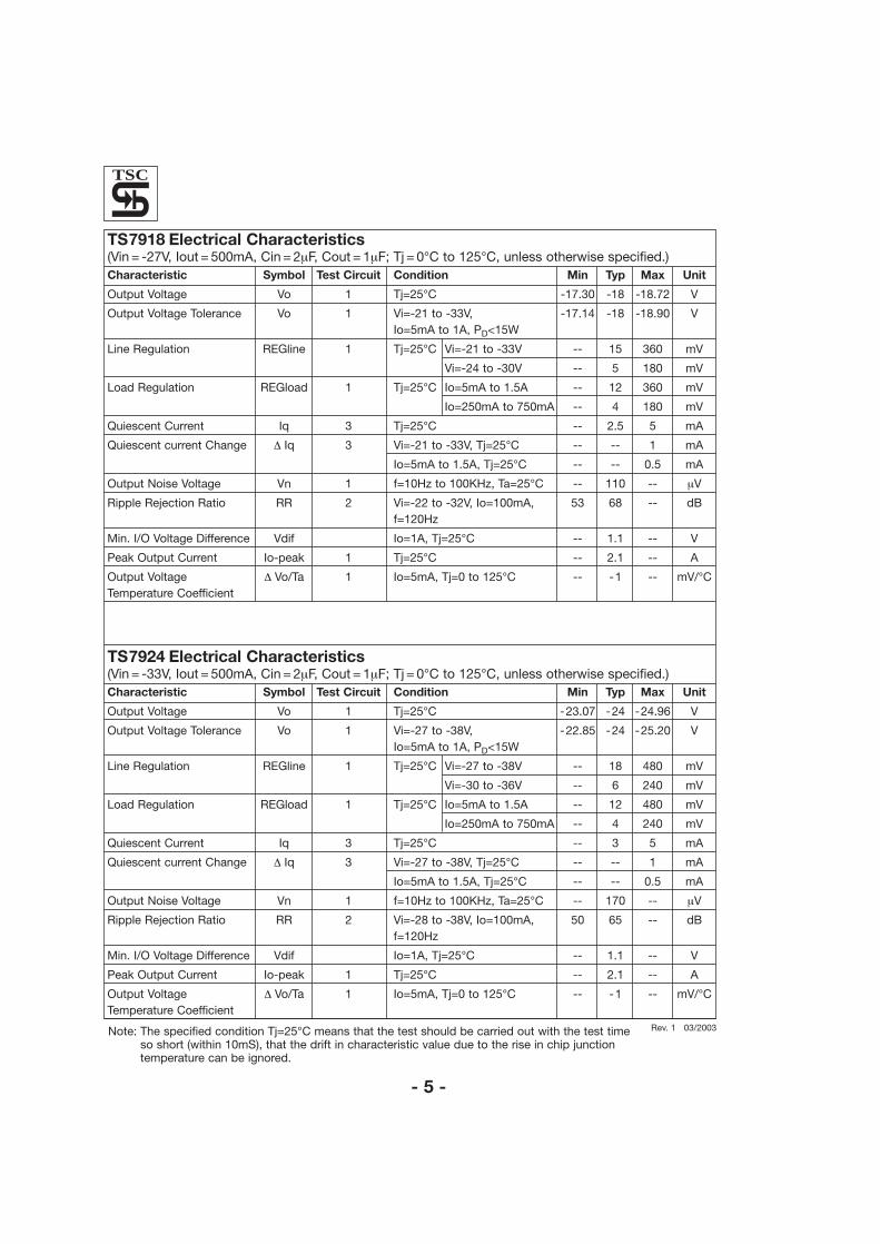
TS7918 Electrical Characteristics (Vin = -27V, Iout = 500mA, Cin = 2µF, Cout = 1µF; Tj = 0°C to 125°C, unless otherwise specified.)Characteristic Symbol Test Circuit Condition Min Typ Max Unit
Output Voltage Vo 1 Tj=25°C -17.30 -18 -18.72 V
Output Voltage Tolerance Vo 1 Vi=-21 to -33V, -17.14 -18 -18.90 VIo=5mA to 1A, PD<15W
Line Regulation REGline 1 Tj=25°C Vi=-21 to -33V -- 15 360 mV
Vi=-24 to -30V -- 5 180 mV
Load Regulation REGload 1 Tj=25°C Io=5mA to 1.5A -- 12 360 mV
Io=250mA to 750mA -- 4 180 mV
Quiescent Current Iq 3 Tj=25°C -- 2.5 5 mA
Quiescent current Change ∆ Iq 3 Vi=-21 to -33V, Tj=25°C -- -- 1 mA
Io=5mA to 1.5A, Tj=25°C -- -- 0.5 mA
Output Noise Voltage Vn 1 f=10Hz to 100KHz, Ta=25°C -- 110 -- µV
Ripple Rejection Ratio RR 2 Vi=-22 to -32V, Io=100mA, 53 68 -- dBf=120Hz
Min. I/O Voltage Difference Vdif Io=1A, Tj=25°C -- 1.1 -- V
Peak Output Current Io-peak 1 Tj=25°C -- 2.1 -- A
Output Voltage ∆ Vo/Ta 1 Io=5mA, Tj=0 to 125°C -- -1 -- mV/°CTemperature Coefficient
TS7924 Electrical Characteristics (Vin = -33V, Iout = 500mA, Cin = 2µF, Cout = 1µF; Tj = 0°C to 125°C, unless otherwise specified.)Characteristic Symbol Test Circuit Condition Min Typ Max Unit
Output Voltage Vo 1 Tj=25°C -23.07 -24 -24.96 V
Output Voltage Tolerance Vo 1 Vi=-27 to -38V, -22.85 -24 -25.20 VIo=5mA to 1A, PD<15W
Line Regulation REGline 1 Tj=25°C Vi=-27 to -38V -- 18 480 mV
Vi=-30 to -36V -- 6 240 mV
Load Regulation REGload 1 Tj=25°C Io=5mA to 1.5A -- 12 480 mV
Io=250mA to 750mA -- 4 240 mV
Quiescent Current Iq 3 Tj=25°C -- 3 5 mA
Quiescent current Change ∆ Iq 3 Vi=-27 to -38V, Tj=25°C -- -- 1 mA
Io=5mA to 1.5A, Tj=25°C -- -- 0.5 mA
Output Noise Voltage Vn 1 f=10Hz to 100KHz, Ta=25°C -- 170 -- µV
Ripple Rejection Ratio RR 2 Vi=-28 to -38V, Io=100mA, 50 65 -- dBf=120Hz
Min. I/O Voltage Difference Vdif Io=1A, Tj=25°C -- 1.1 -- V
Peak Output Current Io-peak 1 Tj=25°C -- 2.1 -- A
Output Voltage ∆ Vo/Ta 1 Io=5mA, Tj=0 to 125°C -- -1 -- mV/°CTemperature Coefficient
Note: The specified condition Tj=25°C means that the test should be carried out with the test time so short (within 10mS), that the drift in characteristic value due to the rise in chip junction temperature can be ignored.
- 6 -
TSC
Rev. 1 03/2003
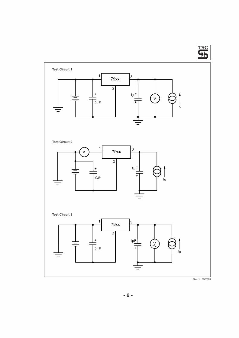
Test Circuit 1
Test Circuit 2
Test Circuit 3
- 7 -
TSC
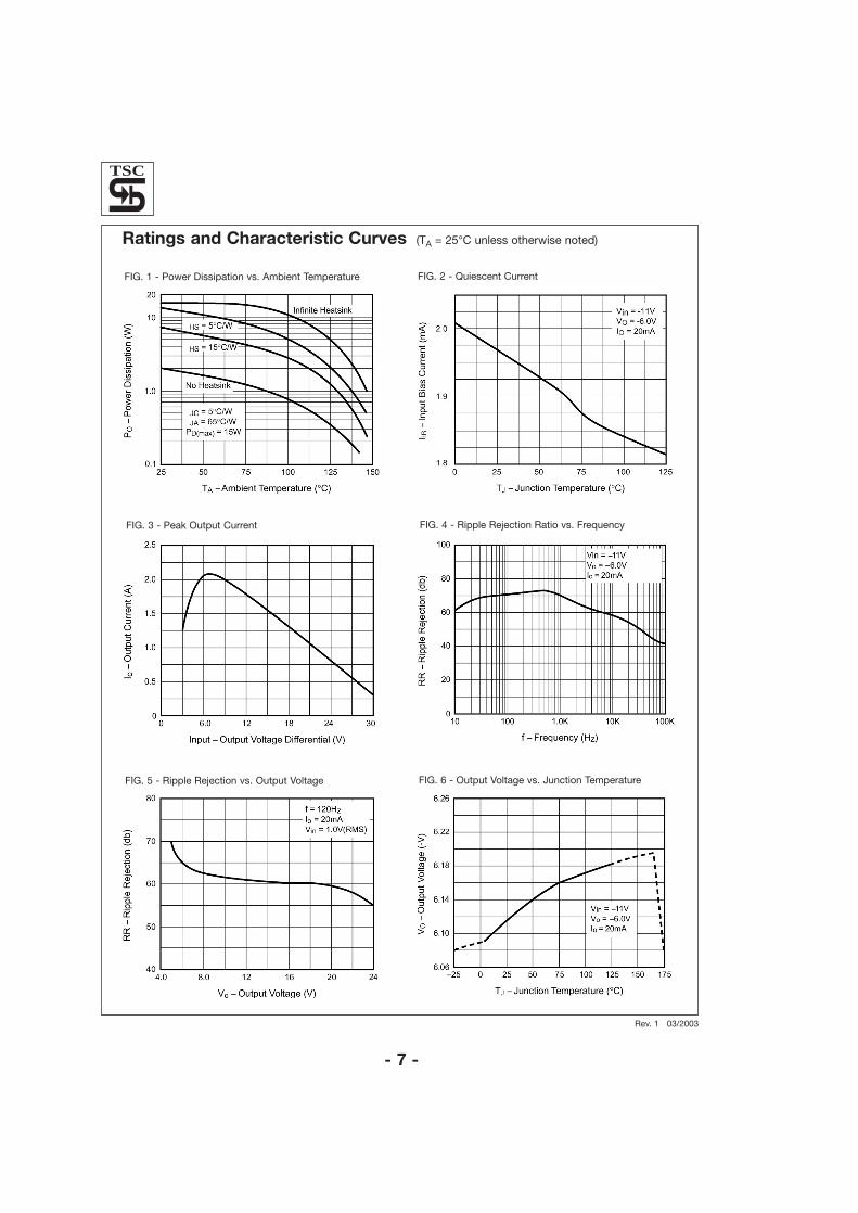
FIG. 1 - Power Dissipation vs. Ambient Temperature FIG. 2 - Quiescent Current
FIG. 3 - Peak Output Current FIG. 4 - Ripple Rejection Ratio vs. Frequency
FIG. 5 - Ripple Rejection vs. Output Voltage FIG. 6 - Output Voltage vs. Junction Temperature
Rev. 1 03/2003
Ratings and Characteristic Curves (TA = 25°C unless otherwise noted)
- 8 -
TSC
Rev. 1 03/2003
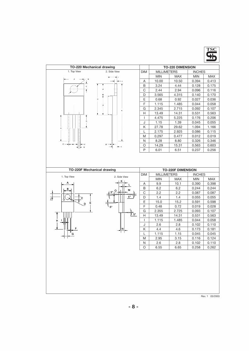
TO-220F DIMENSIONDIM MILLIMETERS INCHES
MIN MAX MIN MAXA 9.9 10.1 0.390 0.398B 6.2 6.2 0.244 0.244C 2.2 2.2 0.087 0.087D 1.4 1.4 0.055 0.055E 15.0 15.2 0.591 0.598F 0.48 0.72 0.019 0.028G 2.355 2.725 0.093 0.107H 13.49 14.31 0.531 0.563I 1.115 1.485 0.044 0.058J 2.6 2.8 0.102 0.110K 4.4 4.6 0.173 0.181L 1.115 1.15 0.045 0.045M 2.95 3.15 0.116 0.124N 2.6 2.8 0.102 0.110O 6.55 6.65 0.258 0.262
TO-220 DIMENSIONDIM MILLIMETERS INCHES
MIN MAX MIN MAXA 10.00 10.50 0.394 0.413B 3.24 4.44 0.128 0.175C 2.44 2.94 0.096 0.116D 3.565 4.315 0.140 0.170E 0.68 0.92 0.027 0.036F 1.115 1.485 0.044 0.058G 2.345 2.715 0.092 0.107H 13.49 14.31 0.531 0.563I 4.475 5.225 0.176 0.206J 1.15 1.39 0.045 0.055K 27.78 29.62 1.094 1.166L 2.175 2.925 0.086 0.115M 0.297 0.477 0.012 0.019N 8.28 8.80 0.326 0.346O 14.29 15.31 0.563 0.603P 6.01 6.51 0.237 0.256
TO-220 Mechanical drawing
TO-220F Mechanical drawing
1. Top View 2. Side View
1. Top View 2. Side View