Embed Size (px)
Citation preview

AN ALL-IMPLANTED CCD/CMOS PROCESS
DeWitt Ong*
ABSTRACT
A process has been developed that combines double po lys i l i con ,sur face type, n-channel CCD's wi th s i l i c o n gate CMOS c i r c u i t s on the same subs t r a te . The process is a l l ion-implanted ( inc lud ing the get ter s tep ) , and requires only one more masking step than a f u l l high voltage CMOS f low. Two CCD s h i f t reg is ters wi th in terna l CMOS peripheral c i r c u i t s , and a CMOS op-amp have been designed and characterized to demonstrate the design f l e x i b i l i t y afforded by the a v a i l a b i l i t y of both p and n channel t r ans i s to r s .
I . Advantages of CCD/CMOS
CMOS has several c i r c u i t performance advantages over NMOS that outweigh i t s addi t ional processing complexity. In d i g i t a l c i r c u i t s , CMOS has lower s t a t i c power, higher speed, and higher dr ive capab i l i t y ; whi le in l inear c i r c u i t s , i t has higher gain per stage, and wider input and output voltage swing. This paper describes a process that combines the superior performance of CMOS with double po l ys i l i con surface type n-channel CCD's. The process makes i t possible to have CCD wi th high speed CMOS clock dr ivers and peripheral c i r c u i t s . A l t e r n a t i v e l y , i t makes possible a d i g i t a l CMOS chip wi th CCD's as c i r c u i t funct ions.
I I . Device Cross-Section
A cross section of the resu l tan t s t ructure is shown in f i g . 1. The n-channel CCD is located in the P-tub reg ion, as is commonly done wi th n-channel t rans is to rs in CMOS. This contrasts wi th processes which s t a r t wi th an on-going CCD/NMOS f low, and locate the p-channel t rans is to rs in an N-tub. 1 The P-tub method, i t turns out , has several useful c i r c u i t design advantages, as w i l l be shown l a te r .
N-DOPED N-DOPED 1ST POLY T E O S + P-DOPED
Fig. 1 - Cross section of the CCD/CMOS s t ruc tu re .
*Motorola Phoenix Corporate Research and Development Center
291.
The CCD/CMOS process is f u l l y compatible wi th the 5 urn s i l i c o n gate Planox { loca l i zed oxidat ion of s i l i c o n ) CMOS f low. In f a c t , a l l process s p e c i f i cations are ident ica l except where obviously d i f f e r e n t , e . g . , second gate ox ide/poly . S i m i l a r i t i e s v i s i b l e in f i g . 1 are the f i e l d implants under the f i e l d oxide, and the so ca l led "double f lavor " poly , i . e . p-doped poly over p-channel t rans is to rs and n-doped poly over n-channel t r ans i s t o r s . Double f l avor poly reduces the magnitude of threshold vol tages; however, a metal strap is necessary fo r connecting the two poly types.
The CCD uses double poly to permit two phase operat ion. The f i r s t and second gate oxide thicknesses are 9.Q0A and 32QQA respect ive ly . The P^tub doping concentrat ion is 5 x 1 0 1 5 / c m 3 . An approximately 2 to 1 r a t i o in surface po ten t ia ls is obtained when +15V wi th respect to CCD substrate (P-tub) is applied to both electrodes. The 15 vo l ts are div ided in to 0 to +10V clock voltages and a -5V CCD substrate reverse bias.
While f i g . 1 shows the n-channel t r ans i s to r and CCD to be in the same P-tub, in general that i s not necessary. For example, the NMOS t rans is to rs of a CMOS clock d r iver c i r c u i t can be in a P^tub separate from that of the CCD i t d r ives . And by providing a negative bias to the CCD P-tub, the usual pos i t i ve t rans la t ion of a l l c locking wave form is conveniently obtained. A second benef i t of the separate P-tub concept is that the NMOS t rans is to rs now operate wi th less substrate b ias , g iv ing lower th res hold drops across such c i r c u i t s as the ubiquitous output source fo l lower .
I I I . Process
The masking sequence is given in Table I below:
Table I - Masking Sequence fo r CCD/CMOS
Substrate adjust (opposite of P-tub) Act ive area p - f i e l d n - f i e l d Tap (opt iona l ) 1st poly 2nd poly p+ source/drain n+ source/drain Preohmic Metal Passivation
Total number of masks: 1 1 + 1 opt ional
The basic masking sequence uses one more step (the 2nd poly) than the f u l l 18V high voltage CMOS f low.
There are s i gn i f i can t departures from the conventional s i l i c o n gate CMOS process, a l l slanted towards keeping the t o t a l number of masking steps down. The usual procedure is to s t a r t wi th a blanket phosphorus implant f o r substrate adjust . This is then fol lowed by a heavier boron implant to create the P-tub regions.
For the CCD/CMOS process, i t was decided to exclude the substrate adjust implant from the P-tub region in an attempt to increase i t s minor i ty
2 9 2 .

c a r r i e r l i f e t i m e . Th is was accompl ished w i t h o u t an e x t r a mask by means o f a n i t r i d e / o x i d e sequence i d e n t i c a l to the Planox p rocess . A n i t r i d e p a t t e r n p r o t e c t s the P-tub du r i ng subs t ra te a d j u s t imp lan t and the subsequent 10,0008 ox ide g rowth . The n i t r i d e i s then s t r i p p e d , l e a v i n g a t h i n l a y e r i n the ox ide f o r the boron to pene t ra te and form the t u b .
A second depar tu re from the convent iona l s i l i c o n gate CMOS i s i n the doping o f the f i r s t p o l y . I f the doping takes p lace a f t e r both po ly are p a t t e r n e d , the over lap reg ion between the two po ly would not get doped. So a f t e r the f i r s t po ly d e p o s i t i o n , a 2 x lO 'Vcnf 100 KeV phosphorus imp lan t i s per fo rmed, produc ing a sheet r es i s t ance o f IK f i / sq . a f t e r anneal
see F ig 2 ) . L a t e r , du r i ng the s o u r c e / d r a i n i m p l a n t , the exposed f i r s t po ly over the n-channel i s doped t o 35^ / sq . and po ly over p-channel i s doped to 107^ /sq . This process sequence a lso saves a masking s t e p .
The f i r s t gate ox ide i s grown a t 1050°C, w i t h dry 0 2 /6% HC1. When the second gate ox ide repeated the same cyc le w i t h a longer 0 2 /HC l t ime f o r the t h i c k e r o x i d e , severe " b l i s t e r i n g " o f the unde r l y i ng po ly 1 occu rs . A combinat ion wet 0 2 f o l l o w e d by dry O2 /HCI w i t h a d r y i ng t ime i n between e l i m i n a t e d the problem.
Device parameters averaged over severa l l o t s are presented i n Table I I .
Table I I - Average CCD/CMOS Parameters 1 1 1 1
1 pi vcm 3 a ) ^smzMiM^^mttzm
PHOS 2x1 ( W e m ' 100 KeV
D s u b s t r a t e I P-tub N A
tOX i
t o x 2
Vtn P o 1 y 1
V T N ^ 2
v tp poïy 1
n+ p.s
n+ po ly 1 n+ po ly 2 p+ p s
p+ po ly 1 tap p s
n+ V B
p+ V B
f i e l d V T over P-tub
I V . Ge t te r
Ps Ps
PS
6.5 x 5.2 x 1 0 1 5 / c m 3 • 9108 31808 0.62V 1.86V b) •
-0.60V 13 a/square 35 ft/square 42 ft/square 54 Q/square 107 SVsquare 84 ^ /square c ) 26V 24V 24V
Y77777\ YT7Z\
I I I I I I PHOS 7 n 1 0 1 s / c m 2
105 KeV
I Ki t , 3511
F i g , 1 - Implant sequence f o r double po ly CCD s t r u c t u r e .
The CCD/CMOS process i s a l l i on - imp lan ted f o r b e t t e r c o n t r o l and r e p r o d u c i b i l i t y . I t a l so min imizes the number o f h igh temperature s teps . Th is c a r r i e s over i n t o g e t t e r i n g as w e l l . Damage g e t t e r i n g 3 i s accomp l i s h e d by i m p l a n t i n g argon a t 100 Kev and a dose o f 3 x 1 0 1 5 / c m t o the back o f the wa fe r . Th is g e t t e r i s done as the very f i r s t s tep i n p r o c e s s i n g , and again j u s t a f t e r P-tub d r i v e - i n . Th is c o n t r a s t s w i t h the phosphorus g e t t e r i n g commonly used f o r NMOS, which i s g e n e r a l l y done as the l a s t h igh temperature step (s ince i t i s competing w i t h the h e a v i l y doped s o u r c e / d r a i n reg ions f o r the m e t a l l i c i m p u r i t i e s . ) As a r e s u l t , capac i t ance - t ime (C-T) response t imes i n the 60 t o 140 sec. range have been ob ta ined when a f i r s t gate ox ide c a p a c i t o r i s pulsed from -7.0V to
tlMl T ^ s ^ p r e s e n t s an average m i n o r i t y c a r r i e r l i f e t i m e o f 18 u s . " A d d i t i o n a l l y , i t was found t h a t the e l e c t r o n c a r r i e r l i f e t i m e i n s i d e the
2 9 3 ,

P-tub correlates well with the hole l i fet ime outside of i t . This would indicate that the minority carr ier l i fet ime is afunction of the start ing material and the processing i t sees, and that the P-tub doping is not heavy enough ,to create a difference.
On actual CCD sh i f t registers, chip delays of 1.35 seconds have been measured at room temperature. In addit ion, good uniformity of < ± 15% (see f i g . 3) in generation rate across a 64-bit sh i f t register has also been obtained. The good uniformity is at t r ibuted, for the most par t , to incorporation of HC1 during gate oxidation. Fig. 3 is obtained using the integration mode of operation 6 where the clock is stopped for a re lat ive ly long integration time before rapidly shi f t ing out. The individual output pulse then corresponds to the generation rate in one b i t posit ion.
Fig. 3 - Output from a 64 b i t sh i f t register after 600 ms of integration time, out of a possible maximum of 1.35 seconds, showing uniformity better than 15%.
V. Device Measurements
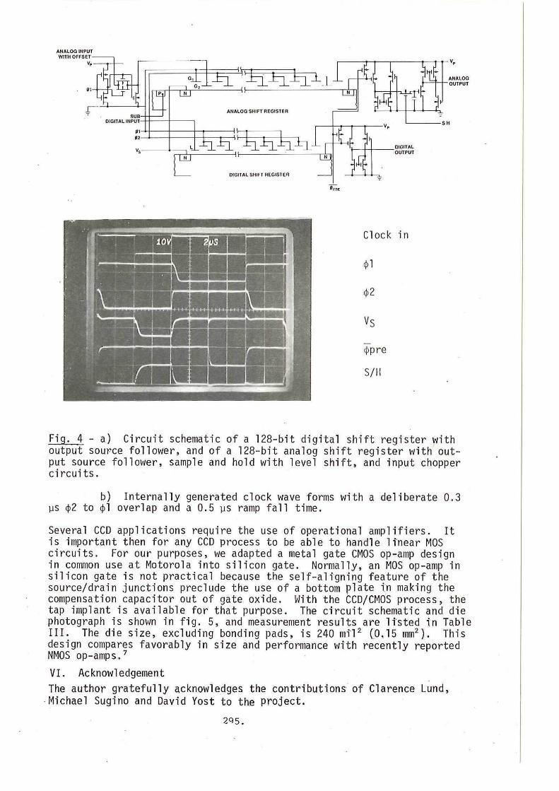
Several lots using two mask sets have been processed over a period of time. Among the c i rcu i t functions are two 128-bit sh i f t registers (see f i g . 4a). One is designed for d ig i ta l signals and has a 22 um b i t length and 10 um channel width. I t has an n-channel transistor source follower c i r cu i t with a current source for a load. The other is designed for analog inputs and has a 28 ym b i t length and a wider channel width of 100 urn for better signal to noise ra t io . I t has, in addition to the same output source follower c i r cu i t , an output sample and hold c i r cu i t with level sh i f t and an input chopping c i r cu i t . Note the design f l e x i b i l i t y afforded by the ava i lab i l i t y of both n and p channel transistors. Both registers have been operated with an internal CMOS clock driver (see f i g . 4b) at a typical transfer ineff ic iency, e of 1 x 10"3 at 25.6 KHz. Better devices with e <1.5 x 10~" have also been measured. A 550 mV output swingis available on the d ig i ta l register versus 6V on the analog
range i f f Y o m V ï o ^ / ^ ^ 1 n p U t V O l t a g e
2 9 4 .
ANALOG INPUT WITH OFFSET
Fig. 4 - a) C i r cu i t schematic of a 128-bit d i g i t a l s h i f t reg is te r wi th output source fo l lower , and of a 128-bi t analog s h i f t reg is te r wi th output source fo l lower , sample and hold wi th level s h i f t , and input chopper c i r c u i t s .
b) In te rna l l y generated clock wave forms wi th a del iberate 0.3 ps <f>2 to <J>i overlap and a 0.5 ps ramp f a l l t ime.
Several CCD appl icat ions require the use of operational amp l i f i e r s . I t is important then for any CCD process to be able to handle l inear MOS c i r c u i t s . For our purposes, we adapted a metal gate CMOS op-amp design in common use at Motorola in to s i l i c o n gate. Normally, an MOS op-amp in s i l i c o n gate is not p rac t ica l because the se l f - a l i gn ing feature of the source/drain junct ions preclude the use of a bottom plate in making the compensation capacitor out of gate oxide. With the CCD/CMOS process, the tap implant is avai lab le for that purpose. The c i r c u i t schematic and die photograph is shown in f i g . 5, and measurement resu l ts are l i s t e d in Table I I I . The die s i ze , excluding bonding pads, is 240 m i l 2 (.0,15 mm2). This design compares favorably in size and performance wi th recent ly reported NMOS op-amps. 7
VI . Acknowledgement
The author g ra te fu l l y acknowledges the cont r ibu t ions of Clarence Lund, Michael Sugino and David Yost to the p ro jec t .
2 9 5 .
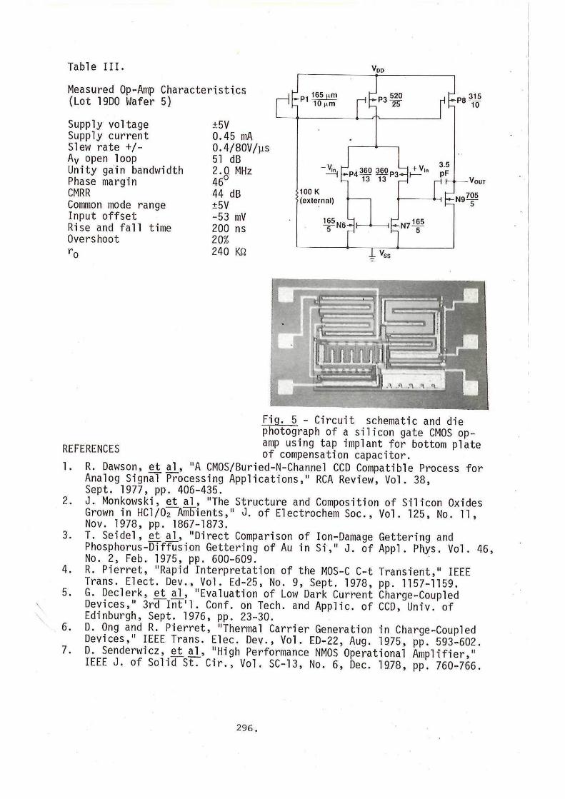
Table I I I .
Measured Op-Amp Character is t ics (Lot 19D0 Wafer 5)
Supply voltage Supply current Slew rate + / -A v open loop Unity gain bandwidth Phase margin CMRR Common mode range Input o f f se t Rise and f a l l time Overshoot
+5V 0.45 mA 0.4/80V/us 51 dB 2.0 MHz 46* 44 dB ±5V -53 mV 200 ns 20% 240 Kfi
^ f p 4 3 6 0 360 • ™ 13 13
100 K (external)
3.5
P F
N 9
- V O U T
705
Ty. ss
REFERENCES
1
5 - C i r cu i t schematic and die photograph of a s i l i con gate CMOS op-amp using tap implant fo r bottom plate of compensation capacitor.
"A CMOS/Buried-N-Channel CCD Compatible Process RCA Review, Vol . 38,
fo r R. Dawson, ej; al_ Analog Signal Processing App l ica t ions, Sept. 1977, pp. 406-435. J . Monkowski, et a]_, "The Structure and Composition of S i l i con Oxides Grown in HCl/0 2 Ambients," J. of Electrochem S o c , Vol. 125, No. 1 1 , Nov. 1978, pp. 1867-1873. T. Se ide l , et aj_, "Direct Comparison of Ion-Damage Gettering and Phosphorus-Diffusion Gettering of Au in S i , " J . o f Appl. Phys. Vol . 46, No. 2, Feb. 1975, pp. 600-609. R. P ie r re t , "Rapid In te rpre ta t ion of the MOS-C C-t Transient ," IEEE Trans. Elect . Dev., Vol . Ed-25, No. 9, Sept. 1978, pp. 1157-1159. G. Declerk, et al_, "Evaluation of Low Dark Current Charge-Coupled Devices," 3rd I n t ' l . Conf. on Tech. and Appl ic . of CCD, Univ. of Edinburgh, Sept. 1976, pp. 23-30. D. Ong and R. P ie r re t , "Thermal Carr ier Generation in Charge-Coupled Devices," IEEE Trans. Elec. Dev., Vol . ED-22, Aug. 1975, pp. 593-602. D. Senderwicz, e t al_s "High Performance NMOS Operational Amp l i f i e r , " IEEE J . of Sol id St. C i r . , Vol . SC-13, No. 6, Dec. 1978, pp. 760-766.
2 9 6 .