Embed Size (px)
Citation preview

AN EXPERIMENTAL INVESTIGATION OF AN ON-CHIP INTERCONNECT FABRIC
USING A MULTIPROCESSOR SYSTEM-ON-CHIP ARCHITECTURE
by
PRIYA BANGAL
KENNETH G. RICKS, COMMITTEE CHAIR
DAVID J. JACKSON KEITH A. WOODBURY
A THESIS
Submitted in partial fulfillment of the requirements for the degree of Master of Science
in the Department of Electrical and Computer Engineering in the Graduate School of
The University of Alabama
TUSCALOOSA, ALABAMA
2011

Copyright Priya Bangal 2011 ALL RIGHTS RESERVED

ii
ABSTRACT
Recent advances in technology have made it possible to integrate systems with CPUs,
memory units, buses, specialized logic, other digital functions and their interconnections on a
single chip, giving rise to the concept of system-on-chip (SoC) architectures. In order to keep up
with the incoming data rates of modern applications and to handle concurrent real-world events
in real-time, multiprocessor SoC implementations have become necessary. As more processors
and peripherals are being integrated on a single chip, providing an efficient and a functionally
optimum interconnection has become a major design challenge. The traditional shared-bus-based
approach is quite popular in SoC architectures as it is simple, well-understood and easy to
implement. However, its scalability is limited, since the bus invariably becomes a bottleneck as
more processors are added. Switch-based networks can overcome this bottleneck while providing
true concurrency and task-level parallelism, resulting in a higher throughput. However, switch-
based networks are complex and consume considerable amounts of logic resources on a chip,
thus increasing the cost. Hence, the choice of switch-based networks over a bus-based
architecture is an important design consideration in SoC architectures. This choice hinges on the
trade-off between design simplicity and low cost vs. high communication bandwidth. This
research investigates the logic resource utilization of a switch-based on-chip interconnect to
analyze its scalability for multiprocessor systems. It also experimentally demonstrates the true
concurrency provided by the interconnect, investigates the arbitration mechanism used, and
suggests the use of a real-time operating system (RTOS) as a more effective way of managing
on-chip interconnections.

iii
DEDICATION
To my late father, who made me want to be an engineer; and to my mother, who made it
possible.

iv
LIST OF ABBREVIATIONS AND SYMBOLS
AHB Advanced High-performance Bus
ALU Arithmetic Logic Unit
AMBA Advanced Microcontroller Bus Architecture
APB Advanced Peripheral Bus
API Application Programming Interface
ARM Advanced RISC Machines
AS Active Serial
ASB Advanced System Bus
ASIC Application-Specific Integrated Circuit
BFT Butterfly Fat-Tree
CLASS Chip Level Arbitration and Switching System
CPLD Complex Programmable Logic Device
CPU Central Processing Unit
DAC Digital-to-Analog Converter
DMA Direct Memory Access
EDS Embedded Design Suite
FPGA Field Programmable Gate Array
FSL Fast Simplex Links
GUI Graphical User Interface
HDL Hardware Description Language

v
I/O Input/Output
IBM International Business Machines
IC Integrated Circuit
IDE Integrated Development Environment
IP Intellectual Property
ISA Instruction Set Architecture
JTAG Joint Test Action Group
LE Logic Element
LED Light Emitting Diode
LMB Local Memory Bus
MIMD Multiple Instruction, Multiple Data
MIPS Million Instructions Per Second
MISD Multiple Instruction, Single Data
MM Memory-Mapped
MMU Memory Management Unit
NRE Non-Recurring Engineering
PCB Printed Circuit Board
PLB Processor Local Bus
PLL Phase Locked Loop
PTF Peripheral Template File
RAM Random Access Memory
RISC Reduced Instruction Set Computer
RTL Register Transfer Level
vi
RTOS Real-Time Operating System
SBT Software Build Tools
SD Secure Digital
SDRAM Synchronous Dynamic RAM
SIMD Single Instruction, Multiple Data
SISD Single Instruction, Single Data
SoC System-On-Chip
SOPC System-On-Programmable-Chip
SRAM Static RAM
TDMA Time Division Multiple Access
UART Universal Asynchronous Receiver/Transmitter
USB Universal Serial Bus
VGA Video Graphics Array
VHDL Very-High-Speed Integrated Circuits HDL

vii
ACKNOWLEDGEMENTS
As I draw my graduate studies to a closure, it would be imprudent of me to fail to
acknowledge those I worked with on my way to becoming a Master of Science. The process has
been tedious and challenging, but also very enjoyable.
I am heavily indebted to my advisor Dr. Kenneth Ricks, whom I most closely worked
with during this research. Dr. Ricks inspired and convinced me to blaze the Multiprocessor
System-on-chip trail at the University of Alabama. He instilled in me the confidence that what I
was doing was worthwhile and that I could do it with the minimal available groundwork. From
him, I learned to use experimental approaches for solving computer engineering problems. Dr.
Ricks always had a remarkable insight into the arbitration aspect of the on-chip interconnect,
which was one of the areas of focus in this research. He remained closely involved in my work
so that our research meetings were always very constructive. His cheerful nature and sense of
humor made him fun to work with (even though I was at the receiving end of most of his
practical jokes!). His expertise in the areas of Computer Architecture and Embedded Systems
Design has been instrumental in shaping my graduate career. Thank you, Dr. Ricks, for being my
mentor.
I would also like to express my gratitude to Dr. Jeff Jackson and Dr. Keith Woodbury for
agreeing to be invaluable members of my thesis committee. Dr. Jackson provided resourceful
guidance throughout this research, especially for using the Quartus II and SOPC Builder tools.
He also helped me in understanding some key concepts in Digital Logic Design and in
interpreting SignalTap Logic Analyzer Waveforms. I am also grateful to my friends and fellow

viii
graduate students Smita Potdar, Scott Corley, Brooks Latta and Chris Hall for being available for
brainstorming, sharing information and also for being great friends. Thanks guys, for lending me
pencils, books, screwdrivers and other random stuff; for patiently listening to me whine about
temperamental instruments and software tools, and for walking over to Starbucks for coffee
when the walls of HO 220 seemed to close in on me. My friends Meghna Dilip, Manjusha
Vaidya and Vineeth Dharmapalan helped in proof reading and formatting this thesis. I am
thankful for their support and friendship.
I am profoundly grateful to the wonderful staff at the Office of Institutional Research and
Assessment and to Dr. Susan Burkett, Professor of Electrical and Computer Engineering, with
whom I worked as a graduate assistant at the University of Alabama. Both jobs were very
enjoyable, fruitful and great learning experiences that I shall always cherish. I must also
acknowledge Debbie, Moe and Leslie from the ECE office who have not only been very helpful,
but have always done so with a smile on their face. I remain indebted to my extended family and
friends who have been supportive of all my endeavors. My mother has ensured that I had
everything I needed to get through graduate school and my little sister has always looked up to
me and motivated me to be a better person and a better engineer. I am thankful for them and also
for Ranjan Dharmapalan, my companion in graduate school and best friend in the world, who
has been there to love my flawed heart.
Last but not the least, I am grateful to everyone I have met and known at the University
of Alabama and in the lovely town of Tuscaloosa, Alabama. Everyone who made my stay here
an enriching experience, who taught me to say “Roll Tide” and to love all things Crimson, who
made me feel at home when I was across the globe from my home in India. Yea Alabama, you’ll
always be Sweet Home to me!

ix
CONTENTS
ABSTRACT .................................................................................................................................... II
DEDICATION .............................................................................................................................. III
LIST OF ABBREVIATIONS AND SYMBOLS ......................................................................... IV
ACKNOWLEDGEMENTS ......................................................................................................... VII
CONTENTS .................................................................................................................................. IX
LIST OF TABLES ....................................................................................................................... XII
LIST OF FIGURES ................................................................................................................... XIII
CHAPTER 1 BASIC INTERCONNECTION ARCHITECTURES .............................................. 1
1.1 Flynn’s Taxonomy ........................................................................................................... 2
1.2 Shared Memory vs. Distributed Memory ......................................................................... 4
1.3 Interconnection Networks ................................................................................................ 5
1.4 Multiprocessor System-on-Chip and Interconnection Networks ................................... 10
1.5 Thesis Motivation and Goal ........................................................................................... 11
CHAPTER 2 TYPICAL SOC ARCHITECTURES ..................................................................... 13
2.1 SoC Processor Cores ...................................................................................................... 13
2.2 SOPC Design vs. Traditional Design Considerations .................................................... 15
2.3 SoC Interconnections ..................................................................................................... 18
2.3.1 Shared-Medium Networks ............................................................................................. 18
2.3.2 Hybrid Networks ............................................................................................................ 19
2.3.3 Switch-based Networks .................................................................................................. 20
2.4 Related Work.................................................................................................................. 22

x
CHAPTER 3 SYSTEM DETAILS ............................................................................................... 24
3.1 Development Environment ............................................................................................ 24
3.1.1 The Altera DE2 Board.................................................................................................... 24
3.1.2 Altera Quartus II and SOPC Builder .............................................................................. 26
3.1.3 Nios II Processor ............................................................................................................ 29
3.1.4 Nios II Integrated Development Environment ............................................................... 30
3.1.5 SignalTap II Embedded Logic Analyzer ....................................................................... 30
3.2 The Implementation Process .......................................................................................... 32
3.3 Creating Multiprocessor Systems using the Nios II Processor ...................................... 33
3.3.1 Independent Multiprocessor Systems ............................................................................ 33
3.3.2 Dependent Multiprocessor Systems ............................................................................... 34
3.4 Adapting Multiprocessor System Designs to the DE2 Platform .................................... 35
3.4.1 Using the On-Board SDRAM ........................................................................................ 36
3.4.2 Tuning the PLL .............................................................................................................. 37
CHAPTER 4 THE SYSTEM INTERCONNECT FABRIC: IMPLEMENTATION AND LOGIC UTILIZATION ................................................................................................................ 39
4.1 Description and Fundamentals of Implementation ........................................................ 39
4.2 Logic Resource Utilization............................................................................................. 42
4.2.1 Experiment 1: Multiple CPUs, One Slave ..................................................................... 42
4.2.2 Experiment 2: One CPU, Multiple Slaves ..................................................................... 48
4.2.3 Experiment 3: Multiple CPUs, Multiple Slaves ............................................................. 53
4.3 Logic Utilization by the Fabric: A Comparison ............................................................. 57
4.4 Scalability in Comparison with a Traditional Shared-Bus ............................................. 59
CHAPTER 5 THE SYSTEM INTERCONNECT FABRIC: ARBITRATION ........................... 61
5.1 Multimaster Architecture and Slave-Side Arbitration ................................................... 61
5.2 Traditional Shared-Bus Architectures vs. Slave-Side Arbitration ................................. 63

xi
5.2.1 Traditional Shared-Bus Architectures ............................................................................ 63
5.2.2 Slave-Side Arbitration .................................................................................................... 66
5.3 Demonstrating True Concurrency Using the Partial Crossbar Fabric............................ 69
5.4 Throughput Improvement .............................................................................................. 75
5.5 Fairness-Based Arbitration Shares ................................................................................. 81
CHAPTER 6 CONCLUSIONS .................................................................................................... 89
6.1 Summary ........................................................................................................................ 89
6.2 Future Work ................................................................................................................... 91
REFERENCES ............................................................................................................................. 93
APPENDIX A ............................................................................................................................... 96
A.1 Hardware and Software Requirements .......................................................................... 96
A.2 To Begin ......................................................................................................................... 96
A.3 Creating a SOPC System with two CPUs ...................................................................... 97
A.3 Creating Software for the multiprocessor systems ....................................................... 103
A.4 Tuning the PLL ............................................................................................................ 104
A.5 Building Independent Multiprocessor Systems............................................................ 104
APPENDIX B ............................................................................................................................. 106
B.1 VHDL declarations for cpu_data_master_arbitrator .................................................... 106
B.2 VHDL declarations for cpu_instruction_master_arbitrator ......................................... 109
B.3 VHDL declarations for jtag_debug_module_arbitrator ............................................... 111
B.4 VHDL declarations for onchip_memory_arbitrator ..................................................... 113
APPENDIX C ............................................................................................................................. 116
C.1 Nios II assembly language programs executing on two CPUs to drive two LED banks independently.................................................................................................................... 116
C.2 Nios II assembly language programs executing on two CPUs to access two different memory banks independently ...................................................................................... 117

xii
LIST OF TABLES
1. Features of Commercial Soft Processor Cores for FPGAs ....................................................... 15
2. Comparison of SOPC, ASIC and Fixed-processor Design Parameters .................................... 16
3. Logic Resource Utilization: Multiple CPUs, One Slave .......................................................... 46
4. Logic Resource Utilization: One CPU, Multiple Slaves .......................................................... 51
5. Logic Resource Utilization: Multiple CPUs, Multiple Slaves .................................................. 55
6. Comparison between Estimated and Actual Logic Utilization in Experiment 3 ...................... 57

xiii
LIST OF FIGURES
1. A General Block Diagram Showing Flynn’s Taxonomy ............................................................ 3
2. Shared Memory vs. Distributed Memory ................................................................................... 4
3. Network Topologies.................................................................................................................... 5
4. A Typical Shared Bus Architecture ............................................................................................ 7
5. A Crossbar Network ................................................................................................................... 9
6. AMBA-Based Design of an ARM Microcontroller SoC .......................................................... 19
7. The Altera DE2 Board .............................................................................................................. 25
8. SOPC Builder Graphical Interface ............................................................................................ 28
9. SignalTap II Editor ................................................................................................................... 31
10. Flowchart Describing the SoC Implementation ...................................................................... 32
11. Independent Multiprocessor System ....................................................................................... 33
12. Dependent Multiprocessor System with a Shared Resource .................................................. 34
13. Partitioning of the SDRAM Memory Map for two processors ............................................... 37
14. System Interconnect Fabric: Example System ....................................................................... 40
15. Experimental Setup for a System with Multiple CPUs and One Slave ................................. 43
16. SOPC Builder System with Multiple CPUs, One Slave ......................................................... 44
17. Graphical Representation of the Increase in Logic Utilization with Increase in Number of CPUs. ........................................................................................................................................ 47
18. Experimental Setup for a System with One CPU, Multiple Slaves ........................................ 49
19. Graphical Representation of the Increase in Logic Utilization with Increase in Number of Slaves. ....................................................................................................................................... 52
20. Experimental Setup for a System with Multiple CPU-Slave Pairs ......................................... 54

xiv
21. Graphical Representation of the Increase in Logic Utilization as More CPU-Slave Pairs Are Added. .................................................................................................................................... 56
22. Comparison of Logic Utilization by the System Interconnect Fabric for Three Different Experiments .................................................................................................................................. 58
23. A Traditional Shared Bus Architecture ................................................................................... 63
24. Experimental Setup to Demonstrate the Behavior of a Traditional Bus-Based System ......... 64
25. Master request and Slave granted Signals Demonstrating Bus-like Behavior ...................... 65
26. Slave-Side Arbitration ............................................................................................................ 67
27. Multimaster Connections on the System Interconnect Fabric ................................................ 68
28. Arbiter Logic on the System Interconnect Fabric ................................................................... 69
29. SOPC Builder System with Independent I/O Slaves .............................................................. 70
30. Concurrent Communications with I/O Slaves ........................................................................ 71
31. SOPC Builder System with Independent Memory Slaves ...................................................... 72
32. Concurrent Communications with Memory Slaves ................................................................ 74
33. Experimental Setup with One CPU and One Slave to Investigate Throughput ..................... 76
34. Response of the System with One CPU and One Slave for Throughput Investigation .......... 77
35. Response of a Bus-Based System for Throughput Investigation............................................ 78
36. Experimental Setup with Two CPUs and Two Slaves to Investigate Throughput ................. 79
37. Response of the System with Two Masters and Two Independent Slaves for Throughput Investigation .................................................................................................................................. 80
38. Arbitration Share Settings in the SOPC Builder Connections Matrix .................................... 81
39. SOPC Builder System Used to Examine the Behavior of Arbitration Shares ........................ 83
40. Output Waveforms with 1:1 Arbitration Shares ..................................................................... 84
41. Output Waveform of a Six CPU System Performing Continuous Reads from the Same Memory Slave ............................................................................................................................... 87
A.1 Nios II Processor MegaWizard .............................................................................................. 99
A.2 Shared Resource Connections in SOPC Builder ................................................................. 102

1
CHAPTER 1
BASIC INTERCONNECTION ARCHITECTURES
Since the beginning of computing, scientists and engineers have endeavored to make
machines solve problems faster and better. Traditional designs for a computer system involve
one Central Processing Unit (CPU) – a uniprocessor. However, there are inherent limitations on
the extent to which the performance of a uniprocessor system can be improved. Heat dissipation
and electromagnetic interference will always limit the transistor density on a chip. There are also
economic constraints when the cost of making a processor incrementally faster and more
efficient exceeds the price that anyone is willing to pay. In the light of these limitations, the most
feasible way of improving performance is to distribute the computational load among multiple
processors (Null & Lobur, 2006). For this reason, parallel processing and multiprocessor
architectures have become increasingly popular in the world of computer engineering.
However, it is important to note that multiprocessor architectures may not be suitable for
all applications. Multiprocessing parallelism adds to the cost as it requires considerably larger
amounts of hardware resources. Process synchronization and other aspects of process
administration add to the overhead of the system. In addition, every algorithm will have a certain
number of tasks that must be executed sequentially. Additional processors can do nothing but
wait until this serial processing is complete, which limits the speedup achievable through a
multiprocessor implementation. The greater the sequential processing requirement, the less cost
effective it is to implement a multiprocessor architecture. Therefore, a thorough analysis of the

2
price/performance ratio is necessary before porting an application to a multiprocessing parallel
architecture. Implemented wisely, multiprocessor architectures yield a significant speedup,
higher throughput, better fault tolerance and a higher cost-benefit ratio for suitable applications
(Null & Lobur, 2006).
As multiprocessors and other alternative computer architectures gained popularity over
traditional uniprocessor systems, there was a need to categorize these architectures in order to
study them. Over the years, several attempts have been made to find a satisfactory way to
classify computer architectures. Although none of them are perfect, a widely accepted taxonomy
is Flynn’s taxonomy.
1.1 Flynn’s Taxonomy
In 1966, Michael Flynn proposed a system to categorize computer architectures, which is
widely accepted today as Flynn’s taxonomy (Flynn, 1966). Figure 1 shows a diagrammatic
representation of Flynn’s taxonomy. The four categories as defined by Flynn are based upon the
number of concurrent instruction and data streams available in the architecture:
• Single Instruction, Single Data Stream: A SISD machine is a sequential computer
which implements no parallelism in either the instruction or data streams.
Traditional uniprocessor systems are SISD machines
• Single Instruction, Multiple Data Streams: SIMD machines, which have a single
point of control, execute the same instruction simultaneously on multiple data
values. E.g. Array and vector processors.
• Multiple Instruction, Single Data Stream: MISD machines have multiple
instruction streams operating on the same data stream. This is a rather uncommon

3
architecture and is generally used for fault-tolerance. In fact, it is a shortcoming of
Flynn’s taxonomy that there seem to be very few, if any, applications for MISD
machines.
• Multiple Instruction, Multiple Data Streams: MIMD machines, which have
multiple control points, have independent instruction and data streams.
Multiprocessors and most current parallel systems are MIMD machines (Flynn M.
J., 1966).
Figure 1. A General Block Diagram Showing Flynn’s Taxonomy (Null & Lobur, 2006)
Although Flynn’s taxonomy provides a basic characterization of computer architectures,
it falls short in several areas. One major problem with the taxonomy is that each category is very
broad, consisting of several different architectures. For example, no distinction is made within
the MIMD category depending on how the processors are connected or how they access

4
memory. There have been several attempts to redefine the MIMD category. Suggested changes
include subdividing MIMD to differentiate between systems that share memory and those that do
not, and categorizing systems according to the kind of interconnection network used (Null &
Lobur, 2006). This research uses a multiprocessor architecture that falls under the MIMD
category of Flynn’s taxonomy. Therefore, it is important to understand the various subdivisions
and architectures possible in the MIMD category. Sections 1.2 and 1.3 discuss some of the
subdivisions of the MIMD category.
1.2 Shared Memory vs. Distributed Memory
Shared memory systems are those in which all processors have access to a global
memory and communicate through shared variables. Distributed memory systems are systems in
which processors do not share memory but each processor owns a portion of memory. However,
communication between processors is essential for synchronized processing and data sharing.
Since there is no shared memory, processors must communicate with each other by passing
messages explicitly through an interconnection network (Null & Lobur, 2006). Figure 2 is a
block diagram showing the difference between shared memory systems and distributed memory
systems.
Figure 2. Shared Memory vs. Distributed Memory (Null & Lobur, 2006)

5
The way in which the processors are interconnected, called the network topology, is a
major factor determining the bandwidth and overhead cost of message passing in a system.
Hence, network designs attempt to minimize both, the required overhead and distances over
which messages must travel. Various interconnection network topologies have been proposed to
support architectural scalability and provide efficient performance for parallel programs
(Duncan, 1990).
1.3 Interconnection Networks
Interconnection networks define the manner in which the processors, memory and other
peripherals in a system are connected to each other. Figure 3 shows some popular network
topologies that are discussed below.
Figure 3. Network Topologies (Null & Lobur, 2006)

6
Completely connected networks are those in which all the network components are
directly connected to all other components by dedicated connection links. Although these
networks provide excellent connectivity between all nodes, their major advantage is that they are
very expensive to build and require a considerable amount of hardware resources. As new
components are added, the number of connections, c, increases quadratically according to the
equation:
(1)
where: n is the number of nodes in the system.
Hence, completely connected networks become increasingly difficult to build and manage and
do not scale well for a system with a large number of processors (Null & Lobur, 2006).
Star connected networks have a central hub through which all processors in the system
communicate with each other. Although the hub provides excellent connectivity to all nodes in a
system, it can be a potential bottleneck as the number of nodes increases. Linear arrays or linear
networks allow any node in the network to communicate with its two neighboring nodes directly,
but any other communication must go through multiple nodes to arrive at its destination (Null &
Lobur, 2006). The ring is just a variation of a linear array in which the two end nodes are directly
connected. The communication links in the ring topology may be unidirectional or bi-directional.
Linear and ring topologies also do not scale well for large systems and are most appropriate for a
small number of processors executing algorithms not dominated by data sharing.
A two-dimensional mesh network links each node to its four immediate neighbors.
Wraparound connections (like those in a ring) or additional diagonal links may be provided. Tree
networks arrange the nodes in a hierarchical structure that branches out from a single node,
called the root. Tree structures have a potential for communication bottlenecks forming closer to

7
the roots. A possible augmentation is to add additional connection pathways connecting nodes at
the same hierarchical level (Duncan, 1990). Hypercube networks are multidimensional
extensions of mesh networks. In an n-dimensional hypercube, each processor is connected to n
other processors. So, the total number of nodes, N, in an n-dimensional hypercube is:
N = 2n (2)
These networks also get unwieldy for larger dimensions. Also, the loss of a single node may
require substantial changes to the remaining network topology (Duncan, 1990).
Two more types of widely used interconnection networks are: Bus-based networks and
switch-based networks. Bus-based networks are the simplest and the most popular. All the
components in a bus-based system are connected to a single communication link, called the bus.
The bus is shared by multiple components in the system to communicate with one another.
Figure 4 shows a typical bus-based network with multiple processors, memory and Input/Output
(I/O) components.
Figure 4. A Typical Shared Bus Architecture

8
The main advantage of a bus-based network is that new components can be easily added
to the network without redefining the connection scheme. Buses are also cost effective because a
single communication link is shared by multiple components. However, it is necessary to define
a scheme or a protocol so that the bus can be reserved by the device that wishes to use it for
communication. Without such a scheme, multiple devices can assume control of the bus at the
same time, resulting in communication contention and collisions. This is avoided by introducing
bus masters and bus slaves in the system. A device that can initiate and control transfers across
the bus is defined as the bus master. A device that responds to bus transfer requests, but never
initiates a transfer on its own is called a slave. A processor must be able to initiate bus requests
for accessing memory and I/O, therefore a processor is always a bus master. Memory always
responds to read or write requests but never initiates a transfer, so memory is usually a slave.
Communication across the bus is simple if there is only one processor i.e. only one bus
master in the system. In a system with multiple processors, a scheme is necessary to decide
which master will use the bus next. This is called bus arbitration and involves specialized
hardware called the arbiter. When multiple masters request to access the bus at the same time,
the arbiter chooses one master depending on the arbitration scheme and grants the bus to that
master. The rest of the requesting masters have to wait until the chosen master completes its
transfer. Clearly, the most significant disadvantage of a bus-based system is that, as multiple
processors request the bus simultaneously, the wait-time for each processor increases. This
results in a communication bottleneck and a lower throughput. Bus-based networks are thus most
effective when the number of processors in the system is moderate.
Switch-based networks use switches to dynamically alter routing across the network.
Crossbar networks use multiple switches that are either open or closed, so that any component in

9
the system can be connected to any other component by closing the switch (making a
connection) between them. Networks consisting of crossbar switches are fully connected because
any component can be connected with any other component and simultaneous connections
between different processor-memory pairs are possible. Crossbar networks are typically used in
high performance computing applications because they are very flexible, provide very high
throughput and a high degree of concurrency (Null & Lobur, 2006). Figure 5 shows a crossbar
switch network.
Figure 5. A Crossbar Network (Null & Lobur, 2006)
Crossbars are typically implemented with large multiplexers. The hardware resource
utilization grows exponentially as more components are added to the system, making it costly
and difficult to manage. In order to optimize the hardware utilization, a partial crossbar network
may be used. In these systems, individual processors may require to communicate with only a
subset of the system components. A partial crossbar network provides connectivity between only

10
those components which need to communicate with each other. The components which never
communicate with each other are not connected, thus saving hardware resources.
1.4 Multiprocessor System-on-Chip and Interconnection Networks
System-on-a-Chip (SoC) is the idea of integrating all components of a computer system
into a single integrated circuit (IC). Recent advances in technology have made it possible to
integrate systems with one or multiple CPUs, memory units, buses, specialized logic, other
digital functions and their interconnections on a single chip. An SoC implementation has several
advantages over a traditional implementation. Integrating several components/functions into one
chip eliminates the need to physically move data from one chip to another, thereby achieving
higher speeds. Many modern applications such as cellular phones, telecommunication and
networking, digital televisions and video gaming require chip speeds that are unattainable with
separate ICs. Circuit operations that occur on a single IC require much less power than a similar
circuit implemented on a printed circuit board with discrete components. SoC implementation
greatly reduces the size and power consumption of the system, while also generally reducing
manufacturing costs (Jerraya & Wolf, 2005).
However, in some cases, SoC implementations of uniprocessor systems may not provide
enough performance for computation-intensive applications. Multicore processors were
introduced as the first step towards importing a multiprocessor computing environment to a
single chip. Interconnection of the multiple cores became an important design consideration.
Although multicore processors are not SoCs, their commercial availability has paved the way for
multiprocessor SoC implementations. Multiprocessor SoC implementations are needed to keep
up with the incoming data rates of modern embedded applications and to handle concurrent real-

11
world events in real-time. These increasing levels of on-chip integration mean that more
processors and other functional units need to be interconnected. It is a major design challenge to
provide an efficient and a functionally optimum SoC interconnection that will satisfy the needs
for modular and robust design, under the constraints posed by the logic resources available on a
single chip. SoC interconnection networks have therefore garnered interest as a separate area of
research in computer engineering in recent years.
1.5 Thesis Motivation and Goal
SoC networks are very similar to interconnection networks discussed in Section 1.3,
where multiprocessor systems have processors as individual chips. The traditional shared-bus-
based approach discussed in Section 1.3 is quite popular in SoC architectures as well, because it
is simple, well-understood and easy to implement. However, its scalability is seriously limited,
since the bus invariably becomes a bottleneck as more processors are added. Another critical
limitation of shared-bus architectures is their energy inefficiency. In these architectures, every
data transfer is a broadcast, which must reach each possible receiver thus requiring a large
energy cost. Future SoC systems will contain tens to hundreds of units that generate information
to be transferred. For such systems, a bus-based architecture would become a critical
performance and power bottleneck (Jerraya & Wolf, 2005).
Switch-based networks, like the crossbar network discussed earlier, overcome the
scalability problems of the shared-bus architecture. Unlike shared-bus architectures, the total
communication bandwidth in a switching network increases as the number of nodes in the
system increases. Switches do not perform information processing, but only provide a
programmable connection between components or in other words, set up a communication path

12
that can be changed over time (Jerraya & Wolf, 2005). Unlike shared-bus architectures,
switching networks provide true concurrency and task-level parallelism, resulting in a higher
throughput. Switching networks are typically implemented using large multiplexers. Multiplexer
input is selected depending on which switch must be closed. These multiplexers consume
considerable amounts of logic resources on a chip. Since most current SoC systems are
implemented on Field Programmable Gate Arrays (FPGAs), larger systems need FPGAs with
more logic elements which are increasingly expensive.
Hence, the choice of switch-based networks over a bus-based architecture is an important
design consideration in SoC architectures. This choice essentially hinges on the trade-off
between design simplicity and low cost vs. true parallelism, high throughput, high
communication bandwidth, and additional complexity.
The goal of this thesis is to observe, analyze and document the logic utilization of a
switch-based SoC interconnection as the number of components in the system is changed. This
will help designers in performing a better cost-benefit analysis while choosing a switch-based
interconnection over a traditional shared-bus approach. This thesis also demonstrates true
parallelism of switched-based SoC networks as opposed to time-sharing on a traditional bus-
based architecture and compares the throughput of the two.

13
CHAPTER 2
TYPICAL SOC ARCHITECTURES
This chapter provides a brief overview of typical SoC systems and introduces the
System-On-Programmable-Chip (SOPC) based design approach to building SoC systems. It also
discusses a few typical SoC interconnections and introduces the system interconnect fabric by
Altera, which is the main on-chip interconnect that has been under consideration for this
research. Lastly, it discusses the related work in the field of SoC interconnections analysis and
evaluation and defines the objectives of this thesis.
2.1 SoC Processor Cores
A new technology has emerged in SoC designs, enabling designers to utilize a large
FPGA that contains both memory and logic elements along with an intellectual property (IP)
processor core to implement custom hardware for SoC applications. This new approach has been
termed as System-On-a-Programmable-Chip (SOPC) (Hamblen, Hall, & Furman, 2008).
Processor cores are classified as either “hard” or “soft” depending on their
flexibility/configurability. Hard processor cores are less configurable but tend to have higher
performance characteristics as compared to soft cores.
Hard processor cores use a fully implemented embedded processor core (in dedicated
silicon) in addition to the FPGA’s normal logic elements. Hard processor cores added to an

14
FPGA creates a hybrid approach, offering performance characteristics that fall somewhere
between a traditional Application-Specific Integrated Circuit (ASIC) and an FPGA. They are
available from several manufacturers with a number of different processor types. For example,
Altera Corporation, a leading manufacturer of reprogrammable logic devices, offers an
Advanced RISC Machines (ARM) processor core embedded in its APEX 20KE family of
FPGAs that is marketed as an ExcaliburTM device. Xilinx Inc., another leading manufacturer of
logic devices, makes a family of FPGAs called Virtex II pro that includes up to four PowerPC
processor cores on-chip. Cypress Semiconductor also offers a Programmable-System-on-Chip
(PSoCTM) that is formed on an M8C processor core with configurable logic blocks designed to
implement the peripheral interfaces, which include analog-to-digital converters, timers, counters
and UARTs (Hamblen, Hall, & Furman, 2008).
Soft processor cores, sometimes referred to as synthesizable cores, use the existing
programmable logic elements from the FPGA to implement the processor logic. Soft cores
consist of a synthesizable hardware model, typically in the form of a netlist or a Hardware
Description Language (HDL) code that is extremely flexible and easy to optimize (Duncan,
1990). Altera’s Nios II and Xilinx’s MicroBlaze are examples of soft core processors. As evident
from Table 1, soft processor cores can be very feature-rich and flexible, allowing the designer to
specify the memory width, the Arithmetic Logic Unit (ALU) functionality, number and types of
peripherals and memory address space parameters at compile time. However, this flexibility
comes with a trade-off. Soft cores have slower clock rates and more power usage than an
equivalent hard processor core. Considering the current prices of large FPGAs, the addition of a
soft processor core costs very little based on the logic elements it requires. The remaining logic

15
elements on the FPGA can be used to build application-specific system hardware (Hamblen,
Hall, & Furman, 2008).
Table 1. Features of Commercial Soft Processor Cores for FPGAs (Xilinx, Inc., 2008) (Altera Corporation, 2009)
Feature
Nios II 9.1 MicroBlaze v9.0
Datapath
32 bits 32 bits
Pipeline Stages
1, 5 or 6 3 or 5
Frequency
Up to 200 MHz Up to 200MHz
Register File 32 general purpose and 32 control registers
32 general purpose and 32 special purpose registers
Instruction Word
32 bits 32 bits
Instruction Cache
Optional Optional
Hardware Multiply and Divide
Optional Optional
2.2 SOPC Design vs. Traditional Design Considerations
Traditional embedded computer systems may be implemented using ASICs or discrete
components such as processors and memory devices. ASICs use semi-custom or full-custom IC
technology, where the lower levels of gate arrays are already built on the IC and the designer can
connect these gate arrays to achieve the desired implementation. ASICs usually require a long
design time and involve a high non-recurring engineering (NRE) cost, depending on the degree
of custom IC technology used. Fixed-processor systems are traditional discrete component IC
systems that use off-the-shelf processors such as Intel Atom, International Business Machines
(IBM) PowerPC, ARM and others. SOPC design is implemented on FPGAs, in which all levels
of logic already exist on the chip. These layers implement a programmable circuit specified by
16
the designer. Although ASICs and fixed-processor systems offer higher performance, they have
large developmental costs and turnaround times. SOPC design has advantages and disadvantages
to both of these alternatives, as demonstrated in Table 2. The advantages of an SOPC design are
flexibility and a short development cycle. The trade-offs include lower performance, higher unit
costs in production and relatively high power consumption.
Table 2. Comparison of SOPC, ASIC and Fixed-processor Design Parameters (Hamblen, Hall, & Furman, 2008)
Feature
SOPC ASIC Fixed-Processor
S/W Flexibility
Good Good Good
H/W Flexibility
Good Poor Poor
Reconfigurability
Good Poor Poor
Development Time/Cost
Good Poor Good
Peripheral Equipment Costs
Good Good Poor
Performance
Moderate Good Good
Production Cost
Moderate Good Good
Power Efficiency
Poor Good Good
There are several benefits of having a flexible hardware infrastructure that is offered by
SOPC designs. Features and specifications of a design may need modification based on
marketing demands or change in a protocol, specification or other surrounding technology (e.g.,
USB 2.0 is introduced, demand drops for cell phones without Bluetooth etc.). In traditional
design modalities, these changes can dramatically affect the ASIC design, processor selection
and/or printed circuit board (PCB) design. Since the hardware architecture is often settled upon

17
early in the design cycle, making changes to the hardware design later in the cycle is more
difficult and more expensive, typically resulting in delay of a product’s release. SOPC designs,
on the other hand, are easy to modify and reconfigure.
With flexible and reconfigurable logic, a single PCB can be designed and used in
multiple product lines as well as in multiple generations/versions of a single product. Using
reconfigurable logic at the heart of a design allows it to be reprogrammed to implement a wide
range of systems and designs. Extending the life of a board design even by a generation results in
significant savings and can largely offset the increased per-unit expense of reconfigurable
devices.
The SOPC design approach is ideal for research projects as well. SOPC boards can be
used and reused to support an extremely wide range of student projects at a very low cost. ASIC
development times are too long and mask setup fees are too high to be considered for prototypes
generally used in research projects. Using discrete components requires additional hardware and
perhaps a new PCB for each application. Given the complexity of today’s multilayer surface
mount PCBs, it is highly unlikely that researchers will have enough time and funds to develop a
new PCB for each design project. Hence the reconfigurability and reusability of SOPC-based
designs make them ideal for research projects and prototypes.
This research uses the Nios II soft processor core from Altera and adopts the SOPC
design approach for building multiprocessor SoC systems.
18
2.3 SoC Interconnections
For the traditional approach as well as for the SOPC design approach to SoC systems, the
major challenge that designers must overcome is to provide functionally correct and reliable
operation of the interacting components. On-chip physical interconnections present a limiting
factor for performance and energy consumption. Hence, extensive research has been done on
SoC interconnects and various architectures have been proposed and implemented over the
years. As discussed in Chapter 1, Section 1.5, SoC interconnections are closely related to
interconnection networks in multiprocessor systems where the processors are discrete
components. Similar to traditional multiprocessor systems, SoC nodes are physically close, with
high link reliability; and the bandwidth and latency constraints are stringent in order to support
effective parallelization. On-chip interconnections can be classified in a similar way and their
evolution follows a path similar to that of multiprocessor interconnection architectures (Benini &
De Micheli, 2002).
2.3.1 Shared-Medium Networks
Most current SoC interconnection architectures use shared-medium networks. These are
the simplest interconnect structures in which the transmission medium is a bus that is shared by
all the processors and peripherals in the system. The bus is usually passive and does not generate
any control or data messages. Bus arbitration mechanisms are required when several processors
attempt to use the bus simultaneously. Arbitration is generally performed in a centralized fashion
by a bus arbiter module.
The Advanced Microcontroller Bus Architecture (AMBA), a bus standard designed for
the ARM processor family, is an example of a shared-bus SoC architecture. It is fairly simple

19
and widely popular today. AMBA covers two distinct buses: The Advanced System Bus (ASB)
and the Advanced Peripheral Bus (APB). The ASB is the main system bus that allows high-
bandwidth communication between the masters and the most significant slave devices, such as
the external memory controller. The APB is a minimalist, low-bandwidth peripheral I/O bus that
emphasizes a low-gate-count implementation for each peripheral. There is no activity on the
APB, except when an I/O access takes place. Thus, the high-bandwidth bus activity between the
processor and on-chip memory is decoupled from the peripheral bus (Flynn D. , 1997). Figure 6
shows an AMBA-based design of an ARM microcontroller SoC.
Externalbus External
businterface
TIC(master)
Arbiter
ARM DMA
RAM Decoder
ASBB
ridg
eAPB
UART
Timer
PIO
RTC
Figure 6. AMBA-Based Design of an ARM Microcontroller SoC (Flynn D. , 1997)
This design encourages modularity and reusability by partitioning the high and low
bandwidth activities on two independent buses. This is also beneficial from an energy viewpoint.
Connection between the two different protocols is supported through the bus bridge.
2.3.2 Hybrid Networks
Hybrid networks are networks that support more than one communication protocol. Since
AMBA allows ‘clustering’ of high and low bandwidth computational units using different

20
protocols and provides inter-cluster communication links, it is also classified as a
‘heterogeneous’ or ‘hybrid’ architecture. The AMBA 2.0 standard which was released later,
introduced the Advanced High-performance Bus Protocol (AHB) which was an improvement
over the original ASB (Aldworth, 1999).
MicroBlaze, the soft processor core from Xilinx, also employs multiple bus protocols to
accommodate its various performance needs. Local Memory Bus (LMB) is used for a fast local
access memory. Xilinx Cache Link is a point-to-point interface for direct connection between
cache and external memory. Processor Local Bus (PLB46) is used for connecting multiple
peripherals directly to MicroBlaze. There are also up to 16 co-processor links called the Fast
Simplex Links (FSL) that can be used for hardware acceleration (Xilinx, Inc, 2010). Thus, a
typical MicroBlaze SoC system is also an example of a hybrid network.
2.3.3 Switch-based Networks
Although bus-based networks are widely popular, they have obvious problems such as
performance bottleneck and lower throughput as the number of processors in the system is
increased. The limitations of bus-based systems have already been discussed in Chapter 1,
Section 1.5. Switch-based networks overcome some of the problems of bus-based networks.
Freescale Semiconductor, another leading semiconductor manufacturer, employs an on-
chip switching interconnect called the Chip Level Arbitration and Switching System (CLASS) in
several of their devices (Freescale Semiconductor, 2009). CLASS is a non-blocking, full-fabric
crossbar switch that allows any master to access any slave in parallel to any other master-slave
couple access, as long as the two masters access two different slaves. CLASS is based upon well-
defined building blocks and uses a standard, well-defined, high-performance interface. CLASS

21
also implements a powerful arbitration scheme that includes four priority levels, automatic
priority upgrading, pseudo round-robin arbitration on each priority level, priority mapping,
priority masking and weighted arbitration (Goren & Netanel, 2006).
Altera Corporation provides a high-bandwidth interconnect structure, called the system
interconnect fabric, for connecting various components in SoC systems. The system
interconnect fabric is a partial crossbar structure that provides concurrent paths between master-
slave pairs. The system interconnect fabric is based on the Avalon® Interface Specifications and
all components in the system must adhere to these specifications. For each component in the
system, the fabric manages transfers with every connected component. Master and slave
interfaces can contain different signals and the system interconnect fabric handles any
adaptations necessary between them. In the path between masters and slaves, the fabric might
introduce registers for timing synchronization, finite state machines for event sequencing, or
nothing at all depending on the services required by the specific interfaces (Altera Corporation,
2008).
Since the system interconnect fabric is a partial crossbar, it utilizes less logic than a full
crossbar. But since it is generated using the SOPC approach, it still provides high flexibility,
reconfigurability, and high throughput. Altera provides a tool, called the SOPC Builder, whose
primary function is to generate the system interconnect fabric based on the component
connections specified by the designer. Altera’s system interconnect fabric is the primary switch-
based SoC interconnect considered for study in this thesis.

22
2.4 Related Work
In embedded systems design, the need to customize the system architecture for a specific
application or domain cannot be overemphasized. With the availability of several different SoC
interconnection architectures, the choice of an optimum interconnect for a certain design has
become more crucial to designers than ever before. This makes it necessary for designers to be
aware of and to evaluate the trade-offs involved in selecting one architecture over the other.
While it is generally known that different communication architectures may be better suited to
serve the needs of different applications, little work has been done on quantitatively
characterizing and comparing their performance and expenditure.
An evaluation methodology has been proposed to study the performance metrics of
various interconnection architectures for different classes of communication traffic (Lahiri,
Raghunathan, & Dey, 2001). This methodology was tested for specific topologies such as
shared-bus, hierarchical bus, two-level time division multiple access (TDMA) and ring. Another
evaluation methodology proposed by the researchers at the University of British Columbia was
tested on more complex topologies such as the Butterfly Fat-Tree (BFT) and the mesh (Pande,
Grecu, Jones, Ivanov, & Saleh, 2004). While this work has been very useful in defining an
approach for evaluation of SoC interconnects in general, none of them have been tested on a
dynamic topology such as a switch-based crossbar. It has also not considered the flexibility and
reconfigurability offered by an SOPC approach while evaluating the trade-offs.
Research has been done to evaluate and compare the power requirements and
performance of crossbars and buses in SoC designs, using custom-designed crossbars and buses
(Zhang & Irwin, 1999). This work gives a clear comparison of bus vs. crossbar power and
performance, but the experimental results cannot be used for real-world design considerations as

23
they were implemented on custom components rather than on commercially available
interconnects.
Researchers at the University of Bologna in Italy have performed a scalability analysis on
three commercially popular shared-bus protocols: STBus by STMicroelectronics and AMBA
AXI and AMBA AHB by ARM. They observed that STBus and AMBA AXI exhibit better
scalability as compared to AMBA AHB, in terms of benchmark execution times and bus usage
efficiency (Ruggiero, Angiolini, Poletti, & Bertozzi, 2004).
For comparison, the research presented in this thesis performs a scalability analysis on
Altera’s system interconnect fabric. The system interconnect fabric is autogenerated by the
synthesis tool after the design components are specified by the user. This research investigates
the implementation and functional details of the autogenerated system interconnection fabric to
analyze its scalability for multiprocessor systems. The objectives of this research are as follows:
1. To understand the structural details and implementation of the system
interconnect fabric.
2. To experimentally determine the on-chip logic resource utilization by the fabric as
the number of masters and slaves in the system vary.
3. To understand and experimentally investigate the arbitration mechanism in the
system interconnect fabric.
4. To experimentally demonstrate true concurrency provided by the partial crossbar
architecture as opposed to a time multiplexed bus-based system.
24
CHAPTER 3
SYSTEM DETAILS
This chapter describes in detail the hardware and software development platform used in
this research. It provides details about the design tools used and also enlists the features of the
Nios II processor, which is the primary soft processor core used in this research. Finally, it
describes the steps involved and challenges faced in the system implementation, some of which
are unique to this research.
3.1 Development Environment
3.1.1 The Altera DE2 Board
Figure 7 shows the DE2 Development and Education Board from Altera that is used in
this project as the hardware platform. The DE2 board features a state-of-the-art Altera Cyclone®
II 2C35 FPGA device in a 672-pin package. The Cyclone® II 2C35 FPGA has 33,216 Logic
Elements (LEs) and 483,840 total random access memory (RAM) bits. All important
components on the board are connected to pins of the FPGA, allowing the user to control all
aspects of the board’s operation. It is easy to instantiate Altera’s Nios II processor and use
interface standards such as RS-232, PS/2 and Joint Test Action Group (JTAG) Universal
Asynchronous Receiver/Transmitter (UART) (Altera Corporation, 2006). The following
hardware is provided on the DE2 board:

25
• Altera Cyclone® II 2C35 FPGA device
• Altera Serial Configuration device – EPCS16
Figure 7. The Altera DE2 Board (Altera Corporation, 2006)
• Universal Serial Bus (USB) Blaster for programming and user Application Programming
Interface (API) control
• Support for JTAG and Active Serial (AS) programming modes
• 512-Kbyte Static Random Access Memory (SRAM)
• 8-Mbyte Synchronous Dynamic Random Access Memory (SDRAM)
• 4-Mbyte Flash memory (1 Mbyte on some boards)
• Secure Digital (SD) Card socket
• 4 pushbutton switches
26
• 18 toggle switches
• 18 red user Light Emitting Diodes (LEDs)
• 9 green user LEDs
• 50-MHz oscillator and 27-MHz oscillator for clock sources
• 4-bit CD-quality audio Codec with line-in, line-out, and microphone-in jacks
• Video Graphics Array (VGA) Digital-to-Analog Converter (DAC) (10-bit high-speed
triple DACs) with VGA-out connector
• TV Decoder and TV-in connector
• 10/100 Ethernet Controller with a connector
• USB Host/Slave Controller with USB type A and type B connectors
• RS-232 transceiver and 9-pin connector
• PS/2 mouse/keyboard connector
• IrDA transceiver
• Two 40-pin Expansion Headers with diode protection
3.1.2 Altera Quartus II and SOPC Builder
The Altera Quartus II is a comprehensive, multiplatform FPGA and Complex
Programmable Logic Device (CPLD) design tool. It integrates full featured tools for all stages of
design flow into one efficient interface. An exhaustive suite of synthesis, optimization,
simulation, verification, timing analysis, power management and device programming tools is
provided in a single, unified design environment. Quartus II adapts to allow for flexible design
flow methodologies. It has an advanced Graphical User Interface (GUI) and also a command-line

27
scripting interface that allows maximum efficiency and automation of common processes (Altera
Corporation, 2008). Quartus II Version 8.0 is used for this research.
SOPC Builder, an exclusive Quartus II tool, is a powerful system development tool for
defining and generating a complete SOPC in much less time than using traditional, manual
integration methods. SOPC Builder is included as part of the Quartus II software. It automates
the task of integrating hardware components such as processors, memories, standard peripherals
and user-defined peripherals. Using SOPC Builder, the designer can specify the system
components in a GUI and SOPC Builder generates the interconnect logic automatically. In
addition to its role as a system generation tool, SOPC Builder provides features to ease writing
software and to accelerate system simulation (Altera Corporation, 2008). Figure 8 shows a
snapshot of the SOPC Builder graphical interface.

28
Figure 8. SOPC Builder Graphical Interface
There is a peripheral template file (PTF) associated with each SOPC Builder project. The
user-specified options, settings and parameters in the SOPC Builder GUI are used to generate the
PTF file, which defines the role, structure and functionality of each component in the system.
The PTF file is passed on to the HDL generator during the Quartus II compilation, which creates
the actual register transfer level (RTL) description of the system using the Very-high-speed
integrated circuits HDL (VHDL). The SOPC Builder tool is used extensively in this research to
develop multiprocessor SoC systems.

29
3.1.3 Nios II Processor
The Nios® II processor is a popular soft processor core from Altera. It is available as a
standard component in the SOPC Builder Tool within Altera Quartus II. It is a general-purpose,
32-bit reduced instruction set computer (RISC) processor core, with salient features as follows:
• Full 32-bit instruction set, data path, and address space
• 32 general-purpose registers
• 32 interrupt sources
• External interrupt controller interface for more interrupt sources
• Single-instruction 32-bit × 32-bit multiply and divide producing a 32-bit result
• Dedicated instructions for computing 64-bit and 128-bit products of multiplication
• Floating-point instructions for single-precision floating-point operations
• Single-instruction barrel shifter
• Access to a variety of on-chip peripherals, and interfaces to off-chip memories and
peripherals
• Hardware-assisted debug module enabling processor start, stop, step, and trace
under control of the Nios II software development tools
• Optional memory management unit (MMU) to support operating systems that
require MMUs
• Optional memory protection unit (MPU)
• Software development environment based on the GNU C/C++ tool chain: Nios II
Integrated Development Environment (IDE) and the Nios II Software Build Tools (SBT)
for Eclipse

30
• Integration with Altera's SignalTap® II Embedded Logic Analyzer, enabling real-time
analysis of instructions and data along with other signals in the FPGA design
• Instruction set architecture (ISA) compatible across all Nios II processor systems
• Performance up to 250 Dhrystone million instructions per second (MIPS)
Since the Nios II is a soft core, it is highly configurable. Designers can add or remove
features on a system-by-system basis to meet performance or price goals. A typical Nios II
processor system consists of a Nios II processor core, a set of on-chip peripherals, on-chip
memory, and interfaces to off-chip memory all implemented on a single Altera FPGA device. All
Nios II processor systems use a consistent instruction set and programming model (Altera
Corporation, 2008).
3.1.4 Nios II Integrated Development Environment
The Nios II Integrated Development Environment (IDE) is a graphical software
development tool for the Nios II processor. All software development tasks, including editing,
building, and debugging programs can be accomplished using the Nios II IDE. The IDE allows
users to create single-threaded programs as well as complex applications based on a real-time
operating system (RTOS) and middleware libraries available from Altera and third-party
vendors. Nios II IDE Version 8.0 is used during this research to create and build user
applications and download them to the target hardware.
3.1.5 SignalTap II Embedded Logic Analyzer
The SignalTap® II Logic Analyzer is a scalable and easy-to-use logic analyzer included
with the Quartus II software package. This logic analyzer helps debug the FPGA design by

31
probing the state of the internal signals in the design without the use of external equipment.
Trigger-conditions can be custom-defined to provide greater accuracy and better ability to isolate
problems. All captured signal data is conveniently stored in device memory. Since the most
required on-chip resource for the logic analyzer is the memory, SignalTap II has a built-in
resource estimator that calculates amount of memory that each logic analyzer instance uses. The
resource estimator reports the ratio of total RAM usage in the design to the total amount of RAM
available. The resource estimator also provides a warning if there is potential for a “no-fit”
(Altera Corporation, 2009). Figure 9 shows the user interface of the SignalTap II Logic
Analyzer.
Figure 9. SignalTap II Editor

32
3.2 The Implementation Process
The SoC is created using the SOPC Builder and Quartus II software tools. The steps
involved in the implementation process are presented in the form of a flowchart in Figure 10.
Figure 10. Flowchart Describing the SoC Implementation

33
3.3 Creating Multiprocessor Systems using the Nios II Processor
The Nios II IDE, the Quartus Programmer and the Nios II configuration manager,
collectively known as the Nios II Embedded Design Suite (EDS), allow for creating
multiprocessor systems in which the processors are independent, as well as those in which
processors share resources.
3.3.1 Independent Multiprocessor Systems
In independent multiprocessor systems, the processors are completely independent and
do not communicate with the each other and are thus incapable of interfering with each other’s
operation. Hence, such systems are typically less complicated and pose fewer challenges. Figure
11 shows a block diagram of an independent multiprocessor system.
Figure 11. Independent Multiprocessor System (Altera Corporation, 2007)

34
3.3.2 Dependent Multiprocessor Systems
Dependent multiprocessor systems are those in which the processors share resources. In
these systems, the design challenge is to have processors operate efficiently together and to
minimize contention for shared resources. To prevent conflicts between processors, a hardware
mutex core is included in the SOPC Builder component library. The hardware mutex core allows
different processors to claim ownership of a shared resource for a period of time. This temporary
ownership of a resource by a processor prevents the shared resource from being accessed by
another processor at the same time. The most common type of shared resource in multiprocessor
systems is memory. In general, with the exception of the mutex core, Nios II EDS does not
support sharing non-memory peripherals among multiple processors (Altera Corporation, 2007).
Figure 12 shows a block diagram of a dependent multiprocessor system with a shared memory
component.
Figure 12. Dependent Multiprocessor System with a Shared Resource (Altera Corporation, 2007)

35
3.4 Adapting Multiprocessor System Designs to the DE2 Platform
This research uses independent as well as shared memory multiprocessor systems for an
experimental investigation of the system interconnection fabric. Altera offers a detailed tutorial
on building shared memory multiprocessor systems (Altera Corporation, 2007). The tutorial
relies extensively on design examples included in the Nios II EDS and is designed to be used
with the development board included in the ‘Nios II Development Kit’. Research described in
this thesis uses the DE2 development board instead and as a result, the design examples in the
Nios II EDS could not be used. So, for this research, a new implementation process had to be
created specifically for the DE2 development board. First, a uniprocessor system was created
and tested using the DE2 board and the design process used in the textbook by Hamblen et al.
(Hamblen, Hall, & Furman, 2008). From this basic uniprocessor system, multiprocessor systems
were created using the Altera tutorial (Altera Corporation, 2007) as a guideline. This involved
the following major steps:
1. Replacing SRAM in the uniprocessor system with SDRAM: The DE2 board has 512
Kbytes of SRAM. This memory is sufficient for uniprocessor systems, but may not be
sufficient for executing software on multiple processors. For multiprocessor systems,
SDRAM, which is 8 Mbytes, must be used. Section 3.4.1 describes how the on-board
SDRAM is used as program memory for multiprocessor systems.
2. Tuning the Phase Locked Loop (PLL) for SDRAM: The SDRAM and the Nios II
processor operate on different clock edges (Hamblen, Hall, & Furman, 2008). The
SDRAM needs a clock signal that is phase-shifted by 180 degrees. An inverter can do
this, but the phase-shift needs to be further adjusted slightly to correct for the internal
FPGA delays. To create a phase-shifted clock signal for the SDRAM, a PLL component

36
is included in the design. Section 3.4.2 provides details about the phase-shift adjustment
of the PLL component.
3. Testing the SDRAM: After adding SDRAM and the PLL to the uniprocessor system, it is
tested using a sample application.
4. Adding multiple processors to the system: Multiple processors are then added to the
system, closely following the method described in the Altera tutorial (Altera Corporation,
2007).
5. Partitioning the SDRAM: The SDRAM must be partitioned to be used by multiple
processors. This is described in section 3.4.1.
6. Writing software to be executed on multiple processors: A sample application is provided
by Altera to test multiprocessor systems.
Appendix A provides step-by-step instructions for creating a multiprocessor SoC using the DE2
board.
3.4.1 Using the On-Board SDRAM
When creating multiprocessor systems, software for each processor must be located in its
own unique region of memory called the program memory. In the Nios II EDS, those regions are
allowed to reside in the same physical memory device. Nios II and SOPC Builder provide a
simple scheme of memory partitioning within this shared memory device. The partitioning
scheme uses the exception address for each processor, which is set in SOPC Builder, to
determine the region of memory from which each processor is allowed to execute its software
(Altera Corporation, 2007). In this research, 8 MBytes of on-board SDRAM is used as the

37
program memory. The 8 Mbytes is evenly divided among the processors in the system. The
memory partitions for a two-processor SoC are shown in Figure 13.
Figure 13. Partitioning of the SDRAM Memory Map for two processors (Altera Corporation, 2007)
3.4.2 Tuning the PLL
The SDRAM and the Nios II processor operate on different clock edges (Hamblen, Hall,
& Furman, 2008). To create a phase-shifted clock signal for the SDRAM, a PLL component is
implemented on the FPGA. The phase shift value for this PLL must be specified in the Quartus II

38
MegaWizard Plug-In Manager. This value is recommended as -54 deg (corresponding to -3 ns)
for Quartus II Version 7.1, but may differ slightly for later versions of the software. However, it
is noted to fall within 30 degrees of -54 degrees for most designs. This corresponds to a time
delay adjustment of up to 2 ns (Hamblen, Hall, & Furman, 2008). This research project uses
Quartus II Version 8.0 and designs with a PLL phase shift value of -54 degrees created errors on
this platform.
However, it was not clear whether this problem was related to the tuning of the PLL or to
the SDRAM component itself. To establish this, SRAM was temporarily set to be program
memory and the SDRAM was tested by implementing individual read and write transfers with it.
Interestingly, individual transfers to the SDRAM succeeded. Software could perform read and
write operations to the SDRAM, but the same software could not execute when the code was
located in the SDRAM. As described in the Quartus II Handbook, Section I: Off-chip Interface
Peripherals (Altera Corporation, 2009) this is a symptom of an untuned PLL.
Additional tuning of the PLL component was performed using a trial-and-error approach.
Finally, a PLL phase-shift value of -45 degrees (corresponding to -2.5 ns) resulted in successful
program downloads to the SDRAM.

39
CHAPTER 4
THE SYSTEM INTERCONNECT FABRIC: IMPLEMENTATION AND LOGIC
UTILIZATION
The system interconnect fabric for memory-mapped interfaces is a high-bandwidth
interconnect structure created by Altera Corporation. It is used for connecting components in
SoC designs that use the Avalon Memory-Mapped (Avalon-MM) interface. The system
interconnect fabric provides greater design flexibility and higher throughput than a typical time
multiplexed system bus (Altera Corporation, 2009). Altera also provides a system interconnect
fabric for streaming interfaces (Avalon-ST), which creates datapaths for unidirectional flow of
traffic among components. But since memory-mapped components are more versatile and more
widely used compared to streaming components, the system interconnect fabric for memory-
mapped interfaces is primarily considered for this study. This chapter describes the functions of
the system interconnect fabric for memory-mapped interfaces and the implementation of those
functions.
4.1 Description and Fundamentals of Implementation
The system interconnect fabric is an autogenerated interconnection structure. It is a
collection of synchronous logic and routing resources that connects Avalon-MM master and
slave components in a system. It guarantees that signals are routed correctly between masters and
slaves. The memory-mapped masters and slaves in the system must adhere to the Avalon

40
Interface Specifications (Altera Corporation, 2009). The SOPC Builder autogenerates the system
interconnect fabric to match the needs of the components in a system.
The system interconnect fabric implements a partial crossbar interconnect structure that
provides concurrent paths between masters and slaves. This is ideal for FPGA designs because
the SOPC Builder only generates the logic necessary to connect masters and slaves that
communicate with each other (Altera Corporation, 2008). Masters and slaves that never
communicate with each other need not be connected, thus saving a considerable amount of logic
resources. This provides the performance of a full crossbar fabric, with the flexibility of the
SOPC design approach. If the system design changes and new connections between masters and
slaves are needed, the system interconnect fabric can be regenerated automatically using the
SOPC Builder. Figure 14 shows a simplified diagram of the system interconnect fabric in an
example memory-mapped system with multiple masters.
Figure 14. System Interconnect Fabric: Example System (Altera Corporation, 2009)

41
As seen in Figure 14, the system interconnection fabric provides arbitration for shared
slaves on the slave side of the fabric. The slave-side arbitration and concurrent communication
paths significantly reduce the contention for resources that is inherent in a shared-bus
architecture. In this example system, the processor has exclusive access to the instruction
memory using a dedicated communication path, so there is never contention for this slave
resource, and rightfully so since this slave is dedicated to the processor. The SDRAM is shared
by the processor and the Direct Memory Access (DMA) Controller, so there is a slave-side
arbiter to control access to the SDRAM. Slave-side arbitration is further discussed in Chapter 5.
The system interconnect fabric supports components with multiple Avalon-MM
interfaces, such as the processor component shown in Figure 14. For each component interface,
the system interconnect fabric manages Avalon-MM transfers, interacting with signals on the
connected component. Master and slave interfaces can contain different signals and the system
interconnect fabric handles any adaptation necessary between them. In the path between master
and slaves, the system interconnect fabric might introduce registers for timing synchronization,
finite state machines for event sequencing, or nothing at all, depending on the services required
by the specific interfaces (Altera Corporation, 2009).
The system interconnect fabric performs the following functions:
• Address Decoding
• Datapath Multiplexing
• Wait State Insertion
• Pipelined Read Transfers
• Arbitration for Multimaster Systems
• Burst Adapters

42
• Handling Interrupts
• Reset Distribution
The behavior of these functions in a specific system largely depends on the design of the
components in the system and the user-defined settings in the SOPC Builder.
4.2 Logic Resource Utilization
The system interconnect fabric for Avalon-MM interfaces is a partial crossbar switch
fabric and is implemented using large multiplexers. As the number of components in a design
increases, the number and width of these multiplexers increases. Also, more interconnections are
needed to connect these components with one another. Therefore, the number of FGPA logic
elements required to implement the system interconnect fabric increases. Although this fabric
requires less logic resources than a full crossbar, it is not very lightweight. This section
investigates the logic footprint of the system interconnect fabric based on experimental
observations.
4.2.1 Experiment 1: Multiple CPUs, One Slave
This experiment observes the increase in the logic utilization of the system interconnect
fabric as more CPUs are added to the SOPC system. Figure 15 shows the block diagram of the
experimental setup used for this. The Nios II/e “economy” cores, which consume fewer than 700
logic elements, are used as the master CPUs in this experiment. On-chip RAM is used as the
slave. Since memory is separate from the LEs on the Cyclone II device, the on-chip memory
slaves are not synthesized using LEs and do not impact the logic element count of the design.
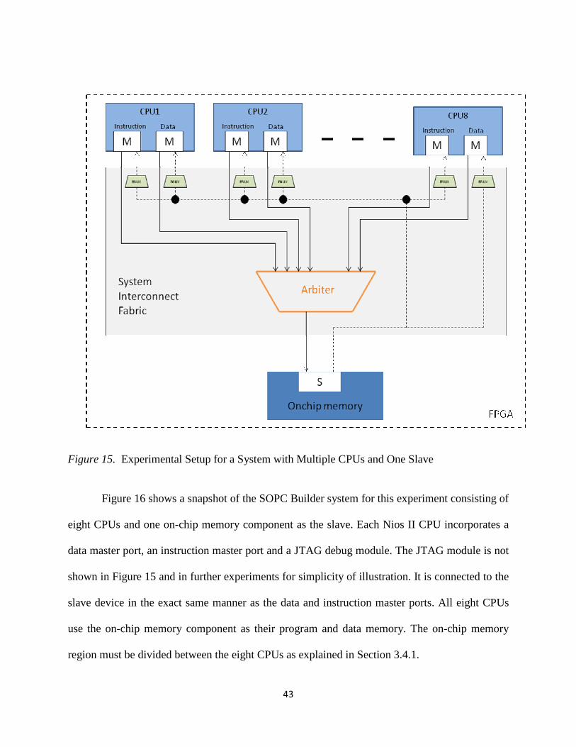
43
Figure 15. Experimental Setup for a System with Multiple CPUs and One Slave
Figure 16 shows a snapshot of the SOPC Builder system for this experiment consisting of
eight CPUs and one on-chip memory component as the slave. Each Nios II CPU incorporates a
data master port, an instruction master port and a JTAG debug module. The JTAG module is not
shown in Figure 15 and in further experiments for simplicity of illustration. It is connected to the
slave device in the exact same manner as the data and instruction master ports. All eight CPUs
use the on-chip memory component as their program and data memory. The on-chip memory
region must be divided between the eight CPUs as explained in Section 3.4.1.

44
Figure 16. SOPC Builder System with Multiple CPUs, One Slave
When the system is generated using the SOPC Builder, a PTF file is generated as
described in Section 3.1.2. The PTF file is passed on to the HDL generator during the Quartus II
compilation which creates the actual RTL description of the system. After the addition of each
Nios II/e CPU, the VHDL code for the system which is autogenerated by Quartus II, is examined
for changes. The VHDL code before the addition of the CPU is compared with the code after the
addition of the CPU and it is found that the following factors contribute to the increase in logic
utilization of the system interconnect fabric:
• With the addition of each CPU, its data and address buses are added to the system
interconnect fabric.

45
• There is datapath multiplexing logic associated with each master in the system. Since
each CPU has a data master port, an instruction master port, and a JTAG debug module,
there are separate multiplexers for each of these ports. Therefore, with the addition of one
CPU, three multiplexers are introduced into the system as part of the system interconnect
fabric. These multiplexers are shown in green in Figure 15. These multiplexers are also
referred to as “arbitrators” in the system VHDL file, since they arbitrate access to the
master.
• Slave-side arbitration is needed at the on-chip RAM as multiple masters are sharing it. As
the number of CPUs in the system increases, the width of this slave-side arbiter increases.
The slave-side multiplexer is shown in orange in Figure 15.
Appendix B lists the VHDL code for the description of components of the system
interconnect fabric associated with the addition of a new CPU. These components do not change
for different types of Nios II cores, namely Nios II/s “standard” core and Nios II/f “fast core”.
Hence, it can be safely assumed that the logic resource utilization of the fabric does not differ for
different types of Nios II CPU cores.
Table 3 summarizes total logic resource utilization by the SOPC system, as the number of
CPUs is increased incrementally from one to eight. Each additional CPU adds three additional
masters to the system (instruction port, data port, and debug module). The total number of LEs
used by the system is obtained using the Quartus II compilation report. The percentages in Table
3 are percentages of the total logic resources available on the FPGA, 33,216 (Altera Corporation,
2005).

46
Table 3. Logic Resource Utilization: Multiple CPUs, One Slave
It is observed that the total logic utilization increases by approximately 3% for every
master that is added to the system. ∆LE indicates the increase in the total number of LEs used
with the addition of each CPU. The NiosII/e CPU consumes from 600 to 700 LEs (Altera
Corporation, 2008). A worst-case number of 700 LEs is assumed in Table 3. The 700 LEs
assumed for each CPU include all three master ports. The logic utilization by the fabric is
calculated by subtracting the NiosII/e core logic consumption from the total logic consumption.
∆LEfabric_cpu indicates the increase in the number of LEs used by the fabric with the addition of
each CPU. Figure 17 is a graphical representation of the data from Table 3. It can be seen that
the increase in the total number of LEs used and the LEs used by the fabric is fairly linear as the
number of CPUs is increased.
Number of CPUs (Nios II/e
Cores) (N)
Total Number of LEs used
(LEtotal)
Increase in total
LEs used
(∆LE)
Percentage of LEs used
LEs used by Nios II/e
cores (LEcpu)
LEs used by Fabric (LEfabric)
Increase in LEs used by
fabric (∆LEfabric_cpu)
1 1539 5% 700 839 2 2596 1057 8% 1400 1196 357 3 3587 991 11% 2100 1487 291 4 4651 1064 14% 2800 1851 364 5 5609 958 17% 3500 2109 258 6 6607 998 20% 4200 2407 298 7 7598 991 23% 4900 2698 291 8 8618 1020 26% 5600 3018 320
Average 311

47
Figure 17. Graphical Representation of the Increase in Logic Utilization with Increase in Number of CPUs.
Based on the observations in this experiment, the following equation can be used to describe the
effect of adding CPUs to the SOPC system:
LEtotal = LEcpu(N) + [ LEfabric + N(∆ LEfabric_cpu)] (3)
where: LEcpu = Number of LEs per CPU (which is 700 for the Nios II/e core)
N = Number of CPUs
LEfabric = The baseline number of LEs required for the fabric (The value 839 from Table 3
represents this variable. This is the number of LEs required for the most basic fabric
interconnection between one CPU and one slave.)
∆ LEfabric_cpu = The average number of additional LEs required for the fabric for each added CPU
(This value is 311, from Table 3)

48
Equation (3) can be used to extrapolate the data from Table 3 and estimate the total logic
utilization of SOPC systems with more than eight CPUs.
4.2.2 Experiment 2: One CPU, Multiple Slaves
This experiment investigates the increase in logic utilization as more slaves are added to
the system. Similar to the previous experiment, one Nios II/e CPU is used and on-chip memory
components are used as slaves. As explained in Experiment 1, the on-chip memory slaves do not
consume LEs. The number of slaves is increased, in unitary increments, from one to eight and
the corresponding logic resource utilization of the system is noted. The change in LEs used is
attributed to the interconnect fabric since the CPU does not change and the slaves consume no
LEs. Figure 18 shows a block diagram of this experimental architecture. The JTAG debug
module, although present in the CPU, is not shown for simplicity of illustration.

49
Figure 18. Experimental Setup for a System with One CPU, Multiple Slaves
One of the on-chip memory components is used as the program and instruction memory
for the CPU. This component is connected to the data master port as well as the instruction
master port of the CPU. All the other memory components are connected only to the data master
port of the CPU.
The system PTF file is generated using SOPC Builder and Quartus II compilation auto
generates the VHDL code for the system. On examining the system VHDL code as more slaves
are added to the system, it is found that the following factors contribute to the increase in logic
utilization of the fabric:
• With the addition of each slave, a data bus and an address bus is added to the system
interconnect fabric connecting the new slave to the CPU.

50
• There is a slave-side arbiter associated with each slave component, even if that
component is not connected to multiple CPUs. Any slave component that can potentially
be connected to multiple CPUs has a slave-side arbiter associated with it. One slave-side
arbiter is introduced in the system interconnect fabric for each slave component that is
added to the system. The slave-side arbiters are shown in orange in Figure 18.
• As more memory slaves are added to the system, the width of the datapath multiplexers
on the CPU side increases. The CPU-side datapath multiplexers are shown in green in
Figure 18.
Appendix B contains the VHDL description of components of the system interconnect
fabric associated with the addition of a memory slave. These components do not change for
different memory or non-memory slaves. Hence it can be concluded that the logic utilization of
the fabric is independent of the types of slaves in the system. Table 4 summarizes the total logic
resource utilization of the system as the number of on-chip memory slave components is
increased from one to eight. This is obtained from the Quartus II compilation report. The
percentages in Table 4 are percentages of the total logic resources available on the FPGA.

51
Table 4. Logic Resource Utilization: One CPU, Multiple Slaves
Number of slaves
(On-chip memory)
(S)
Total Number of LEs used (LEtotal)
Increase in LEs used
(∆LE)
Percentage of LEs used
LEs used by Fabric
(LEfabric)
Increase in LEs used by
fabric (∆LEfabric_slave)
1 1509 5% 809
2 1552 43 5% 852 43
3 1566 14 5% 866 14
4 1612 46 5% 912 46
5 1639 27 5% 939 27
6 1667 28 5% 967 28
7 1705 38 5% 1005 38
8 1782 77 5% 1082 77
Average 39
It is observed that the increase in logic utilization by fabric, ∆LEfabric, is significantly
smaller as compared to the ∆LEfabric in Experiment 1, where additional CPUs were added to the
system. It can therefore be concluded that more interconnection resources are associated with the
addition of a CPU to the SOPC system than with the addition of a slave.
Figure 19 is a graph showing the increase in the number of logic elements as the number
of slaves is increased from one to eight. As expected, the curves in Figure 19 are not as steep as
those in the graph in Figure 17 indicating that the increase in logic elements used is significantly
smaller for additional slave components than for additional CPUs. One thing to note is that each
CPU actually introduces three masters to the design while the addition of a slave only introduces
one slave to the design. It is safe to assume that three masters and their associated
interconnection logic would require more resources than a single slave. Another observation is
that even though an additional slave-side arbiter is required when a new slave is added to the

52
system, these arbiters are small since the slaves are not shared and thus require few resources to
implement. This logic requirement will be more if the slaves are shared by multiple CPUs.
Figure 19. Graphical Representation of the Increase in Logic Utilization with Increase in Number of Slaves.
Based on the observations in this experiment, the following equation can be used to describe the
effect of adding CPUs to the SOPC system:
LEtotal = LEcpu(N) + [ LEfabric + N(∆LEfabric_cpu) + S(∆LEfabric_slave)] (4)
where: LEcpu = Number of LEs per CPU (which is 700 for the Nios II/e core)
N = Number of CPUs

53
LEfabric = The baseline number of LEs required for the fabric (The values 839 from Table 3 and
809 from Table 4 represent this variable. Since it will change in every experiment, it is
approximated to 800 for further calculations.)
∆LEfabric_cpu = The average of the additional LEs required for each added CPU (This value is 311,
from Table 3)
S = Number of slaves
∆LEfabric_slave = The average of the additional LEs required for each added slave (This value is 39,
from Table 4)
This equation can be used to extrapolate the data from Tables 3 and 4 and calculate the total
logic utilization of SOPC systems for different numbers of CPUs and slaves.
4.2.3 Experiment 3: Multiple CPUs, Multiple Slaves
This experiment investigates the increase in logic utilization as more CPU-slave pairs are
added to the system. As in the earlier experiments, Nios II/e CPU cores are used (each containing
three masters) and on-chip memory components are used as slaves. As explained in Experiment
1, the on-chip memory slaves do not consume LEs. The number of CPU-slave pairs is increased
from one to eight and the corresponding logic resource utilization of the system is noted. Figure
20 shows a block diagram of this experimental architecture. The JTAG debug module, although
present in the CPU is not shown in Figure 20 for simplicity of illustration.

54
Figure 20. Experimental Setup for a System with Multiple CPU-Slave Pairs
The SOPC Builder system for this experiment contains eight Nios II CPUs and eight on-
chip memory slaves. Each memory slave component is connected to the data master port and the
instruction master port of one CPU. The system PTF file is generated using SOPC Builder and
Quartus II compilation auto generates the VHDL code for the system.
As more master-slave pairs are added to the system, the system VHDL code is examined
and the following factors are found to contribute to the increase in logic utilization of the fabric:

55
• With the addition of each CPU its data and address buses are introduced into the system
interconnect fabric. Each slave also has its data and address bus that forms a part of the
fabric.
• With the addition of each CPU, three datapath multiplexers – for the data master,
instruction master and JTAG debug module – are introduced into the system as a part of
the system interconnect fabric. These are shown in green in Figure 20.
• One slave-side arbiter is introduced in the system interconnect fabric for each slave
component that is added to the system. These slave-side arbiters are shown in orange in
Figure 20.
Table 5 summarizes the logic resource utilization of the system as more CPU-slave pairs
are added. This is obtained from the Quartus II compilation report. The percentages in Table 5
are percentages of the total logic resources available on the FPGA.
Table 5. Logic Resource Utilization: Multiple CPUs, Multiple Slaves
Number of masters (Nios II/e
Cores) (N)
Number of slaves
(S)
Total Number of LEs used
(LEtotal)
Increase in LEs used
(∆LE)
Percentage of LEs used
LEs used by Fabric (LEfabric)
Increase in LEs used by fabric (∆LEfabric)
1 1 1515 5% 815 2 2 2504 989 8% 1104 289 3 3 3481 977 10% 1381 277 4 4 4465 984 13% 1665 284 5 5 5450 985 16% 1950 285 6 6 6418 968 19% 2218 268 7 7 7394 976 22% 2494 276 8 8 8378 984 25% 2778 284

56
Figure 21 is a plot of the data in Table 5. ∆LEfabric in this experiment is comparable to that
in Experiment 1. Based on the observations in the earlier two experiments, it can be surmised
that most of the increase in the number of LEs used by the fabric is associated with the addition
of a CPU and its three associated masters.
Figure 21. Graphical Representation of the Increase in Logic Utilization as More CPU-Slave Pairs Are Added.
The total logic utilization observed in this experiment can be compared with the
estimated logic utilization using Equation 4. The accuracy of Equation 4 in estimating logic
utilization can thus be determined. Table 6 shows a comparison between estimated logic
utilization for Experiment 3, calculated using Equation 4 and the actual logic utilization that was
observed experimentally.

57
Table 6. Comparison between Estimated and Actual Logic Utilization in Experiment 3
As seen in Table 6, the estimated logic utilization is fairly accurate in predicting the
actual data. The percentage error between the actual value and the estimated value of logic
utilization increases with increase in the number of system components. This is mainly due to the
inherent randomness in the place and route algorithm of the ‘Fitter’ in the Quartus II tool. The
estimated value is based on the values of LEfabric, ∆LEfabric_cpu and ∆LEfabric_slave obtained in
Experiments 1 and 2. However, the actual values of these variables are different every time the
Quartus II Fitter is invoked to perform place and route operations during compilation. This
explains some of the error between actual and estimated values reported in Table 6. Despite this
inconsistency, Equation 4 can still be used by engineers to get an approximate prediction of the
logic footprint of their design early in the design cycle.
4.3 Logic Utilization by the Fabric: A Comparison
Figure 22 shows a graphical comparison of the logic utilization by the system
interconnect fabric, as observed in the above three experiments. It can be seen that the logic
Number of masters
(Nios II/e Cores)
Number of
slaves
Total Number of LEs
estimated ( LEestimated)
Total Number of
LEs observed ( LEactual)
Percentage error
1 1 1850 1515 3.44% 2 2 2900 2504 4.05% 3 3 3950 3481 4.78% 4 4 5000 4465 5.44% 5 5 6050 5450 6.09% 6 6 7100 6418 6.91% 7 7 8150 7394 7.65% 8 8 9200 8378 8.31%

58
utilization by the fabric always increases in a fairly linear and predictable manner with respect to
the number of components in the system. Equation 4 can be used to estimate the logic
requirements of an SOPC Builder-based system with any number of master/slave components.
Figure 22. Comparison of Logic Utilization by the System Interconnect Fabric for Three Different Experiments
It is evident from Figure 22 that the logic utilization by the fabric rises steeply when
CPUs are added to the system. This increase is significantly smaller when only slaves are added.
Further, this increase is found to be steeper for a system with multiple CPUs sharing one slave,
than for a system with multiple CPU-slave pairs. When a CPU is added to a system with one
slave, the width of the slave-side arbiter increases. Whereas when a master-slave pair is added to
the system, a new, small arbiter is introduced on the slave side. Thus, it can be concluded that

59
more logic resources are needed for widening an existing slave-side arbiter, than for adding a
completely new arbiter dedicated to a slave.
4.4 Scalability in Comparison with a Traditional Shared-Bus
The system interconnect fabric has several advantages over a traditional shared-bus as it
provides dedicated connection links between master and slave components. However, its main
disadvantage compared to a shared-bus is the significantly higher amount of on-chip logic
resources it consumes.
As shown in Chapter 1, Figure 4, a shared-bus is a set of wires or routing resources to
which all components in the system are connected. When a new master or slave is introduced in
a bus-based system, it is connected to the existing bus lines and arbiters and no new hardware is
associated with its addition. In the system interconnect fabric, every master in the system is
connected to every slave through a slave-side arbiter as shown Section 4.1, Figure 14. Therefore,
each master in the system has its own data and address lines, or essentially its own ‘bus’. When a
new master is added to the system, a new bus for that master is added to the interconnect
structure. Thus, the number of ‘buses’ in the system increases linearly with the number of
masters; whereas in a shared-bus system, there is only one bus irrespective of the number of
masters in the system.
These dedicated ‘buses’ in the system interconnect fabric require a certain amount of on-
chip interconnection resources, as demonstrated in Section 4.2.1. Therefore, the system
interconnect fabric consumes increasingly large amounts of logic resources as the number of
masters in the system is increased, thus requiring a larger FPGA and increasing the system cost.

60
In shared-bus architecture, there would be practically no increase in the interconnection
resources for the addition of a new master or slave.
Hence, the system interconnection fabric does not scale well in terms of logic utilization
and cost, in comparison with a traditional shared-bus. However, it provides true concurrency and
hence increased communication bandwidth, which are discussed in Chapter 5. The choice
between a shared-bus architecture vs. system interconnect fabric is thus a trade-off between logic
resource cost and higher communication bandwidth.
61
CHAPTER 5
THE SYSTEM INTERCONNECT FABRIC: ARBITRATION
This chapter lists the benefits of the multimaster architecture employed by the system
interconnect fabric for memory-mapped interfaces. It also describes the slave-side arbitration
technique used in the fabric. The advantages and performance improvement benefits of the
partial crossbar connections and the slave-side arbitration over traditional bus-based architectures
are explained in detail. Finally, details of the experimental efforts to demonstrate true
concurrency in the system interconnect fabric and attempts to observe the behavior of fairness-
based arbitration shares are described.
5.1 Multimaster Architecture and Slave-Side Arbitration
In a system with multiple masters, the system interconnect fabric provides shared access
to slaves using a partial crossbar interconnection network and a technique called slave-side
arbitration. Slave-side arbitration moves the arbitration logic from the bus to the slave, such that
the algorithm determines which master gains access to a specific slave in the event that multiple
masters attempt to access the same slave at the same time. The multimaster architecture used by
the system interconnect fabric offers the following benefits:
• Eliminates the need to create arbitration hardware manually.

62
• Allows multiple masters to transfer data simultaneously using the partial crossbar
connections within the fabric. Unlike traditional master-side arbitration techniques where
each master must wait until it is granted access to the shared-bus, multiple Avalon-MM
masters can simultaneously perform transfers with independent slaves using redundant
communication paths in the partial crossbar network. Arbitration logic stalls a master
only when multiple masters attempt to access the same slave during the same cycle.
• Eliminates unnecessary master-slave connections that would exist in a full crossbar
architecture. The connection between a master and a slave exists only if it is specified in
SOPC Builder by the designer. If a master never initiates transfers to a specific slave, no
connection is necessary. Therefore, logic resources are not wasted in connecting two
ports that never communicate with each other.
• Provides configurable arbitration settings, and arbitration for each slave is specified
independently. For example, one master can be granted more arbitration shares than
others, allowing it to gain more access to the slave than other masters. This same master
can be allocated fewer shares for access to a different slave.
• Simplifies master component design. The details of arbitration are encapsulated inside the
system interconnect fabric. Each Avalon-MM master connects to the system interconnect
fabric as if it is the only master in the system. As a result, a component can be reused in
single-master and multimaster systems without requiring design changes (Altera
Corporation, 2009).

63
5.2 Traditional Shared-Bus Architectures vs. Slave-Side Arbitration
5.2.1 Traditional Shared-Bus Architectures
In traditional bus architectures, one or more bus masters and bus slaves connect to a
shared-bus, consisting of wires on a printed circuit board or on-chip routing. A single arbiter
controls the bus so that multiple bus masters do not simultaneously drive the bus. Each bus
master requests control of the bus from the arbiter, and the arbiter grants access to a single
master at a time. Once a master has control of the bus, the master performs transfers with any
slave. When multiple masters attempt to access the bus at the same time, the arbiter allocates the
bus resources to a single master, forcing all other masters to wait. Figure 23 illustrates the
traditional bus-based architecture. There are no dedicated connections allowed between
components. Therefore, one master at a time is granted total control of all communication paths
within the system.
Figure 23. A Traditional Shared Bus Architecture
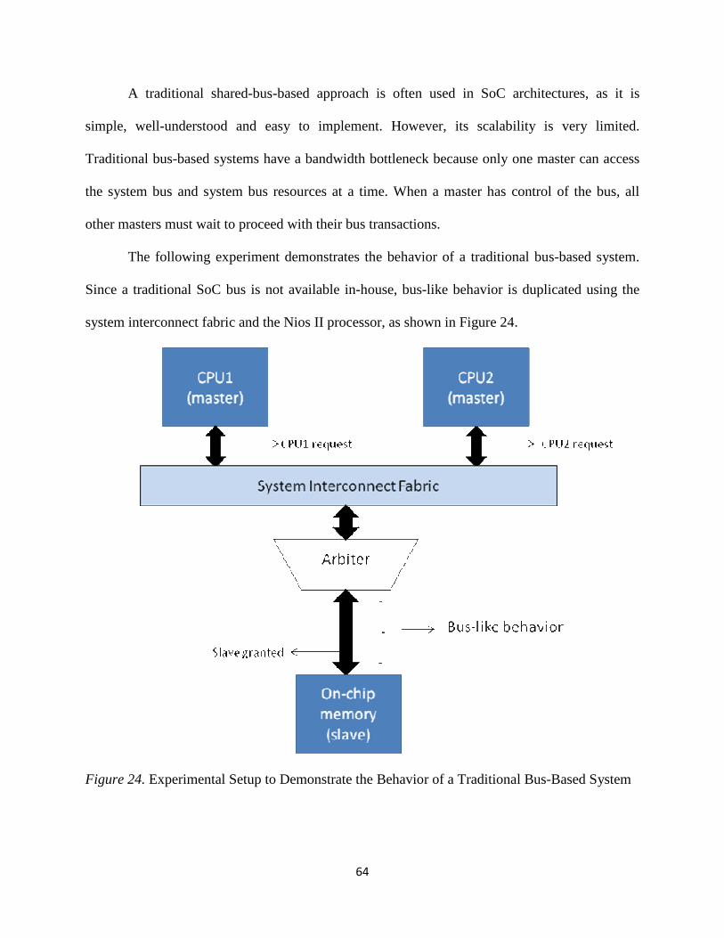
64
A traditional shared-bus-based approach is often used in SoC architectures, as it is
simple, well-understood and easy to implement. However, its scalability is very limited.
Traditional bus-based systems have a bandwidth bottleneck because only one master can access
the system bus and system bus resources at a time. When a master has control of the bus, all
other masters must wait to proceed with their bus transactions.
The following experiment demonstrates the behavior of a traditional bus-based system.
Since a traditional SoC bus is not available in-house, bus-like behavior is duplicated using the
system interconnect fabric and the Nios II processor, as shown in Figure 24.
Figure 24. Experimental Setup to Demonstrate the Behavior of a Traditional Bus-Based System

65
Although the system interconnect fabric uses multiple connection paths and slave-side
arbitration, described in section 5.2.2, the connection between the arbiter and the shared slave
behaves like a traditional time-shared bus. When CPU1 and CPU2 request the slave
simultaneously, the access to the slave is arbitrated, and only one CPU is granted access to the
slave at a given time. The waveform in Figure 25 demonstrates this behavior. The first two
signals in Figure 25 are the requests made by CPU1 and CPU2 respectively, for the on-chip
memory slave. The third signal is the granted signal on the on-chip memory slave side.
Figure 25. Master request and Slave granted Signals Demonstrating Bus-like Behavior
Between time 0 and time 48, there are 10 requests generated by each master. Hence, there
are a total of 20 requests made for the “bus” between time 0 and time 48, but the slave is granted
only 10 times. This demonstrates that although both masters request access to the “bus”, only
one of them gets access to it at a given time, and all requests cannot be granted. The following

66
sections explain the advantages of the system interconnect fabric over traditional bus-based
architectures.
5.2.2 Slave-Side Arbitration
The slave-side arbitration and multiple communication paths used by the system
interconnect fabric increase system bandwidth by reducing the bottleneck caused by bus-side
arbitration for the single communication path. In slave-side arbitration, bus masters contend for
individual slaves, not for the bus itself. It is called slave-side arbitration because it is
implemented at the point where two or more masters contend for the same slave. Every slave
peripheral that can be accessed by multiple masters has an arbitrator. Multiple masters can be
active at the same time, simultaneously transferring data with independent slaves using different
communication paths within the partial crossbar. However, if two or more masters initiate a
transfer with the same slave in the same clock cycle, the arbiter dictates which master gains
access to the slave through the shared communication path. For example, Figure 26 demonstrates
a system with two masters (a CPU and a DMA controller) sharing a slave (Data memory).
Arbitration is performed at the memory slave. Additional communication paths provided by the
partial crossbar are shown among the various system components. For the shared
communication path with the data memory slave, the arbiter dictates which master gains access
to the slave if both masters initiate a transfer with the slave in the same cycle.

67
Figure 26. Slave-Side Arbitration
Figure 27 shows additional detail of the data, address, and control paths in the connection
between two masters and the shared slave. The arbiter logic multiplexes all address, data, and
control signals from a master to a shared slave. In this way, the fabric will provide independent
communication channels to all slaves from all masters. But at the arbiter, the independent paths
are combined to a single, shared communication path that interfaces directly with the shared
slave. This design makes the slave interface to the fabric standard and only the fabric and
arbiter, which is part of the fabric, change as masters and slaves are added or removed from the
system.

68
Figure 27. Multimaster Connections on the System Interconnect Fabric (Altera Corporation, 2009)
The arbiter logic performs the following functions for its slave:
• Evaluates the address and control signals from each master and determines which master,
if any, gains access to the slave next.
• Grants access to the chosen master and forces all other requesting masters to wait by
inserting wait-states.
• Uses multiplexers to connect address, control, and datapaths between multiple masters
and the slave.
Figure 28 shows the arbiter logic in an example multimaster system with two masters, each
connected to two slaves.

69
Figure 28. Arbiter Logic on the System Interconnect Fabric (Altera Corporation, 2009)
5.3 Demonstrating True Concurrency Using the Partial Crossbar Fabric
The system interconnect fabric allows multiple masters to perform transfers
simultaneously with independent slaves. This concurrent communication capability is a unique
feature of the crossbar structure used by the system interconnect fabric, as opposed to traditional
shared-bus architectures. This architecture can achieve true concurrency resulting in a great
throughput performance advantage compared to traditional buses. The throughput improvement
depends on how often the multiple masters in the system are active simultaneously to non-shared
slaves.

70
Figure 29 shows a block diagram of an SOPC Builder system used to demonstrate true
concurrency of the system interconnect fabric, using I/O devices as slaves. Two Nios II/s CPU
cores provide the masters in the system and on-board LED banks are used as independent slaves.
The two LED banks are named LEDS and PIO respectively in the SOPC Builder.
Figure 29. SOPC Builder System with Independent I/O Slaves
Appendix C contains the Nios II assembly language programs executing on the two
masters to drive the two LED banks independently. The programs turn an LED on and off
rapidly and continuously, thus generating continuous requests across the fabric to access the
slave. The response of the slaves is captured using the SignalTap II Embedded Logic Analyzer.
The two slaves are found to respond simultaneously, during the exact same clock cycle. Figure
30 is a screenshot of the data captured on SignalTap II for this experiment.
The waitrequest signal is an input signal to the CPU data master. This signal, generated
by the system interconnect fabric, forces the master to wait until the fabric is ready to proceed

71
with the transfer. The chipselect and granted are slave-side signals internal to the fabric and not
available on the slave port. The granted indicates that arbitration has granted slave-access to a
requesting master. The chipselect is associated with off-chip I/O peripherals and indicates that
the slave peripheral is being accessed by a master in the system.
Figure 30. Concurrent Communications with I/O Slaves
The above waveform shows that at time 3, the chipselect and granted signal for both
slaves is asserted at the exact same instance. This indicates that both masters are granted access
to their respective slave at the exact same time, and data is being transferred simultaneously to

72
both slaves. This is observed again at time 9, time 15, and time 21. It is thus demonstrated that
the two Nios II CPUs are able to access the two on-board LED banks concurrently due to the
crossbar nature of the system interconnect fabric.
Figure 31 is a block diagram of a system that is used to demonstrate true concurrency on
the system interconnect fabric using on-chip memory slaves. Two Nios II/s CPU cores are the
two masters in the system and on-chip memories are used as two independent slaves.
Figure 31. SOPC Builder System with Independent Memory Slaves
Appendix C contains the Nios II assembly language programs executing on the two
masters. Both the programs perform a single write operation to a memory location within their
respective slave memory space and then enter a loop that reads the value from that location
continuously. This generates continuous read requests to the slaves. The response of the slaves to
the read requests is captured using the SignalTap II Logic Analyzer. Figure 32 is a snapshot of

73
the SignalTap II data. CPU1 reads the binary value 00111100 (60 in decimal) and CPU2 reads
value 11000011 (195 in decimal) continuously from its respective memory slave.

74
Figure 32. Concurrent Communications with Memory Slaves

75
The waveform in Figure 32 shows that at time 4, the chipselect and granted signals for
both slaves are asserted at the exact same instance. The data 00111100 and 11000011 appear on
the readdata lines on the same clock edge. This indicates that both CPUs are granted access to
their respective slaves at the exact same time and data is being transferred simultaneously from
both slaves. This is observed again at times 10, 16, 22, 34, 40 and 46. It is thus demonstrated that
the two Nios II CPUs are able to access the two on-chip memory components concurrently due
to the crossbar nature of the system interconnect fabric.
The above two experiments demonstrate true concurrency on the system interconnect
fabric. Such concurrency would not be possible in a traditional bus-based system because in bus-
based systems, a single communication link is shared by all the masters in the system. If two
masters request access to two different slaves simultaneously, only one master can use the bus at
a given time and the other master is forced to wait. The crossbar nature of the system
interconnect fabric is thus advantageous over a traditional shared-bus as it allows for
simultaneous transfers between different master-slave pairs.
5.4 Throughput Improvement
It has been demonstrated that the system interconnect fabric allows multiple masters to
transfer data concurrently to independent slaves. This results in true concurrency and increased
throughput. Throughput is defined as the number of transfers per unit time. Since concurrent
transfers are possible, more transfers can be achieved per unit time, if multiple masters and
multiple slaves are active simultaneously. The following experiment demonstrates the
improvement in throughput achieved by concurrent transfers on the system interconnect fabric.

76
Figure 33 shows the block diagram of a SOPC system with one CPU and one slave. The
master is part of the Nios II/s CPU and on-chip memory is the slave. The CPU generates
continuous read requests to the slave and the response of the slave is captured using the
SignalTap II Logic Analyzer. The Nios II assembly language code used for this is listed in
Appendix C.
Figure 33. Experimental Setup with One CPU and One Slave to Investigate Throughput
Figure 34 shows the SignalTap screen capture for the response of this system. The master
continuously requests access to the slave. It is noted that between time 0 and time 56, ten
requests are generated by the master and the slave granted signal is asserted ten times,
representing ten transfers in 56 clock cycles.

77
Figure 34. Response of the System with One CPU and One Slave for Throughput Investigation
The throughput of a bus-based system can be obtained from the bus-like behavior of the
system as described in Section 5.2.1. Figure 35 shows the SignalTap II capture for the response
of this system. It is noted that between time 0 and time 56 each master requests the slave twelve
times. Hence a total of twenty four requests are generated. But the slave granted signal is
asserted only twelve times, representing twelve transfers in 56 clock cycles. The one-CPU-one-
slave system generates fewer requests over the test time than the bus-based system, but all ten of
those requests are serviced within the test time. The bus-based system generates more requests,
but only half of those are serviced within the test time.

78
Figure 35. Response of a Bus-Based System for Throughput Investigation
Now, the architecture in Figure 36 is considered. Two Nios II/s CPUs provide the masters
in the system and two independent on-chip memory components are used as the slaves. Each
master is connected to one slave only, thus allowing them to transfer data simultaneously. The
masters execute the same program as in the earlier single CPU-slave experiment. The masters
generate continuous read requests to their respective slaves and the response of the slaves is
captured using the SignalTap II Logic Analyzer.

79
Figure 36. Experimental Setup with Two CPUs and Two Slaves to Investigate Throughput
Figure 37 shows the SignalTap screen capture for the response of this system. It is noted
that between time 0 and time 56, ten requests are generated by each master. The granted signal
for the slave 1 is asserted ten times and that for slave 2 is also asserted ten times. Hence, there
are twenty grants asserted between time 0 and 56. Therefore, twenty data transfers take place in
56 clock cycles as opposed to ten transfers with one CPU-slave pair, and twelve transfers with a
shared-bus between two CPUs.

80
Figure 37. Response of the System with Two Masters and Two Independent Slaves for Throughput Investigation
It is thus demonstrated that the throughput is substantially increased when two
independent master-slave pairs are active in the system. This is only possible due to the
concurrency supported by the crossbar nature of the system interconnect fabric. The amount of
improvement in throughput depends on how often the system application needs multiple masters
in the system to be active simultaneously with non-shared slaves.

81
5.5 Fairness-Based Arbitration Shares
When multiple masters contend for access to a shared slave on the system interconnect
fabric, the arbiter grants shares in round-robin order. Round-robin means that every master gets
equal number of shares in a circular order without priority. An arbitration share is an integer
value associated with the master with respect to a slave. One share represents permission to
perform one transfer (Altera Corporation, 2009). So, arbitration shares provide a way to allocate
access to a shared slave. The user can specify arbitration shares for each master in the SOPC
Builder. Masters can be assigned equal access to the slave by assigning all masters the same
number of shares. Also, one master can be given extra access by assigning it a larger number of
shares than the other masters. For every transfer, only requesting masters are included in the
arbitration.
Arbitration shares between a master-slave pair can be specified using the Connections
Matrix in the SOPC Builder System Contents tab. The arbitration settings are hidden by default,
but can be seen by clicking on the View menu and then on Show Arbitration, as shown in
Figure 38.
Figure 38. Arbitration Share Settings in the SOPC Builder Connections Matrix

82
To better understand how arbitration shares work, following example can be considered.
Suppose two masters issue simultaneous requests to access a single shared slave. Master 1 is
assigned five shares on the slave and Master 2 is assigned one share. This means that Master 1 is
allowed to execute up to five consecutive transfers with the slave, and Master 2 is required to
wait until these five transfers are completed. Master 2 may then execute one transfer with the
slave. After this, the arbiter goes back to check if Master 1 has any transfers to make. If so,
Master 1 is again allowed to make up to five transfers. This cycle repeats itself as long as both
masters keep requesting transfers to the same slave. In this way, Master 1 is allocated five of
every six transfers with the slave, if needed, representing 83.3% of all transfers with the slave.
However, if a master stops requesting transfers before it exhausts its shares, it forfeits all its
remaining shares, and the arbiter grants access to another requesting master. So, if Master 1 only
needs four transfers, then it gives up its fifth share to Master 2, which gets a supply of two
shares, if needed.
To demonstrate the behavior of the arbitration shares, a test was performed. Figure 39
shows a block diagram of an SOPC Builder system used to examine the behavior of arbitration
shares. In this system, two CPUs share a common memory slave, so that the access to the slave is
arbitrated.

83
Figure 39. SOPC Builder System Used to Examine the Behavior of Arbitration Shares
Nios II/s CPU cores provide the masters and on-chip memory is the slave. Both CPUs are
given one arbitration share (1:1 shares). CPU1 first writes two different values in two different
fixed on-chip memory locations. CPU1 and CPU2 then read the respective values continuously
from those locations. Appendix C contains the Nios II assembly program used for this. CPU1
reads the binary data 00111100 (60 in decimal) and CPU2 reads the binary data 11000011 (195
in decimal). When observed using the SignalTap II Logic Analyzer, CPU1 and CPU2 can be
observed reading the values alternately, in a round-robin manner, as seen in the waveform in
Figure 40.

84
Figure 40. Output Waveforms with 1:1 Arbitration Shares

85
The waitrequest signals for CPU1 and CPU2 are asserted for the same duration of time,
which is 4 clock cycles as seen in Figure 40. This indicates that both CPUs get equal amount of
access time to the slave. That is, they have equal arbitration shares (1:1) with respect to the
slave.
The arbitration shares for CPU2 were then increased to 10 (1:10 shares) and the same
program was executed again. It was expected that since CPU2 has more shares than CPU1, more
transfers by CPU2 would be seen. But this was not observed. The output of this experiment was
the exact same waveform as Figure 40, despite the increased shares of CPU2. The same
experiment was repeatedly performed with 10:1, 1:100 and 100:1 arbitration shares, but no
change was observed in the output waveform. While attempting to explain this puzzling
behavior, it was discovered that the shares are not observed because the requests by the two
CPUs do not occur in the same clock cycle (Altera Corporation, 2008). Since the CPU1 request
comes before the CPU2 request, it is serviced first and the CPU2 request is serviced next. The
next request from CPU1 comes only after the servicing of CPU2 has already begun. Therefore,
there is no contention for the slave during the same clock cycle, and no arbitration is required. In
order to see the arbitration shares behavior, requests from two or more CPUs have to be
generated in the same clock cycle.
The two CPUs in the above experiments execute the exact same code, except for reading
from different memory locations within the same on-chip memory component. In order to
increase the chance of the CPUs generating read requests in the same clock cycle, the following
efforts were made:
1. The CPUs read from memory continuously in a loop, using the Load Byte (ldb)
instruction. The number of ldb instructions that the CPU executes before branching back

86
to the top of the read loop was increased drastically. This reduces the chances of a
“branch” of one CPU coinciding with a “read” of the other CPU, and increases the
chances of the “read” of both CPUs coinciding at the clock-level. Appendix C contains
the assembly language program with a tight loop of 30 reads for each CPU.
2. The number of CPUs in the system is increased up to six. Each CPU reads continuously
from the memory in a tight loop of read instructions. Increased number of CPUs
increases the chances of concurrent requests.
Despite the above efforts, concurrent requests at the clock-level could not be achieved
and the behavior of arbitration shares could not be observed. Figure 41 shows the output
waveform for a system with six CPUs.

87
Figure 41. Output Waveform of a Six CPU System Performing Continuous Reads from the Same Memory Slave
It is observed that although each CPU reads continuously from the same memory slave,
no two CPUs generate read requests at the same clock cycle, thus eliminating the necessity for
arbitration. Therefore, the behavior of the arbitration shares is not observed.
The generation of precisely synchronized read requests is complicated by the pipelining
that is implemented on each CPU. The instruction pipelining obscures the boundaries between
requests making it even more difficult to synchronize at the clock level multiple requests for the
same slave. One other observation from this test should be mentioned. Since the precise

88
synchronization of multiple requests is so difficult to achieve, it is believed that true arbitration is
rarely performed within the fabric.

89
CHAPTER 6
CONCLUSIONS
6.1 Summary
In this project, the scalability of an on-chip partial crossbar interconnect and its
arbitration mechanism are analyzed experimentally. The partial crossbar interconnect considered
for experimentation is the system interconnect fabric created by Altera Corporation. A
multiprocessor SoC is created using Altera’s Nios II soft processor cores. The system
interconnect fabric which connects various components in this multiprocessor system, is
autogenerated by the SOPC Builder tool from Altera. The multiprocessor SoC including the
system interconnect fabric is realized on the Cyclone II EP2C35 FPGA device from Altera.
To analyze the scalability of the system interconnect fabric, the logic footprint of the
fabric is investigated based on experimental observations. First, the logic utilization of the fabric
is observed as more CPUs are added to the system. The increase in the logic utilization of the
fabric as the number of CPUs is increased from one to eight is found to be fairly linear. Next, the
logic utilization of the fabric is observed as more slaves are added to the system. The number of
slaves in the system is increased from one to eight. The increase in logic utilization by fabric,
although linear, is found to be significantly smaller than that associated with the addition of a
master. An equation is presented that is capable of representing the number of LEs required in
the system. Also, the logic utilization of the fabric is observed as exclusively connected CPU

90
slave pairs are added to the system incrementally from one to eight. It is determined that the data
collected for the CPU-slave pairs matches closely that which was predicted using the derived
equation. Therefore, the equation can be used as a predictive tool for designers, especially early
in the design cycle.
There is no direct data showing the number of LEs required for a traditional shared-bus
interconnection network. Therefore, direct comparisons are not possible. However, it is safe to
speculate that the system interconnect fabric does not scale well in comparison with traditional
shared-bus architectures in terms of logic resource utilization and the system cost. This
conclusion is expected given the nature of the partial crossbar interconnection network
implemented in the Altera system interconnect fabric.
The system interconnect fabric uses slave-side arbitration which is implemented when
two or more masters contend for the same slave. However, if two masters request to perform
transfers with two different slaves independently, the fabric allows these transfers
simultaneously, resulting in true concurrency. This concurrency leads to higher communication
bandwidth and is a unique feature of the crossbar structure used by the system interconnect
fabric compared to traditional shared-bus structures. The concurrency provided by the partial
crossbar fabric is experimentally demonstrated in this research with both memory and I/O slaves.
Transfers with two independent slaves are observed on the same rising clock edge, and thus true
concurrency of the fabric is proven. Such concurrency is not possible in bus-based systems due
to the shared nature of the interconnection. It is found that this true concurrency yields increased
throughput compared to a traditional bus-based system. In conclusion, the system interconnect
fabric is significantly advantageous over a traditional shared-bus architecture in terms of
communication bandwidth and system throughput.
91
The system interconnect fabric also uses fairness-based arbitration shares for multiple
masters accessing one slave. When the ratio of the shares is 1:1 both masters get one transfer to
the slave in a round-robin manner. For n:m shares, Master 1 gets n transfers and Master 2 gets m
transfers to the slave. To observe this behavior, it was necessary to generate simultaneous slave
requests from both masters, which proved to be very difficult to achieve experimentally.
6.2 Future Work
As with all research, the analysis presented in this thesis can be extended and improved
upon. Also, since multiprocessor SoC is a fairly new, emerging area of research it can be widely
explored using the analysis and information in this thesis as groundwork. There are two broad
areas in which this work can be enhanced: Performing further analysis on the existing
multiprocessor SoC architecture used in this research; and secondly creating various
multiprocessor networks-on-chip and analyzing their behavior.
First, it may be possible to generate simultaneous slave requests from multiple masters in
order to observe the fairness-based arbitration shares in the system interconnect fabric. This may
require technical support from Altera Corporation, since the system interconnect fabric is
autogenerated by an Altera tool. Also, timing analysis can be performed on the existing
architecture to verify if the system timing requirements are met by the design. The Altera
TimeQuest Timing Analyzer can be used for this purpose. Power analysis can be performed on
the existing design to determine the power consumption of the device. The effects of additional
CPUs and their software load on power consumption can be analyzed. Altera PowerPlay Power
Analyzer can be used for this. ModelSim simulation tool can be used together with PowerPlay to
simulate the software load on the CPUs for power analysis.
92
Another important enhancement to this research effort would be to implement a
centralized RTOS governing all the CPUs in the SoC. Altera provides support for MicroC/OS-II
RTOS and with the current architecture, it is easily possible to have an instance of MicroC/OS-II
executing on each of the CPUs in the system. However, it would require additional research to
implement a single instance of MicroC/OS-II governing all CPU activity in the SoC. This would
tremendously enhance this work from a real-world applications perspective.
Finally, the various network topologies such as star, ring, mesh, hypercube discussed in
Chapter 1 can be implemented on the FPGA using SOPC Builder. Their performance can be
documented using various software benchmark algorithms.

93
REFERENCES
Aldworth, P. J. (1999). System-on-a-Chip Bus Architecture for Embedded Applications.
International Conference on Computer Design, (pp. 297 - 298). Austin, TX.
Altera Corporation. (2009, April). Avalon Interface Specifications. Retrieved January 13, 2010,
from http://www.altera.com/literature/manual/mnl_avalon_spec.pdf
Altera Corporation. (2008, June). Avalon Memory-mapped Design and Optimizations. Retrieved
June 4, 2010, from http://www.altera.com/literature/hb/nios2/edh_ed51007.pdf
Altera Corporation. (2007). Creating Multiprocessor Systems using Nios II Tutorial . Retrieved
August 27, 2009, from http://www.altera.com/literature/tt/tt_nios2_multiprocessor_tutorial.pdf
Altera Corporation. (2005, July). Cyclone II Device Family Datasheet. Retrieved September 15,
2009, from http://www.altera.com/literature/hb/cyc2/cyc2_cii5v1_01.pdf
Altera Corporation. (2006). DE2 Development and Education Board User Manual. Retrieved
August 2, 2010, from ftp://ftp.altera.com/up/pub/Webdocs/DE2_UserManual.pdf
Altera Corporation. (2009, November). Design and Debugging using the SignalTap II Embedded
Logic Analyzer. Retrieved January 24, 2010, from Quartus II Handbook, Volume 3: Verification:
http://www.altera.com/literature/hb/qts/qts_qii53009.pdf
Altera Corporation. (2008). Nios II processor Reference Handbook. Retrieved August 13, 2009,
from http://www.altera.com/literature/hb/nios2/n2cpu_nii5v1.pdf
Altera Corporation. (2009). Nios II Processor Reference Handbook. Retrieved October 11, 2009,
from http://www.altera.com/literature/hb/nios2/n2cpu_nii5v1.pdf

94
Altera Corporation. (2008). Quartus II Handbook, Volume 1: Design and Synthesis. Retrieved
August 20, 2009, from http://www.altera.com/literature/hb/qts/qts_qii5v1_03.pdf
Altera Corporation. (2008). Quartus II Handbook, Volume 4: SOPC Builder. Retrieved August
2, 2009, from http://www.altera.com/literature/hb/qts/qts_qii5v4_03.pdf
Altera Corporation. (2008). SOPC Builder user Guide. Retrieved December 15, 2008, from
http://www.altera.com/literature/hb/qts/qts_qii54003.pdf
Altera Corporation. (2009, November). System Interconnect fabric for Memory-mapped
Interfaces. Retrieved January 13, 2010, from Quartus II Handbook, Volume 4: SOPC Builder:
http://www.altera.com./literature/qtsii_v1_03.pdf
Benini, L., & De Micheli, G. (2002). Networks on Chips: A New SoC Paradigm. Computer, 23
(2), 5-16.
Duncan, R. (1990). A Survey of Parallel Computer Architectures. Computer, 35 (1), 70-78.
Flynn, D. (1997). AMBA: Enabling Reusable on-chip designs. Micro, IEEE , 17 (4), 20-27.
Flynn, M. J. (1966). Very High Speed Computer Systems. Proceedings of the IEEE, 54, pp.
1901-1909.
Freescale Semiconductor. (2009, June). MSC8144 Quad Core Media Signal Processor Reference
Manual. Retrieved July 19, 2010, from
http://cache.freescale.com/files/dsp/doc/ref_manual/MSC8144RM.pdf
Goren, O., & Netanel, Y. (2006). High performance on-chip Interconnect system supporting fast
SoC generation. International Symposium on VLSI Design, Automation and Test, (pp. 1-4).
Hamblen, J. O., Hall, T. S., & Furman, M. D. (2008). Rapid Prototyping of Digital Systems.
Springer Science+Business Media, LLC.
Jerraya, A. A., & Wolf, W. (2005). Multiprocessor System-on-Chips. Morgan Kauffman
Publishers.
95
Lahiri, K., Raghunathan, A., & Dey, S. (2001). Evaluation of the Traffic-Performance
Characteristics of System-on-chip communication architectures. The 14th International
Conference on VLSI Design, (pp. 29-35).
Null, L., & Lobur, J. (2006). Computer Organization and Architecture. Sudbury, Massachusetts,
Jones and Bartlett Publishers.
Pande, P. P., Grecu, C., Jones, M., Ivanov, A., & Saleh, R. (2004). Evaluation of MP-SoC
interconnect architectures: A case study. 4th IEEE International Workshop on System-on-Chip
for Real-Time Applications, (pp. 253-256).
Ruggiero, M., Angiolini, F., Poletti, F., & Bertozzi, D. (2004). Scalabilty Analysis of Evolving
SoC Interconnect protocols. International Symposium on Systems-on-Chip, (pp. 169-172).
Xilinx, Inc. (2010). MicroBlaze Soft Processor Core Product Specifications. Retrieved July 19,
2010, from http://www.xilinx.com/tools/microblaze.htm
Xilinx, Inc. (2008). MicroBlaze processor Reference Guide. Retrieved July 19, 2010, from
http://www.xilinx.com/support/documentation/sw_manuals/mb_ref_guide.pdf
Zhang, Y., & Irwin, M. J. (1999). Power and Performance Comparison of Crossbars and Buses
as On-chip interconnect structures. Thirty-Third Asilomar Conference on Signals, Systems, and
Computers, 1, pp. 378-383.

96
APPENDIX A
This appendix provides step-by-step instructions for creating a multiprocessor system-on-
chip using the Nios II processor on the DE2 board.
A.1 Hardware and Software Requirements
This document is written for the following software and hardware platform:
Quartus II Development Software version 8.0
Nios II IDE version 8.0
Altera DE2 board
USB blaster cable
Later versions of these software tools may be used, but the GUI in those versions may be slightly
different. This document can still be used as a reference.
A.2 To Begin
Altera’s tutorial for creating multiprocessor systems with Nios II is available on the
Altera website at http://www.altera.com/literature/tt/tt_nios2_multiprocessor_tutorial.pdf. This
tutorial is written for the Nios Development Kit and cannot be followed exactly for the DE2
board. For the DE2 board, it can be used it as a reference in combination with the information

97
from the textbook “Rapid Prototyping of Digital Systems – SOPC Edition” by J. O. Hamblen.
Some other Altera documentation is also required, which are mentioned later in this appendix.
Before proceeding with creating multiprocessor systems, it would help to be familiar with
building a basic Nios II system as described in Chapter 16 and 17 of the above-mentioned
textbook by J. O. Hamblen. The user should have successfully tested the two examples provided
in those chapters: rpds_sofware and rpds_test. The design in Chapter 17 of the book can be used
as a starting point for creating multiprocessor systems.
Nios II multiprocessor systems are split into two main categories: those that share
resources, and those in which each processor is independent and does not share resources with
other processors. This is described in detailed in the above-mentioned tutorial by Altera. The
user should be familiar with this background before proceeding with creating the systems in
hardware. Following is the step-by-step procedure to build a multiprocessor system with two
CPUs that share a memory component.
A.3 Creating a SOPC System with two CPUs
The design in Chapter 17 from the textbook by J.O. Hamblen is used here as a starting
point. First, build a Nios II system as described in detail in Chapter 17. Alternatively, CHAP 17
folder from the DVD accompanying the book can be used. This folder contains the design that is
described in Chapter 17.
1. For this design, switch 9 on the DE2 board is the RESET switch and must always be ON
Turn on switch 9 (UP position).

98
2. Suppose CHAP 17 folder is copied to the location C:/Project. Rename that to
CHAP17_multi_cpu. So, the working directory path would be
C:/Project/CHAP17_multi_cpu
3. Open the Quartus Project File (rpds17.qpf) for this project and then open the SOPC
Builder tool.
4. In SOPC Builder, right click on cpu component and click Rename. Rename the
processor as cpu1.
5. Then right click timer0 and rename it to cpu1_timer.
6. If cpu1_timer is not immediately under cpu1, right click on it and click Move Up several
times to move it under cpu1.
7. In the list of available components on the left-hand side of the System Contents tab,
select Nios II Processor. Click Add.
8. The Nios II Processor MegaWizard interface appears, displaying the Nios II Core page.
Specify the settings as shown in Figure A.1

99
Figure A.1 Nios II Processor MegaWizard
9. Note that the Reset Vector and Exception Vector have been changed to SDRAM from
SRAM. In the multi-CPU system, the program memory will have to be partitioned
between the two CPUs (Read page 1-10 of the Altera tutorial). The on-board SRAM is
only 512 MBytes and may not be enough to execute the software on multiple CPUs.
Therefore SDRAM which is 8Mbytes is needed.
10. The SDRAM is partitioned into exactly two halves, 4MB for each CPU. Hence, Reset
and Exception Vector offsets are set to 0x400000 and 0x400020.
11. Click JTAG Debug Module. The JTAG Debug Module page appears. Select Level 1 as
the debugging level for this processor. Click Finish.

100
12. Right-click the newly-added processor and rename it to cpu2. Right click and Move Up
cpu2 under cpu1_timer.
13. Add an interval timer from the available list of components under Peripherals >
Microcontroller Peripherals > Interval Timer. Click Add. The Interval Timer
MegaWizard interface appears. In the Presets list, select Full-featured. Click Finish.
14. Right click on the newly added timer and rename it to cpu2_timer. Right click and Move
Up cpu2_timer under cpu2.
15. Using the connection matrix, connect cpu1_timer to the data master for cpu1 only and
cpu2_timer to the data master for cpu2 only.
16. Type 0 in the IRQ column for the cpu1/cpu1_timer connection and also for
cpu2/cpu2_timer connection. This value allows the respective timers to interrupt the
CPUs with a priority setting of 0, which is the highest priority.
17. From the available list of components under Peripherals > Debug and Performance,
add the System ID peripheral.
18. It is essential to include a hardware mutex component to protect that memory that is
shared between the processors from data corruption. In the list of available components,
under Peripherals > Multiprocessor Coordination, click Mutex. Click Add. The
Mutex MegaWizard interface appears.
19. Click Finish to accept the defaults. Right-click and rename the mutex as
message_buffer_mutex.
20. On-chip memory is shared by all processors in the system. The processors use the mutex
core added in the previous steps to protect the memory contents from corruption. In the
list of available components, Memories and Memory Controllers > On-Chip, click

101
On-Chip Memory (RAM or ROM). Click Add. The On-Chip Memory (RAM or ROM)
MegaWizard interface appears.
21. In the Total memory size box, type 1 and select KBytes to specify a memory size of 1
KByte. Click Finish.
22. Right-click onchip_mem and rename it as message_buffer_ram.
23. All the resources that are shared between processors in the system must be connected
properly using SOPC Builder's connection matrix and IRQ connection matrix.
24. Ensure that each cpu_timer is connected only to the data master for its CPU component.
25. Connect sdram to the instruction and data masters for each processor, allowing both
processors to access the sdram. All the connection dots for sdram should be solid black.
26. Connect message_buffer_mutex to the data masters for both processors and disconnect
both instruction masters, allowing both processors to access message_buffer_mutex.
27. Connect message_buffer_ram to the data masters for both processors and disconnect both
instruction masters, allowing both processors to access message_buffer_ram only as data
memory. No software instructions run from this ram.
28. Ensure that jtag_uart is only connected to the data master of cpu1.
29. Ensure that IRQs for both timer/cpu connections are 0 as mentioned above and that for
jtag_uart/cpu1 connection is 1.
30. On the System menu, click Auto-Assign Base Addresses to give every peripheral a
unique base address.
Figure A.2 shows a snapshot of the system after all the connections have been made.

102
Figure A.2 Shared Resource Connections in SOPC Builder
31. Note that flash, ext_bus, uart, leds, buttons, switches, lcd, sram are not used in this
example, so their connections don’t matter. But it is advisable to keep it consistent with
the above snapshot in order to avoid address conflicts. They can also be deleted if not
needed for future use.
32. In the System Generation tab, turn off Simulation and click Generate. When generation
is complete, a SUCCESS: SYSTEM GENERATION COMPLETED message is
displayed. This may take a few minutes.
33. Return to Quartus II. Click Start Compilation under the Processing menu. This also
takes a few minutes. After full compilation is successful go to the Tools menu, click
Programmer and download the *.sof file to the target device on the DE2 board.

103
34. The hardware part of this project is ready. Now software applications to run on these two
CPUs must be created.
A.3 Creating Software for the multiprocessor systems
Open the Nios II IDE. In the File menu click on Switch Workspace and change
workspace to C:/Projects/CHAP17_multi_cpu/software. All the software files related to this
project will be under this folder.
The step-by-step procedure for creating and running software projects is described
accurately in the Altera tutorial mentioned in section A.1. Follow the steps described in the
tutorial accurately to create software for cpu1 and cpu2. Give different name to the software
projects for cpu1 and cpu2. E.g. hello_world_multi1 and hello_world_multi2.
The sample program hello_world_multi.c is needed for the tutorial, which can be found
by searching www.altera.com. Select SDRAM as program memory, heap/ stack, read/write
memory and read-only memory in the System Library, as mentioned in the tutorial. Build the
two software projects, set up Nios II IDE to allow running multiple sessions and then run it as
described in the tutorial. If it runs successfully, the following messages should print continuously
to the console:
Hello from task1
Hello from task2
If these messages do not appear, there may be a problem related to tuning of the PLL.

104
A.4 Tuning the PLL
The textbook by Hamblen describes (Chapter 17, Pg 366) that a PLL is required for the
operation of the SDRAM. It has been added to the design. There is an IMPORTANT NOTE on
page 368 which says, “if the programs downloaded to the SDRAM do not verify, after double
checking that everything else in the design is right, the PLL phase shift may need to be adjusted
by a small amount. Most designs seem to fall within about 30 degrees of -54 degrees (which is
the phase shift in our current design). This corresponds to a time delay adjustment of only 1 or 2
ns.”
Hence, if this design is not successful, a PLL phase shift adjustment may be necessary.
Phase shift can be tuned on a trial-and-error basis a few times, since the variation is only in the
range of 1 to 2 ns. More information on tuning the PLL can be found in the Altera Nios II
Embedded Peripherals User Guide at
http://www.altera.com/literature/hb/nios2/n2cpu_nii5v3_01.pdf
A.5 Building Independent Multiprocessor Systems
Procedure for building independent multiprocessor systems will be the same as above but
the mutex and message_buffer_ram components will not be needed. All the IO peripherals
must be connected to only one CPU as Altera does not allow sharing on non-memory peripherals
by multiple masters.
Two different applications will have to execute on the two CPUs. For example, one of the
CPUs can print “Hello World” to the console and the other can blink an LED. JTAG_UART is
used to print to the console and it is a non-memory peripheral which must only be connected to

105
one CPU. Hence, both CPUs cannot print to the console without sharing memory. Building
independent systems should be extremely easy after having built a shared memory system.

106
APPENDIX B
This appendix lists the VHDL declarations of the fabric components associated with the
addition of a new CPU and a new memory slave in the SOPC system. These components are:
a. cpu_data_master_arbitrator
b. cpu_instruction_master_arbitrator
c. cpu_jtag_debug_module_arbitrator
d. onchip_memory_arbitrator (Slave-side arbiter)
B.1 VHDL declarations for cpu_data_master_arbitrator
entity cpu1_data_master_arbitrator is
port (
-- inputs:
signal clk : IN STD_LOGIC;
signal cpu1_data_master_address : IN STD_LOGIC_VECTOR (24 DOWNTO 0);
signal cpu1_data_master_byteenable_sdram_s1 : IN STD_LOGIC_VECTOR (1
DOWNTO 0);
signal cpu1_data_master_granted_cpu1_jtag_debug_module : IN STD_LOGIC;
signal cpu1_data_master_granted_jtag_uart_avalon_jtag_slave : IN STD_LOGIC;
signal cpu1_data_master_granted_onchip_mem_s1 : IN STD_LOGIC;
signal cpu1_data_master_granted_sdram_s1 : IN STD_LOGIC;
107
signal cpu1_data_master_qualified_request_cpu1_jtag_debug_module : IN
STD_LOGIC;
signal cpu1_data_master_qualified_request_jtag_uart_avalon_jtag_slave : IN
STD_LOGIC;
signal cpu1_data_master_qualified_request_onchip_mem_s1 : IN STD_LOGIC;
signal cpu1_data_master_qualified_request_sdram_s1 : IN STD_LOGIC;
signal cpu1_data_master_read : IN STD_LOGIC;
signal cpu1_data_master_read_data_valid_cpu1_jtag_debug_module : IN
STD_LOGIC;
signal cpu1_data_master_read_data_valid_jtag_uart_avalon_jtag_slave : IN
STD_LOGIC;
signal cpu1_data_master_read_data_valid_onchip_mem_s1 : IN STD_LOGIC;
signal cpu1_data_master_read_data_valid_sdram_s1 : IN STD_LOGIC;
signal cpu1_data_master_read_data_valid_sdram_s1_shift_register : IN STD_LOGIC;
signal cpu1_data_master_requests_cpu1_jtag_debug_module : IN STD_LOGIC;
signal cpu1_data_master_requests_jtag_uart_avalon_jtag_slave : IN STD_LOGIC;
signal cpu1_data_master_requests_onchip_mem_s1 : IN STD_LOGIC;
signal cpu1_data_master_requests_sdram_s1 : IN STD_LOGIC;
signal cpu1_data_master_write : IN STD_LOGIC;
signal cpu1_data_master_writedata : IN STD_LOGIC_VECTOR (31 DOWNTO 0);
signal cpu1_jtag_debug_module_readdata_from_sa : IN STD_LOGIC_VECTOR (31
DOWNTO 0);
signal d1_cpu1_jtag_debug_module_end_xfer : IN STD_LOGIC;

108
signal d1_jtag_uart_avalon_jtag_slave_end_xfer : IN STD_LOGIC;
signal d1_onchip_mem_s1_end_xfer : IN STD_LOGIC;
signal d1_sdram_s1_end_xfer : IN STD_LOGIC;
signal jtag_uart_avalon_jtag_slave_irq_from_sa : IN STD_LOGIC;
signal jtag_uart_avalon_jtag_slave_readdata_from_sa : IN STD_LOGIC_VECTOR
(31 DOWNTO 0);
signal jtag_uart_avalon_jtag_slave_waitrequest_from_sa : IN STD_LOGIC;
signal onchip_mem_s1_readdata_from_sa : IN STD_LOGIC_VECTOR (31
DOWNTO 0);
signal registered_cpu1_data_master_read_data_valid_onchip_mem_s1 : IN
STD_LOGIC;
signal reset_n : IN STD_LOGIC;
signal sdram_s1_readdata_from_sa : IN STD_LOGIC_VECTOR (15 DOWNTO 0);
signal sdram_s1_waitrequest_from_sa : IN STD_LOGIC;
-- outputs:
signal cpu1_data_master_address_to_slave : OUT STD_LOGIC_VECTOR (24
DOWNTO 0);
signal cpu1_data_master_dbs_address : OUT STD_LOGIC_VECTOR (1 DOWNTO
0);
signal cpu1_data_master_dbs_write_16 : OUT STD_LOGIC_VECTOR (15
DOWNTO 0);
signal cpu1_data_master_irq : OUT STD_LOGIC_VECTOR (31 DOWNTO 0);
signal cpu1_data_master_no_byte_enables_and_last_term : OUT STD_LOGIC;
109
signal cpu1_data_master_readdata : OUT STD_LOGIC_VECTOR (31 DOWNTO 0);
signal cpu1_data_master_waitrequest : OUT STD_LOGIC
);
end entity cpu1_data_master_arbitrator;
B.2 VHDL declarations for cpu_instruction_master_arbitrator
entity cpu1_instruction_master_arbitrator is
port (
-- inputs:
signal clk : IN STD_LOGIC;
signal cpu1_instruction_master_address : IN STD_LOGIC_VECTOR (24 DOWNTO
0);
signal cpu1_instruction_master_granted_cpu1_jtag_debug_module : IN STD_LOGIC;
signal cpu1_instruction_master_granted_sdram_s1 : IN STD_LOGIC;
signal cpu1_instruction_master_qualified_request_cpu1_jtag_debug_module : IN
STD_LOGIC;
signal cpu1_instruction_master_qualified_request_sdram_s1 : IN STD_LOGIC;
signal cpu1_instruction_master_read : IN STD_LOGIC;
signal cpu1_instruction_master_read_data_valid_cpu1_jtag_debug_module : IN
STD_LOGIC;
signal cpu1_instruction_master_read_data_valid_sdram_s1 : IN STD_LOGIC;
signal cpu1_instruction_master_read_data_valid_sdram_s1_shift_register : IN
STD_LOGIC;

110
signal cpu1_instruction_master_requests_cpu1_jtag_debug_module : IN
STD_LOGIC;
signal cpu1_instruction_master_requests_sdram_s1 : IN STD_LOGIC;
signal cpu1_jtag_debug_module_readdata_from_sa : IN STD_LOGIC_VECTOR (31
DOWNTO 0);
signal d1_cpu1_jtag_debug_module_end_xfer : IN STD_LOGIC;
signal d1_sdram_s1_end_xfer : IN STD_LOGIC;
signal reset_n : IN STD_LOGIC;
signal sdram_s1_readdata_from_sa : IN STD_LOGIC_VECTOR (15 DOWNTO 0);
signal sdram_s1_waitrequest_from_sa : IN STD_LOGIC;
-- outputs:
signal cpu1_instruction_master_address_to_slave : OUT STD_LOGIC_VECTOR (24
DOWNTO 0);
signal cpu1_instruction_master_dbs_address : OUT STD_LOGIC_VECTOR (1
DOWNTO 0);
signal cpu1_instruction_master_latency_counter : OUT STD_LOGIC;
signal cpu1_instruction_master_readdata : OUT STD_LOGIC_VECTOR (31
DOWNTO 0);
signal cpu1_instruction_master_readdatavalid : OUT STD_LOGIC;
signal cpu1_instruction_master_waitrequest : OUT STD_LOGIC
);
end entity cpu1_instruction_master_arbitrator;

111
B.3 VHDL declarations for jtag_debug_module_arbitrator
entity cpu1_jtag_debug_module_arbitrator is
port (
-- inputs:
signal clk : IN STD_LOGIC;
signal cpu1_data_master_address_to_slave : IN STD_LOGIC_VECTOR (24
DOWNTO 0);
signal cpu1_data_master_byteenable : IN STD_LOGIC_VECTOR (3 DOWNTO 0);
signal cpu1_data_master_debugaccess : IN STD_LOGIC;
signal cpu1_data_master_read : IN STD_LOGIC;
signal cpu1_data_master_waitrequest : IN STD_LOGIC;
signal cpu1_data_master_write : IN STD_LOGIC;
signal cpu1_data_master_writedata : IN STD_LOGIC_VECTOR (31 DOWNTO 0);
signal cpu1_instruction_master_address_to_slave : IN STD_LOGIC_VECTOR (24
DOWNTO 0);
signal cpu1_instruction_master_latency_counter : IN STD_LOGIC;
signal cpu1_instruction_master_read : IN STD_LOGIC;
signal cpu1_instruction_master_read_data_valid_sdram_s1_shift_register : IN
STD_LOGIC;
signal cpu1_jtag_debug_module_readdata : IN STD_LOGIC_VECTOR (31
DOWNTO 0);
signal cpu1_jtag_debug_module_resetrequest : IN STD_LOGIC;
signal reset_n : IN STD_LOGIC;

112
-- outputs:
signal cpu1_data_master_granted_cpu1_jtag_debug_module : OUT STD_LOGIC;
signal cpu1_data_master_qualified_request_cpu1_jtag_debug_module : OUT
STD_LOGIC;
signal cpu1_data_master_read_data_valid_cpu1_jtag_debug_module : OUT
STD_LOGIC;
signal cpu1_data_master_requests_cpu1_jtag_debug_module : OUT STD_LOGIC;
signal cpu1_instruction_master_granted_cpu1_jtag_debug_module : OUT
STD_LOGIC;
signal cpu1_instruction_master_qualified_request_cpu1_jtag_debug_module : OUT
STD_LOGIC;
signal cpu1_instruction_master_read_data_valid_cpu1_jtag_debug_module : OUT
STD_LOGIC;
signal cpu1_instruction_master_requests_cpu1_jtag_debug_module : OUT
STD_LOGIC;
signal cpu1_jtag_debug_module_address : OUT STD_LOGIC_VECTOR (8
DOWNTO 0);
signal cpu1_jtag_debug_module_begintransfer : OUT STD_LOGIC;
signal cpu1_jtag_debug_module_byteenable : OUT STD_LOGIC_VECTOR (3
DOWNTO 0);
signal cpu1_jtag_debug_module_chipselect : OUT STD_LOGIC;
signal cpu1_jtag_debug_module_debugaccess : OUT STD_LOGIC;

113
signal cpu1_jtag_debug_module_readdata_from_sa : OUT STD_LOGIC_VECTOR
(31 DOWNTO 0);
signal cpu1_jtag_debug_module_reset : OUT STD_LOGIC;
signal cpu1_jtag_debug_module_reset_n : OUT STD_LOGIC;
signal cpu1_jtag_debug_module_resetrequest_from_sa : OUT STD_LOGIC;
signal cpu1_jtag_debug_module_write : OUT STD_LOGIC;
signal cpu1_jtag_debug_module_writedata : OUT STD_LOGIC_VECTOR (31
DOWNTO 0);
signal d1_cpu1_jtag_debug_module_end_xfer : OUT STD_LOGIC
);
end entity cpu1_jtag_debug_module_arbitrator;
B.4 VHDL declarations for onchip_memory_arbitrator
entity onchip_mem_s1_arbitrator is
port (
-- inputs:
signal clk : IN STD_LOGIC;
signal cpu1_data_master_address_to_slave : IN STD_LOGIC_VECTOR (24
DOWNTO 0);
signal cpu1_data_master_byteenable : IN STD_LOGIC_VECTOR (3 DOWNTO 0);
signal cpu1_data_master_read : IN STD_LOGIC;
signal cpu1_data_master_waitrequest : IN STD_LOGIC;
signal cpu1_data_master_write : IN STD_LOGIC;

114
signal cpu1_data_master_writedata : IN STD_LOGIC_VECTOR (31 DOWNTO 0);
signal cpu2_data_master_address_to_slave : IN STD_LOGIC_VECTOR (24
DOWNTO 0);
signal cpu2_data_master_byteenable : IN STD_LOGIC_VECTOR (3 DOWNTO 0);
signal cpu2_data_master_read : IN STD_LOGIC;
signal cpu2_data_master_waitrequest : IN STD_LOGIC;
signal cpu2_data_master_write : IN STD_LOGIC;
signal cpu2_data_master_writedata : IN STD_LOGIC_VECTOR (31 DOWNTO 0);
signal onchip_mem_s1_readdata : IN STD_LOGIC_VECTOR (31 DOWNTO 0);
signal reset_n : IN STD_LOGIC;
-- outputs:
signal cpu1_data_master_granted_onchip_mem_s1 : OUT STD_LOGIC;
signal cpu1_data_master_qualified_request_onchip_mem_s1 : OUT STD_LOGIC;
signal cpu1_data_master_read_data_valid_onchip_mem_s1 : OUT STD_LOGIC;
signal cpu1_data_master_requests_onchip_mem_s1 : OUT STD_LOGIC;
signal cpu2_data_master_granted_onchip_mem_s1 : OUT STD_LOGIC;
signal cpu2_data_master_qualified_request_onchip_mem_s1 : OUT STD_LOGIC;
signal cpu2_data_master_read_data_valid_onchip_mem_s1 : OUT STD_LOGIC;
signal cpu2_data_master_requests_onchip_mem_s1 : OUT STD_LOGIC;
signal d1_onchip_mem_s1_end_xfer : OUT STD_LOGIC;
signal onchip_mem_s1_address : OUT STD_LOGIC_VECTOR (5 DOWNTO 0);
signal onchip_mem_s1_byteenable : OUT STD_LOGIC_VECTOR (3 DOWNTO 0);
signal onchip_mem_s1_chipselect : OUT STD_LOGIC;

115
signal onchip_mem_s1_clken : OUT STD_LOGIC;
signal onchip_mem_s1_readdata_from_sa : OUT STD_LOGIC_VECTOR (31
DOWNTO 0);
signal onchip_mem_s1_reset_n : OUT STD_LOGIC;
signal onchip_mem_s1_write : OUT STD_LOGIC;
signal onchip_mem_s1_writedata : OUT STD_LOGIC_VECTOR (31 DOWNTO 0);
signal registered_cpu1_data_master_read_data_valid_onchip_mem_s1 : OUT
STD_LOGIC;
signal registered_cpu2_data_master_read_data_valid_onchip_mem_s1 : OUT
STD_LOGIC
);
end entity onchip_mem_s1_arbitrator;

116
APPENDIX C
C.1 Nios II assembly language programs executing on two CPUs to drive two LED banks
independently
CPU1 code:
.section .text
.global main
main:
movhi r2,256 /*Create base address of LEDs*/
addi r2,r2,4096
movi r3,2
ledon: stwio r3,0(r2) /*Turn LED ON*/
stwio zero,0(r2) /*Turn LED OFF*/
beq zero, zero, ledon
CPU2 code:
.section .text
.global main
main:
addi r2,r2,4096 /*Create base address of LEDs*/
movi r3,2

117
ledon: stwio r3,0(r2) /*Turn LED ON*/
stwio zero,0(r2) /*Turn LED OFF*/
beq zero, zero, ledon
C.2 Nios II assembly language programs executing on two CPUs to access two different
memory banks independently
CPU1:
.section .text
.global main
main:
/*Create base address of memory*/
movhi r2,256
addi r2,r2,4096
/*Write binary value to base address*/
movi r3,60
stb r3,0(r2)
/*Read value from memory*/
read: ldb r4, 0(r2)
beq zero, zero, read
CPU2:
.section .text
.global main

118
main:
/*Create base address of memory*/
movi r2,4096
/*Write binary value to base address*/
movi r3,195
stb r3,0(r2)
/*Read value from memory*/
readhere: ldb r4, 0(r2)
beq zero, zero, readhere
C.3 Nios II assembly language program executing on one CPUs to access one memory bank
.section .text
.global main
main:
/*Create base address of memory*/
movhi r2,256
addi r2,r2,4096
/*Write binary value to base address*/
movi r3,60
stb r3,0(r2)
/*Read value from memory*/
read: ldb r4, 0(r2)
beq zero, zero, read
119
C.4 Nios II assembly language programs executing on multiple CPUs to access one memory
bank (for investigating arbitration)
The number of read instructions in the tight loop has been increased in order to increase
the possibility of concurrent requests to trigger arbitration.
.section .text
.global main
main:
/*Create base address for memory*/
movhi r2,256
addi r2,r2,4096
/*Write binary value to base address */
movi r4,60
stb r4,0(r2)
/*CPU1 reads value from base address of memory*/
read:
ldb r6, 0(r2)
ldb r6, 0(r2)
ldb r6, 0(r2)
ldb r6, 0(r2)
ldb r6, 0(r2)
ldb r6, 0(r2)
ldb r6, 0(r2)
ldb r6, 0(r2)

120
ldb r6, 0(r2)
ldb r6, 0(r2)
ldb r6, 0(r2)
ldb r6, 0(r2)
ldb r6, 0(r2)
ldb r6, 0(r2)
ldb r6, 0(r2)
ldb r6, 0(r2)
ldb r6, 0(r2)
ldb r6, 0(r2)
ldb r6, 0(r2)
ldb r6, 0(r2)
ldb r6, 0(r2)
ldb r6, 0(r2)
ldb r6, 0(r2)
ldb r6, 0(r2)
ldb r6, 0(r2)
ldb r6, 0(r2)
ldb r6, 0(r2)
ldb r6, 0(r2)
ldb r6, 0(r2)
ldb r6, 0(r2)
beq zero, zero, read


![HW-SW co-Design of an On-Chip IJTAG Dependability Processoressay.utwente.nl/70623/1/[Master Thesis] HW-SW co-Design of an On-Chip IJTAG... · pendability processor. An on-chip IJTAG](https://img.pdfslide.net/doc/110x75/5d31a73188c99342448bf57f/hw-sw-co-design-of-an-on-chip-ijtag-dependability-master-thesis-hw-sw-co-design.jpg)