Embed Size (px)
Citation preview
University of Nebraska - LincolnDigitalCommons@University of Nebraska - LincolnFaculty Publications from the Department ofElectrical and Computer Engineering Electrical & Computer Engineering, Department of
2014
An Isolated Multiport Bidirectional DC-DCConverter for PV-Battery-DC MicrogridApplicationsJianwu ZengUniversity of Nebraska-Lincoln, [email protected]
Wei QiaoUniversity of Nebraska–Lincoln, [email protected]
Liyan QuUniversity of Nebraska-Lincoln, [email protected]
Follow this and additional works at: http://digitalcommons.unl.edu/electricalengineeringfacpub
Part of the Computer Engineering Commons, and the Electrical and Computer EngineeringCommons
This Article is brought to you for free and open access by the Electrical & Computer Engineering, Department of at DigitalCommons@University ofNebraska - Lincoln. It has been accepted for inclusion in Faculty Publications from the Department of Electrical and Computer Engineering by anauthorized administrator of DigitalCommons@University of Nebraska - Lincoln.
Zeng, Jianwu; Qiao, Wei; and Qu, Liyan, "An Isolated Multiport Bidirectional DC-DC Converter for PV-Battery-DC MicrogridApplications" (2014). Faculty Publications from the Department of Electrical and Computer Engineering. Paper 332.http://digitalcommons.unl.edu/electricalengineeringfacpub/332
An Isolated Multiport Bidirectional DC-DC Converter for PV-Battery-DC Microgrid Applications
Jianwu Zeng, Wei Qiao*, and Liyan Qu Power and Energy Systems Laboratory Department of Electrical Engineering
University of Nebraska-Lincoln Lincoln, NE, 68588-0511 USA
[email protected]; [email protected]; [email protected]
Abstract—This paper proposes a new isolated, multiport, bidirectional DC-DC converter with the least number of switches for photovoltaic (PV)-battery-DC microgrid applications. The proposed converter is able to perform the maximum power point tracking (MPPT) control for the PV system when solar energy is available as well as control the charge and discharge of the battery with the PV system and the DC microgrid. Simulation and experimental studies are carried out and validate the proposed converter for simultaneous power management of a PV-battery system connected to a DC microgrid.
I. INTRODUCTION Microgrids are becoming a promising technology for
integrating distributed renewable energy systems and energy storage systems [1]. To integrate various renewable energy sources, such as photovoltaic (PV) systems and wind energy systems, and energy storage systems, such as batteries, into a microgrid, either a multiport converter for connecting multiple sources or an individual converter for each source can be used. A multiport converter is preferable to connect multiple sources to the grid or load due to their lower cost and higher power density.
A number of multiport converters have been proposed for renewable energy systems [2]-[9]. The multiport converter topologies can be classified into two categories: nonisolated topologies and isolated topologies. Nonisolated multiport converters are usually used in the applications which do not require galvanic isolation. In contrast, an isolated converter which contains a transformer is preferred for the applications which require galvanic isolation between the energy sources and the grid or load.
At some sites which are connected to a weak power grid or have no access to a power grid, renewable energy sources and energy storage systems are commonly used together. In
this case, a multiport bidirectional converter is preferable. The commonly used isolated multiport bidirectional DC-DC converters (BDCs) includes full-bridge [6] and half-bridge [7] topologies, which use two and four controllable switches for each port, respectively. However, the battery in [7] and [8] had to be charged and discharged within a switching period, i.e., the battery had to be charged and discharged with a high frequency, which is not desired from the perspective of the battery life. Recently, a new isolated three-port BDC was proposed for a PV-battery system [9]. That BDC used the least number of switches among all existing three-port BDCs, i.e., three switches for three ports, to realize the power management for the PV-battery system. The battery can be charged by the PV panel(s) and discharged to supply the load located on the high-voltage side (HVS) of the BDC. That BDC is preferable for standalone applications but is not sufficient for microgrid applications because the power flow between the LVS and HVS of the BDC is unidirectional, namely, the power can only be delivered from the primary side (LVS) to the secondary side (HVS) of the transformer.
This paper extends the work in [9] by adding two extra controllable switches on the secondary side of the transformer. The proposed BDC not only is capable of maximum power point tracking (MPPT) control for the PV system when solar energy is available, but also can charge the battery from the PV system and the DC microgrid. Therefore, the proposed BDC is suitable for both standalone and microgrid applications.
II. PROPOSED MULTIPORT BIDIRECTIONAL DC-DC CONVERTER
Fig. 1 shows the circuit diagram of the proposed isolated three-port BDC. It consists of a LVS circuit and a HVS circuit connected by a high-frequency transformer with the center tap on the secondary side. The LVS circuit consists of a unidirectional port (Port 1) connected to a PV system and a bidirectional port (Port 2) connected to a battery. The HVS circuit consists of the secondary winding of the transformer connected to the switches S3 and S4, a low-frequency LC filter, and Port 3, which can be connected to a DC load or a
This material is based upon work supported by the Federal Highway Administration under Agreement No. DTFH61-10-H-00003. Any opinions, findings, and conclusions or recommendations expressed in this publication are those of the authors and do not necessarily reflect the view of the Federal Highway Administration.
978-1-4799-5776-7/14/$31.00 ©2014 IEEE 4978
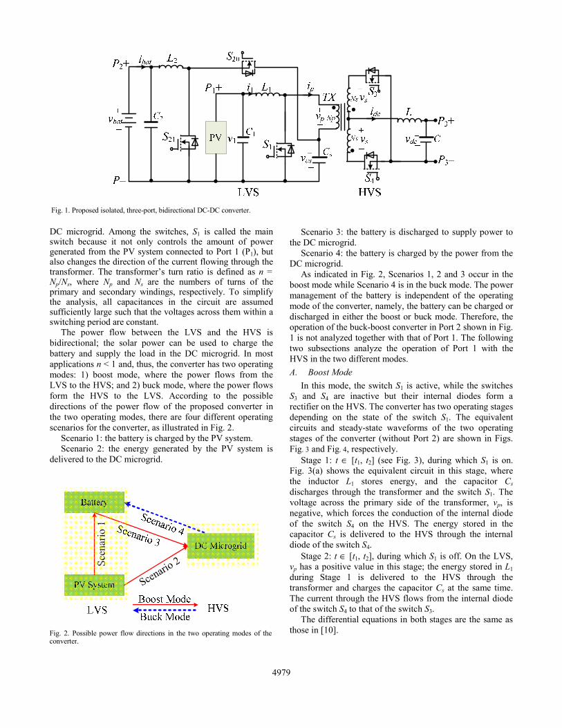
DC microgrid. Among the switches, S1 is called the main switch because it not only controls the amount of power generated from the PV system connected to Port 1 (P1), but also changes the direction of the current flowing through the transformer. The transformer’s turn ratio is defined as n = Np/Ns, where Np and Ns are the numbers of turns of the primary and secondary windings, respectively. To simplify the analysis, all capacitances in the circuit are assumed sufficiently large such that the voltages across them within a switching period are constant.
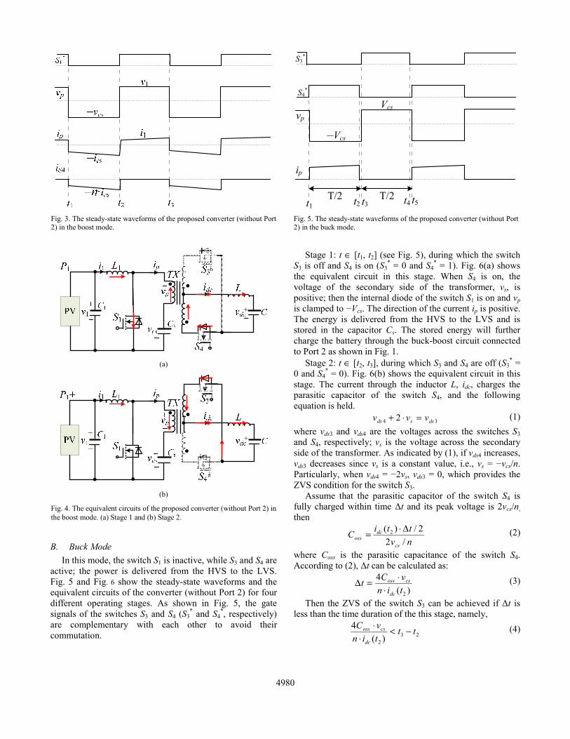
The power flow between the LVS and the HVS is bidirectional; the solar power can be used to charge the battery and supply the load in the DC microgrid. In most applications n < 1 and, thus, the converter has two operating modes: 1) boost mode, where the power flows from the LVS to the HVS; and 2) buck mode, where the power flows form the HVS to the LVS. According to the possible directions of the power flow of the proposed converter in the two operating modes, there are four different operating scenarios for the converter, as illustrated in Fig. 2.
Scenario 1: the battery is charged by the PV system. Scenario 2: the energy generated by the PV system is
delivered to the DC microgrid.
Scenario 3: the battery is discharged to supply power to the DC microgrid.
Scenario 4: the battery is charged by the power from the DC microgrid.
As indicated in Fig. 2, Scenarios 1, 2 and 3 occur in the boost mode while Scenario 4 is in the buck mode. The power management of the battery is independent of the operating mode of the converter, namely, the battery can be charged or discharged in either the boost or buck mode. Therefore, the operation of the buck-boost converter in Port 2 shown in Fig. 1 is not analyzed together with that of Port 1. The following two subsections analyze the operation of Port 1 with the HVS in the two different modes. A. Boost Mode
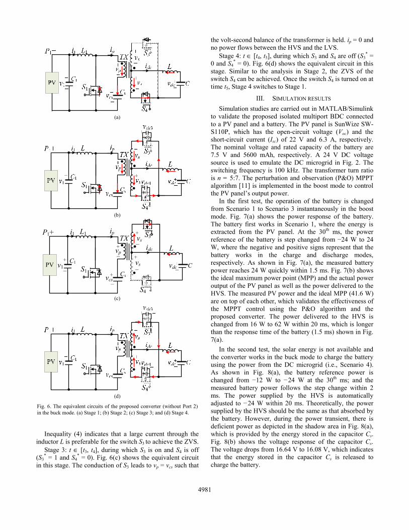
In this mode, the switch S1 is active, while the switches S3 and S4 are inactive but their internal diodes form a rectifier on the HVS. The converter has two operating stages depending on the state of the switch S1. The equivalent circuits and steady-state waveforms of the two operating stages of the converter (without Port 2) are shown in Figs. Fig. 3 and Fig. 4, respectively.
Stage 1: t ∈ [t1, t2] (see Fig. 3), during which S1 is on. Fig. 3(a) shows the equivalent circuit in this stage, where the inductor L1 stores energy, and the capacitor Cs discharges through the transformer and the switch S1. The voltage across the primary side of the transformer, vp, is negative, which forces the conduction of the internal diode of the switch S4 on the HVS. The energy stored in the capacitor Cs is delivered to the HVS through the internal diode of the switch S4.
Stage 2: t ∈ [t1, t2], during which S1 is off. On the LVS, vp has a positive value in this stage; the energy stored in L1 during Stage 1 is delivered to the HVS through the transformer and charges the capacitor Cs at the same time. The current through the HVS flows from the internal diode of the switch S4 to that of the switch S3.
The differential equations in both stages are the same as those in [10].
Fig. 1. Proposed isolated, three-port, bidirectional DC-DC converter.
Fig. 2. Possible power flow directions in the two operating modes of the converter.
Scen
ario
1
Scenario 2
4979
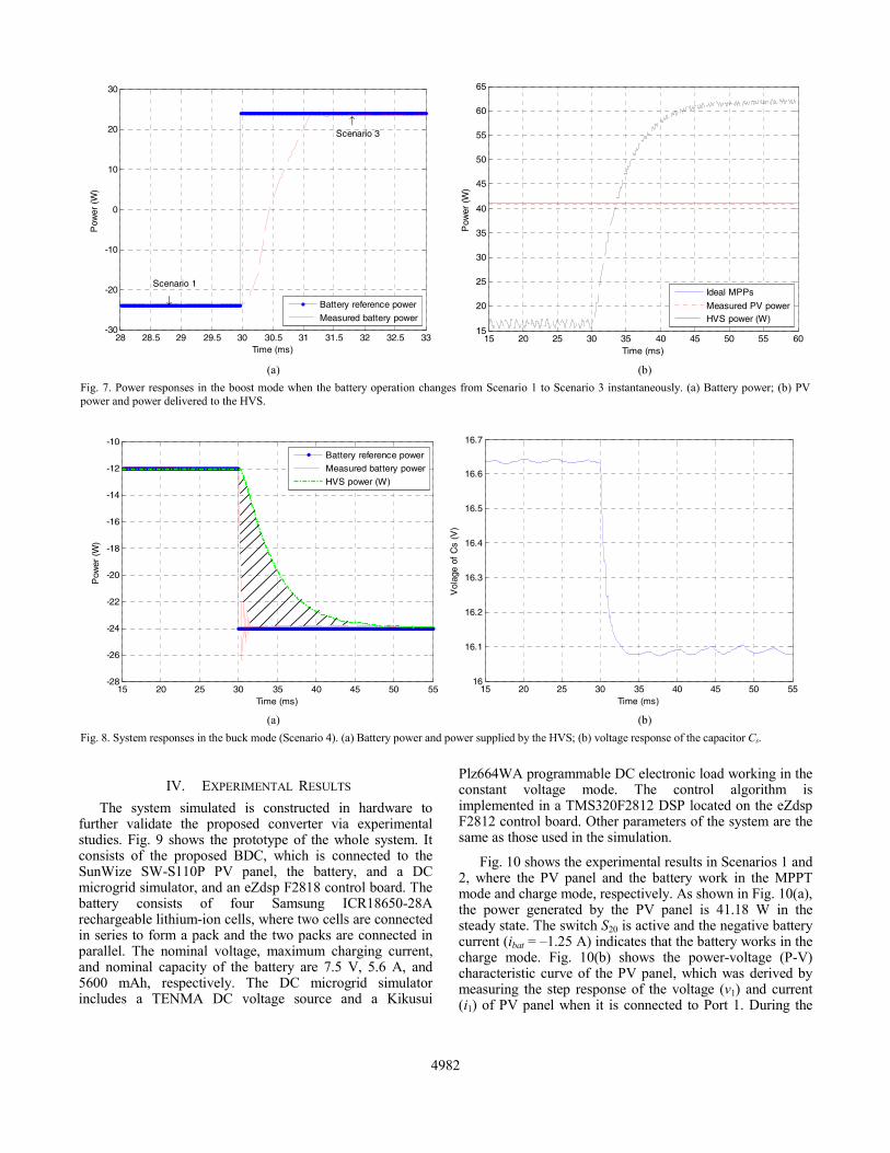
B. Buck Mode In this mode, the switch S1 is inactive, while S3 and S4 are
active; the power is delivered from the HVS to the LVS. Fig. 5 and Fig. 6 show the steady-state waveforms and the equivalent circuits of the converter (without Port 2) for four different operating stages. As shown in Fig. 5, the gate signals of the switches S3 and S4 (S3
* and S4*, respectively)
are complementary with each other to avoid their commutation.
Stage 1: t ∈ [t1, t2] (see Fig. 5), during which the switch S3 is off and S4 is on (S3
* = 0 and S4* = 1). Fig. 6(a) shows
the equivalent circuit in this stage. When S4 is on, the voltage of the secondary side of the transformer, vs, is positive; then the internal diode of the switch S1 is on and vp is clamped to −Vcs. The direction of the current ip is positive. The energy is delivered from the HVS to the LVS and is stored in the capacitor Cs. The stored energy will further charge the battery through the buck-boost circuit connected to Port 2 as shown in Fig. 1.
Stage 2: t ∈ [t2, t3], during which S3 and S4 are off (S3* =
0 and S4* = 0). Fig. 6(b) shows the equivalent circuit in this
stage. The current through the inductor L, idc, charges the parasitic capacitor of the switch S4, and the following equation is held.
34 2 dssds vvv =⋅+ (1) where vds3 and vds4 are the voltages across the switches S3 and S4, respectively; vs is the voltage across the secondary side of the transformer. As indicated by (1), if vds4 increases, vds3 decreases since vs is a constant value, i.e., vs = −vcs/n. Particularly, when vds4 = −2vs, vds3 = 0, which provides the ZVS condition for the switch S3.
Assume that the parasitic capacitor of the switch S4 is fully charged within time Δt and its peak voltage is 2vcs/n, then
nvttiC
cs
dcoss /2
2/)( 2 Δ⋅= (2)
where Coss is the parasitic capacitance of the switch S4. According to (2), Δt can be calculated as:
)(4
2tinvCt
dc
csoss
⋅⋅=Δ (3)
Then the ZVS of the switch S3 can be achieved if Δt is less than the time duration of the this stage, namely,
232 )(
4 tttinvC
dc
csoss −<⋅
⋅ (4)
Fig. 3. The steady-state waveforms of the proposed converter (without Port 2) in the boost mode.
(a)
(b)
Fig. 4. The equivalent circuits of the proposed converter (without Port 2) in the boost mode. (a) Stage 1 and (b) Stage 2.
Fig. 5. The steady-state waveforms of the proposed converter (without Port 2) in the buck mode.
++
t1 t2 t3
vp
–Vcs
Vcs
S3*
S4*
ip
T/2 T/2 t4 t5
4980
Inequality (4) indicates that a large current through the inductor L is preferable for the switch S3 to achieve the ZVS.
Stage 3: t ∈ [t3, t4], during which S3 is on and S4 is off (S3
* = 1 and S4* = 0). Fig. 6(c) shows the equivalent circuit
in this stage. The conduction of S3 leads to vp = vcs such that
the volt-second balance of the transformer is held. ip = 0 and no power flows between the HVS and the LVS.
Stage 4: t ∈ [t4, t5], during which S3 and S4 are off (S3* =
0 and S4* = 0). Fig. 6(d) shows the equivalent circuit in this
stage. Similar to the analysis in Stage 2, the ZVS of the switch S4 can be achieved. Once the switch S4 is turned on at time t5, Stage 4 switches to Stage 1.
III. SIMULATION RESULTS Simulation studies are carried out in MATLAB/Simulink
to validate the proposed isolated multiport BDC connected to a PV panel and a battery. The PV panel is SunWize SW-S110P, which has the open-circuit voltage (Voc) and the short-circuit current (Isc) of 22 V and 6.3 A, respectively. The nominal voltage and rated capacity of the battery are 7.5 V and 5600 mAh, respectively. A 24 V DC voltage source is used to emulate the DC microgrid in Fig. 2. The switching frequency is 100 kHz. The transformer turn ratio is n = 5:7. The perturbation and observation (P&O) MPPT algorithm [11] is implemented in the boost mode to control the PV panel’s output power.
In the first test, the operation of the battery is changed from Scenario 1 to Scenario 3 instantaneously in the boost mode. Fig. 7(a) shows the power response of the battery. The battery first works in Scenario 1, where the energy is extracted from the PV panel. At the 30th ms, the power reference of the battery is step changed from −24 W to 24 W, where the negative and positive signs represent that the battery works in the charge and discharge modes, respectively. As shown in Fig. 7(a), the measured battery power reaches 24 W quickly within 1.5 ms. Fig. 7(b) shows the ideal maximum power point (MPP) and the actual power output of the PV panel as well as the power delivered to the HVS. The measured PV power and the ideal MPP (41.6 W) are on top of each other, which validates the effectiveness of the MPPT control using the P&O algorithm and the proposed converter. The power delivered to the HVS is changed from 16 W to 62 W within 20 ms, which is longer than the response time of the battery (1.5 ms) shown in Fig. 7(a).
In the second test, the solar energy is not available and the converter works in the buck mode to charge the battery using the power from the DC microgrid (i.e., Scenario 4). As shown in Fig. 8(a), the battery reference power is changed from −12 W to −24 W at the 30th ms; and the measured battery power follows the step change within 2 ms. The power supplied by the HVS is automatically adjusted to −24 W within 20 ms. Theoretically, the power supplied by the HVS should be the same as that absorbed by the battery. However, during the power transient, there is deficient power as depicted in the shadow area in Fig. 8(a), which is provided by the energy stored in the capacitor Cs. Fig. 8(b) shows the voltage response of the capacitor Cs. The voltage drops from 16.64 V to 16.08 V, which indicates that the energy stored in the capacitor Cs is released to charge the battery.
(a)
(b)
(c)
(d)
Fig. 6. The equivalent circuits of the proposed converter (without Port 2) in the buck mode. (a) Stage 1; (b) Stage 2; (c) Stage 3; and (d) Stage 4.
L1
S1
+
–
i1
Cs
+
–vp
ipTX
+
–vcs
v1
P1+
C1PV
S3
S4
– Cvdc
Lidc
+vs–
+vs–
4981
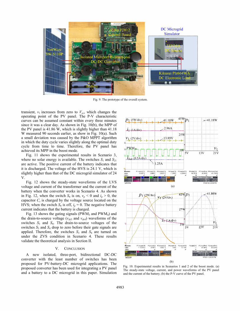
IV. EXPERIMENTAL RESULTS The system simulated is constructed in hardware to
further validate the proposed converter via experimental studies. Fig. 9 shows the prototype of the whole system. It consists of the proposed BDC, which is connected to the SunWize SW-S110P PV panel, the battery, and a DC microgrid simulator, and an eZdsp F2818 control board. The battery consists of four Samsung ICR18650-28A rechargeable lithium-ion cells, where two cells are connected in series to form a pack and the two packs are connected in parallel. The nominal voltage, maximum charging current, and nominal capacity of the battery are 7.5 V, 5.6 A, and 5600 mAh, respectively. The DC microgrid simulator includes a TENMA DC voltage source and a Kikusui
Plz664WA programmable DC electronic load working in the constant voltage mode. The control algorithm is implemented in a TMS320F2812 DSP located on the eZdsp F2812 control board. Other parameters of the system are the same as those used in the simulation.
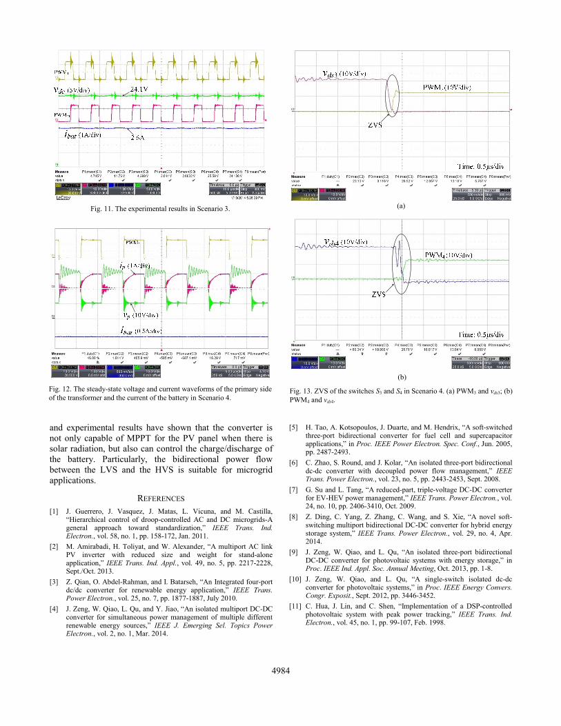
Fig. 10 shows the experimental results in Scenarios 1 and 2, where the PV panel and the battery work in the MPPT mode and charge mode, respectively. As shown in Fig. 10(a), the power generated by the PV panel is 41.18 W in the steady state. The switch S20 is active and the negative battery current (ibat = –1.25 A) indicates that the battery works in the charge mode. Fig. 10(b) shows the power-voltage (P-V) characteristic curve of the PV panel, which was derived by measuring the step response of the voltage (v1) and current (i1) of PV panel when it is connected to Port 1. During the
(a) (b) Fig. 7. Power responses in the boost mode when the battery operation changes from Scenario 1 to Scenario 3 instantaneously. (a) Battery power; (b) PV power and power delivered to the HVS.
(a) (b) Fig. 8. System responses in the buck mode (Scenario 4). (a) Battery power and power supplied by the HVS; (b) voltage response of the capacitor Cs.
28 28.5 29 29.5 30 30.5 31 31.5 32 32.5 33-30
-20
-10
0
10
20
30
Time (ms)
Pow
er (
W)
↓
Scenario 1
↑Scenario 3
Battery reference power
Measured battery power
15 20 25 30 35 40 45 50 55 6015
20
25
30
35
40
45
50
55
60
65
Time (ms)
Pow
er (
W)
Ideal MPPs
Measured PV powerHVS power (W)
15 20 25 30 35 40 45 50 55-28
-26
-24
-22
-20
-18
-16
-14
-12
-10
Time (ms)
Pow
er (
W)
Battery reference power
Measured battery power
HVS power (W)
15 20 25 30 35 40 45 50 5516
16.1
16.2
16.3
16.4
16.5
16.6
16.7
Time (ms)
Vol
age
of C
s (V
)
4982
transient, v1 increases from zero to Voc, which changes the operating point of the PV panel. The P-V characteristic curves can be assumed constant within every three minutes since it was a clear day. As shown in Fig. 10(b), the MPP of the PV panel is 41.86 W, which is slightly higher than 41.18 W measured 90 seconds earlier, as show in Fig. 10(a). Such a small deviation was caused by the P&O MPPT algorithm in which the duty cycle varies slightly along the optimal duty cycle from time to time. Therefore, the PV panel has achieved its MPP in the boost mode.
Fig. 11 shows the experimental results in Scenario 3, where no solar energy is available. The switches S1 and S21 are active. The positive current of the battery indicates that it is discharged. The voltage of the HVS is 24.1 V, which is slightly higher than that of the DC microgrid simulator of 24 V.
Fig. 12 shows the steady-state waveforms of the LVS voltage and current of the transformer and the current of the battery when the converter works in Scenario 4. As shown in Fig. 12, when the switch S4 is on, vp < 0 and ip > 0, the capacitor Cs is charged by the voltage source located on the HVS; when the switch S4 is off, ip = 0. The negative battery current indicates that the battery is charged.
Fig. 13 shows the gating signals (PWM3 and PWM4) and the drain-to-source voltage (vds3 and vds4) waveforms of the switches S3 and S4. The drain-to-source voltages of the switches S3 and S4 drop to zero before their gate signals are applied. Therefore, the switches S3 and S4 are turned on under the ZVS condition in Scenario 4. These results validate the theoretical analysis in Section II.
V. CONCLUSION A new isolated, three-port, bidirectional DC-DC
converter with the least number of switches has been proposed for PV-battery-DC microgrid applications. The proposed converter has been used for integrating a PV panel and a battery to a DC microgrid in this paper. Simulation
Fig. 9. The prototype of the overall system.
(a)
(b)
Fig. 10. Experimental results in Scenarios 1 and 2 of the boost mode. (a) The steady-state voltage, current, and power waveforms of the PV panel and the current of the battery; (b) the P-V curve of the PV panel.
p1
v15V 13V 21V
5W
25W
45Wp1 (5W/div)
v1 (2V/div)
i1 (1A/div)
41.18W
PWM20
2.96A
ibat (0.5A/div)
– 1.25A
41.18W
13.89V
4983
and experimental results have shown that the converter is not only capable of MPPT for the PV panel when there is solar radiation, but also can control the charge/discharge of the battery. Particularly, the bidirectional power flow between the LVS and the HVS is suitable for microgrid applications.
REFERENCES [1] J. Guerrero, J. Vasquez, J. Matas, L. Vicuna, and M. Castilla,
“Hierarchical control of droop-controlled AC and DC microgrids-A general approach toward standardization,” IEEE Trans. Ind. Electron., vol. 58, no. 1, pp. 158-172, Jan. 2011.
[2] M. Amirabadi, H. Toliyat, and W. Alexander, “A multiport AC link PV inverter with reduced size and weight for stand-alone application,” IEEE Trans. Ind. Appl., vol. 49, no. 5, pp. 2217-2228, Sept./Oct. 2013.
[3] Z. Qian, O. Abdel-Rahman, and I. Batarseh, “An Integrated four-port dc/dc converter for renewable energy application,” IEEE Trans. Power Electron., vol. 25, no. 7, pp. 1877-1887, July 2010.
[4] J. Zeng, W. Qiao, L. Qu, and Y. Jiao, “An isolated multiport DC-DC converter for simultaneous power management of multiple different renewable energy sources,” IEEE J. Emerging Sel. Topics Power Electron., vol. 2, no. 1, Mar. 2014.
[5] H. Tao, A. Kotsopoulos, J. Duarte, and M. Hendrix, “A soft-switched three-port bidirectional converter for fuel cell and supercapacitor applications,” in Proc. IEEE Power Electron. Spec. Conf., Jun. 2005, pp. 2487-2493.
[6] C. Zhao, S. Round, and J. Kolar, “An isolated three-port bidirectional dc-dc converter with decoupled power flow management,” IEEE Trans. Power Electron., vol. 23, no. 5, pp. 2443-2453, Sept. 2008.
[7] G. Su and L. Tang, “A reduced-part, triple-voltage DC-DC converter for EV-HEV power management,” IEEE Trans. Power Electron., vol. 24, no. 10, pp. 2406-3410, Oct. 2009.
[8] Z. Ding, C. Yang, Z. Zhang, C. Wang, and S. Xie, “A novel soft-switching multiport bidirectional DC-DC converter for hybrid energy storage system,” IEEE Trans. Power Electron., vol. 29, no. 4, Apr. 2014.
[9] J. Zeng, W. Qiao, and L. Qu, “An isolated three-port bidirectional DC-DC converter for photovoltaic systems with energy storage,” in Proc. IEEE Ind. Appl. Soc. Annual Meeting, Oct. 2013, pp. 1-8.
[10] J. Zeng, W. Qiao, and L. Qu, “A single-switch isolated dc-dc converter for photovoltaic systems,” in Proc. IEEE Energy Convers. Congr. Exposit., Sept. 2012, pp. 3446-3452.
[11] C. Hua, J. Lin, and C. Shen, “Implementation of a DSP-controlled photovoltaic system with peak power tracking,” IEEE Trans. Ind. Electron., vol. 45, no. 1, pp. 99-107, Feb. 1998.
Fig. 11. The experimental results in Scenario 3.
Fig. 12. The steady-state voltage and current waveforms of the primary side of the transformer and the current of the battery in Scenario 4.
(a)
(b)
Fig. 13. ZVS of the switches S3 and S4 in Scenario 4. (a) PWM3 and vds3; (b) PWM4 and vds4.
4984


![Implementation of SEPIC/Zeta Three-Port Bidirectional DC ...vanished by introducing the multiport dc-dc converter [5-6]. These multi-port dc-dc converters can interface several number](https://img.pdfslide.net/doc/110x75/5f3cc4b88e446c087f3c5e0b/implementation-of-sepiczeta-three-port-bidirectional-dc-vanished-by-introducing.jpg)


![A Switched-Capacitor Bidirectional DC-DC Converter with ...download.xuebalib.com/j7vm5PpVeSl.pdf · inductance, a bidirectional DC-DC converter with an active clamp circuit in [12]](https://img.pdfslide.net/doc/110x75/5b5053ee7f8b9a2a6e8e29da/a-switched-capacitor-bidirectional-dc-dc-converter-with-inductance-a-bidirectional.jpg)