Embed Size (px)
Citation preview

AN11623 LPC82x Touch Solution Hardware Design Guide Rev. 1.0 — 22 December 2014 Application Note
Document information Info Content Keywords Capacitive Touch, Touchpad, Sensor, Electrode, Drive/Sensing lines,
Dielectric, Overlay panel, Sensitivity, Touch, False Touch.
Abstract This application note describes the overall hardware design aspect of NXP’s Capacitive Touch solution, shows the schematic design, materials, and PCB design including the most critical Touch sensor design.

NXP Semiconductors AN11623 LPC82x Touch Solution Hardware Design Guide
AN11623 All information provided in this document is subject to legal disclaimers. © NXP B.V. 2014. All rights reserved.
Application Note Rev. 1.0 — 22 December 2014 2 of 18
Contact information For more information, please visit: http://www.nxp.com For sales office addresses, please send an email to: [email protected]
Revision history Rev Date Description 1.0 20141222 Initial version

NXP Semiconductors AN11623 LPC82x Touch Solution Hardware Design Guide
AN11623 All information provided in this document is subject to legal disclaimers. © NXP B.V. 2014. All rights reserved.
Application Note Rev. 1.00 — 22 December 2014 3 of 18
1. Introduction Appropriate hardware design is critical to a robust implementation of capacitive Touch detection. The key is to achieve optimum signal-to-noise ratio, ideally more the better. To achieve optimum performance, a lot of factors have to be considered, resulting in multiple design iterations. However, one can easily reduce the number of design iterations by knowing the pros and cons upfront or following some of the best design practices. This application note describes the overall hardware design aspect of NXP’s Capacitive Touch solution, technology overview, the schematic design, the PCB design, the materials, and finally, the most critical Touch sensor design.
1.1 Overview A capacitor is a passive two terminal electrical component used to store the energy in an electric field. It has a large uniform field and a small fringe field which helps to get a deterministic performance without any external influence.
In capacitive Touch sensing, the ultimate goal is to detect a Touch using relative change in the capacitance of capacitive Touch sensor that calls for an external influence.
A good capacitive Touch sensor is basically a capacitor having a small uniform field and a large fringe field, resulting in a high external influence on the capacitance. See Fig-1.
Fig 1. Touch Sensor
The maximal inter-leaving of X and Y electrodes in T sensor forms a capacitor Cx. When a DC voltage is applied between the X-electrode (driving electrode) and the Y-electrode (receiving electrode) a charge current flows until sensor capacitor Cx is fully charged. The amount of charge flowing into sensor capacitor Cx depends on its capacitance and the applied voltage.

NXP Semiconductors AN11623 LPC82x Touch Solution Hardware Design Guide
AN11623 All information provided in this document is subject to legal disclaimers. © NXP B.V. 2014. All rights reserved.
Application Note Rev. 1.00 — 22 December 2014 4 of 18
The fringe field lines of the capacitor Cx arc through the dielectric overlay material. With a Touch in a grounded system the human finger distracts some of the charge during a charging condition. See Fig-2. As a result, the sensor capacitance Cx is effectively reduced (Cx-∆Cx).
Fig 2. Touch Sensing (Grounded System)
While in the groundless system (see Fig-3), the human finger adds up (+∆Cx) to the sensor capacitance Cx and the effective capacitance is increased (Cx+∆Cx).

NXP Semiconductors AN11623 LPC82x Touch Solution Hardware Design Guide
AN11623 All information provided in this document is subject to legal disclaimers. © NXP B.V. 2014. All rights reserved.
Application Note Rev. 1.00 — 22 December 2014 5 of 18
Fig 3. Touch Sensing (Groundless System)
This very small relative change (-∆Cx or +∆Cx) in the sensor capacitance is detected as a Touch. In addition, there’s a lot of post processing involved to increase the robustness, to filter out the noise/jitter, to control the sensitivity, and to compensate for the environmental changes, such as, change in humidity, temperature, or operating voltage.
NXP Semiconductors AN11623 LPC82x Touch Solution Hardware Design Guide
AN11623 All information provided in this document is subject to legal disclaimers. © NXP B.V. 2014. All rights reserved.
Application Note Rev. 1.00 — 22 December 2014 6 of 18
2. Schematic Design
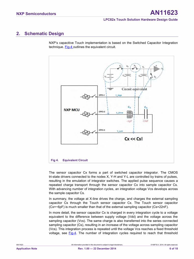
NXP’s capacitive Touch implementation is based on the Switched Capacitor Integration technique. Fig-4 outlines the equivalent circuit.
Fig 4. Equivalent Circuit
The sensor capacitor Cx forms a part of switched capacitor integrator. The CMOS tri-state drivers connected to the nodes X, Y-H and Y-L are controlled by trains of pulses, resulting in the emulation of integrator switches. The applied pulse sequence causes a repeated charge transport through the sensor capacitor Cx into sample capacitor Cs. With advancing number of integration cycles, an integration voltage Vcs develops across the sample capacitor Cs.
In summary, the voltage at X-line drives the charge, and charges the external sampling capacitor Cs through the Touch sensor capacitor Cx. The Touch sensor capacitor (Cx=~6pF) is much smaller than that of the external sampling capacitor (Cs=22nF).
In more detail, the sensor capacitor Cx is charged in every integration cycle to a voltage equivalent to the difference between supply voltage (Vdd) and the voltage across the sampling capacitor (Vcs). The same charge is also transferred into the series connected sampling capacitor (Cs), resulting in an increase of the voltage across sampling capacitor (Vcs). This integration process is repeated until the voltage Vcs reaches a fixed threshold voltage, see Fig-4. The number of integration cycles required to reach that threshold

NXP Semiconductors AN11623 LPC82x Touch Solution Hardware Design Guide
AN11623 All information provided in this document is subject to legal disclaimers. © NXP B.V. 2014. All rights reserved.
Application Note Rev. 1.00 — 22 December 2014 7 of 18
voltage is a measure for the capacitance of sensor capacitor Cx. The integration cycle count performed with no-touch is the reference and forms the basis for Touch detection.
Fig 5. Switched Capacitor Integration Process
With a finger touch, the effective sensor capacitance (Cx-ΔCx) is reduced as the finger distracts some charge. Hence, it takes more integration cycles until the voltage across Cs reaches the threshold voltage. And that is the indication of a Touch. After the Touch has been detected, further filtering and processing techniques are deployed to ensure the validity of Touch. The sensitivity of the Touch sensor is determined by the threshold voltage (Vth) as well as the capTouchacitance of the sample capacitor Cs.
2.1 Clean Supply (Vdd) Special care must be taken while deriving the supply (Vdd) for Touch application. A dedicated voltage regulator (LDO) is always preferred. In case the voltage regulator is shared with other circuitry, proper filtering is recommended in supply path to isolate/filter noise from other circuitry getting into Touch sensing. The maximum ripple in supply should not exceed 20mV peak-to-peak.
2.2 X (Drive) Lines No special consideration is needed while selecting the drive (X) lines. GPIO pins used should be able to switch between High Impedance, Input & Output (High/Low) and shall preferably have low pad/stray capacitance.
The series resistors (Rs) on all the X lines can come in handy to increase the conducted immunity in noisy environments. While experiencing noise issues, one can try with the series termination resistors of 1k Ohm.

NXP Semiconductors AN11623 LPC82x Touch Solution Hardware Design Guide
AN11623 All information provided in this document is subject to legal disclaimers. © NXP B.V. 2014. All rights reserved.
Application Note Rev. 1.00 — 22 December 2014 8 of 18
2.3 Y (Sense) Lines These GPIO pins should be able to switch between High Impedance, Input and Output (High/Low) and shall preferably have low pad/stray capacitance. Selecting the proper sense (Y) line pins, especially Y-H pins is very critical to achieve good sensitivity levels on Touch sensors. One must ensure that these sense pins are not multi-function or heavily multiplexed.
The multi-function pins usually will have more stray (parasitic) capacitance which can cause increased loading and hence poor sensitivity.
We should not even add any external circuit on these lines which could in turn affect the sensitivity. In particular, switching LEDs can cause the Touch measurement to be much really noisy.
2.4 Sampling Capacitor (Cs) Sampling capacitor (Cs) is the only critical external component in the circuit. And since Cs decides the overall Touch sensitivity, stability of this capacitor is important in achieving a consistent and repeatable measurement. A capacitor with X7R dielectric or better has a low temperature co-efficient and will be more stable.
2.5 LEDs The changing capacitance from switching LEDs can cause detection instability and stuck-on state in nearby sensors. This is particularly true if LEDs are pulled down or up to switch on, but are allowed to float when off. If such LEDs are less than 4mm away from capacitive sensors, they must be bypassed with a small capacitor that has a typical value of 1nF. Mounting LEDs or having lighting guides in between the sensors is not recommended in touchpad applications.
2.6 Ground Pins When sensor (touchpad) board is isolated from Touch MCU board, prefer using multiple ground pins in the connectors for effective return path.

NXP Semiconductors AN11623 LPC82x Touch Solution Hardware Design Guide
AN11623 All information provided in this document is subject to legal disclaimers. © NXP B.V. 2014. All rights reserved.
Application Note Rev. 1.00 — 22 December 2014 9 of 18
3. PCB Design
3.1 PCB Material The capacitive Touch circuits or sensors are usually constructed on printed circuit boards. And the most commonly used PCBs are FR4. Whenever the end products/applications demand flexibility and/or transparency, flexible PCBs are generally preferred. The ITO (Indium Tin Oxide) is also commonly used with silver ink to lay the sensors and traces wherever transparency (look and feel) is more important.
3.2 Sensing Components The sensing components, like sampling capacitor (Cs) and series resistor (Rs) should be placed close to the Microcontroller pins to get the best results.
3.3 Sensor Placements The sensors should be placed on the layer closest to the Touch in order to maximize the sensitivity. One should not place the MCU or any other components directly under the sensor or even in the proximity. The Touch sensors (touchpad) should be placed away and well isolated from other circuitry to avoid any sort of noise affecting the Touch measurements. Preferably, no other circuit connections should pass through sensing (touchpad) area even on a different layer in the PCB stack-up.
3.4 Sensing (Y) Lines Special care must be taken while routing the sense (Y) lines, especially Y-H lines. These lines being very sensitive analog sensing lines must be thin (0.1mm to 0.5mm) and routed as short as possible. Having long traces will be more prone to external noise and loading from nearby circuit. Also, to prevent false touches, it is always preferred to keep these traces thin and short. Normally, these Electrodes drive very small loads (in few pF), therefore, minimum trace widths are just sufficient. The sense tracks, being sensitive to touch, must be routed through the bottom layer of the two-layer PCB. This prevents false detections on the Touch surface. One must also avoid VIAs on these sense lines to avoid any pick-up from the external world.
The GND tracks should not be placed near the sense lines. They will have loading effect which will reduce the overall sensitivity of Touch sensors. If it cannot be avoided, one must ensure that the sense lines are separated from GND tracks by at least T/2, where T is overlay panel thickness. To reduce loading, the sense lines and GND track should cross at 90° on separate layers. As a rule of thumb, the sense lines should not be placed near other tracks and components, as this may cause loading and/or interference. The tracks with switching signals can inject noise in the sense lines if they are placed too close. Again, the minimum separation between the sense lines and all other tracks or components should be at least T/2, where T is overlay panel thickness.
3.5 Drive (X) Lines Avoid close parallel X lines, otherwise, you might experience crosstalk effects like “ghost” touches. In this case, driving one sensor easily induces charge onto the other one. So, if

NXP Semiconductors AN11623 LPC82x Touch Solution Hardware Design Guide
AN11623 All information provided in this document is subject to legal disclaimers. © NXP B.V. 2014. All rights reserved.
Application Note Rev. 1.00 — 22 December 2014 10 of 18
you are touching on one sensor you will receive the signal on another sensor too. The safe distance between the X lines should be >3*width of X line to avoid any crosstalk.
3.6 No (close) parallel X and Y Lines The drive (X) and sensing (Y) lines should be well separated or isolated from each other.
Strictly avoid running (close) parallel X and Y lines, this will form false (un-intended) Touch areas. And the actual sensors (touchpad) might be adversely affected on sensitivity. If at all X and Y lines have to cross, they must cross perpendicular in order to avoid noise coupling. It’s a good practice to route X and Y lines on different layers if the PCB is multi-layer, similar to the reference design shown in last section.
Fig 6. False Touch
3.7 No (close) switching signals Any clock, data or periodic switching signals should not be routed side by side to the sensor (X or Y) signal traces or sensors. As much as possible, route them far away from the sensor lines or sensors. If at all these other signal traces should cross the sensor lines, they must cross perpendicular to them to avoid any noise coupling.
3.8 Ground near Sensor Ground plane or traces near the sensors or sensing lines will decrease the sensitivity due to loading effect, but at the same time increases the noise immunity. So, it is always a trade-off between the Touch performance (higher sensitivity) and the noise immunity. If the noise immunity is not a major concern, one must avoid GND nearby. If the application demands for greater noise immunity, there must be optimal separation between the sensor or sensing lines and GND traces or planes. As a rule of thumb, this separation should be greater than the overlay dielectric panel thickness. On similar lines, if GND plane is desired for greater noise immunity, it is preferred to use hatched (mesh) ground instead of solid plane.

NXP Semiconductors AN11623 LPC82x Touch Solution Hardware Design Guide
AN11623 All information provided in this document is subject to legal disclaimers. © NXP B.V. 2014. All rights reserved.
Application Note Rev. 1.00 — 22 December 2014 11 of 18
4. Materials
4.1 Overlay The characteristics of an overlay (front panel) material between the touching object (typically a finger) and actual sensor majorly affects the Touch performance. And the deciding factor is relative permittivity ( ), which is a measure of how well the material propagates an electric field. Higher the relative permittivity, better the propagation.
The same can be easily illustrated by simple parallel plate capacitance expression.
A/T C
Where,
Dielectric constant ( ) = 0 r
0 = Free space permittivity
r = Relative permittivity of the overlay panel/material
A = Area of the touched region (in square meters), and
T = Thickness of the overlay panel/material
So, the thinner overlay panels with higher relative permittivity material yields higher capacitance change during Touch and hence a higher signal and a better sensitivity. Table 1 shows some common overlay materials and their relative permittivity for reference.
Table 1. Relative permittivity of some overlay materials
Materials Relative Permittivity ( r ) ABS 2.0 to 2.35
Polypropylene 2.2 to 2.36
Rubber 3
Plexiglas 3.4
FR-4 (Glass fiber + Epoxy) 4.2
Mica 4 to 8
Glass 3.7 to 10
Silicon 11 to 12
Air gaps in any form should be strictly avoided in the overlay panel stack ups. The overlay panel/s must be glued with 3M adhesive transfer tapes or similar material.
4.2 Substrates The substrate is a base material on which the Touch sensors/electrodes are laid out. Generally, any insulating material with low-loss can be a good substrate. Commonly used substrates are PCB materials (FR-4, CEM-1, Polyamide, or Kapton), acrylics, and Glass. The materials whose relative permittivity ( r ) changes with enivronmental changes should be strictly avoided.

NXP Semiconductors AN11623 LPC82x Touch Solution Hardware Design Guide
AN11623 All information provided in this document is subject to legal disclaimers. © NXP B.V. 2014. All rights reserved.
Application Note Rev. 1.00 — 22 December 2014 12 of 18
5. Sensor Design
Designing good Touch sensors is very critical to achieve optimum Signal-to-Noise ratio which depicts the performance in capacitive Touch applications. A good Touch sensor should have a large fringe field resulting in a high external influence on the capacitance.
5.1 Sensor Layout In a sensor, the Y-Electrode is completely surrounded by the X-Electrode. Hence, the electric field only exists in the gap between X-Electrode and Y-Electrode. Surrounding the Y-Electrode with X-Electrode also keeps the field contained and touch sensitive area can be precisely defined. It’s always preferred to have maximum inter-leaving of X and Y electrodes to achieve the optimum Signal-to-Noise ratio, more the better.
The Y-Electrode should be formed with the thinnest trace possible to minimize the noise coupling during the Touch, while thicker X-Electrodes are much better as they maximize the fringe field as well shields the Y-Electrode.
Fig 7. Sensor Layout
The spacing between X and Y electrodes needs to be at least half the overlay panel thickness. If the overlay panel thickness is T, then the X-Y gap should be at least T/2. There should be no other tracks running below the X-Y gap as this can desensitize the sensor.

NXP Semiconductors AN11623 LPC82x Touch Solution Hardware Design Guide
AN11623 All information provided in this document is subject to legal disclaimers. © NXP B.V. 2014. All rights reserved.
Application Note Rev. 1.00 — 22 December 2014 13 of 18
Fig 8. X – Y Separation
An ideal sensor size is slightly larger than a normal finger. It is recommended to have a sensor size that is slightly larger than the item to be sensed (typically a finger). In general larger keys are more sensitive, but avoid oversized keys as they may have a proximity effect. And undersized keys would result in smaller fringe field in-turn the poor sensitivity. Area of contact from a normal sized finger is about 8mm to 10mm in diameter.
Fig 9. Typical Sensor - Size
5.2 Sensor Shapes A very typical and most commonly deployed capacitive Touch sensor with large fringe field, resulting in a high external influence on the capacitance is shown in Fig 5.
But any other shapes with maximum inter-leaving of X and Y electrodes should yield similar results and hence can be easily deployed. So, there is no limitation to one’s artistic thinking while constructing various types/shapes of sensors.

NXP Semiconductors AN11623 LPC82x Touch Solution Hardware Design Guide
AN11623 All information provided in this document is subject to legal disclaimers. © NXP B.V. 2014. All rights reserved.
Application Note Rev. 1.00 — 22 December 2014 14 of 18
5.3 Sensor Dimensions The sensor must be designed for large fringe field (maximal inter-leaving or maximum X/Y fingers). And X trace on the borders should be thicker to ensure that the fields are contained as well Touch sensitive area is precisely defined.
The Y-Electrode should be formed with the thinnest trace possible (0.1mm to 0.5mm) to minimize the possibility of noise coupling during the Touch. Typically, the thickness of X-Electrode traces should be half (T/2) of the overlay panel thickness (T). Given the width of X and Y traces, we must calculate the number of X fingers those will fit in sensor area allowing for the relatively thicker border (at least T wide).
Where,
W = Width of the Sensor
T = Thickness of overlay panel, and
Y width = Y trace width
Any remaining width after considering the number of X fingers must be added to the X border, so the width of X border must also be re-calculated.
See the typical example calculations below to get better understanding on dimensions.
W = 9000um (9.0 mm)
T = 500um (0.5m)
Y-width = 100um (0.1mm)
Given the above, we can calculate the number of X fingers using equation (1), as below.
)1.075.0/()1.05.10.9( Xfingers
85.0/4.7Xfingers
7.8Xfingers
Truncating it, gives us 8Xfingers
2/))1.075.0(81.05.00.9( Xborder
2/)8.64.8( Xborder
mmXborder 8.0
The result is a typical sensor shown in Fig-10 with all the dimensions outlined.
)5.1/()3( YwidthTYwidthTWXfingers (1)
2/))5.1(( YwidthTXfingersYwidthTWXborder (2)

NXP Semiconductors AN11623 LPC82x Touch Solution Hardware Design Guide
AN11623 All information provided in this document is subject to legal disclaimers. © NXP B.V. 2014. All rights reserved.
Application Note Rev. 1.00 — 22 December 2014 15 of 18
Fig 10. Typical Sensor - Dimensions
One can also use the NXP Touchpad Calculator (xls) to calculate all the sensor and touchpad dimensions.
5.4 Separation between Sensors Avoid large gaps or separation in between individual sensors of the touchpad. It might lead to problems in Touch position calculation. The typical recommended gap is 1.2mm. This is not a concern for the fixed keys/buttons application.
Fig 11. Separation between Sensors

NXP Semiconductors AN11623 LPC82x Touch Solution Hardware Design Guide
AN11623 All information provided in this document is subject to legal disclaimers. © NXP B.V. 2014. All rights reserved.
Application Note Rev. 1.00 — 22 December 2014 16 of 18
6. Reference Design
The LPC82x Touch Solution board shown in Fig-12 can serve as a good reference for designing Touch interface using NXP Microcontrollers.
It very well illustrates on the touchpad layout, sensor design, sensing pin selection, and X/Y line traces. The circuit schematics and PCB design (gerber) files are available along with this hardware design guide.
Fig 12. LPC82x Touch Solution

Error!
Un
kno
wn
do
cum
ent
pro
perty
nam
e.
Error! U
nkn
ow
n d
ocu
men
t pro
perty n
ame.
Error! U
nkn
ow
n d
ocu
men
t pro
perty
nam
e.
NXP Semiconductors AN11623 LPC82x Touch Solution Hardware Design Guide
AN11623 All information provided in this document is subject to legal disclaimers. © NXP B.V. 2014. All rights reserved.
Application Note Rev. 1.0 — 22 December 2014 17 of 18
7. Legal information
7.1 Definitions Draft — The document is a draft version only. The content is still under internal review and subject to formal approval, which may result in modifications or additions. NXP Semiconductors does not give any representations or warranties as to the accuracy or completeness of information included herein and shall have no liability for the consequences of use of such information.
7.2 Disclaimers Limited warranty and liability — Information in this document is believed to be accurate and reliable. However, NXP Semiconductors does not give any representations or warranties, expressed or implied, as to the accuracy or completeness of such information and shall have no liability for the consequences of use of such information.
In no event shall NXP Semiconductors be liable for any indirect, incidental, punitive, special or consequential damages (including - without limitation - lost profits, lost savings, business interruption, costs related to the removal or replacement of any products or rework charges) whether or not such damages are based on tort (including negligence), warranty, breach of contract or any other legal theory.
Notwithstanding any damages that customer might incur for any reason whatsoever, NXP Semiconductors’ aggregate and cumulative liability towards customer for the products described herein shall be limited in accordance with the Terms and conditions of commercial sale of NXP Semiconductors.
Right to make changes — NXP Semiconductors reserves the right to make changes to information published in this document, including without limitation specifications and product descriptions, at any time and without notice. This document supersedes and replaces all information supplied prior to the publication hereof.
Suitability for use — NXP Semiconductors products are not designed, authorized or warranted to be suitable for use in life support, life-critical or safety-critical systems or equipment, nor in applications where failure or malfunction of an NXP Semiconductors product can reasonably be expected to result in personal injury, death or severe property or environmental damage. NXP Semiconductors accepts no liability for inclusion and/or use of NXP Semiconductors products in such equipment or applications and therefore such inclusion and/or use is at the customer’s own risk.
Applications — Applications that are described herein for any of these products are for illustrative purposes only. NXP Semiconductors makes no representation or warranty that such applications will be suitable for the specified use without further testing or modification.
Customers are responsible for the design and operation of their applications and products using NXP Semiconductors products, and NXP Semiconductors accepts no liability for any assistance with applications or
customer product design. It is customer’s sole responsibility to determine whether the NXP Semiconductors product is suitable and fit for the customer’s applications and products planned, as well as for the planned application and use of customer’s third party customer(s). Customers should provide appropriate design and operating safeguards to minimize the risks associated with their applications and products.
NXP Semiconductors does not accept any liability related to any default, damage, costs or problem which is based on any weakness or default in the customer’s applications or products, or the application or use by customer’s third party customer(s). Customer is responsible for doing all necessary testing for the customer’s applications and products using NXP Semiconductors products in order to avoid a default of the applications and the products or of the application or use by customer’s third party customer(s). NXP does not accept any liability in this respect.
Export control — This document as well as the item(s) described herein may be subject to export control regulations. Export might require a prior authorization from competent authorities.
Evaluation products — This product is provided on an “as is” and “with all faults” basis for evaluation purposes only. NXP Semiconductors, its affiliates and their suppliers expressly disclaim all warranties, whether express, implied or statutory, including but not limited to the implied warranties of non-infringement, merchantability and fitness for a particular purpose. The entire risk as to the quality, or arising out of the use or performance, of this product remains with customer.
In no event shall NXP Semiconductors, its affiliates or their suppliers be liable to customer for any special, indirect, consequential, punitive or incidental damages (including without limitation damages for loss of business, business interruption, loss of use, loss of data or information, and the like) arising out the use of or inability to use the product, whether or not based on tort (including negligence), strict liability, breach of contract, breach of warranty or any other theory, even if advised of the possibility of such damages.
Notwithstanding any damages that customer might incur for any reason whatsoever (including without limitation, all damages referenced above and all direct or general damages), the entire liability of NXP Semiconductors, its affiliates and their suppliers and customer’s exclusive remedy for all of the foregoing shall be limited to actual damages incurred by customer based on reasonable reliance up to the greater of the amount actually paid by customer for the product or five dollars (US$5.00). The foregoing limitations, exclusions and disclaimers shall apply to the maximum extent permitted by applicable law, even if any remedy fails of its essential purpose.
7.3 Trademarks Notice: All referenced brands, product names, service names and trademarks are property of their respective owners.

NXP Semiconductors AN11623 LPC82x Touch Solution Hardware Design Guide
Please be aware that important notices concerning this document and the product(s) described herein, have been included in the section 'Legal information'.
© NXP B.V. 2014. All rights reserved.
For more information, visit: http://www.nxp.com For sales office addresses, please send an email to: [email protected]
Date of release: 22 December 2014 Document identifier: AN11623
8. Contents
1. Introduction ......................................................... 3 1.1 Overview ............................................................ 3 2. Schematic Design ............................................... 6 2.1 Clean Supply (Vdd) ............................................ 7 2.2 X (Drive) Lines ................................................... 7 2.3 Y (Sense) Lines .................................................. 8 2.4 Sampling Capacitor (Cs) .................................... 8 2.5 LEDs .................................................................. 8 2.6 Ground Pins ....................................................... 8 3. PCB Design .......................................................... 9 3.1 PCB Material ...................................................... 9 3.2 Sensing Components ......................................... 9 3.3 Sensor Placements ............................................ 9 3.4 Sensing (Y) Lines ............................................... 9 3.5 Drive (X) Lines ................................................... 9 3.6 No (close) parallel X and Y Lines ..................... 10 3.7 No (close) switching signals ............................. 10 3.8 Ground near Sensor ......................................... 10 4. Materials ............................................................. 11 4.1 Overlay ............................................................. 11 4.2 Substrates ........................................................ 11 5. Sensor Design ................................................... 12 5.1 Sensor Layout .................................................. 12 5.2 Sensor Shapes ................................................. 13 5.3 Sensor Dimensions .......................................... 14 5.4 Separation between Sensors ........................... 15 6. Reference Design .............................................. 16 7. Legal information .............................................. 17 7.1 Definitions ........................................................ 17 7.2 Disclaimers....................................................... 17 7.3 Trademarks ...................................................... 17 8. Contents ............................................................. 18