Embed Size (px)
Citation preview

September 2018 AN4649 Rev 7 1/78
1
AN4649Application note
Migrating from STM32F1 Series to STM32L4 Series / STM32L4+ Series microntrollers
Introduction
For designers of the STM32 microcontroller applications, being able to replace easily one microcontroller type by another in the same product family is an important asset. Migrating an application to a different microcontroller is often needed, when product requirements grow, putting extra demands on memory size, or increasing the number of I/Os. The cost reduction objectives may also be an argument to switch to smaller components and shrink the PCB area.
This application note analyzes the steps required to migrate an existing design from STM32F1 Series to STM32L4 Series / STM32L4+ Series. Three aspects that must be considered for the migration are: the hardware, the peripheral and the firmware.
This document lists the full set of features available for STM32F1 Series and the equivalent features on STM32L4 Series / STM32L4+ Series (some products may have less features depending on their part number).
To take the best out of this application note, the user must be familiar with the STM32 microcontrollers documentation available on www.st.com with particular focus on:
• STM32F1 Series reference manuals (RM0008, RM0041)
• STM32F1 Series datasheets
• STM32F1 Series programming manuals (PM0068, PM0075)
• STM32L4 Series reference manuals:
– RM0351 (STM32L4x5xx, STM32L4x6xx)
– RM0394 (STM32L41xxx, STM32L42xxx, STM32L43xxx, STM32L44xxx, STM32L45xxx, STM32L46xxx)
– RM0392 (STM32L471xx)
• STM32L4 Series datasheets
• STM32L4+ Series reference manual (RM0432)
• STM32L4+ Series datasheets.
www.st.com

Contents AN4649
2/78 AN4649 Rev 7
Contents
1 STM32L4 Series / STM32L4+ Series overview . . . . . . . . . . . . . . . . . . . . 6
2 Hardware migration . . . . . . . . . . . . . . . . . . . . . . . . . . . . . . . . . . . . . . . . . . 9
3 Boot mode selection . . . . . . . . . . . . . . . . . . . . . . . . . . . . . . . . . . . . . . . . 18
4 Peripheral migration . . . . . . . . . . . . . . . . . . . . . . . . . . . . . . . . . . . . . . . . 21
4.1 STM32 product cross-compatibility . . . . . . . . . . . . . . . . . . . . . . . . . . . . . 21
4.2 Memory mapping . . . . . . . . . . . . . . . . . . . . . . . . . . . . . . . . . . . . . . . . . . . 25
4.3 Direct memory access controller (DMA) . . . . . . . . . . . . . . . . . . . . . . . . . . 29
4.4 Interrupts . . . . . . . . . . . . . . . . . . . . . . . . . . . . . . . . . . . . . . . . . . . . . . . . . 32
4.5 Reset and clock control (RCC) . . . . . . . . . . . . . . . . . . . . . . . . . . . . . . . . . 37
4.5.1 Performance versus VCORE ranges . . . . . . . . . . . . . . . . . . . . . . . . . . . . 40
4.5.2 Peripheral access configuration . . . . . . . . . . . . . . . . . . . . . . . . . . . . . . . 41
4.5.3 Peripheral clock configuration . . . . . . . . . . . . . . . . . . . . . . . . . . . . . . . . 42
4.6 Power control (PWR ) . . . . . . . . . . . . . . . . . . . . . . . . . . . . . . . . . . . . . . . . 44
4.7 Real-time clock (RTC) . . . . . . . . . . . . . . . . . . . . . . . . . . . . . . . . . . . . . . . 48
4.8 General-purpose I/O interface (GPIO) . . . . . . . . . . . . . . . . . . . . . . . . . . . 48
4.9 Extended interrupts and events controller (EXTI) source selection . . . . . 49
4.10 Flash memory . . . . . . . . . . . . . . . . . . . . . . . . . . . . . . . . . . . . . . . . . . . . . . 49
4.11 Universal synchronous asynchronous receiver transmitter (U(S)ART) . . 53
4.12 Inter-integrated circuit (I2C) interface . . . . . . . . . . . . . . . . . . . . . . . . . . . . 55
4.13 Serial peripheral interface (SPI) / IC to IC sound (I2S) / Serial audio interface (SAI) . . . . . . . . . . . . . . . . . . . . . . . . . . . . . . . . . . . 56
4.14 Cyclic redundancy check calculation unit (CRC) . . . . . . . . . . . . . . . . . . . 60
4.15 Controller area network (bxCAN) . . . . . . . . . . . . . . . . . . . . . . . . . . . . . . . 61
4.16 USB on-the-go full-speed (USB OTG FS) . . . . . . . . . . . . . . . . . . . . . . . . 62
4.17 Flexible static memory controller (FMC/FSMC) . . . . . . . . . . . . . . . . . . . . 65
4.18 Analog-to-digital converters (ADC) . . . . . . . . . . . . . . . . . . . . . . . . . . . . . . 66
4.19 Digital-to analog converter (DAC) . . . . . . . . . . . . . . . . . . . . . . . . . . . . . . 68
5 Software migration . . . . . . . . . . . . . . . . . . . . . . . . . . . . . . . . . . . . . . . . . 70
5.1 References . . . . . . . . . . . . . . . . . . . . . . . . . . . . . . . . . . . . . . . . . . . . . . . . 70

AN4649 Rev 7 3/78
AN4649 Contents
3
5.2 Cortex®-M3 and Cortex®-M4 overview . . . . . . . . . . . . . . . . . . . . . . . . . . 70
5.2.1 STM32 Cortex®-M3 processor and core peripherals . . . . . . . . . . . . . . . 70
5.2.2 STM32 Cortex®-M4 processor and core peripherals . . . . . . . . . . . . . . . 71
5.2.3 Software point of view . . . . . . . . . . . . . . . . . . . . . . . . . . . . . . . . . . . . . . 72
5.3 Cortex mapping overview . . . . . . . . . . . . . . . . . . . . . . . . . . . . . . . . . . . . . 74
6 Revision history . . . . . . . . . . . . . . . . . . . . . . . . . . . . . . . . . . . . . . . . . . . 75

List of tables AN4649
4/78 AN4649 Rev 7
List of tables
Table 1. Packages available on STM32L4 Series and STM32L4+ Series . . . . . . . . . . . . . . . . . . . . . 9Table 2. Pinout differences between STM32F1 Series and
STM32L4 Series / STM32L4+ Series (QFP) . . . . . . . . . . . . . . . . . . . . . . . . . . . . . . . . . . . 13Table 3. Pinout differences between STM32F1 Series and
STM32L4 Series / STM32L4+ Series (BGA) . . . . . . . . . . . . . . . . . . . . . . . . . . . . . . . . . . . 13Table 4. Boot modes for STM32L47xxx/48xxx devices and STM32F1 Series . . . . . . . . . . . . . . . . . 18Table 5. Boot modes for STM32L4+ Series, STM32L49xxx/4Axxx,
STM32L45xxx/46xxx, STM32L43xxx/44xxx and STM32L41xxx/42xxx devices. . . . . . . . . 18Table 6. Bootloader interfaces on STM32F1 and STM32L4 Series / STM32L4+ Series . . . . . . . . . 19Table 7. Peripheral compatibility analysis between STM32F1 Series and
STM32L4 Series / STM32L4+ Series . . . . . . . . . . . . . . . . . . . . . . . . . . . . . . . . . . . . . . . . . 21Table 8. Peripheral address mapping differences between STM32F1 Series and
STM32L4 Series / STM32L4+ Series . . . . . . . . . . . . . . . . . . . . . . . . . . . . . . . . . . . . . . . . . 25Table 9. DMA request differences between STM32F1 Series and
STM32L4 Series / STM32L4+ Series . . . . . . . . . . . . . . . . . . . . . . . . . . . . . . . . . . . . . . . . . 29Table 10. Interrupt vector differences between STM32F1 Series
and STM32L4 Series / STM32L4+ Series . . . . . . . . . . . . . . . . . . . . . . . . . . . . . . . . . . . . . 32Table 11. RCC differences between STM32F1 Series
and STM32L4 Series / STM32L4+ Series . . . . . . . . . . . . . . . . . . . . . . . . . . . . . . . . . . . . . 37Table 12. Performance versus VCORE ranges for STM32L4 Series and STM32L4+ Series . . . . . . 40Table 13. RCC registers used for peripheral access configuration for STM32F1 Series
and STM32L4 Series / STM32L4+ Series . . . . . . . . . . . . . . . . . . . . . . . . . . . . . . . . . . . . . 41Table 14. PWR differences between STM32F1 Series and STM32L4 Series / STM32L4+ Series . . 44Table 15. RTC differences between STM32F1 Series and STM32L4 Series / STM32L4+ Series. . . 48Table 16. EXTI differences between STM32F1 Series and STM32L4 Series / STM32L4+ Series . . 49Table 17. Flash differences between STM32F1 Series and STM32L4 Series / STM32L4+ Series . . 50Table 18. U(S)ART differences between STM32F1 Series
and STM32L4 Series / STM32L4+ Series . . . . . . . . . . . . . . . . . . . . . . . . . . . . . . . . . . . . . 53Table 19. I2C differences between STM32F1 Series and STM32L4 Series / STM32L4+ Series . . . 55Table 20. SPI differences between STM32F1 Series and STM32L4 Series / STM32L4+ Series . . . 56Table 21. I2S/SAI differences between STM32F1 Series
and STM32L4 Series / STM32L4+ Series . . . . . . . . . . . . . . . . . . . . . . . . . . . . . . . . . . . . . 57Table 22. CRC differences between STM32F1 Series and STM32L4 Series / STM32L4+ Series . . 60Table 23. bxCAN differences between STM32F1 Series and STM32L4 Series / STM32L4+ Series. 61Table 24. USB OTG FS differences between STM32F1 Series and
STM32L4 Series/ STM32L4+ Series . . . . . . . . . . . . . . . . . . . . . . . . . . . . . . . . . . . . . . . . . 63Table 25. USB FS differences between STM32F1 Series and STM32L4 Series . . . . . . . . . . . . . . . . 64Table 26. FMC/FSMC differences between STM32F1 Series and
STM32L4 Series / STM32L4+ Series . . . . . . . . . . . . . . . . . . . . . . . . . . . . . . . . . . . . . . . . . 65Table 27. ADC differences between STM32F1 Series and STM32L4 Series / STM32L4+ Series . . 67Table 28. DAC differences between STM32F1 Series and STM32L4 Series / STM32L4+ Series . . 68Table 29. Cortex overview mapping for STM32F1 Series and STM32L4 Series / STM32L4+ Series 74Table 30. Document revision history . . . . . . . . . . . . . . . . . . . . . . . . . . . . . . . . . . . . . . . . . . . . . . . . . 75

AN4649 Rev 7 5/78
AN4649 List of figures
5
List of figures
Figure 1. LFQFP144 compatible board design . . . . . . . . . . . . . . . . . . . . . . . . . . . . . . . . . . . . . . . . . 14Figure 2. LQFP100 compatible board design . . . . . . . . . . . . . . . . . . . . . . . . . . . . . . . . . . . . . . . . . . 15Figure 3. LQFP64 compatible board design . . . . . . . . . . . . . . . . . . . . . . . . . . . . . . . . . . . . . . . . . . . 15Figure 4. LQFP48 compatible board design . . . . . . . . . . . . . . . . . . . . . . . . . . . . . . . . . . . . . . . . . . . 16Figure 5. UFBGA100 compatible board design . . . . . . . . . . . . . . . . . . . . . . . . . . . . . . . . . . . . . . . . . 16Figure 6. BGA64 compatible board design . . . . . . . . . . . . . . . . . . . . . . . . . . . . . . . . . . . . . . . . . . . . 17Figure 7. STM32L4 Series / STM32L4+ Series clock generation for SAI Master mode
(when MCLK is required) . . . . . . . . . . . . . . . . . . . . . . . . . . . . . . . . . . . . . . . . . . . . . . . . . . 60Figure 8. STM32 Cortex®-M3 implementation . . . . . . . . . . . . . . . . . . . . . . . . . . . . . . . . . . . . . . . . . . 71Figure 9. STM32 Cortex®-M4 implementation . . . . . . . . . . . . . . . . . . . . . . . . . . . . . . . . . . . . . . . . . . 72

STM32L4 Series / STM32L4+ Series overview AN4649
6/78 AN4649 Rev 7
1 STM32L4 Series / STM32L4+ Series overview
The STM32L4 Series and STM32L4+ Series have a perfect fit in terms of ultra-low power performance, memory size and peripherals at a cost-effective price.
In particular, STM32L4 Series and STM32L4+ Series microcontrollers enable a higher frequency and a higher performance operation than STM32F1 Series. The STM32L4 Series and STM32L4+ Series products feature an Arm®(a) Cortex®-M4 @ up to 120 MHz versus a Cortex®-M3 @ 32 MHz featured on STM32F1 Series. The STM32L4 Series and STM32L4+ Series also feature an optimized Flash memory access through the adaptive real-time memory accelerator (ART Accelerator™).
The STM32L4 Series and STM32L4+ Series microcontrollers increase the low-power efficiency in dynamic mode (μA/MHz), and reach a very low level of static power-consumption on the various available low-power modes.
The detailed list of available features and packages for each product is available in the respective datasheet.
a. Arm is a registered trademark of Arm Limited (or its subsidiaries) in the US and/or elsewhere.

AN4649 Rev 7 7/78
AN4649 STM32L4 Series / STM32L4+ Series overview
77
STM32L4 Series and STM32L4+ Series include a larger set of peripherals with more advanced features compared to STM32F1 Series, such as:
• Advanced encryption standard (AES) hardware accelerator
• Touch sensing controller (TSC)
• Single-wire protocol interface (SWPMI) (not available on STM32L4+ Series)
• Serial audio interface (SAI)
• Low-power UART (LPUART)
• Infrared interface (IRTIM)
• Low-power timer (LPTIM)
• Liquid crystal display controller (LCD) (not available on STM32L4+ Series)
• Digital filter for sigma delta modulators (DFSDM) (for STM32L4+ Series, STM32L49xxx/4Axxx, STM32L47xxx/48xxx and STM32L45xxx/46xxx)
• Operational amplifiers (OPAMP)
• Comparators (COMP)
• Voltage reference buffer (VREFBUF)
• Quad-SPI interface (QUADSPI) (not available on STM32L4+ Series)
• Flexible memory controller (FMC) (FSMC on STM32F1 Series) (for STM32L4+ Series, STM32L49xxx/4Axxx and STM32L47xxx/48xxx only)
• Firewall (FW)
• Random number generator (RNG)
• Clock recovery system (CRS) for USB (for STM32L4+ Series, STM32L49xxx/4Axxx, STM32L45xxx/46xxx, STM32L43xxx/44xxx and STM32L41xxx/42xxx)
• Hash processor (HASH) (for STM32L4Sxxx and STM32L49xxx/4Axxx)
• Digital camera interface (DCMI) (for STM32L4+ Series and STM32L49xxx/4Axxx)
• Chrom-ART AcceleratorTM controller (DMA2D) (for STM32L4+ Series and STM32L49xxx/4Axxx)
• SRAM1 size is different on the various STM32L4xxxx devices:
– 192 Kbytes for STM32L4+ Series devices
– 256 Kbytes for STM32L49xxx/4Axxx
– 96 Kbytes for STM32L47xxx/48xxx
– 128 Kbytes for STM32L45xxx/46xxx
– 48 Kbytes for STM32L43xxx/44xxx
– 32 Kbytes for STM32L41xxx/44xxx
• Additional SRAM2 with data preservation in Standby mode:
– 64 Kbytes for STM32L4+ Series and STM32L49xxx/4Axxx
– 32 Kbytes for STM32L47xxx/48xxx and STM32L45xxx/46xxx
– 16 Kbytes for STM32L43xxx/44xxx
– 8 Kbytes for STM32L41xxx/42xxx
• Additional SRAM3 for STM32L4+ Series:
– 384 Kbytes

STM32L4 Series / STM32L4+ Series overview AN4649
8/78 AN4649 Rev 7
• Dual bank boot and 8-bit ECC on Flash memory (for STM32L4+ Series, STM32L49xxx/4Axxx and STM32L47xxx/48xxx)
• Optimized power consumption, enriched set of low-power modes and support for external SMPS
STM32L45xxx/46xxx, STM32L43xxx/44xxx and STM32L41xxx/42xxx devices implement an USB FS device only instead of an USB OTG FS. They also implement reduced Flash size (512 Kbytes for STM32L45xxx/46xxx, 256 Kbytes for STM32L43xxx/44xxx and 128 Kbytes for STM32L41xxx/42xxx).
This migration guide is covering only the migration from STM32F1 Series to the STM32L4 Series / STM32L4+ Series. The new features present on STM32L4 Series / STM32L4+ Series but not available on STM32F1 Series are not covered in this document. Refer to the STM32L4 Series and STM32L4+ Series reference manuals and datasheets for an exhaustive picture.

AN4649 Rev 7 9/78
AN4649 Hardware migration
77
2 Hardware migration
Some packages are available in both STM32L4 Series / STM32L4+ Series and STM32F1 Series such as: LQFP48, LQFP100, LQFP144, BGA64 and UFBGA100. The other packages available on STM32F1 Series are not available on STM32L4 Series / STM32L4+ Series.
Note that the WLCSP packages in STM32F1 Series and the ones in STM32L4 Series / STM32L4+ Series are not equivalent. They have different die sizes for each product.
The list of available packages in STM32L4 Series and STM32L4+ Series is given in Table 1.
Table 1. Packages available on STM32L4 Series and STM32L4+ Series
Package(1) STM32L4+ Series
STM32L4 SeriesSize
(mm x mm)
Applicable part numbers
STM32L49xxx/4Axxx
STM32L47xxx/48xxx
STM32L45xxx/46xxx
STM32L43xxx/44xxx
STM32L41xxx/42xxx
UFQFPN32 - - - - X X (5 x 5)
STM32L412xx, STM32L422xx, STM32L431xx, STM32L432xx, STM32L442xx
LQFP32 - - - - - X (5 x 5)STM32L412xx, STM32L422xx
LQFP48 - - - - X X (7 x 7)
STM32L412xx, STM32L422xx, STM32L431xx, STM32L433xx, STM32L443xx
UFQFPN48 - - - X X X (7 x 7)
STM32L412xx, STM32L422xx, STM32L431xx, STM32L433xx, STM32L443xx, STM32L451xx, STM32L452xx, STM32L462xx
WLCSP36 - - - - - X(2.85 x 3.07)
STM32L412xx, STM32L422xx
WLCSP49 - - - - X -(3.141 x 3.127)
STM32L431xx, STM32L433xx, STM32L443xx
WLCSP64 - - - - X -(3.141 x 3.127)
STM32L431xx, STM32L433xx, STM32L443xx

Hardware migration AN4649
10/78 AN4649 Rev 7
LQFP64 - X X X X X (10 x 10)
STM32L412xx, STM32L422xx, STM32L431xx, STM32L433xx, STM32L443xx, STM32L451xx, STM32L452xx, STM32L462xx, STM32L471xx, STM32L475xx, STM32L476xx, STM32L486xx, STM32L496xx, STM32L4A6xx
UFBGA64 - - - X X X (5 x 5)
STM32L412xx, STM32L422xx, STM32L431xx, STM32L433xx, STM32L443xx, STM32L451xx, STM32L452xx, STM32L462xx
WLCSP64 - - - X - -(3.357 x 3.657)
STM32L451xx, STM32L452xx, STM32L462xx
WLCSP72 - - X - - -(4.4084 x 3.7594)
STM32L471xx, STM32L475xx, STM32L476xx, STM32L486xx
WLCSP81 - - X - - -(4.4084 x 3.7594)
STM32L476xx
WLCSP100 - X - - - -(4.618 x 4.142)
STM32L496xx, STM32L4A6xx
Table 1. Packages available on STM32L4 Series and STM32L4+ Series (continued)
Package(1) STM32L4+ Series
STM32L4 SeriesSize
(mm x mm)
Applicable part numbers
STM32L49xxx/4Axxx
STM32L47xxx/48xxx
STM32L45xxx/46xxx
STM32L43xxx/44xxx
STM32L41xxx/42xxx

AN4649 Rev 7 11/78
AN4649 Hardware migration
77
LQFP100 X X X X X - (14 x 14)
STM32L431xx, STM32L433xx, STM32L443xx, STM32L451xx, STM32L452xx, STM32L462xx, STM32L471xx, STM32L475xx, STM32L476xx, STM32L486xx, STM32L496xx, STM32L4A6xx, STM32L4R5xx, STM32L4R9xx, STM32L4S5xx, STM32L4S9xx
UFBGA100 - - X X X - (7 x 7)STM32L431xx, STM32L433xx, STM32L443xx
UFBGA132 X X X - - - (7 x 7)
STM32L471xx, STM32L475xx, STM32L476xx, STM32L486xx, STM32L496xx, STM32L4A6xx, STM32L4R5xx, STM32L4S5xx
UFBGA144 X - - - - - (10 x 10)STM32L4R9xx, STM32L4S9xx
LQFP144 X X X - - - (20 x 20)
STM32L471xx, STM32L475xx, STM32L476xx, STM32L486xx, STM32L496xx, STM32L4A6xx, STM32L4R5xx, STM32L4R9xx, STM32L4S5xx, STM32L4S9xx
Table 1. Packages available on STM32L4 Series and STM32L4+ Series (continued)
Package(1) STM32L4+ Series
STM32L4 SeriesSize
(mm x mm)
Applicable part numbers
STM32L49xxx/4Axxx
STM32L47xxx/48xxx
STM32L45xxx/46xxx
STM32L43xxx/44xxx
STM32L41xxx/42xxx

Hardware migration AN4649
12/78 AN4649 Rev 7
WLCSP144 X - - - - -(5.24 x 5.24)
STM32L4R5xx, STM32L4R7xx, STM32L4R9xx, STM32L4S5xx, STM32L4S7xx, STM32L4S9xx
UFBGA169 X X - - - - (7 x 7)
STM32L496xx, STM32L4A6xx, STM32L4R5xx, STM32L4R9xx, STM32L4S5xx, STM32L4S9xx
1. X = supported.
Table 1. Packages available on STM32L4 Series and STM32L4+ Series (continued)
Package(1) STM32L4+ Series
STM32L4 SeriesSize
(mm x mm)
Applicable part numbers
STM32L49xxx/4Axxx
STM32L47xxx/48xxx
STM32L45xxx/46xxx
STM32L43xxx/44xxx
STM32L41xxx/42xxx

AN4649 Rev 7 13/78
AN4649 Hardware migration
77
Table 2 and Table 3 show the pinout differences for packages available in both series. The other packages in STM32F1 Series are not available for STM32L4 Series / STM32L4+ Series.
The STM32L4 Series / STM32L4+ Series and STM32F1 Series devices share a high level of pin compatibility. Most peripherals share the same pins in the two families. The transition from STM32F1 Series to STM32L4 Series and STM32L4+ Series is simple since only a few pins are different.
Note: STM32L4R9xx/4S9xx are not compatible with STM32L4 Series, for more details, refer to the application note Migration between STM32L476xx/486xx and STM32L4+ Series microcontrollers (AN5017).
Table 2. Pinout differences between STM32F1 Series and STM32L4 Series / STM32L4+ Series (QFP)
STM32F1 Series STM32L4 Series / STM32L4+ Series
QFP48
QFP64
QFP100
QFP144
PinoutQFP48
QFP64
QFP100
QFP144
Pinout
5 5 - - PD0-OSC_IN 5 5 - - PH0-OSC_IN
6 6 - - PD1-OSC_OUT 6 6 - - PH1-OSC_OUT
- - 73 106 NC - - 73 106 VDDUSB(1)
36 48 - - VDD 36 48 - - VDDUSB(1)
- - - 95 VDD - - - 95 VDDIO2(1)
1. VDDUSB and VDDIO2 pins can be connected externally to VDD.
- - - 131 VDD - - - 131 VDDIO2(1)
9 13 - - VDDA - 13 - - VDDA/VREF+
44 60 94 138 BOOT0 44 60 94 138 PH3-BOOT0(2)
2. Only for STM32L4R5xx/S5xx, STM32L49xxx/4Axxx, STM32L45xxx/46xxx, STM32L43xxx/44xxx and STM32L41xxx/42xxx.
Table 3. Pinout differences between STM32F1 Series and STM32L4 Series / STM32L4+ Series (BGA)
STM32F1 Series STM32L4 Series / STM32L4+ Series
TFBGA64 UFBGA100 Pinout UFBGA64 UFBGA100 Pinout
C1 - PD0_OCSC_IN C1 - PH0_OCSC_IN
D1 - PD1_OCSC_OUT D1 - PH1_OCSC_OUT
E5 - VDD E5 - VDDUSB(1)
1. VDDUSB pin can be connected externally to VDD
- C11 NC - C11 VDDUSB(1)
G1 - VREF+ G1 - PC3
H1 - VDDA H1 - VDDA
B4 A4 BOOT0 B4 A4 PH3-BOOT0(2)
2. Only for STM32L49xxx/4Axxx, STM32L45xxx/46xxx and STM32L43xxx/44xxx devices.
Hardware migration AN4649
14/78 AN4649 Rev 7
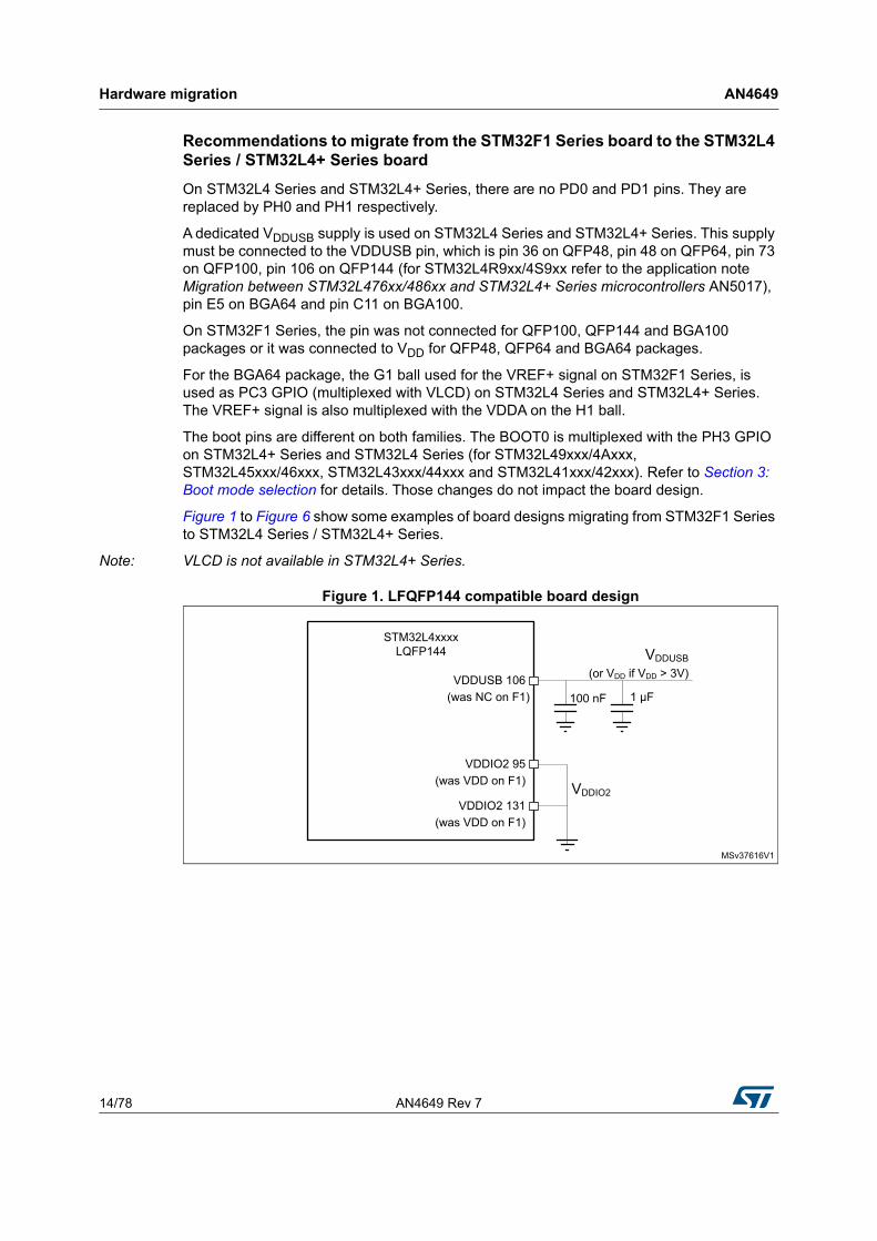
Recommendations to migrate from the STM32F1 Series board to the STM32L4 Series / STM32L4+ Series board
On STM32L4 Series and STM32L4+ Series, there are no PD0 and PD1 pins. They are replaced by PH0 and PH1 respectively.
A dedicated VDDUSB supply is used on STM32L4 Series and STM32L4+ Series. This supply must be connected to the VDDUSB pin, which is pin 36 on QFP48, pin 48 on QFP64, pin 73 on QFP100, pin 106 on QFP144 (for STM32L4R9xx/4S9xx refer to the application note Migration between STM32L476xx/486xx and STM32L4+ Series microcontrollers AN5017), pin E5 on BGA64 and pin C11 on BGA100.
On STM32F1 Series, the pin was not connected for QFP100, QFP144 and BGA100 packages or it was connected to VDD for QFP48, QFP64 and BGA64 packages.
For the BGA64 package, the G1 ball used for the VREF+ signal on STM32F1 Series, is used as PC3 GPIO (multiplexed with VLCD) on STM32L4 Series and STM32L4+ Series. The VREF+ signal is also multiplexed with the VDDA on the H1 ball.
The boot pins are different on both families. The BOOT0 is multiplexed with the PH3 GPIO on STM32L4+ Series and STM32L4 Series (for STM32L49xxx/4Axxx, STM32L45xxx/46xxx, STM32L43xxx/44xxx and STM32L41xxx/42xxx). Refer to Section 3: Boot mode selection for details. Those changes do not impact the board design.
Figure 1 to Figure 6 show some examples of board designs migrating from STM32F1 Series to STM32L4 Series / STM32L4+ Series.
Note: VLCD is not available in STM32L4+ Series.
Figure 1. LFQFP144 compatible board design
MSv37616V1
STM32L4xxxxLQFP144 VDDUSB
(or VDD if VDD > 3V)
100 nFVDDUSB 106
(was NC on F1) 1 μF
VDDIO2 95(was VDD on F1)
VDDIO2 131(was VDD on F1)
VDDIO2

AN4649 Rev 7 15/78
AN4649 Hardware migration
77
Figure 2. LQFP100 compatible board design
Figure 3. LQFP64 compatible board design
MSv37617V1
STM32L4xxxxLQFP100 VDDUSB
(or VDD if VDD > 3V)
100 nF
VDDUSB 73(was NC on F1) 1 μF
MSv37618V1
STM32L4xxxxLQFP64 VDDUSB
(or VDD if VDD > 3V)
100 nF
VDDUSB 48(was VDD on F1) 1 μF
PH0-OSC_IN 5(was PD0-OSC_IN on F1)
PH1-OSC_OUT 6(was PD1-OSC_OUT on F1)
VDDA/VREF+ 13(was VDDA on F1)

Hardware migration AN4649
16/78 AN4649 Rev 7
Figure 4. LQFP48 compatible board design
Figure 5. UFBGA100 compatible board design
1. The STM32F1 Series proposes a LFBGA100 that has a different pinout and size than the UFBGA100. It is not compatible with the STM32L4 Series / STM32L4+ Series UFBGA100.
MSv43979V1
STM32L4xxxxLQFP48 VDDUSB
(or VDD if VDD > 3V)
100 nF
VDDUSB 36(was VDD on F1) 1 μF
PH0-OSC_IN 5(was PD0-OSC_IN on F1)
PH1-OSC_OUT 6(was PD1-OSC_OUT on F1)
VDDA/VREF+ 9(was VDDA on F1)
MSv41501V1
STM32L4xxxxUFBGA100 VDDUSB
(or VDD if VDD > 3V)
100 nF
VDDUSB C11(was NC on F1) 1 μF

AN4649 Rev 7 17/78
AN4649 Hardware migration
77
Figure 6. BGA64 compatible board design
SMPS packages
Some devices of STM32L4 Series and STM32L4+ Series offer a package option allowing the connection of an external SMPS.
This is done through two VDD12 pins that are replacing two existing pins in the baseline package.
Compatibility is kept between derivatives of STM32L4 Series / STM32L4+ Series regarding those two VDD12 pins (the pins replaced are different across package types but are the same for all derivatives on similar packages).
Refer to AN4978 and the product datasheets for more details.
MSv43980V1
STM32L4xxxxBGA64 VDDUSB
(or VDD if VDD > 3V)
100 nF
VDDUSB 48(was VDD on F1) 1 μF
PH0-OSC_IN C1(was PD0-OSC_IN on F1)
PH1-OSC_OUT D1(was PD1-OSC_OUT on F1)
VDDA/VREF+ H1(was VDDA on F1)
B2 VBAT(was VLCD on F1)
VBAT or VDD
100 nF
VLCD
1 μF
Connected to 1 μF capacitance if internal VLCD used

Boot mode selection AN4649
18/78 AN4649 Rev 7
3 Boot mode selection
STM32F1 Series and STM32L4 Series / STM32L4+ Series can select boot modes between three options: boot from main Flash memory, boot from SRAM or boot from system memory. However, the way to select the boot mode differs between the products.
In STM32F1 Series, the boot mode is selected with two pins: BOOT0 and BOOT1.
In STM32L47xxx/48xxx, the boot mode is selected with one pin (BOOT0) and the nBOOT1 option bit located in the user option bytes at the memory address 0x1FFF7800.
In STM32L4+ Series, STM32L49xxx/4Axxx, STM32L45xxx/46xxx, STM32L43xxx/44xxx and STM32L41xxx/42xxx, the boot mode is selected with the nBOOT1 option bit and with the BOOT0 pin or the nBOOT0 option bit depending on the value of the nSWBOOT0 option bit in the FLASH_OPTR register.
Table 4 and Table 5 summarize the different configurations available for selecting the boot mode for STM32L4 Series / STM32L4+ Series and STM32F1 Series.
Table 4. Boot modes for STM32L47xxx/48xxx devices and STM32F1 Series
Boot mode selection(1)
1. X = equivalent to 0 or 1.
Boot mode AliasingBOOT1(2)
2. The BOOT1 value is the opposite of the nBOOT1 option bit for STM32L47xxx/48xxx devices.
BOOT0
X 0 Main Flash memoryMain Flash memory is selected as boot space
0 1 System memorySystem memory is
selected as boot space
1 1 Embedded SRAMEmbedded SRAM is
selected as boot space
Table 5. Boot modes for STM32L4+ Series, STM32L49xxx/4Axxx,STM32L45xxx/46xxx, STM32L43xxx/44xxx and STM32L41xxx/42xxx devices(1)
nBOOT1 FLASH_OPTR
[23]
nBOOT0 FLASH_OPTR
[27]
BOOT0 pin PH3
nSWBOOT0 FLASH_OPTR
[26]
Main Flash empty(2)
Boot Memory Space Alias
X X 0 1 0
Main Flash memory is selected as boot area
X X 0 1 1
System memory is selected as boot area
X 1 X 0 X
Main Flash memory is selected as boot area

AN4649 Rev 7 19/78
AN4649 Boot mode selection
77
Embedded bootloader:
The embedded bootloader is located in the system memory, programmed by ST during production. This bootloader is used to reprogram the Flash memory using one of the serial interfaces listed in Table 6.
0 X 1 1 X
Embedded SRAM1 is
selected as boot area
0 0 x 0 X
Embedded SRAM1 is
selected as boot area
1 X 1 1 X
System memory is selected as boot area
1 0 X 0 X
System memory is selected as boot area
1. X = equivalent to 0 or 1.
2. For STM32L45xxx/46xxx, STM32L43xxx/44xxx and STM32L41xxx/42xxx devices, a Flash empty check mechanism is implemented to force the boot from system Flash if the first Flash memory location is not programmed (0xFFFF FFFF) and if the boot selection was configured to boot from the main Flash.
Table 6. Bootloader interfaces on STM32F1 and STM32L4 Series / STM32L4+ Series
Peripheral(1) Pin
STM32F1 Series
STM32L4 Series /
STM32L4+ Series
STM32F100 and
STM32F102 lines
STM32F105 and
STM32F107 lines
Connectivity
STM32F101and STM32F103
linesXL-density(2)
DFUUSB_DM (PA11)
USB_DP (PA12)- X - X
USART1USART1_TX (PA9)
USART1_RX (PA10)X X X X
USART2
USART2_TX (PD5)
USART2_RX (PD6)- X X -
USART_TX (PA2)
USART2_RX (PA3)- - - X
Table 5. Boot modes for STM32L4+ Series, STM32L49xxx/4Axxx,STM32L45xxx/46xxx, STM32L43xxx/44xxx and STM32L41xxx/42xxx devices(1)
nBOOT1 FLASH_OPTR
[23]
nBOOT0 FLASH_OPTR
[27]
BOOT0 pin PH3
nSWBOOT0 FLASH_OPTR
[26]
Main Flash empty(2)
Boot Memory Space Alias

Boot mode selection AN4649
20/78 AN4649 Rev 7
Refer to the application note STM32 microcontroller system boot mode (AN2606) for more details on the bootloader.
For smaller packages, it is important to check the pin and peripheral availability.
USART3USART3_TX (PC10)
USART3_RX (PC11)- - - X
I2C1I2C1_SCL (PB6)
I2C1_SDA (PB7)- - - X
I2C2I2C2_SCL (PB10)
I2C2_SDA (PB11)- - - X
I2C3I2C3_SCL (PC0)
I2C3_SDA (PC1)- - - X
I2C4I2C4_SCL (PD12)
I2C4_SDA (PD13)- - - X(3)
SPI1
SPI1_NSS (PA4)
SPI1_SCK (PA5)
SPI1_MISO (PA6)
SPI1_MOSI (PA7)
- - - X
SPI2
SPI2_NSS (PB12)
SPI2_SCK (PB13)
SPI2_MISO (PB14)
SPI2_MOSI (PB15)
- - - X
CAN1CAN1_RX (PB8)
CAN1_TX (PB9)- - - X(4)
CAN2CAN2_RX (PB5)
CAN2_TX (PB6)- X - X(5)
1. X = supported.
2. Flash density ranges between 768 Kbytes and 1 Mbytes.
3. Only for STM32L4+ Series, STM32L49xxx/4Axxx and STM32L45xxx/46xxx devices.
4. Not available on STM32L41xxx/42xxx.
5. Only for STM32L49xxx/4Axxx devices.
Table 6. Bootloader interfaces on STM32F1 and STM32L4 Series / STM32L4+ Series
Peripheral(1) Pin
STM32F1 Series
STM32L4 Series /
STM32L4+ Series
STM32F100 and
STM32F102 lines
STM32F105 and
STM32F107 lines
Connectivity
STM32F101and STM32F103
linesXL-density(2)

AN4649 Rev 7 21/78
AN4649 Peripheral migration
77
4 Peripheral migration
4.1 STM32 product cross-compatibility
The STM32 MCUs embed a set of peripherals that can be classed in three groups:
• The first group is for the peripherals that are common to all products. Those peripherals have the same structure, registers and control bits. There is no need to perform any firmware change to keep the same functionality at the application level after migration. All the features and behavior remain the same.
• The second group is for the peripherals that present minor differences from one product to another (usually differences due to the support of new features). Migrating from one product to another is very easy and does not require any significant new development effort.
• The third group is for peripherals which have been considerably modified from one product to another (new architecture, new features...). For this group of peripherals, the migration requires a new development at application level.
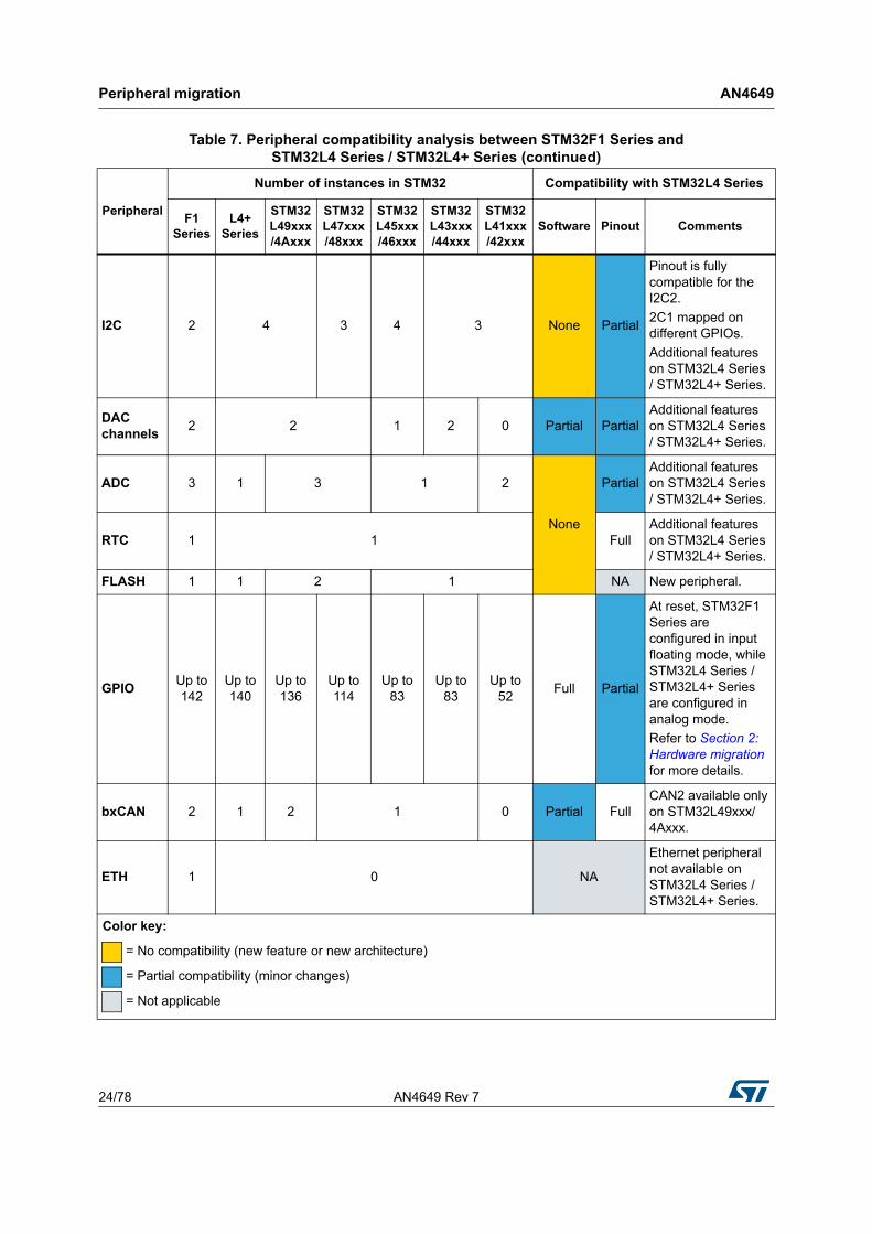
Table 7 gives a general overview of this classification.
The software compatibility mentioned in Table 7 refers only to the register description for low-level drivers.
The STMCube™ hardware abstraction layer (HAL) is compatible between STM32F1 Series and STM32L4 Series / STM32L4+ Series.
Table 7. Peripheral compatibility analysis between STM32F1 Series andSTM32L4 Series / STM32L4+ Series
Peripheral
Number of instances in STM32 Compatibility with STM32L4 Series
F1 Series
L4+ Series
STM32L49xxx/4Axxx
STM32L47xxx/48xxx
STM32L45xxx/46xxx
STM32L43xxx/44xxx
STM32L41xxx/42xxx
Software Pinout Comments
SPI 3 3 2
PartialFull
(SPI)
I2S is no longer supported by SPI but replaced by a dedicated serial audio interface (SAI) in STM32L4 Series / STM32L4+ Series.
The SPI1/SPI2/SPI3 are mapped on the same GPIO.
I2S (full duplex)
3 0

Peripheral migration AN4649
22/78 AN4649 Rev 7
WWDG 1 1 Full
NA
-
IWDG 1 1 Full
Additional read-only window register (IWDG_WINR) in STM32L4 Series / STM32L4+ Series.
DBGMCU 1 1 Full -
CRC 1 1 Partial Additional features in STM32L4 Series / STM32L4+ Series
EXTI 1 1 Partial -
USB OTG FS
1 1 0
Partial Full
Additional features in STM32L4 Series / STM32L4+ Series.
VDDUSB merged with the VDD on STM32F1 Series.
Peripheral only available on STM32F105xx, STM32F107xx, STM32L4Rxxx/ 4Sxxx, STM32L49xxx/ 4Axxx and STM32L47xxx/ 48xxx
USB FS 1 0 1
Additional features in STM32L4 Series / STM32L4+ Series.
VDDUSB merged with VDD on STM32F1 Series.
Peripheral only available on STM32F102xx, STM32F103xx, STM32L45xxx/ 46xxx, STM32L43xxx/ 44xxx and STM32L41xxx/ 42xxx
Table 7. Peripheral compatibility analysis between STM32F1 Series andSTM32L4 Series / STM32L4+ Series (continued)
Peripheral
Number of instances in STM32 Compatibility with STM32L4 Series
F1 Series
L4+ Series
STM32L49xxx/4Axxx
STM32L47xxx/48xxx
STM32L45xxx/46xxx
STM32L43xxx/44xxx
STM32L41xxx/42xxx
Software Pinout Comments

AN4649 Rev 7 23/78
AN4649 Peripheral migration
77
DMA 2 2 None NA
Similar features but the DMA mapping requests are different (see Section 4.3: Direct memory access controller (DMA)).
TIM
Basic
General P.
Advanced
Low-power
IRTIM
2
10
2
0
0
2
7
2
2
1
2
7
2
7
1
2
7
2
2
1
2
4
1
2
1
2
3
1
2
1
1
3
1
2
1
Full Partial
Some pins not mapped on the same GPIO.
Timer instance names may differ.
Internal connections may differ.
SDIO/
SDMMC1 1 0 Partial Full
CE-ATA devices not supported on the STM32L4 Series / STM32L4+ Series.
On STM32F1 Series and STM32L4Rxxx/ 4Sxxx the SDIO is an AHB peripheral, while on STM32L4 Series / STM32L4+ Series, it is an APB peripheral.
FSMC/
FMC1 1 0 Partial Partial
PC card interface not supported on STM32L4 Series / STM32L4+ Series.
One bank of NAND Flash supported on STM32L4 Series / STM32L4+ Series,; two on STM32F1 Series.
PWR 1 1 PartialNA -
RCC 1 1 Partial
USART
UART
LPUART
3
2
0
3
2
1
3
1
1
3
0
1
Partial Full
Additional features on STM32L4 Series / STM32L4+ Series.
Additional LPUART on STM32L4 Series / STM32L4+ Series.
Table 7. Peripheral compatibility analysis between STM32F1 Series andSTM32L4 Series / STM32L4+ Series (continued)
Peripheral
Number of instances in STM32 Compatibility with STM32L4 Series
F1 Series
L4+ Series
STM32L49xxx/4Axxx
STM32L47xxx/48xxx
STM32L45xxx/46xxx
STM32L43xxx/44xxx
STM32L41xxx/42xxx
Software Pinout Comments
Peripheral migration AN4649
24/78 AN4649 Rev 7
I2C 2 4 3 4 3 None Partial
Pinout is fully compatible for the I2C2.
2C1 mapped on different GPIOs.
Additional features on STM32L4 Series / STM32L4+ Series.
DAC channels
2 2 1 2 0 Partial PartialAdditional features on STM32L4 Series / STM32L4+ Series.
ADC 3 1 3 1 2
None
PartialAdditional features on STM32L4 Series / STM32L4+ Series.
RTC 1 1 Full Additional features on STM32L4 Series / STM32L4+ Series.
FLASH 1 1 2 1 NA New peripheral.
GPIOUp to 142
Up to 140
Up to 136
Up to 114
Up to 83
Up to 83
Up to 52
Full Partial
At reset, STM32F1 Series are configured in input floating mode, while STM32L4 Series / STM32L4+ Series are configured in analog mode.
Refer to Section 2: Hardware migration for more details.
bxCAN 2 1 2 1 0 Partial Full CAN2 available only on STM32L49xxx/ 4Axxx.
ETH 1 0 NA
Ethernet peripheral not available on STM32L4 Series / STM32L4+ Series.
Color key:
= No compatibility (new feature or new architecture)
= Partial compatibility (minor changes)
= Not applicable
Table 7. Peripheral compatibility analysis between STM32F1 Series andSTM32L4 Series / STM32L4+ Series (continued)
Peripheral
Number of instances in STM32 Compatibility with STM32L4 Series
F1 Series
L4+ Series
STM32L49xxx/4Axxx
STM32L47xxx/48xxx
STM32L45xxx/46xxx
STM32L43xxx/44xxx
STM32L41xxx/42xxx
Software Pinout Comments

AN4649 Rev 7 25/78
AN4649 Peripheral migration
77
4.2 Memory mapping
The peripheral address mapping has been changed in the STM32L4 Series / STM32L4+ Series versus the STM32F1 Series.
Table 8 provides the peripheral address mapping differences between the STM32F1 Series and the STM32L4 Series / STM32L4+ Series.
Table 8. Peripheral address mapping differences between STM32F1 Series andSTM32L4 Series / STM32L4+ Series
PeripheralSTM32F1 Series
STM32L4 Series / STM32L4+ Series
Bus Base address Bus Base address(1)
FSMC/FMC
AHB
0xA000 0000 AHB3 0xA000 0000
USB OTG FS 0x5000 0000 AHB2 0x5000 0000
ETHERNET MAC 0x4002 8000 NA
CRC 0x4002 3000
AHB1
0x4002 3000
Flash interface reg 0x4002 2000 0x4002 2000
RCC 0x4002 1000 0x4002 1000
DMA2 0x4002 0400 0x4002 0400
DMA1 0x4002 0000 0x4002 0000
SDIO/SDMMC 0x4001 8000 APB20x4001 2800
0x5006 2400 (AHB2) on STM32L4+ Series
TIM11
APB2
0x4001 5400
NATIM10 0x4001 5000
TIM9 0x4001 4C00
ADC3 0x4001 3C00 AHB2 0x5004 0200
USART1 0x4001 3800
APB2
0x4001 3800
TIM8 0x4001 3400 0x4001 3400
SPI1 0x4001 3000 0x4001 3000
TIM1 0x4001 2C00 0x4001 2C00
ADC2
APB2
0x4001 2800
AHB2
0x5004 0100
ADC1 0x4001 2400 0x5004 0000
GPIOG 0x4001 2000 0x4800 1800
GPIOF 0x4001 1C00 0x4800 1400
GPIOE 0x4001 1800 0x4800 1000
GPIOD 0x4001 1400 0x4800 0C00

Peripheral migration AN4649
26/78 AN4649 Rev 7
GPIOC
APB2
0x4001 1000
AHB2
0x4800 0800
GPIOB 0x4001 0C00 0x4800 0400
GPIOA 0x4001 0800 0x4800 0000
EXTI 0x4001 0400 APB2 0x4001 0400
AFIO 0x4001 0000 NA
DAC
APB1
0x4000 7400APB1
0x4000 7400
PWR 0x4000 7000 0x4000 7000
Backup registers (BKP) 0x4000 6C00 NA
bxCAN2 0x4000 6800
APB1
0x4000 6800
bxCAN1 0x4000 6400 0x4000 6400
Shared USB/CAN SRAM 512 bytes
0x4000 6000 0x4000 6C00
USB device FS registers 0x4000 5C00 0x4000 6800
I2C2 0x4000 5800 0x4000 5800
I2C1 0x4000 5400 0x4000 5400
UART5 0x4000 5000 0x4000 5000
UART4 0x4000 4C00 0x4000 4C00
USART3 0x4000 4800 0x4000 4800
USART2 0x4000 4400 0x4000 4400
SPI3/I2S 0x4000 3C00 0x4000 3C00
SPI2/I2S 0x4000 3800 0x4000 3800
IWDG 0x4000 3000 0x4000 3000
WWDG 0x4000 2C00 0x4000 2C00
RTC
(inc. BKP registers on STM32L4 Series / STM32L4+ Series)
APB1
0x4000 2800 APB1 0x4000 2800
TIM14 0x4000 2000
NATIM13 0x4000 1C00
TIM12 0x4000 1800
TIM7 0x4000 1400
APB1
0x4000 1400
TIM6 0x4000 1000 0x4000 1000
TIM5 0x4000 0C00 0x4000 0C00
Table 8. Peripheral address mapping differences between STM32F1 Series andSTM32L4 Series / STM32L4+ Series (continued)
PeripheralSTM32F1 Series
STM32L4 Series / STM32L4+ Series
Bus Base address Bus Base address(1)

AN4649 Rev 7 27/78
AN4649 Peripheral migration
77
TIM4
APB1
0x4000 0800
APB1
0x4000 0800
TIM3 0x4000 0400 0x4000 0400
TIM2 0x4000 0000 0x4000 0000
DMA2D
NA
AHB10x4002 B000
TSC 0x4002 4000
RNG
AHB2
0x5006 0800
HASH 0x5006 0400
AES 0x5006 0000
DCMI 0x5005 0000
GPIOI 0x4800 2000
GPIOH 0x4002 1C00
QUADSPIAHB3
AHB4(2) 0xA000 1000
SYSCFG
APB2
0x4001 0000
DFSDM 0x4001 6000
SAI1 0x4001 5400
SAI2 0x4001 5800
TIM17 0x4001 4800
TIM16 0x4001 4400
TIM15 0x4001 4000
FIREWALL 0x4001 1C00
VREF 0x4001 0030
COMP 0x4001 0200
OPAMP
APB1
0x4000 7800
I2C3 0x4000 5C00
LCD 0x4000 2400
LPTIM2 0x4000 9400
SWPMI1 0x4000 8800
I2C4 0x4000 8400
LPUART1 0x4000 8000
LPTIM1 0x4000 7C00
CRS 0x40006000
Table 8. Peripheral address mapping differences between STM32F1 Series andSTM32L4 Series / STM32L4+ Series (continued)
PeripheralSTM32F1 Series
STM32L4 Series / STM32L4+ Series
Bus Base address Bus Base address(1)

Peripheral migration AN4649
28/78 AN4649 Rev 7
The system memory mapping has been updated between STM32F1 Series and STM32L4 Series / STM32L4+ Series. Refer to reference manuals or datasheets for more details.
STM32L4 Series / STM32L4+ Series feature an additional SRAM (SRAM2) of 64 Kbytes on STM32L4+ Series, STM32L49xxx/4Axxx devices, 32 Kbytes on STM32L47xxx/48xxx and STM32L45xxx/46xxx devices, 16 Kbytes on STM32L43xxx/44xxx and 8 Kbytes on STM32L41xxx/42xxx devices and an additional SRAM (SRAM3) of 384 Kbytes on STM32L4+ Series.
The SRAM2 includes the additional features listed below:
• Maximum performance through ICode bus access without physical remap
• Parity check option (32-bit + 4-bit parity check)
• Write protection with 1 Kbyte granularity
• Read protection (RDP)
• Erase by system reset (option byte) or by software
• Content is preserved in Low-power run, Low-power sleep, Stop 0, Stop 1, Stop 2 mode
• Content can be preserved (RRS bit set in PWR_CR3 register) in Standby mode (not the case for SRAM1).
OCTOSPI2
NA
AHB30xA000 1400
OCTOSPI1 0xA000 1000
OCTOSPIM AHB2 0x5006 1C00
GFXMMUAHB1
0x4002 C000
DMAMUX1 0x4002 0800
DSIHOSTAPB2
0x4001 6C00
LCD-TFT 0x4001 6800
Color key:
= Base address or bus change
= Not applicable
1. On STM32L4 Series / STM32L4+ Series devices on which the peripheral is not implemented, the memory address is reserved.
2. AHB3 for STM32L47xxx/48xxx, STM32L45xxx/46xxx and STM32L43xxx/44xxx devices, AHB4 for STM32L49xxx/4Axxx devices.
Table 8. Peripheral address mapping differences between STM32F1 Series andSTM32L4 Series / STM32L4+ Series (continued)
PeripheralSTM32F1 Series
STM32L4 Series / STM32L4+ Series
Bus Base address Bus Base address(1)

AN4649 Rev 7 29/78
AN4649 Peripheral migration
77
4.3 Direct memory access controller (DMA)
STM32F1 Series and STM32L4 Series / STM32L4+ Series have the same DMA IP.
The current consumption of the DMA on STM32L4 Series / STM32L4+ Series has been slightly improved compared to the consumption on STM32F1 Series, and it includes option registers.
Table 9 presents the differences between the DMA requests of the peripherals in STM32F1 Series and STM32L4 Series / STM32L4+ Series.
Table 9. DMA request differences between STM32F1 Series andSTM32L4 Series / STM32L4+ Series
Peripheral DMA request STM32F1 SeriesSTM32L4 Series /
STM32L4+ Series(1)
ADC
ADC1 DMA1_Channel1DMA1_Channel1
DMA2_Channel3
ADC2 NADMA1_Channel2
DMA2_Channel4
ADC3 DMA2_Channel5DMA1_Channel3
DMA2_Channel5
DAC
DAC1_CH1 DMA2_Channel3DMA1_Channel3
DMA2_Channel4
DAC1_CH2 DMA2_Channel4DMA1_Channel4
DMA2_Channel5
DFSDM
DFSDM0
NA
DMA1_Channel4
DFSDM1 DMA1_Channel5
DFSDM2 DMA1_Channel6
DFSDM3 DMA1_Channel7
SPI1
SPI1_Rx DMA1_Channel2DMA1_Channel2
DMA2_Channel3
SPI1_Tx DMA1_Channel3DMA1_Channel3
DMA2_Channel4
SPI2SPI2_Rx
SPI2_Tx
DMA1_Channel4
DMA1_Channel5
DMA1_Channel4
DMA1_Channel5
SPI3SPI3_Rx
SPI3_Tx
DMA2_Channel1
DMA2_Channel2
DMA2_Channel1
DMA2_Channel2
QUADSPI QUADSPI
NA
DMA2_Channel7
DMA1_Channel5
LPUARTLPUART_RX NA
LPUART_TX
DMA2_Channel7
DMA2_Channel6

Peripheral migration AN4649
30/78 AN4649 Rev 7
USART1
USART1_Rx DMA1_Channel5DMA1_Channel5
DMA2_Channel7
USART1_Tx DMA1_Channel4DMA1_Channel4
DMA2_Channel6
USART2USART2_Rx
USART2_Tx
DMA1_Channel6
DMA1_Channel7
DMA1_Channel6
DMA1_Channel7
USART3USART3_Rx
USART3_Tx
DMA1_Channel3
DMA1_Channel2
DMA1_Channel3
DMA1_Channel2
UART4UART4_Rx
UART4_Tx
DMA2_Channel3
DMA2_Channel5
DMA2_Channel5
DMA2_Channel3
UART5UART5_Rx
UART5_TxNA
DMA2_Channel2
DMA2_Channel1
I2C1
I2C1_Rx DMA1_Channel7DMA1_Channel7
DMA2_Channel6
I2C1_Tx DMA1_Channel6DMA1_Channel6
DMA2_Channel7
I2C2I2C2_Rx
I2C2_Tx
DMA1_Channel5
DMA1_Channel4
DMA1_Channel5
DMA1_Channel4
I2C3I2C3_Rx
I2C3_TxNA
DMA1_Channel3
DMA1_Channel2
I2C4I2C4_Rx
I2C4_Tx
DMA2_Channel1
DMA2_Channel2
SDIO
SDMMC
SDIO DMA2_Channel4 NA
SDMMC NADMA2_Channel4
DMA2_Channel5
TIM1
TIM1_UP
TIM1_TRIG
TIM1_COM
TIM1_CH1
TIM1_CH3
TIM1_CH4
DMA1_Channel5
DMA1_Channel4
DMA1_Channel4
DMA1_Channel2
DMA1_Channel6
DMA1_Channel4
DMA1_Channel6
DMA1_Channel4
DMA1_Channel4
DMA1_Channel2
DMA1_Channel7
DMA1_Channel4
TIM2
TIM2_UP
TIM2_CH1
TIM2_CH2
TIM2_CH3
TIM2_CH4
DMA1_Channel2
DMA1_Channel5
DMA1_Channel7
DMA1_Channel1
DMA1_Channel7
DMA1_Channel2
DMA1_Channel5
DMA1_Channel7
DMA1_Channel1
DMA1_Channel7
Table 9. DMA request differences between STM32F1 Series andSTM32L4 Series / STM32L4+ Series (continued)
Peripheral DMA request STM32F1 SeriesSTM32L4 Series /
STM32L4+ Series(1)

AN4649 Rev 7 31/78
AN4649 Peripheral migration
77
TIM3
TIM3_UP
TIM3_TRIG
TIM3_CH1
TIM3_CH3
TIM3_CH4
DMA1_Channel3
DMA1_Channel6
DMA1_Channel6
DMA1_Channel2
DMA1_Channel3
DMA1_Channel3
DMA1_Channel6
DMA1_Channel6
DMA1_Channel2
DMA1_Channel3
TIM4
TIM4_UP
TIM4_CH1
TIM4_CH2
TIM4_CH3
DMA1_Channel7
DMA1_Channel1
DMA1_Channel4
DMA1_Channel5
DMA1_Channel7
DMA1_Channel1
DMA1_Channel4
DMA1_Channel5
TIM5
TIM5_UP
TIM5_CH1
TIM5_CH2
TIM5_CH3
TIM5_CH4
TIM5_TRIG
TIM5_COM
DMA2_Channel2
DMA2_Channel5
DMA2_Channel4
DMA2_Channel2
DMA2_Channel1
DMA2_Channel1
NA
DMA2_Channel2
DMA2_Channel5
DMA2_Channel4
DMA2_Channel2
DMA2_Channel1
DMA2_Channel1
DMA2_Channel1
TIM6 TIM6_UP DMA2_Channel3DMA1_Channel3
DMA2_Channel4
TIM7 TIM7_UP DMA2_Channel4DMA1_Channel4
DMA2_Channel5
TIM8
TIM8_UP
TIM8_CH1
TIM8_CH2
TIM8_CH3
TIM8_CH4
TIM8_TRIG TIM8_COM
DMA2_Channel1
DMA2_Channel3
DMA2_Channel5
DMA2_Channel1
DMA2_Channel2
DMA2_Channel2
DMA2_Channel2
DMA2_Channel1
DMA2_Channel6
DMA2_Channel7
DMA2_Channel1
DMA2_Channel2
DMA2_Channel2
DMA2_Channel2
TIM15
TIM15_CH1
TIM15_UP
TIM15_TRIG
TIM15_COM
NA
DMA1_Channel5
DMA1_Channel5
DMA1_Channel5
DMA1_Channel5
TIM16
TIM16_CH1
TIM16_UP
TIM16_CH1
TIM16_UP
DMA1_Channel3
DMA1_Channel3
DMA1_Channel6
DMA1_Channel6
TIM17
TIM17_CH1
TIM17_UP
TIM17_CH1
TIM17_UP
DMA1_Channel1
DMA1_Channel1
DMA1_Channel7
DMA1_Channel7
Table 9. DMA request differences between STM32F1 Series andSTM32L4 Series / STM32L4+ Series (continued)
Peripheral DMA request STM32F1 SeriesSTM32L4 Series /
STM32L4+ Series(1)

Peripheral migration AN4649
32/78 AN4649 Rev 7
4.4 Interrupts
Table 10 presents the interrupt vectors in STM32L4 Series / STM32L4+ Series compared to STM32F1 Series.
The changes in the interrupt vectors impact only a few peripherals.
SAI
SAI1_A
NA
DMA2_Channel1
DMA2_Channel6
SAI1_B DMA2_Channel2
DMA2_Channel7
SAI2_A DMA1_Channel6
DMA2_Channel3
SAI2_B DMA1_Channel7
DMA2_Channel4
SWPMISWPMI_RX DMA2_Channel1
SWPMI_TX DMA2_Channel2
AES
AES_OUTDMA2_Channel3
DMA2_Channel2
AES_INDMA2_Channel5
DMA2_Channel1
DCMI DCMIDMA2_Channel7
DMA2_Channel5
HASH HASH_IN DMA2_Channel7
Color key:
= Feature not available (NA)
= Differences
1. On the STM32L4 Series / STM32L4+ Series devices on which the peripheral is not implemented, the DMA request is reserved.
Table 9. DMA request differences between STM32F1 Series andSTM32L4 Series / STM32L4+ Series (continued)
Peripheral DMA request STM32F1 SeriesSTM32L4 Series /
STM32L4+ Series(1)
Table 10. Interrupt vector differences between STM32F1 Seriesand STM32L4 Series / STM32L4+ Series
Position
STM32F1 Series
STM32L4 Series / STM32L4+ Series(1)STM32F105 and
STM32F107 linesConnectivity
STM32F101and STM32F103 lines
XL density(2)
STM32F100 and STM32F102 lines
0 WWDG WWDG
1 PVD PVD / PVM

AN4649 Rev 7 33/78
AN4649 Peripheral migration
77
2 TAMPER TAMPER / CSS
3 RTC RTC_WKUP
4 FLASH FLASH
5 RCC RCC
6 EXTI0 EXTI0
7 EXTI1 EXTI1
8 EXTI2 EXTI2
9 EXTI3 EXTI3
10 EXTI4 EXTI4
11 DMA1_Channel1 DMA1_Channel1
12 DMA1_Channel2 DMA1_Channel2
13 DMA1_Channel3 DMA1_Channel3
14 DMA1_Channel4 DMA1_Channel4
15 DMA1_Channel5 DMA1_Channel5
16 DMA1_Channel6 DMA1_Channel6
17 DMA1_Channel7 DMA1_Channel7
18 ADC1_2 ADC1_2
19 CAN1_TX USB_HP / CAN_TX CAN1_TX
20 CAN1_RX0 USB_LP /CAN_RX0 CAN1_RX0
21 CAN1_RX1 CAN_RX1 CAN1_RX1
22 CAN1_SCE CAN_SCE CAN1_SCE
23 EXTI9_5 EXTI9_5
24 TIM1_BRK TIM1_BRK / TIM9 TIM1_BRK TIM1_BRK / TIM15
25 TIM1_UP TIM1_UP / TIM10 TIM1_UP TIM1_UP / TIM16
26 TIM1_TRG_COMTIM1_TRG_COM /
TIM11TIM1_TRG_COM
TIM1_TRG_COM /TIM17
27 TIM1_CC TIM1_CC
28 TIM2 TIM2
29 TIM3 TIM3
30 TIM4 TIM4
31 I2C1_EV I2C1_EV
32 I2C1_ER I2C1_ER
Table 10. Interrupt vector differences between STM32F1 Seriesand STM32L4 Series / STM32L4+ Series (continued)
Position
STM32F1 Series
STM32L4 Series / STM32L4+ Series(1)STM32F105 and
STM32F107 linesConnectivity
STM32F101and STM32F103 lines
XL density(2)
STM32F100 and STM32F102 lines

Peripheral migration AN4649
34/78 AN4649 Rev 7
33 I2C2_EV I2C2_EV
34 I2C2_ER I2C2_ER
35 SPI1 SPI1
36 SPI2 SPI2
37 USART1 USART1
38 USART2 USART2
39 USART3 USART3
40 EXTI15_10 EXTI15_10
41 RTC_Alarm RTC_Alarm
42 USB_FS_WKUP USBWakeup DFSDM3
43
NA
TIM8_BRK / TIM12 TIM8_BRK TIM8_BRK
44 TIM8_UP / TIM13 TIM8_UP TIM8_UP
45TIM8_TRG_COM /
TIM14TIM8_TRG_COM TIM8_TRG_COM
46 TIM8_CC TIM8_CC
47 ADC3 ADC3
48 FSMC FMC
49 SDIO SDMMC
50 TIM5 TIM5
51 SPI3 SPI3
52 UART4 UART4
53 UART5 UART5
54 TIM6 TIM6_DACUNDER
55 TIM7 TIM7
56 DMA2_Channel1 DMA2_Channel1
57 DMA2_Channel2 DMA2_Channel2
58 DMA2_Channel3 DMA2_Channel3
59 DMA2_Channel4 DMA2_Channel4_5 DMA2_Channel4
Table 10. Interrupt vector differences between STM32F1 Seriesand STM32L4 Series / STM32L4+ Series (continued)
Position
STM32F1 Series
STM32L4 Series / STM32L4+ Series(1)STM32F105 and
STM32F107 linesConnectivity
STM32F101and STM32F103 lines
XL density(2)
STM32F100 and STM32F102 lines

AN4649 Rev 7 35/78
AN4649 Peripheral migration
77
60 DMA2_Channel5
NA
DMA2_Channel5
61 ETH DFSDM0
62 ETH_WKUP DFSDM1
63 CAN2_TX DFSDM2
64 CAN2_RX0 COMP
65 CAN2_RX1 LPTIM1
66 CAN2_SCE LPTIM2
67 OTG_FS
– OTG_FS on STM32L4Rxxx/ 4Sxxx, STM32L49xxx/4Axxx and STM32L47xxx/48xxx
– USB_FS on STM32L45xxx/46xxx,STM32L43xxx/44xxx and STM32L41xxx/42xxx
68
NA
DMA2_CH6
69 DMA2_CH7
70 LPUART1
71
– QUADSPI
– OCTOSPI 1 (for STM32L4Rxxx/ 4Sxxx)
72 I2C3_EV
73 I2C3_ER
74 SAI1
75 SAI2
76
– SWPMI1
– OCTOSPI2 (for STM32L4Rxxx /4Sxxx)
77 TSC
78
– LCD
– DSIHOST (for STM32L4R9xx/ 4S9xx)
Table 10. Interrupt vector differences between STM32F1 Seriesand STM32L4 Series / STM32L4+ Series (continued)
Position
STM32F1 Series
STM32L4 Series / STM32L4+ Series(1)STM32F105 and
STM32F107 linesConnectivity
STM32F101and STM32F103 lines
XL density(2)
STM32F100 and STM32F102 lines

Peripheral migration AN4649
36/78 AN4649 Rev 7
79
NA
AES
80 HASH_RNG
81 FPU
82 HASH and CRS
83 I2C4_EV
84 I2C4_ER
85 DCMI
86 CAN2_TX
87 CAN2_RX0
88 CAN2_RX1
89 CAN2_SCE
90 DMA2D
91 LCD-TFT
92 LCD-TFT_ER
93 GFXMMU
94 DMAMUX1_OVR
Color key:
= Same feature, but specification change or enhancement
= Feature not available (NA)
= Differences
1. On the STM32L4 Series / STM32L4+ Series devices on which the peripheral is not implemented, the interrupt is not applicable.
2. Flash memory density ranges between 768 Kbytes and 1 Mbyte.
Table 10. Interrupt vector differences between STM32F1 Seriesand STM32L4 Series / STM32L4+ Series (continued)
Position
STM32F1 Series
STM32L4 Series / STM32L4+ Series(1)STM32F105 and
STM32F107 linesConnectivity
STM32F101and STM32F103 lines
XL density(2)
STM32F100 and STM32F102 lines

AN4649 Rev 7 37/78
AN4649 Peripheral migration
77
4.5 Reset and clock control (RCC)
The main differences related to the RCC between STM32L4 Series / STM32L4+ Series and STM32F1 Series, are presented inTable 11 below.
Table 11. RCC differences between STM32F1 Seriesand STM32L4 Series / STM32L4+ Series
RCC STM32F1 Series STM32L4 Series / STM32L4+ Series
MSI NA
– The MSI is a low-power oscillator with a programmable frequency of up to 48 MHz. It can replace the PLL as system clock (faster wakeup, lower consumption). It can be used as USB device clock (no need for external high-speed crystal oscillator).
– Multi speed RC factory and user trimmed (100 kHz, 200 kHz, 400 kHz, 800 kHz, 1 MHz, 2 MHz, 4 MHz (default value), 8 MHz, 16 MHz, 24 MHz, 32 MHz and 48 MHz).
– Auto calibration from LSE.
HSI16 8 MHz RC factory and user trimmed. 16 MHz RC factory and user trimmed.
LSI 40 kHz RC.– 32 kHz RC.
– Lower consumption, higher accuracy (refer to product datasheet).
HSE
– Connectivity lines:(1) 3 - 25 MHz.
– Other lines: 4 - 16 MHz (up to 25 MHz in bypass mode).
4 - 48 MHz.
HSI48 NA
– 48 MHz RC Only for STM32L4+ Series, STM32L49xxx/4Axxx, STM32L45xxx/46xxx, STM32L43xxx/44xxx and STM32L41xxx/42xxx.
– Can drive USB Full Speed, SDMMC and RNG.
LSE– 32.768 kHz (up to 1 MHz in bypass
mode).
– Available in backup domain (VBAT).
– 32.768 kHz (up to 1 MHz in bypass mode).
– Configurable drive/consumption.
– Available in backup domain (VBAT).

Peripheral migration AN4649
38/78 AN4649 Rev 7
PLL
– Connectivity lines:(1) 3 PLLs Main PLL sources: HSI/2, HSE, PLL2 (through divider) PLL2, PLL3 clocked by HSE through divider
– Other lines: 1 PLL The PLL sources are HSI, HSE.
– Main PLL for system
– 2 PLLs for SAI1/2, ADC, RNG, SDMMC and OTG FS clock. (for STM32L4+ Series, STM32L49xxx/4Axxx and STM32L47xxx/48xxx)
– 1 PLL for SAI1, ADC, RNG, SDMMC, USB FS clock (for STM32L45xxx/46xxx and STM32L43xxx/44xxx)
Each PLL can provide up to 3 independent outputs.
The PLL sources are MSI, HSI16, HSE.
System clock source
HSI, HSE or PLL. MSI, HSI16, HSE or PLL.
System clock frequency
– Up to 72 MHz.
– 8 MHz after reset using HSI.
– Up to 80 MHz or 120 for STM32L4+ Series.
– 4 MHz after reset using MSI.
AHB frequency
Up to 72 MHz.Up to 80 MHz or 120 for STM32L4+ Series.
APB1 frequency
Up to 36 MHz.Up to 80 MHz or 120 MHz for STM32L4+ Series.
APB2 frequency
Up to 72 MHz.Up to 80 MHz or 120 MHz for STM32L4+ Series.
RTC clock source
LSI, LSE or HSE/128. LSI, LSE or HSE/32.
MCO clock source
– MCO1 pin (PA8): (max 50 MHz)
– Connectivity lines:(1) HSI, HSE, SYSCLK, PLLCLK/2, PLL2, PLL3/2, XT1 ext 3-25 MHz, PLL3.
– Other lines: HSI, HSE, SYSCLK, PLLCLK/2.
– MCO pin (PA8): SYSCLK, HSI16, HSE, PLLCLK, MSI, LSE, LSI or HSI48 (for STM32L4+ Series, STM32L49xxx/4Axxx, STM32L45xxx/46xxx, STM32L44xxx/43xxx and STM32L41xxx/42xxx).
– With configurable prescaler, 1, 2, 4, 8 or 16 for each output.
CSS– CSS (clock security system).
– CSS on HSE.
– CSS (clock security system).
– CSS on LSE.
Table 11. RCC differences between STM32F1 Seriesand STM32L4 Series / STM32L4+ Series (continued)
RCC STM32F1 Series STM32L4 Series / STM32L4+ Series

AN4649 Rev 7 39/78
AN4649 Peripheral migration
77
In addition to the differences described in Table 11, the following additional adaptation steps may be needed for the migration:
• Maximum clock frequency versus Flash wait state
• Peripheral access configuration
• Peripheral clock configuration
Internal oscillator measurement / calibration
– LSE connected to TIM5 CH4 IC: can measure HSI with respect to LSE clock high precision.
– LSI connected to TIM5 CH4 IC: can measure LSI with respect to HSI or HSE clock precision.
– HSE connected to TIM11 CH1 IC: can measure HSE with respect to LSE/HSI clock.
– LSE connected to TIM15 or TIM16 CH1 IC: can measure HSI16 or MSI with respect to LSE clock high precision.
– LSI connected to TIM16 CH1 IC: can measure LSI with respect to HSI16 or HSE clock precision.
– HSE/32 connected to TIM17 CH1 IC: can measure HSE with respect to LSE/HSI16 clock.
– MSI connected to TIM17 CH1 IC: can measure MSI with respect to HSI16/HSE clock .
– On STM32L45xxx/46xxx and STM32L43xxx/44xxx devices, HSE/32 and MSI connected to TIM16 CH1 IC.
Interrupt
– CSS (linked to NMI IRQ).
– LSIRDY, LSERDY, HSIRDY, HSERDY, PLLRDY (linked to RCC global IRQ).
– CSS (linked to NMI IRQ).
– LSECSS, LSIRDY, LSERDY, HSIRDY, MSIRDY, HSERDY, PLLRDY, PLLSAI1RDY, PLLSAI2RDY (only on STM32L4+ Series, STM32L49xxx/4Axxx and STM32L47xxx/48xxx) (linked to RCC global IRQ).
Color key:
= New feature or new architecture (difference between STM32F1 and STM32L4)
= Same feature, but specification change or enhancement
= Feature not available (NA)
= Differences.
1. Connectivity = STM32F105xx and STM32F107xx lines.
Table 11. RCC differences between STM32F1 Seriesand STM32L4 Series / STM32L4+ Series (continued)
RCC STM32F1 Series STM32L4 Series / STM32L4+ Series

Peripheral migration AN4649
40/78 AN4649 Rev 7
4.5.1 Performance versus VCORE ranges
In STM32L4 Series / STM32L4+ Series, the maximum CPU clock frequency and the maximum number of Flash memory wait state depend on the selected VCORE voltage range.
On STM32F1 Series, the maximum system-clock frequency and the maximum number of Flash memory wait-state are linked by the conditions below:
• Zero wait state, if 0 < HCLK ≤ 24 MHz
• One wait state, if 24 MHz < HCLK ≤ 48 MHz
• Two wait states, if 48 MHz < HCLK ≤ 72 MHz.
Table 12. Performance versus VCORE ranges for STM32L4 Series and STM32L4+ Series
CPU
performancePower
performanceVCORE range
Typical value (V)
Max frequency (MHz)
5 WS 4 WS 3 WS 2 WS 1 WS 0 WS
STM32L4 Series
High Medium 1 1.2 - 80 64 48 32 16
Medium High 2 1.0 - 26 26 18 12 6
STM32L4+ Series
High Medium
1 boost mode
1.28 120 100 80 60 40 20
1 normal mode
1.2 - - 80 60 40 20
Medium High 2 1.0 - - - 26 16 8

AN4649 Rev 7 41/78
AN4649 Peripheral migration
77
4.5.2 Peripheral access configuration
Since the address mapping of some peripherals has been changed in STM32L4 Series / STM32L4+ Series compared to STM32F1 Series, different registers need to be used to [enable/disable] or [enter/exit] the peripheral [clock] or [from reset mode].
The configuration to access a given peripheral involves:
• Identifying the bus to which the peripheral is connected (refer to Table 8)
• Selecting the right register according to the needed action (refer to Table 13).
The USART1 is connected to the APB2 bus. To enable the USART1 clock, the RCC_APB2ENR register needs to be configured with the STM32Cube HAL driver RCC API:
__HAL_RCC_USART1_CLK_ENABLE();
To disable the USART1 clock during Sleep mode (to reduce power consumption) the RCC_APB2SMENR register must be configured with the STM32Cube HAL driver RCC API:
__HAL_RCC_USART1_CLK_SLEEP_ENABLE();
Table 13. RCC registers used for peripheral access configuration for STM32F1 Seriesand STM32L4 Series / STM32L4+ Series
BusRegister
STM32F1 Series
Register
STM32L4 Series / STM32L4+ Series
Comments
AHB
RCC_AHBRSTR
RCC_AHB1RSTR (AHB1)
RCC_AHB2RSTR (AHB2)
RCC_AHB3RSTR (AHB3)
Used to [enter/exit] the AHB peripheral from reset
RCC_AHBENR
RCC_AHB1ENR (AHB1)
RCC_AHB2ENR (AHB2)
RCC_AHB3ENR (AHB3)
Used to [enable/disable] the AHB peripheral clock
NA
RCC_AHB1SMENR (AHB1)
RCC_AHB2SMENR (AHB2)
RCC_AHB3SMENR (AHB3)
Used to [enable/disable] the AHB peripheral clock in Sleep mode
APB1
RCC_APB1RSTRRCC_APB1RSTR1
RCC_APB1RSTR2Used to [enter/exit] the APB1 peripheral from reset
RCC_APB1ENRRCC_APB1ENR1
RCC_APB1ENR2Used to [enable/disable] the APB1 peripheral clock
NARCC_APB1SMENR1
RCC_APB1SMENR2Used to [enable/disable] the APB1 peripheral clock in Sleep mode
APB2
RCC_APB2RSTRUsed to [enter/exit] the APB2 peripheral from reset
RCC_APB2ENRUsed to [enable/disable] the APB2 peripheral clock
NA RCC_APB2SMENRUsed to [enable/disable] the APB2 peripheral clock in Sleep mode
Color key:
= Feature not available (NA)

Peripheral migration AN4649
42/78 AN4649 Rev 7
4.5.3 Peripheral clock configuration
Some peripherals have a dedicated clock-source independent from the system clock, which is used to generate the clock required for their operation:
• USB:
In STM32F1 Series, the USB 48 MHz clock is derived from the main PLL VCO output.
In STM32L4 Series and STM32L4+ Series, the USB 48 MHz clock is derived from one of the following sources:
– Main PLL VCO (PLLUSB1CLK)
– PLLSAI1 VCO (PLLUSB2CLK)
– MSI clock (when the MSI clock is auto-trimmed with the LSE, it can be used by the USB OTG FS device)
– HSI48 internal oscillator (only on STM32L4+ Series, STM32L4+ Series, STM32L49xxx/4Axxx, STM32L45xxx/46xxx, STM32L43xxx/44xxx and STM32L41xxx/42xxx).
• SDIO/SDMMC:
In STM32F1 Series (except for connectivity devices), the SDIO AHB interface clock (SDIOCLK) is derived from the system clock and is equal to HLCK/2 (HCLK = AHB clock), while the SDIO adapter clock equals HCLK.
In STM32L4 Series and STM32L4+ Series, the SDMMC clock is derived from one of the following sources:
– Main PLL VCO (PLLUSB1CLK)
– PLLSAI1 VCO (PLLUSB2CLK)
– MSI clock
– HSI48 internal oscillator (only on STM32L49xxx/4Axxx, STM32L45xxx/46xxx and STM32L43xxx/44xxx).
• RTC:
In STM32F1 Series, the RTC clock is derived from one of the following sources: LSE clock, LSI clock or HSE divided by 128.
In STM32L4 Series and STM32L4+ Series, the RTC and the LCD glass clocks are derived from one of the three following sources: LSE clock, LSI clock, or HSE clock divided by 32. The PCLK frequency must always be greater than or equal to the RTC clock frequency.
• ADC:
In STM32F1 Series, the ADC clock is the PCLK2 clock divided by a programmable factor (2, 4, 6, 8). In STM32L4 Series and STM32L4+ Series, the input clock of the two ADCs (master and slave) can be selected between different clock sources (two for STM32L43xxx/44xxx, STM32L45xxx/46xxx and three for STM32L47xxx/48xxx):
– Derived (selected by software) from system clock (SYSCLK), PLLSAI1 VCO(a) (PLLADC1CLK) or PLLSAI2 VCO(b) (PLLADC2CLK) (only on STM32L4+ Series, STM32L49xxx/4Axxx and STM32L47xxx/48xxx). In this mode, a programmable divider factor can be selected (1, 2, …, 256 according to bits PREC[3:0]).
a. Not available on STM32L41xxx/42xxx, only STSCLK can be used on those devices.
b. PLLSAI2VCO (PLLADC2CLK) is a clock source only on STM32L49xxx/4Axxx and STM32L47xxx/48xxx.

AN4649 Rev 7 43/78
AN4649 Peripheral migration
77
– Derived from the AHB clock of the ADC bus interface, divided by a programmable factor (1, 2 or 4). In this mode, a programmable divider factor can be selected (1, 2 or 4 according to bits CKMODE[1:0]). Refer to the STM32L4 Series and STM32L4+ Series reference manual for more details.
• DAC:
In STM32L4 Series and STM32L4+ Series in addition to the PCLK1 clock, the LSI clock is used for the sample and hold operation.
• U(S)ARTs:
In STM32F1 Series, the U(S)ART clock is APB1 or APB2 clock, depending on which APB bus is mapped to the U(S)ART.
In STM32L4 Series and STM32L4+ Series, the U(S)ART clock is derived from one of the four following sources: system clock (SYSCLK), HSI16, LSE, APB1 or APB2 clock (depending on which APB bus is mapped to the U(S)ART).
Using a source clock independent from the system clock (example: HSI16) allows to change the system clock on the fly without the need to reconfigure U(S)ART peripheral baud rate prescalers.
• I2Cs:
In STM32L4 Series and STM32L4+ Series, the I2C clock is derived from one of the three following sources: system clock (SYSCLK), HSI16 or APB1 (PCLK1).
Using a source clock independent from the system clock (example HSI16) allows to change the system clock on the fly without need to reconfigure I2C peripheral timing register.
• I2S/SAI:
In STM32F1 Series, the I2S clocks are derived from one of the two following sources:
– SYSCLK (system clock)
– PLL3VCO (= 2x PLL3CLK) (only on connectivity devices).
In STM32L4 Series and STM32L4+ Series, the I2S peripherals are not available and replaced by SAIs.
For STM32L4+ Series, STM32L49xxx/4Axxx and STM32L47xxx/48xxx, the SAI clocks are derived from one of the four following sources:
– An external clock mapped on SAI1_EXTCLK or SAI2_EXTCLK
– PLLSAI1 VCO (PLLSAI1CLK)
– PLLSAI2 VCO (PLLSAI2CLK)
– A main PLL VCO (PLLSAI3CLK)
For STM32L45xxx/46xxx and STM32L43xxx/44xxx devices, the SAI clocks are derived from one of the four following sources:
– An external clock mapped on SAI1_EXTCLK for SAI1
– PLLSAI1 (P) divider output (PLLSAI1CLK)
– A main PLL (P) divider output (PLLSAI2CLK)
– HSI16 clock
• IWDG:
In STM32F1 Series and STM32L4 Series / STM32L4+ Series, the IWDG clock is LSI.
• Ethernet:
Ethernet clocks are not available on STM32L4 Series / STM32L4+ Series compared to STM32F1 Series (no Ethernet peripheral on STM32L4 Series / STM32L4+ Series).

Peripheral migration AN4649
44/78 AN4649 Rev 7
4.6 Power control (PWR )
In STM32L4 Series / STM32L4+ Series, the PWR controller presents some differences versus the one in STM32F1 Series. These differences are summarized in Table 14.
Table 14. PWR differences between STM32F1 Series and STM32L4 Series / STM32L4+ Series
PWR STM32F1 Series STM32L4 Series / STM32L4+ Series
Power supplies
VDD = 2.0 to 3.6 V: external power supply for I/Os, Flash memory and internal regulator. It is provided externally through VDD pins.
VDD = 1.71 to 3.6 V: external power supply for I/Os and internal regulator. It is provided externally through VDD pins.
– VCORE = 1.8 V
– VCORE is the power supply for digital peripherals, SRAM and Flash memory. It is generated by an internal voltage regulator.
– In Stop mode the regulator supplies low-power preserving contents of registers and SRAM.
– VCORE = 1.0 to 1.28 V
– VCORE is the power supply for digital peripherals, SRAM and Flash memory. It is generated by an internal voltage regulator. Two VCORE ranges can be selected by software depending on target frequency.
VBAT = 1.8 to 3.6 V: power supply for RTC, external clock 32 kHz oscillator and backup registers (through power switch) when VDD is not present.
VBAT = 1.55 to 3.6 V: power supply for RTC, external clock 32 kHz oscillator and backup registers (through power switch) when VDD is not present.
VDD and VDDA must be at the same voltage value.
Independent power supplies (VDDA, VDDUSB, VDDIO2) allow to improve power consumption by running MCU at lower supply voltage than analog and USB.
– VSSA, VDDA: 2.0 V to 3.6 V
– VDDA is the external analog power supply for A/D and D/A converters. VDDA and VSSA must be connected to VDD and VSS respectively.
– VSSA, VDDA = 1.62 V (ADCs/COMPs) to 3.6 V 1.8 V (DAC/OPAMPs) to 3.6 V 2.4 V (VREFBUF) to 3.6 V
– VDDA is the external analog power supply for A/D and D/A converters, voltage reference buffer, operational amplifiers and comparators. The VDDA voltage level is independent from the VDD voltage.
NA
– VLCD = 2.5 to 3.6 V
– The LCD controller can be powered either externally through the VLCD pin or internally from an internal voltage generated by the embedded step-up converter.
– NA
– USB powered by VDD.
VDD must be > 3.0 V (or degraded electrical characteristic between 2.7 V to 3 V)
– VDDUSB = 3.0 to 3.6 V
– VDDUSB is the external independent power supply for USB transceivers. The VDDUSB voltage level is independent from the VDD voltage.

AN4649 Rev 7 45/78
AN4649 Peripheral migration
77
Power supplies (continuation)
– N/A
– No VDDIO2 supply on STM32F1 Series.
– VDDIO2 = 1.08 V to 3.6 V
– V DDIO2 is the external power supply for 14 I/Os (Port G[15:2]). The V DDIO2 voltage level is independent from the VDD voltage. Not applicable for STM32L45xxx/46xxx, STM32L43xxx/44xxx and STM32L41xxx/42xxx devices.
NA
– Available only on SM32L4R9xx/4S9xx.
– VDDDSI is independent DSI power supply dedicated for the DSI regulator and the MIPI D-PHY. This supply must be connected to the global VDD.
NA
– Available only on SM32L4R9xx/4S9xx.
– VCAPDSI is the output of the DSI regulator (1.2 V) which must be connected externally to VDD12DSI.
NA
– Available only on SM32L4R9xx/4S9xx.
– VDD12DSI is used to supply the MIPI D-PHY, and to supply the clock and data lanes pins. An external capacitor of 2.2µF must be connected on the VDD12DSI pin.
Battery backup domain
– RTC with backup registers
– LSE
– PC13 to PC15 I/Os
– RTC with backup registers
– LSE
– PC13 to PC15 I/Os
– Data retention on SRAM2 during Standby
Power supply supervisor
– Integrated POR / PDR circuitry
– Programmable voltage detector (PVD)
– Integrated POR / PDR circuitry
– Programmable voltage detector (PVD)
NA
– Brownout reset (BOR)
– BOR is always enabled, except in Shutdown mode
4 peripheral voltage monitoring (PVM):
– PVM1 for VDDUSB
– PVM2 for VDDIO2 (only for STM32L49xxx/4Axxx and STM32L47xxx/48xxx)
– PVM3 / PVM4 for VDDA (~1.65 V/ ~2.2 V)
Table 14. PWR differences between STM32F1 Series and STM32L4 Series / STM32L4+ Series (continued)
PWR STM32F1 Series STM32L4 Series / STM32L4+ Series

Peripheral migration AN4649
46/78 AN4649 Rev 7
Low-power modes
Sleep mode
NA
Low-power Run mode
System clock is limited to 2 MHz. I2C and U(S)ART/LPUART can be clocked with HSI16 at 16 MHz. Consumption is reduced at lower frequency thanks to LP regulator usage.
Low-power Sleep mode
System clock is limited to 2 MHz. I2C and U(S)ART/LPUART can be clocked with HSI16 at 16 MHz. Consumption is reduced at lower frequency thanks to LP regulator usage.
Stop mode (all clocks are stopped)– Stop0, Stop1 and Stop2 modes
– Some additional functional peripherals (see wakeup source)
Standby mode (VCORE domain powered off)
Standby mode (VCORE domain powered off)
with new features:
– BOR is always ON
– SRAM2 content can be preserved
– Pull-up or pull-down can be applied on each I/O
NA
Shutdown mode (VCORE domain powered off and power monitoring off)
External SMPS– Support for external SMPS for high-power
efficiency.
Refer to AN4978.
Wake-up sources
Sleep mode
Any peripheral interrupt/wakeup event
Stop mode
– Any EXTI line event/interrupt
– PVD, RTC
Stop0, Stop1 and Stop 2 modes
– Any EXTI line event/interrupt
– BOR, PVD, PVM, COMP, RTC, USB, IWDG, U(S)ART, LPUART, I2C, SWP, LPTIM, LCD
Standby mode
– WKUP pin (PA0) rising edge
– RTC event
– External reset in NRST pin
– IWDG reset
Standby mode
– Up to 5 WKUP pins rising or falling edge
– RTC event
– External reset in NRST pin
– IWDG reset
NA
Shutdown mode
– Up to 5 WKUP pins rising or falling edge
– RTC event
– External reset in NRST pin
Table 14. PWR differences between STM32F1 Series and STM32L4 Series / STM32L4+ Series (continued)
PWR STM32F1 Series STM32L4 Series / STM32L4+ Series

AN4649 Rev 7 47/78
AN4649 Peripheral migration
77
Wake-up clocks
Wake-up from Stop– HSI 16 MHz
Wake-up from Stop– HSI16 16 MHz or MSI (all ranges up to
48 MHz) allowing 5 μs wakeup at high speed without waiting for PLL startup time.
Wake-up from Standby– HSI 16 MHz
Wake-up from Standby– MSI (ranges from 1 to 8 MHz)
NAWake-up from Shutdown– MSI 4 MHz
Configuration -
In STM32L4 Series / STM32L4+ Series the registers are different:
From two registers on STM32F1 Series to up to 25 registers in STM32L4 Series:
– 4 control registers
– 2 status registers
– 1 status clear register
– 2 registers per GPIO port (A,B, I) for controlling pull-up and pull-down
Most configuration bits from STM32F1 Series can be found on STM32L4 Series / STM32L4+ Series (but sometime may have different programming mode)
Color key:
= New feature or new architecture
= Same feature, but specification change or enhancement
= Feature not available (NA)
= Differences
Table 14. PWR differences between STM32F1 Series and STM32L4 Series / STM32L4+ Series (continued)
PWR STM32F1 Series STM32L4 Series / STM32L4+ Series

Peripheral migration AN4649
48/78 AN4649 Rev 7
4.7 Real-time clock (RTC)
The STM32L4 Series / STM32L4+ Series and the STM32F1 Series devices implement different RTC versions.
Table 15 shows the differences.
For more information about STM32L4 Series and STM32L4+ Series RTC features, refer to the RTC section of the STM32L4 Series and STM32L4+ Series reference manuals.
4.8 General-purpose I/O interface (GPIO)
The STM32L4 Series and STM32L4+ Series GPIO peripheral embeds identical features compared to the one on STM32F1 Series.
Minor adaptation of the code written for STM32F1 Series using the GPIO may be required on STM32L4 Series and STM32L4+ Series due to:
• Mapping of particular function on different GPIOs (see pinout difference in Section 2: Hardware migration.
• Alternate function selection differences (AFSELy[3:0] in registers GPIOx_AFRL and GPIOx_AFRH).
Table 15. RTC differences between STM32F1 Series and STM32L4 Series / STM32L4+ Series
RTC STM32F1 Series STM32L4 Series / STM32L4+ Series
Features
– 32-bit programmable counter.
– Programmable prescaler (divider up to 220).
– 32-bit programmable Alarm register.
– Alarm interrupt, Second interrupt for periodic interrupt signal, Overflow interrupt.
– Calendar with sub-seconds, seconds, minutes, hours, day, date, month, year.
– Programmable alarm with interrupt function. The alarm can be triggered by any combination of the calendar fields.
– Automatic wakeup unit.
– Includes 32 x 32 backup registers.
– Enhanced precision, digital calibration circuit (0.95ppm accuracy).
– Time-stamp for event saving.
– Tamper detection event.
ConfigurationRegisters are very different on STM32F1 Series and STM32L4 Series / STM32L4+
Series.
Color key:
= New feature or new architecture
= Differences

AN4649 Rev 7 49/78
AN4649 Peripheral migration
77
The main GPIO features are:
• GPIO mapped on AHB bus for better performance.
• I/O pin multiplexer and mapping: the pins are connected to on-chip peripherals/modules through a multiplexer that allows only one peripheral alternate function (AF) connected to an I/O pin at a time. In this way, no conflict can occur between peripherals sharing the same I/O pin.
• More possibilities and features for I/O configuration.
For more information about STM32L4 Series and STM32L4+ Series GPIO programming and usage, refer to the "I/O pin multiplexer and mapping" subsection in the GPIO section of the STM32L4 Series and STM32L4+ Series reference manuals. For a detailed description of the pinout and alternate function mapping, refer to the product datasheet.
4.9 Extended interrupts and events controller (EXTI) source selection
The external interrupt/event controller (EXTI) is very similar on STM32F1 Series and STM32L4 Series / STM32L4+ Series. Table 16 shows the main differences.
4.10 Flash memory
Table 17 presents the differences between the Flash memory interface of STM32F1 Series and STM32L4 Series / STM32L4+ Series.
STM32L4 Series / STM32L4+ Series instantiate a different FLASH module both in terms of architecture/technology and interface. Consequently the STM32L4 Series / STM32L4+ Series Flash programming procedures and registers are different from the STM32F1 Series
Table 16. EXTI differences between STM32F1 Series and STM32L4 Series / STM32L4+ Series
EXTI STM32F1 SeriesSTM32L4 Series / STM32L4+
Series
Nb of event/interrupt lines
Up to 20 configurable lines
(4 direct, 16 configurable)
Up to 41 lines:
– 12 direct, 26 configurable on STM32L4+ Series
– 15 direct, 26 configurable on STM32L49xxx/4Axxx
– 14 direct, 26 configurable on STM32L47xxx/48xxx
– 12 direct, 25 configurable on STM32L43xxx/44xxx and STM32L41xxx/42xxx
Configuration -Registers are slightly different to cope with different number of interrupts
Color key:
= Same feature, but specification change or enhancement

Peripheral migration AN4649
50/78 AN4649 Rev 7
ones. Any code written for the Flash memory interface in STM32F1 Series needs to be rewritten to run on STM32L4 Series / STM32L4+ Series.
For more information on programming, erasing and protection of the STM32L4 Series / STM32L4+ Series Flash memory, refer to the STM32L4 Series and STM32L4+ Series reference manuals.
Table 17. Flash differences between STM32F1 Series and STM32L4 Series / STM32L4+ Series
FLASH STM32F1 Series STM32L4 Series / STM32L4+ Series
Main/Program memory
0x0800 0000 – up to 0x080F FFFF– 0x0800 0000 to (up to) 0x080F FFFF
– 0x08000 0000 to (up to) 0x081F FFFF (only for STM32L4+ Series)
For XL-density devices:
– Up to 1 Mbyte
– Split in 2 banks
– Each bank: 256 pages of 2 Kbytes
– Each page: 8 rows of 256 bytes (other devices have smaller memory size and only 1 bank, see RM0008 for details)
Programming granularity: 16-bit
Read granularity: 128-bit
For STM32L4+ Series devices:
– Up to 2 Mbytes
– Split in 2 banks
– When dual bank is enabled: Each bank: 256 pages of 4 Kbytes Each page: 8 rows of 512 bytes
– When dual bank is disabled Memory block contains 256 pages of 8 Kbytes Each page: 8 rows of 1024 bytes
For STM32L49xxx/4Axxx and STM32L47xxx/48xxx:
– Up to 1 Mbyte
– Split in 2 banks
– Each bank: 256 pages of 2 Kbytes
– Each page: 8 rows of 256 bytes
For STM32L45xxx/46xxx:
– Up to 512 Kbytes
– 1 bank
– 256 pages of 2 Kbytes
– Each page: 8 rows of 256 bytes
For STM32L43xxx/44xxx:
– Up to 256 Kbytes
– 1 bank
– 128 pages of 2 Kbytes
– Each page: 8 rows of 256 bytes
For STM32L41xxx/42xxx:
– Up to 128 Kbytes
– 1 bank
– 64 pages of 2 Kbytes
– Each page: 8 rows of 256 bytes
Programming and read granularity: 72-bit (incl 8 ECC bits)

AN4649 Rev 7 51/78
AN4649 Peripheral migration
77
Features
For XL-density device:
– Read while write (RWW)
– Dual bank boot
– Read while write (RWW)
– Dual bank boot (only for STM32L4+ Series, STM32L49xxx/4Axxx and STM32L47xxx/48xxx)
NA
– ECC
– Flash Empty check (only for STM32L49xxx/4Axxx, STM32L4+ Series STM32L45xxx/46xxx, STM32L43xxx/44xxx and STM32L41xxx/42xxx)
Wait state Up to 2 (depending on the frequency)Up to 5 (depending on the core voltage and frequency)
ART Accelerator™
NA
Allowing 0 wait state when executing from the cache.
One time programmable (OTP)
1 Kbyte (bank1)
Flash interface (FLITF)
– Read interface with prefetch buffer (2 x 64-bit)
– Option byte loader
– Flash program / erase operation
– Read / write protection
– Flash memory read operations
– Option byte loader
– Flash program / erase operations
– Read protection by option byte
– 2 write protection areas per bank
– 1 proprietary read protection area per bank
– Prefetch on ICODE
– Instruction cache: (1 Kbyte RAM)
– Data cache: (256 bytes RAM)
– Error code correction: 8 bits for 64-bit
– low-power mode
Erase granularity
Page erase (1 or 2 Kbytes) and mass erase.
Page erase (2 Kbytes), bank erase and mass erase (all banks)
Read protection (RDP)
– No protection: RDP = 0x00A5, nRDP = 0xFF5A
– Protection: RDP = 0xFF = nRDP
– Level 0 no protection
– RDP = 0xAA
– Level 1 memory protection
– RDP ≠ (Level 2 & Level 0)
Level 2 RDP = 0xCC(1)
Proprietary code readout protection (PCROP)
NA
– 1 PCROP area per bank
– Granularity: 64 bits
– PCROP_RDP option: PCROP area preserved when RDP level decreased.
– For STM32L4+ Series: Dual bank: 1 PCROP area per bank Single bank: 2 PCROP area
Table 17. Flash differences between STM32F1 Series and STM32L4 Series / STM32L4+ Series (continued)
FLASH STM32F1 Series STM32L4 Series / STM32L4+ Series

Peripheral migration AN4649
52/78 AN4649 Rev 7
Write protection (WRP)
Granularity:
– Low, medium density devices: 4 pages
– Other devices: 2 pages from page 0 to 61 Remaining pages from page 62 as a whole
– 2 write protection areas per bank
– Granularity: 2 Kbytes
– For STM32L4+ Series: Dual bank: 2 areas per bank Single bank: 4 areas
User option bytes
nRST_STOP nRST_STOP
nRST_STDBY nRST_STDBY
NA nRST_SHDW
WDG_SW IWDG_SW
NA
IWDG_STOP, IWDG_STDBY
WWDG_SW
BOR_LEV[2:0]
BFB2 (for XL-density devices only)BFB2 (except for STM32L45xxx/46xxx and STM32L43xxx/44xxx devices)
NA
nBOOT1
SRAM2_RST, SRAM2_PE
DUAL BANK (except for STM32L4+ Series, STM32L45xxx/46xxx, STM32L43xxx/44xxx and STM32L41xxx/42xxx devices)
nBOOT0 (for STM32L4+ Series, STM32L49xxx/4Axxx, STM32L45xxx/46xxx, STM32L43xxx/44xxx and STM32L41xxx/42xxx devices)
nSWBOOT0 (for STM32L4+ Series, STM32L49xxx/4Axxx, STM32L45xxx/46xxx, STM32L43xxx/44xxx and STM32L41xxx/42xxx devices)
DBANK (for STM32L4+ Series)
DB1M (for STM32L4+ Series)
Color key:
= New feature or new architecture
= Same feature, but specification change or enhancement
= Feature not available (NA)
= Differences
1. Memory read protection Level 2 is an irreversible operation. When Level 2 is activated, the level of protection cannot be decreased to Level 0 or Level 1.
Table 17. Flash differences between STM32F1 Series and STM32L4 Series / STM32L4+ Series (continued)
FLASH STM32F1 Series STM32L4 Series / STM32L4+ Series

AN4649 Rev 7 53/78
AN4649 Peripheral migration
77
4.11 Universal synchronous asynchronous receiver transmitter (U(S)ART)
STM32L4 Series / STM32L4+ Series implement several new features on the U(S)ART compared to STM32F1 Series.
Table 18 shows the differences.
Table 18. U(S)ART differences between STM32F1 Series and STM32L4 Series / STM32L4+ Series
U(S)ART STM32F1 Series STM32L4 Series / STM32L4+ Series
Instances– Up to 3 x USART
– Up to 2 x UART
– 3 x USART
– 2 x UART for STM32L4+ Series, STM32L49xxx/4Axxx and STM32L47xxx/48xxx
– 1 x UART for STM32L45xxx/46xxx
– 1 x LPUART
Baud rate Up to 4.5 Mbit/s Up to 10 Mbit/s
(when the clock frequency is 80 MHz and oversampling is by 8)
Clock Single clock domain
Dual clock domain allowing:
– UART functionality and wakeup from stop mode
– Convenient baud rate programming independent from the PCLK reprogramming
Data Word length: Programmable (8 or 9 bits)
– Word length: Programmable (7, 8 or 9 bits)
– Programmable data order with MSB-first or LSB-first shifting
Interrupt 11 interrupt sources with flags– 14 interrupt sources with flags
– 23 interrupt sources with flags for STM32L4+ Series

Peripheral migration AN4649
54/78 AN4649 Rev 7
Features
– Hardware flow control (CTS/RTS)
– Continuous communication using DMA
– Multiprocessor communication
– Single-wire half-duplex communication
– IrDA SIR ENDEC block
– LIN mode
– SPI Master
– Smartcard mode T = 0 and T = 1 is to be implemented by software
– Number of stop bits: 0.5, 1, 1.5, 2
– Smartcard mode T = 0 and T = 1 supported (features are added to support T = 1 such as receiver timeout, block length, end of block detection, binary data inversion, etc…)
– Number of stop bits: 1, 1.5, 2
NA
– Wakeup from STOP mode (Start Bit, Received Byte, Address match)
– Support for ModBus communication Timeout feature CR/LF character recognition
– Receiver timeout interrupt
– Auto baud rate detection
– Driver Enable
– Swappable Tx/Rx pin configuration
– LPUART does not support Synchronous mode (SPI Master), Smartcard mode, IrDA, LIN, ModBus, Receiver timeout interrupt, Auto baud rate detection.
– Two internal FIFOs for transmit and receive data (for STM32L4+ Series)
– SPI slave (for STM32L4+ Series)
Configuration -
STM32F1 Series registers and associated bits are not identical in STM32L4 Series / STM32L4+ Series.
Refer to STM32L4 Series and STM32L4+ Series reference manuals for details
Color key:
= New feature or new architecture
= Same feature, but specification change or enhancement
= Feature not available (NA)
= Differences
Table 18. U(S)ART differences between STM32F1 Series and STM32L4 Series / STM32L4+ Series (continued)
U(S)ART STM32F1 Series STM32L4 Series / STM32L4+ Series

AN4649 Rev 7 55/78
AN4649 Peripheral migration
77
4.12 Inter-integrated circuit (I2C) interface
The STM32L4 Series / STM32L4+ Series and the STM32F1 Series implement almost the same I2C peripheral.
Table 19 shows the differences.
Table 19. I2C differences between STM32F1 Series and STM32L4 Series / STM32L4+ Series
I2C STM32F1 Series STM32L4 Series / STM32L4+ Series
Instances x2
– x3 for STM32L47xxx/48xxx, STM32L43xxx/44xxx and STM32L41xxx/42xxx
– x4 for STM32L4+ Series, STM32L49xxx/4Axxx and STM32L45xxx/46xxx
Features
– 7-bit and 10-bit addressing mode
– SMBus
– Standard mode (Sm, up to 100 kHz)
– Fast mode (Fm, up to 400 kHz)
NA
– Fast mode Plus (Fm+, up to 1 MHz)
– Independent clock
– Wakeup from STOP on address match
Configuration -
Register configuration is very different on STM32F1 Series and STM32L4 Series / STM32L4+ Series. Refer to STM32L4 Series and STM32L4+ Series reference manuals for details
Color key:
= New feature or new architecture
= Same feature, but specification change or enhancement
= Feature not available (NA)
= Differences

Peripheral migration AN4649
56/78 AN4649 Rev 7
4.13 Serial peripheral interface (SPI) / IC to IC sound (I2S) / Serial audio interface (SAI)
STM32L4 Series / STM32L4+ Series and STM32F1 Series implement almost the same features on SPI (apart from I2S).
Table 20 shows the differences.
Table 20. SPI differences between STM32F1 Series and STM32L4 Series / STM32L4+ Series
SPI STM32F1 Series STM32L4 Series / STM32L4+ Series
Instances x3 (up to)– x3
– x2 for STM32L41xxx/42xxx
Features SPI + I2S
I2S feature is not supported by SPI on STM32L4 Series / STM32L4+ Series.
SAI interfaces are available instead:
– x2 for STM32L4+ Series, STM32L49xxx/4Axxx and STM32L47xxx/48xxx
– x1 for STM32L45xxx/46xxx and STM32L43xxx/44xxx
Data size Fixed, configurable to 8 or 16 bits Programmable from 4 to 16 bits
Data bufferTx & Rx 16-bit buffers
(single data frame)
32-bit Tx & Rx FIFOs
(up to 4 data frames)
Data packingNo
(16-bit access only) Yes
(8-,16- or 32-bit data access, programmable FIFOs data thresholds)
Mode SPI Motorola mode
– SPI TI mode
– SPI Motorola mode
– NSSP mode
Speed Up to 36 Mbit/s (core at 72 MHz) Up to 40 Mbit/s (core at 80 Mhz)
Configuration -
The data size and Tx/Rx flow handling are different on STM32F1 Series and STM32L4 Series / STM32L4+ Series, hence requiring different SW sequence.
Color key:
= New feature or new architecture
= Same feature, but specification change or enhancement
= Differences
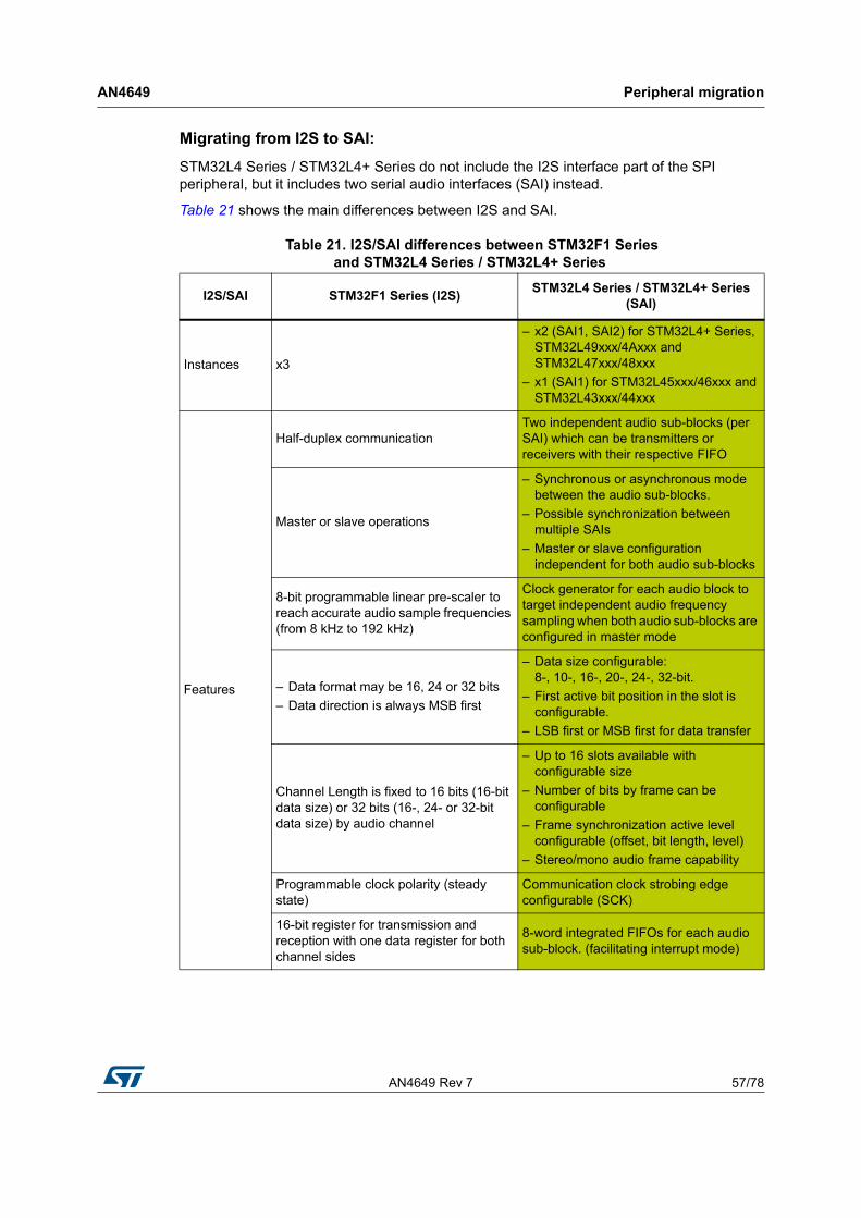
AN4649 Rev 7 57/78
AN4649 Peripheral migration
77
Migrating from I2S to SAI:
STM32L4 Series / STM32L4+ Series do not include the I2S interface part of the SPI peripheral, but it includes two serial audio interfaces (SAI) instead.
Table 21 shows the main differences between I2S and SAI.
Table 21. I2S/SAI differences between STM32F1 Seriesand STM32L4 Series / STM32L4+ Series
I2S/SAI STM32F1 Series (I2S)STM32L4 Series / STM32L4+ Series
(SAI)
Instances x3
– x2 (SAI1, SAI2) for STM32L4+ Series, STM32L49xxx/4Axxx and STM32L47xxx/48xxx
– x1 (SAI1) for STM32L45xxx/46xxx and STM32L43xxx/44xxx
Features
Half-duplex communicationTwo independent audio sub-blocks (per SAI) which can be transmitters or receivers with their respective FIFO
Master or slave operations
– Synchronous or asynchronous mode between the audio sub-blocks.
– Possible synchronization between multiple SAIs
– Master or slave configuration independent for both audio sub-blocks
8-bit programmable linear pre-scaler to reach accurate audio sample frequencies (from 8 kHz to 192 kHz)
Clock generator for each audio block to target independent audio frequency sampling when both audio sub-blocks are configured in master mode
– Data format may be 16, 24 or 32 bits
– Data direction is always MSB first
– Data size configurable: 8-, 10-, 16-, 20-, 24-, 32-bit.
– First active bit position in the slot is configurable.
– LSB first or MSB first for data transfer
Channel Length is fixed to 16 bits (16-bit data size) or 32 bits (16-, 24- or 32-bit data size) by audio channel
– Up to 16 slots available with configurable size
– Number of bits by frame can be configurable
– Frame synchronization active level configurable (offset, bit length, level)
– Stereo/mono audio frame capability
Programmable clock polarity (steady state)
Communication clock strobing edge configurable (SCK)
16-bit register for transmission and reception with one data register for both channel sides
8-word integrated FIFOs for each audio sub-block. (facilitating interrupt mode)
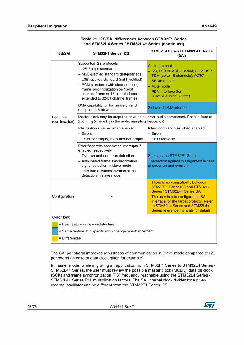
Peripheral migration AN4649
58/78 AN4649 Rev 7
The SAI peripheral improves robustness of communication in Slave mode compared to I2S peripheral (in case of data clock glitch for example)
In master mode, while migrating an application from STM32F1 Series to STM32L4 Series / STM32L4+ Series, the user must review the possible master clock (MCLK), data bit clock (SCK) and frame synchronization (FS) frequency reachable using the STM32L4 Series / STM32L4+ Series PLL multiplication factors. The SAI internal clock divider for a given external oscillator can be different from the STM32F1 Series I2S.
Features (continuation)
Supported I2S protocols:
– I2S Philips standard
– MSB-justified standard (left-justified)
– LSB-justified standard (right-justified)
– PCM standard (with short and long frame synchronization on 16-bit channel frame or 16-bit data frame extended to 32-bit channel frame)
Audio protocols:
– I2S, LSB or MSB-justified, PCM/DSP, TDM (up to 16 channels), AC’97
– SPDIF output
– Mute mode
– PDM interface (for STM32L4Rxxx/L4Sxxx)
DMA capability for transmission and reception (16-bit wide)
2-channel DMA interface
Master clock may be output to drive an external audio component. Ratio is fixed at 256 × FS (where FS is the audio sampling frequency)
Interruption sources when enabled:
– Errors
– Tx Buffer Empty, Rx Buffer not Empty
Interruption sources when enabled:
– Errors
– FIFO requests
Error flags with associated interrupts if enabled respectively
– Overrun and underrun detection
– Anticipated frame synchronization signal detection in slave mode
– Late frame synchronization signal detection in slave mode
Same as the STM32F1 Series
+ protection against misalignment in case of underrun and overrun
Configuration -
– There is no compatibility between STM32F1 Series I2S and STM32L4 Series / STM32L4+ Series SAI
– The user has to configure the SAI interface for the target protocol. Refer to STM32L4 Series and STM32L4+ Series reference manuals for details
Color key:
= New feature or new architecture
= Same feature, but specification change or enhancement
= Differences
Table 21. I2S/SAI differences between STM32F1 Seriesand STM32L4 Series / STM32L4+ Series (continued)
I2S/SAI STM32F1 Series (I2S)STM32L4 Series / STM32L4+ Series
(SAI)

AN4649 Rev 7 59/78
AN4649 Peripheral migration
77
In STM32L4 Series / STM32L4+ Series, the SAI1 and SAI2 input clocks are derived (selected by software) from one of the following sources:
• For STM32L4+ Series, STM32L49xxx/4Axxx and STM32L47xxx/48xxx:
– an external clock mapped on SAI1_EXTCLK for SAI1 and SAI2_EXTCLK for SAI2
– PLLSAI1 (P) divider output (PLLSAI1CLK)
– PLLSAI2 (P) divider output (PLLSAI2CLK)
– main PLL (P) divider output (PLLSAI3CLK)
• For STM32L45xxx/46xxx and STM32L43xxx/44xxx devices:
– an external clock mapped on SAI1_EXTCLK for SAI1
– PLLSAI1 (P) divider output (PLLSAI1CLK)
– main PLL (P) divider output (PLLSAI2CLK)
– HSI16 clock
When the clock is derived from one of the internal PLLs, the three PLL inputs are either HSI16, HSE or MSI (between 4 and 48 MHz) divided by a programmable factor PLLM (from 1 to 8 (or from 1 to 16 for STM32L4+ Series)).
For STM32L4+ Series, when the clock is derived from one of the internal PLL, the three PLL inputs are either HSI16, HSE or MSI divided by its own programmable factor (PLLM, PLLSAI1M and PLLSAI2M) (from 1 to 16).
This input is then multiplied by PLLN (from 8 to 86 (or from 8 to 127 for STM32L4+ Series)) to reach the PLL VCO frequency, which must be between 64 and 344 MHz.
It is finally divided by PLLP to provide the input clock of SAI (max. 80 MHz (or 120 MHz for STM32L4+ Series)):
• 7 or 17 on STM32L47xxx/48xxx
• [2...31] on STM32L4+ Series, STM32L49xxx/4Axxx, STM32L45xxx/46xxx and STM32L43xxx/44xxx
When the master clock MCLK is used by the external slave audio peripheral, the PLL output is divided by the SAI internal master clock divider factor (1, 2, 4, 6, 8, ..., 30) to provide the master clock (MCLK). The data bit clock is then derived from MCLK the following the formula:
Where:
• FRL is the number of bit clock cycles - 1 in the audio frame (0 to 255).
• (FRL+ 1) must be a power of 2 higher or equal to 8.
• (FRL + 1) = 8, 16, 32, 64, 128, 256.
The SCK can also be directly connected to the input clock of the SAI when MCLK output is not needed.
The frame synchronization (FS) frequency is always MCLK / 256.
SCK MCLK FRL 1+( ) 256⁄×=

Peripheral migration AN4649
60/78 AN4649 Rev 7
Figure 7 shows the clock generation scheme in the STM32L4 Series / STM32L4+ Series. Refer to the STM32L4 Series / STM32L4+ Series reference manuals for more details.
Figure 7. STM32L4 Series / STM32L4+ Series clock generation for SAI Master mode(when MCLK is required)
4.14 Cyclic redundancy check calculation unit (CRC)
The CRC is very similar in STM32F1 Series and STM32L4 Series / STM32L4+ Series.
Table 22 shows the differences.
MS39860V6
PLL(M)
SAI audio sub-block A
4 – 48MHz
80MHz max
64 – 344MHz
(N) (P)
FS_A
MCLK_A
SCK_A
÷
÷
SAI audio sub-block B
FS_B
MCLK_B
SCK_B
÷256
÷
÷[1:8]
x ÷
From external clock source
From 3 possible similar PLLs
(only on STM32L47xxx/48xxx andSTM32L49/4Axxx devices)
HSIHSEMSI [8:86] 7,17 or
[2..31]
1,2,4,6,8,10,..,30
1,2,4,6,8,10,..,30
256/[8,16,32,64,
128,256]
÷
256/[8,16,32,64,
128,256]
÷256
Table 22. CRC differences between STM32F1 Series and STM32L4 Series / STM32L4+ Series
CRC STM32F1 Series STM32L4 Series / STM32L4+ Series
Features
– Single input/output 32-bit data register
– CRC computation done in 4 AHB clock cycles (HCLK) for the 32-bit data size
– General-purpose 8-bit register (can be used for temporary storage)
– Uses CRC-32 (Ethernet) polynomial: 0x4C11DB7
– Handles 32-bit data size
– Fully programmable polynomial with programmable size (7-, 8-, 16-, 32-bit)
– Handles 8-,16-, 32-bit data size
– Programmable CRC initial value
– Input buffer to avoid bus stall during calculation
– Reversibility option on I/O data

AN4649 Rev 7 61/78
AN4649 Peripheral migration
77
4.15 Controller area network (bxCAN)
STM32L4 Series and STM32L4+ Series implement the same bxCAN as STM32F1 Series.
Configuration -
– Configuration registers on STM32F1 Series are identical on STM32L4 Series / STM32L4+ Series
– STM32L4 Series / STM32L4+ Series includes additional registers for new features
– Refer to the STM32L4 Series and STM32L4+ Series reference manuals for details
Color key:
= New feature or new architecture
Table 22. CRC differences between STM32F1 Series and STM32L4 Series / STM32L4+ Series (continued)
CRC STM32F1 Series STM32L4 Series / STM32L4+ Series
Table 23. bxCAN differences between STM32F1 Series and STM32L4 Series / STM32L4+ Series
bxCAN STM32F1 Series STM32L4 Series /S TM32L4+ Series
Instances x2 (up to)
– x1 on STM32L4+ Series, STM32L47xxx/48xxx, STM32L45xxx/46xxx and STM32L43xxx/44xxx
– x2 on STM32L49xxx/4Axxx
Features
– Supports CAN protocol version 2.0 A, B Active
– Bit rates up to 1 Mbit/s
– Supports the time triggered communication option
– Tx: 3 transmit mailboxes, configurable priority, time stamp on SOF transmission
– Rx: 2 receive FIFOs with 3 stages, scalable filter banks, identifier list, configurable FIFO overrun, time stamp on SOF reception
– Time-triggered communication option: Disable automatic retransmission mode 16-bit free running timer Time Stamp sent in last two data bytes
– Management Maskable interrupts Software-efficient mailbox mapping at a unique address space
Dual CAN (connectivity line only) Dual CAN (only on STM32L49xxx/4Axxx)

Peripheral migration AN4649
62/78 AN4649 Rev 7
4.16 USB on-the-go full-speed (USB OTG FS)
The STM32L4+ Series, STM32L49xxx/4Axxx, STM32L47xxx/48xxx, STM32F105xx and STM32F107xx devices implement very similar USB OTG FS peripherals.
The STM32L45xxx/46xxx, STM32L43xxx/44xxx, STM32L41xxx/42xxx, STM32F102xx and STM32F103xx devices implement only a USB FS device interface.
On the STM32L4+ Series, STM32L49xxx/4Axxx, STM32L45xxx/46xxx, STM32L43xxx/44xxx and STM32L41xxx/42xxx devices, a clock recovery system (CRS) block is included. It can provide a precise clock to the USB peripheral:
• When using USB device mode, the CRS allows crystal-less USB operation.
• When using USB host mode, the CRS allows low frequency crystal (32.768 kHz) USB operation.
Most features supported by STM32F1 Series are also supported by STM32L4 Series / STM32L4+ Series. Table 24 and Table 25 show the differences.
Configuration -
– Configuration registers on STM32F1 Series are identical than the ones on STM32L4 Series / STM32L4+ Series
– Refer to the STM32L4 Series and STM32L4+ Series reference manuals for details
Color key:
= Same feature, but specification change or enhancement
Table 23. bxCAN differences between STM32F1 Series and STM32L4 Series / STM32L4+ Series (continued)
bxCAN STM32F1 Series STM32L4 Series /S TM32L4+ Series

AN4649 Rev 7 63/78
AN4649 Peripheral migration
77
Table 24. USB OTG FS differences between STM32F1 Series andSTM32L4 Series/ STM32L4+ Series
USB STM32F105xx and STM32F107xx STM32L4+ Series, STM32L49xxx/4Axxx
and STM32L47xxx/48xxx
Features
– Universal Serial Bus Revision 2.0
– Full support for the USB On-The-Go (USB OTG)
FS mode:
– 1 bidirectional control endpoint
– 3 IN endpoints (Bulk, Interrupt, Isochronous)
– 3 OUT endpoints (Bulk, Interrupt, Isochronous)
FS mode:
– 1 bidirectional control endpoint
– 5 IN endpoints (Bulk, Interrupt, Isochronous)
– 5 OUT endpoints (Bulk, Interrupt, Isochronous)
USB internal connect/disconnect feature with an internal pull-up resistor on the USB D + (USB_DP) line
-
– Attach detection protocol (ADP)
– Battery charging detection (BCD)
Independent VDDUSB power supply allowing lower VDDCORE while using USB
Mapping AHB AHB2
Buffer memory– 1.25 Kbytes data FIFOs
– Management of up to 4 Tx FIFOs (1 for each IN end point) + 1 Rx FIFO.
– 1.25 Kbytes data FIFOs
– Management of up to 6 Tx FIFOs (1 for each IN end point) + 1 Rx FIFO
Low-power modes
USB suspend and resume– USB suspend and resume
– Link power management (LPM) support
Configuration -
– In STM32L4 Series / STM32L4+ Series the registers are different.
– Refer to the STM32L4 Series and STM32L4+ Series reference manuals for details.
Color key:
= New feature or new architecture
= Same feature, but specification change or enhancement
= Differences

Peripheral migration AN4649
64/78 AN4649 Rev 7
Table 25. USB FS differences between STM32F1 Series and STM32L4 Series
USB STM32F102xx and STM32F103xx STM32L45xxx/46xxx,
STM32L43xxx/44xxx and STM32L41xxx/42xxx
Features
Universal serial bus revision 2.0.Universal serial bus revision 2.0, including link power management (LPM) support
– Configurable number of endpoints from 1 to 8
– Cyclic redundancy check (CRC) generation/checking, Non-return-to-zero Inverted
(NRZI) encoding/decoding and bit-stuffing
– Isochronous transfers support
– Double-buffered bulk/isochronous endpoint support
– USB Suspend/Resume operations
– Frame locked clock pulse generation
NA
– Attach detection protocol (ADP)
– Battery charging detection (BCD)
– USB connect / disconnect capability (controllable embedded pull-up resistor on USB_DP line)
Independent VDDUSB power supply allowing lower VDDCORE while using USB
Mapping APB1 APB1
Buffer memory
– 512 bytes (endpoint buffers and buffer descriptors structure)
– Shared with bxCAN interface (cannot use both CAN and USB FS simultaneously)
1024 bytes of dedicated packet buffer memory SRAM
Low-power modes
USB suspend and resume– USB suspend and resume
– Link power management (LPM) support
Configuration -
– In STM32L4 Series the registers are different.
– Refer to the STM32L4 Series reference manuals for details.
Color key:
= New feature or new architecture
= Same feature, but specification change or enhancement
= Feature not available (NA)
= Differences

AN4649 Rev 7 65/78
AN4649 Peripheral migration
77
4.17 Flexible static memory controller (FMC/FSMC)
STM32L4 Series / STM32L4+ Series implement a flexible static memory controller (FSMC, also named FMC) which is very similar to the one in STM32F1 Series.
Table 26 shows the differences.
Table 26. FMC/FSMC differences between STM32F1 Series andSTM32L4 Series / STM32L4+ Series
FMC/FSMC STM32F1 SeriesSTM32L4 Series / STM32L4+ Series
Features
Interfaces with static memory-mapped devices including:
– Static random access memory (SRAM)
– NOR Flash memory
– PSRAM (4 memory sub-banks in bank1)
– OneNAND Flash memory
NOR Flash 8-, 16-, 32-bit SRAM and ROM 8-, 16-bit SRAM and ROM
NAND Flash
2 banks of NAND Flash (bank2, bank 3)
1 bank of NAND Flash (bank 3)
With ECC hardware checking up to 8 Kbytes of data
PC card 16-bit PC Card compatible devices NA
FIFO Write Data FIFO, 2 word long
– Write FIFO 16x32-bit length (Data + Address)
– Write FIFO can be disabled (only on STM32L4+ Series and STM32L49xxx/4Axxx)
Various
NA
– Programmable continuous clock (FMC_CLK) output for asynchronous and synchronous accesses
– Programmable data hold timing (for STM32L4Rxxx/Sxxx)
– Programmable timings (wait states, bus turnaround cycles, output enable and write enable delays, independent read and write timings)
– Burst mode access to synchronous devices (NOR Flash/PSRAM)
– 8- or 16-bit wide databus
– Translation of 32-bit AHB transaction into 16- or 8-bit accesses to external devices
– Independent Chip Select control for each memory bank
– Independent configuration for each memory bank
– Write-enable and byte lane select outputs for use with PSRAM and SRAM
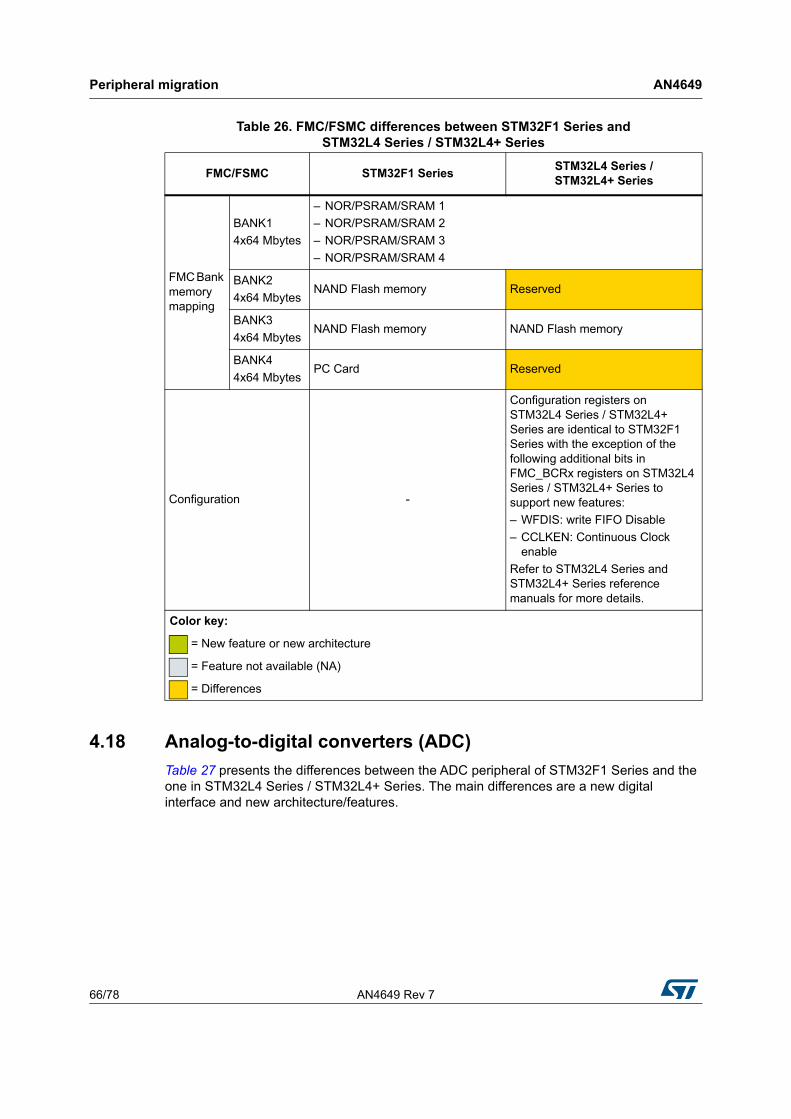
Peripheral migration AN4649
66/78 AN4649 Rev 7
4.18 Analog-to-digital converters (ADC)
Table 27 presents the differences between the ADC peripheral of STM32F1 Series and the one in STM32L4 Series / STM32L4+ Series. The main differences are a new digital interface and new architecture/features.
FMC Bank memory mapping
BANK1
4x64 Mbytes
– NOR/PSRAM/SRAM 1
– NOR/PSRAM/SRAM 2
– NOR/PSRAM/SRAM 3
– NOR/PSRAM/SRAM 4
BANK2
4x64 MbytesNAND Flash memory Reserved
BANK3
4x64 MbytesNAND Flash memory NAND Flash memory
BANK4
4x64 MbytesPC Card Reserved
Configuration -
Configuration registers on STM32L4 Series / STM32L4+ Series are identical to STM32F1 Series with the exception of the following additional bits in FMC_BCRx registers on STM32L4 Series / STM32L4+ Series to support new features:
– WFDIS: write FIFO Disable
– CCLKEN: Continuous Clock enable
Refer to STM32L4 Series and STM32L4+ Series reference manuals for more details.
Color key:
= New feature or new architecture
= Feature not available (NA)
= Differences
Table 26. FMC/FSMC differences between STM32F1 Series andSTM32L4 Series / STM32L4+ Series
FMC/FSMC STM32F1 SeriesSTM32L4 Series / STM32L4+ Series

AN4649 Rev 7 67/78
AN4649 Peripheral migration
77
Table 27. ADC differences between STM32F1 Series and STM32L4 Series / STM32L4+ Series
ADC STM32F1 Series STM32L4 Series / STM32L4+ Series(1)
ADC type SAR structure
Instances
Up to 3 instances (for STM32F103xC/D/E/F/G)
– 3 instances (STM32L49xxx/4Axxx and STM32L47xxx/48xxx)
– 2 instances (STM32L41xxx/42xxx)
– 1 instance (STM32L4+ Series, STM32L45xxx/46xxx and STM32L43xxx/44xxx)
Max sampling frequency
Up to 2 Msps in interleaved mode (for STM32F105xx and STM32f107xx)
– 5.1 Msps (Fast channels)
– 4.8 Msps (Slow channels)
Number of channels
Up to 21 channels (for STM32F103xC/D/E/F/G)
Up to 19 channels per ADC
Resolution 12-bit 12-bit + digital oversampling up to 16 bits
Conversion modes
Single / continuous / scan / discontinuous
– Single / continuous / scan / discontinuous
– Dual mode
DMA Yes
External trigger
Yes
External event for regular group:
For ADC1/ADC2:
TIM1 CC1
TIM1 CC2
TIM1 CC3
TIM2 CC2
TIM3 TRGO
TIM4 CC4
EXTI line 11
TIM8_TRGO
SWSTART
For ADC3:
TIM3_CC1
TIM2_CC3
TIM1_CC3
TIM8_CC1
TIM8_TRGO
TIM5_CC1
TIM5_CC3
SWSTART
External event for injected group:
For ADC1/ADC2:
TIM1_TRGO
TIM1_CC4
TIM2_TRGO
TIM2_CC1
TIM3_CC4
TIM4_TRGO
EXTI line 15
TIM8_CC4
For ADC3:
TIM1_CC4
TIM1_TRGO
TIM4_CC3
TIM8_CC2
TIM8_CC4
TIM5_TRGO
TIM5_CC4
JWSTART
External event for regular group:
TIM1 CC1
TIM1 CC2
TIM1 CC3
TIM2 CC2
TIM3 TRGO
TIM4 CC4
EXTI line 11 TIM8_TRGO
TIM8_TRGO2
TIM1_TRGO
TIM1_TRGO2
TIM2_TRGO
TIM4_TRGO
TIM6_TRGO
TIM15_TRGO
TIM3_CC4
External event for injected group:
TIM1 TRGO
TIM1 CC4
TIM2 TRGO
TIM2 CC1
TIM3 CC4
TIM4 TRGO
EXTI line15
TIM8_CC4
TIM1_TRGO2
TIM8_TRGO
TIM8_TRGO2
TIM3_CC3
TIM3_TRGO
TIM3_CC1
TIM6_TRGO
TIM15_TRGO
Supply requirement
2.4 V to 3.6 – 1.62 V to 3.6 V
– Independent power supply (VDDA)

Peripheral migration AN4649
68/78 AN4649 Rev 7
4.19 Digital-to analog converter (DAC)
STM32L4 Series and STM32L4+ Series implement enhanced DAC compared to the one present in STM32F1 Series.
Table 28 shows the differences.
Reference voltage
– External
– 2.4 V to VDDA
Reference voltage for STM32L4 Series / STM32L4+ Series external (1.8 V to VDDA) or internal (2.048 V or 2.5 V)
Electrical parameters
– 160 μA (Typ) on VREF DC current
– 0.8 mA (Typ) on VDDA DC currentConsumption proportional to conversion speed: 200 μA/Msps
Input range VREF- ≤ VIN ≤ VREF+ VREF- ≤ VIN ≤ VREF+
Color key:
= New feature or new architecture
= Same feature, but specification change or enhancement
1. On STM32L4 Series / STM32L4+ Series devices on which the peripheral is not implemented, the external event is not applicable.
Table 27. ADC differences between STM32F1 Series and STM32L4 Series / STM32L4+ Series (continued)
ADC STM32F1 Series STM32L4 Series / STM32L4+ Series(1)
Table 28. DAC differences between STM32F1 Series and STM32L4 Series / STM32L4+ Series
DAC STM32F1 Series STM32L4 Series / STM32L4+ Series(1)
Number of channels
x2 – x2 for STM32L4+ Series, STM32L49xxx/4Axxx,
STM32L47xxx/48xxx and STM32L43xxx/44xxx
– x1 for STM32L45xxx/46xxx
Resolution 12-bit
Features
– Left or right data alignment in 12-bit mode
– Noise-wave and triangular-wave generation
– DAC with 2 channels for independent or simultaneous conversions
NA
– Buffer offset calibration
– DAC1_OUTx can be disconnected from output pin
– Sample and hold mode for low power operation in Stop mode
DMA Yes

AN4649 Rev 7 69/78
AN4649 Peripheral migration
77
External trigger
Yes
– TIM2 TRGO
– TIM4 TRGO
– TIM5 TRGO
– TIM6 TRGO
– TIM7 TRGO
– TIM8 TRGO (TIM3 TRGO on connectivity devices(2))
– EXTI line 9
– SW TRIG
– TIM6 TRGO
– TIM8 TRGO
– TIM7 TRGO
– TIM5 TRGO
– TIM2 TRGO
– TIM4 TRGO
– EXTI line9
– SW TRIG
Additional trigger for STM32L4+ Series:
– TIM1_TRGO
– TIM15_TRGO
– LPTIM1_OUT
– LPTMI2_OUT
Supply requirement
2.4 V to 3.6 V– 1.8 V to 3.6 V
– Independent power supply (VDDA)
Reference Voltage
External
2.4 V ≤ VREF+ ≤ VDDAExternal (1.8 V to VDDA) or internal (2.048 V or 2.5 V)
Configuration - SW compatible except for output buffer management
Color key:
= New feature or new architecture
= Same feature, but specification change or enhancement
= Feature not available (NA)
= Differences
1. On STM32L4 Series /S TM32L4+ Series devices on which the peripheral is not implemented, the external trigger is not applicable
2. Connectivity = STM32F105xx and STM32F107xx lines
Table 28. DAC differences between STM32F1 Series and STM32L4 Series / STM32L4+ Series (continued)
DAC STM32F1 Series STM32L4 Series / STM32L4+ Series(1)

Software migration AN4649
70/78 AN4649 Rev 7
5 Software migration
5.1 References
Refer to the documents listed below for more details.
• The definitive guide to Arm® Cortex®-M3 and Cortex®-M4 processors
• STM32F10xxx/20xxx/21xxx/L1xxxx Cortex®-M3 programming manual (PM0056)
• STM32F3 Series, STM32F4 Series, STM32L4 Series and STM32L4+ Series Cortex®-M4 programming manual (PM0214)
• Cortex®-M3 Technical Reference Manual, available on http://infocenter.arm.com
• Cortex®-M4 Technical Reference Manual, available from http://infocenter.arm.com
5.2 Cortex®-M3 and Cortex®-M4 overview
5.2.1 STM32 Cortex®-M3 processor and core peripherals
The Cortex®-M3 processor is built on a high-performance processor core, with a 3-stage pipeline Harvard architecture, making it ideal for demanding embedded applications. The processor delivers an exceptional power efficiency through an efficient instruction set and extensively optimized design. The Cortex®-M3 provides a high-end processing hardware including single-cycle 32x32 multiplications and a dedicated hardware division.
Cortex®-M3 proce•Tight integration of system peripherals reducing the area and development costs
• Thumb instruction set combining a high code density with 32-bit performance
• Code-patch ability for ROM system update
• Power control optimization of system components
• Integrated sleep modes for a low-power consumption
• Fast code execution permitting a slower processor clock or increasing the sleep mode time
• Hardware division and fast multiplier
• Deterministic, high-performance interrupt handling for time-critical applications
• Extensive debug and trace capabilities.

AN4649 Rev 7 71/78
AN4649 Software migration
77
Figure 8 represents the STM32 Cortex®-M3 implementation.
Figure 8. STM32 Cortex®-M3 implementation
Cortex®-M3 key features
• Architecture 32 bits RISC ARMv7-M.
• 3-stage pipeline with branch speculation
• Instruction set:
– Thumb, Thumb-2
– Hardware multiply, hardware divide, saturated arithmetic
5.2.2 STM32 Cortex®-M4 processor and core peripherals
The Cortex®-M4 processor is a high performance 32-bit processor designed for the microcontroller market. It offers significant benefits to the developers, including:
• Outstanding processing performance combined with fast interrupt handling
• Enhanced system debug with extensive breakpoint and trace capabilities
• Efficient processor core, system and memories
• Ultra-low power consumption with integrated sleep modes
• Platform security robustness, with integrated memory protection unit (MPU).
The Cortex®-M4 processor is built on a high-performance processor core, with a 3-stage pipeline Harvard architecture, making it ideal for demanding embedded applications. The processor delivers an exceptional power efficiency through an efficient instruction set and extensively optimized design, providing high-end processing hardware including IEEE754- compliant single-precision floating-point computation, a range of single-cycle and SIMD multiplication and multiply-with-accumulate capabilities, a saturating arithmetic and dedicated hardware division.
MSv43981V1
Embedded trace macrocellNVIC
Debug access
port
Serial wire
viewer
Bus matrixCode
interfaceSRAM and
peripheral interface
Data watchpoints
Flashpatch
Cortex-M3 processor
Processorcore

Software migration AN4649
72/78 AN4649 Rev 7
Figure 9 represents the STM32 Cortex®-M4 implementation.
Figure 9. STM32 Cortex®-M4 implementation
Cortex®-M4 key features
• Architecture 32 bits RISC ARMv7E-M.
• 3-stage pipeline with branch speculation
• Instruction set:
– Thumb, Thumb-2
– Hardware multiply, Hardware divide, saturated arithmetic
– DSP extensions:
- Single cycle 16/32-bit MAC
- Single cycle dual 16-bit MAC
- 8/16-bit SIMD arithmetic.
– FPU (VFPv4-SP)
5.2.3 Software point of view
In addition to the Cortex®-M3, the Cortex®-M4 provides:
• SIMD, or Single Instruction Multiple Data, operations
• Additional fast MAC and multiply instructions
• Saturating arithmetic instructions
• Single precision FPU (floating point unit) instructions.
MSv41070V1
Embedded Trace
MacrocellTM
NVIC
Debug access
port
Memoryprotection unit
Serial wire
viewer
Bus matrixCode
interfaceSRAM and
peripheral interface
Data watchpoints
Flashpatch
Cortex-M4 processor FPU
Processorcore

AN4649 Rev 7 73/78
AN4649 Software migration
77
This means on software point of view, the Cortex®-M3 software can be run on the Cortex®-M4.
To improve and speed-up the STM32F1 Series software on the new STM32L4 platforms, the developer needs to switch on the FPU. This can be done on makefile side or using software development tools:
• On Keil® µVision®
– On “Project” open “Option for Target”
– Go to “Target”...“Code Generation”
– Set “Floating Point Hardware” to “Use Single Precision”
• On IAR Systems®
– On “Project” open “Options...”
– Go to “General Options”...“Target”
– Set “Floating point settings”, ‘FPU” to “VFPv4 single precision”

Software migration AN4649
74/78 AN4649 Rev 7
5.3 Cortex mapping overview
Except the FPU, the mapping is similar on the Cortex®-M3 and the Cortex®-M4.
Table 29. Cortex overview mapping for STM32F1 Series and STM32L4 Series / STM32L4+ Series
STM32F1 SeriesSTM32L4 Series / STM32L4+ Series
Core
Architecture Cortex®-M3 Cortex®-M4
Nested vectored interrupt controller (NVIC)
68 maskable interrupt channels
Maskable interrupt channel:
– 94 (STM32L4+ Series)
– 91 (STM32L49xxx/4Axxx)
– 82 (STM32L47xxx/48xxx)
– 67 (STM32L45xxx/46xxx, STM32L43xxx/44xxx and STM32L41xxx/42xxx)
Extended interrupts and
events controller (EXTI)
Up to 20 event/interrupt
– Up to 41 event/interrupt (STM32L4+ Series and STM32L49xxx/4Axxx)
– Up to 40 event/interrupt (STM32L47xxx/48xxx)
– Up to 37 event/interrupt (STM32L45xxx/46xxx, STM32L43xxx/44xxx and STM32L41xxx/42xxx)
Mapping
System timer 0xE000E010-0xE000E01F 0xE000E010-0xE000E01F
Nested vectored interrupt controller
0xE000E100-0xE000E4EF 0xE000E100-0xE000E4EF
System control block 0xE000ED00-0xE000ED3F 0xE000ED00-0xE000ED3F
Floating point unit coprocessor access control
NA 0xE000ED88-0xE000ED8B
Memory protection unit 0xE000ED90-0xE000EDB8 0xE000ED90-0xE000EDB8
Nested vectored interrupt controller
0xE000EF00-0xE000EF03 0xE000EF00-0xE000EF03
Floating point unit NA 0xE000EF30-0xE000EF44

AN4649 Rev 7 75/78
AN4649 Revision history
77
6 Revision history
Table 30. Document revision history
Date Revision Changes
11-Jun-2015 1 Initial release.
23-Nov-2015 2
Section: Memory mapping updated: Stop 0 mode added for content preservation
Table: PWR differences between STM32F1 Series and STM32L4 Series updated: Stop 0 mode added
10-Mar-2016 3Section 1: STM32L4 Series overview: added category 2 and 4 for STLM32L4.
20-Feb-2017 4
Updated:
– Document title.
– Introduction: STM32L4 Series reference manuals.
– Section 1: STM32L4 Series / STM32L4+ Series overview.
– Cat. 2 devices replaced by STM32L49xxx/4Axxx and STM32L47xxx/48xxx devices.
– Cat. 4 devices replaced bySTM32L45xxx/46xxx and STM32L43xxx/44xxx devices.
– Section 2: Hardware migration: Table 1 and SMPS data.
– Table 6, Table 7, Table 8, Table 9, Table 10, Table 11, Table 14, Table 16, Table 19, Table 20, Table 24, Table 27, Table 28.
– Section 4.5.3: Peripheral clock configuration.
– Section 4.16: USB on-the-go full-speed (USB OTG FS): added description of clock recovery system block.
– Figure 7.
Added:
– Section 4.17: Flexible static memory controller (FMC/FSMC).
– Section 5: Software migration.
Removed Table Product category overview.
01-Sep-2017 5Updated the whole document to add the information about STM32L4+ Series devices.

Revision history AN4649
76/78 AN4649 Rev 7
11-Apr-2018 6
Updated:
– Table 6: Bootloader interfaces on STM32F1 and STM32L4 Series / STM32L4+ Series
– DAC naming: 1 DAC with 2 channels instead of 2 DACs
Table 30. Document revision history (continued)
Date Revision Changes

AN4649 Rev 7 77/78
AN4649 Revision history
77
18-Sep-2018 7
Added:
– Information related to STM32L41xxx/42xxx to the whole document
Updated:
– Cover page
– Section 1: STM32L4 Series / STM32L4+ Series overview
– Section 2: Hardware migration
– Section 3: Boot mode selection
– Section 4.2: Memory mapping
– Section 4.9: Extended interrupts and events controller (EXTI) source selection
– Section 4.16: USB on-the-go full-speed (USB OTG FS)
– Section 5.1: References
– Section 4.5.3: Peripheral clock configuration
– Recommendations to migrate from the STM32F1 Series board to the STM32L4 Series / STM32L4+ Series board on page 14
– SMPS packages on page 17
– Table 1: Packages available on STM32L4 Series and STM32L4+ Series
– Table 2: Pinout differences between STM32F1 Series and STM32L4 Series / STM32L4+ Series (QFP)
– Table 5: Boot modes for STM32L4+ Series, STM32L49xxx/4Axxx, STM32L45xxx/46xxx, STM32L43xxx/44xxx and STM32L41xxx/42xxx devices
– Table 6: Bootloader interfaces on STM32F1 and STM32L4 Series / STM32L4+ Series
– Table 7: Peripheral compatibility analysis between STM32F1 Series and STM32L4 Series / STM32L4+ Series
– Table 10: Interrupt vector differences between STM32F1 Series and STM32L4 Series / STM32L4+ Series
– Table 11: RCC differences between STM32F1 Series and STM32L4 Series / STM32L4+ Series
– Table 14: PWR differences between STM32F1 Series and STM32L4 Series / STM32L4+ Series
– Table 17: Flash differences between STM32F1 Series and STM32L4 Series / STM32L4+ Series
– Table 19: I2C differences between STM32F1 Series and STM32L4 Series / STM32L4+ Series
– Table 20: SPI differences between STM32F1 Series and STM32L4 Series / STM32L4+ Series
– Table 25: USB FS differences between STM32F1 Series and STM32L4 Series
– Table 27: ADC differences between STM32F1 Series and STM32L4 Series / STM32L4+ Series
– Table 29: Cortex overview mapping for STM32F1 Series and STM32L4 Series / STM32L4+ Series
Table 30. Document revision history (continued)
Date Revision Changes

AN4649
78/78 AN4649 Rev 7
IMPORTANT NOTICE – PLEASE READ CAREFULLY
STMicroelectronics NV and its subsidiaries (“ST”) reserve the right to make changes, corrections, enhancements, modifications, and improvements to ST products and/or to this document at any time without notice. Purchasers should obtain the latest relevant information on ST products before placing orders. ST products are sold pursuant to ST’s terms and conditions of sale in place at the time of order acknowledgement.
Purchasers are solely responsible for the choice, selection, and use of ST products and ST assumes no liability for application assistance or the design of Purchasers’ products.
No license, express or implied, to any intellectual property right is granted by ST herein.
Resale of ST products with provisions different from the information set forth herein shall void any warranty granted by ST for such product.
ST and the ST logo are trademarks of ST. All other product or service names are the property of their respective owners.
Information in this document supersedes and replaces information previously supplied in any prior versions of this document.
© 2018 STMicroelectronics – All rights reserved