Embed Size (px)
Citation preview

Freescale Semiconductor Document Number: AN4705 Application Note Rev. 0, 03/2013
© Freescale Semiconductor, Inc., 2013 _______________________________________________________________________
Low-Power Wireless Charger Transmitter Design Using MC56F8006 DSC by: Xiang Gao
1 Introduction Wireless power transmission system transfers electrical power from transmitter to receiver without any wire connection. Due to safety, freedom, reliable, convenient and long life, wireless charging is popular, and widely used in everything such as toothbrushes, LED candles, remote controls, medical equipment, mobile phones, and other equipment. This paper describes a Freescale low-power wireless transmitter solution (TX) compliant to the “Qi” standard of the Wireless Power Consortium (WPC), using single-stage full-bridge resonant inverter topology on Freescale ultra low cost MC56F8006 DSC device.
This application note focuses on cost-effective, flexible and high integrated platform to show significant features of low-power wireless transmitter such as wide DC input voltage range of 5–16 V with single power stage, free positioning with multiple primary coils, simple and robust communication demodulation circuit, low-power standby operation, precise
Contents 1 Introduction ..................................................................... 1
2 MC56F8006 DSC Advantages and Features ................... 2
3 Target Control Theory ..................................................... 3
3.1 Full-bridge Inverter with Resonant Network .......... 3
3.2 Phase-Shifted PWM Control Theory ...................... 4
4 System Design Concept ................................................... 5
4.1 System configuration .............................................. 5
4.2 System specification ............................................... 7
5 Hardware Design ............................................................. 7
5.1 MC56F8006 Resource Design ................................ 8
5.2 Power Stage Design ................................................ 9
5.3 Pre-Driver Circuits Design .................................... 14
5.4 Sensing Circuits Design ........................................ 14
5.5 Communication Demodulation Circuits Design ... 14
5.6 Auxiliary Power Supply Design ............................ 15
6 Software Design ............................................................ 16
6.1 System Software Organization .............................. 16
6.2 Main Module Design ............................................ 17
6.3 ISR Design ............................................................ 20

Low-Power Wireless Charger Transmitter Design Using MC56F8006 DSC, Rev.0, 03/2013 2 Freescale Semiconductor, Inc.
and reliable power transfer with digital PID close-loop control, interoperable operation with any receiver device with WPC “Qi” logo, and user-friendly interface.
This application is also an open source based solution, which gives design freedom to the customers, allowing product differentiation, and providing access to essential Freescale wireless charging embedded software libraries.
2 MC56F8006 DSC advantages and features The MC56F8006 combines the processing power of a digital signal processor (DSP) and the functionality of a microcontroller unit (MCU) with a set of flexible peripherals on a single chip to create low-cost and high performance/price solutions.
The MC56F8006 uses the 56800E core, which is based on a dual Harvard-style architecture consisting of three execution units operating in parallel. This allows as many as six operations per instruction cycle. The MCU-style programming model and optimized instruction set allow straightforward generation of efficient, compact DSP and control code. The instruction set is also highly efficient for C compilers to enable rapid development of optimized control applications.
Because of its low cost, and flexible peripherals configuration, MC56F8006 is well-suited for many cost-effective and low power consumption applications such as digital switching mode power supplies, motor control, medical devices, power metering, handheld tools, and wireless chargers, among others.
The MC56F8006 provides the following peripherals: • One six-channel output Pulse Width Modulator (PWM) with up to 96 MHz operating clock,
three current sense inputs, and up to four fault inputs; fault tolerant design with dead time insertion, supporting both center- and edge-aligned modes
• Two Analog-to-Digital Converters (ADCs), supporting two simultaneous conversions and ping-pong conversion with dual 24 inputs, 8-, 10- and 12-bit output format, and low-power operation. The ADC can be synchronized by PWM module and a temperature sensor is integrated with each ADC.
• Two Programmable Gain Amplifiers (PGA) with programmable gain up to a maximum of 32, supporting conversion of analog signals from differential to single-ended. The starting point of PGA can be synchronized with PWM, and the PGA has the calibration features of both offset and gain.
• Two 16-bit General-Purpose Timers (GPT) with up to 96 MHz operating clock, supporting up to 12 operating modes
• One Programmable Delay Block (PDB), providing precise control of PGA/ADC and HSCMP sample time relative to PWM synchronization output
• One Periodic Interrupt Timer (PIT) for timing; one Real-Time Counter (RTC), supporting real-time clock and waking up core from low power mode
• Three High-Speed Comparators (HSCMP), supporting sample, window and digital filter • One Serial Communication Interface (SCI) with up to 6 Mbit/s baud rate, supporting full-duplex,
single-wire and LIN slave modes
Low-Power Wireless Charger Transmitter Design Using MC56F8006 DSC, Rev.0, 03/2013 Freescale Semiconductor, Inc.
• One Serial Peripheral Interface (SPI), supporting full-duplex operation, programmable length transactions from 2 to 16 and 12 master mode frequencies
• One Inter-Integrated Circuit (IIC) , supporting 10-bit address extension, general call recognition and SMBus specification
• Power Management Controller (PMC), supporting 7 power modes including ultra low power mode—Partial Power Down mode
• Computer Operating Properly (COP) timer with independent 1 kHz on-chip oscillator, supporting operation in low-power mode
• Up to 40 General-Purpose Input Output (GPIO) lines • Two internal Voltage Regulator (VR) for core and clock; internal Power-On Reset (POR) circuit
and Low Voltage Interrupt (LVI) module • Software-programmable Phase-Locked Loop (PLL) • JTAG/Enhanced On-Chip Emulation (EOnCE) for real-time debugging • Cost-effective memory configuration (16 KB Program Flash, 2 KB Program Dual-port RAM)
The low power wireless transmitter system benefits greatly from the powerful 56800E DSC CPU, on-chip clock synthesis, interrupt controller, flexible PWM module, PDB/PGA/ADC, GPT module, RTC module and GPIO module.
3 Target control theory
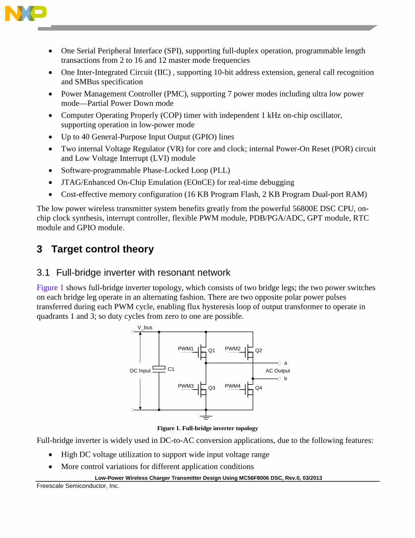
3.1 Full-bridge inverter with resonant network Figure 1 shows full-bridge inverter topology, which consists of two bridge legs; the two power switches on each bridge leg operate in an alternating fashion. There are two opposite polar power pulses transferred during each PWM cycle, enabling flux hysteresis loop of output transformer to operate in quadrants 1 and 3; so duty cycles from zero to one are possible.
Q1 Q2
Q3 Q4
C1DC Input
PWM4
PWM1 PWM2
PWM3
AC Output
V_bus
a
b
Figure 1. Full-bridge inverter topology
Full-bridge inverter is widely used in DC-to-AC conversion applications, due to the following features:
• High DC voltage utilization to support wide input voltage range • More control variations for different application conditions

Low-Power Wireless Charger Transmitter Design Using MC56F8006 DSC, Rev.0, 03/2013 4 Freescale Semiconductor, Inc.
• Unipolar fixed-frequency PWM control to reduce EMI • Phase-shifted control strategy for possible soft switching operation to improve system efficiency • Small power component stresses for medium/high power applications • Simple inverter topology with output transformer
Resonant network is used to convert AC square wave to sinusoidal wave, which is targeted to assist the converters to operate in soft switching mode, and reduce EMI from power switches in converter. The output transformer fed with sinusoidal wave will also improve power transfer efficiency and reduce harmonic radiation from the transformer side.
The transmitter reference solution targets the wide input voltage range support, high-power transfer efficiency, and low EMI. So, the single-stage full-bridge inverter with parallel LCL resonant network (shown in Figure 2) is used as power stage of transmitter to meet the specifications.
Lm
CrCoil
Lp
Inverter Output
b
a
Figure 2. Parallel LCL resonant network
3.2 Phase-shifted PWM control theory
PWM1
PWM3
PWM4
PWM2
V_ab
+V_bus
-V_bus
dead time α
Figure 3. Phase-shifted PWM principle
As Figure 3 shows, the two PWMs for one bridge leg are 180° complementary pair, and in order to prevent shoot through, a dead time (period of no power switch being “on”) must be inserted between each power switch transition. The phase difference between the PWMs of two bridge legs is called phase-shifted angle (α). The output-to-input transfer function is proportional to the phase-shifted angle.

Low-Power Wireless Charger Transmitter Design Using MC56F8006 DSC, Rev.0, 03/2013 Freescale Semiconductor, Inc.
As a result, the pulse width of the output voltage can be adjusted through changing the phase-shifted angle.
The phase-shifted PWM control has some advantages over the traditional PWM control on full-bridge inverter topology:
• Unipolar fixed-frequency PWM control to reduce system EMI • Easily implement ZVS soft switching operation to improve system efficiency • No voltage floating problem to improve system stability • 50% turn-on operation to extend the life cycle of power switch and improve system reliability
In order to meet the specification requirements, the phase-shifted PWM strategy is used in transmitter reference solution.
4 System design concept
4.1 System configuration Figure 4 shows the complete wireless charging system proposed by Freescale. It contains PC (monitoring, controlling and programming purpose), JTAG converter with isolator (connection tool between target and PC), wall adapter (or DC source, powering wireless transmitter), Freescale low-power wireless transmitter, and any receiver device which is compliant to the Qi standard.
When powering up, the transmitter system stays in standby mode for lowest power consumption. If any Qi-compliant receiver device is present on charging area of the transmitter, the transmitter will ping, locate, identify, and configure the receiver device. After successfully configuring the receiver device, the transmitter will transfer required power to the receiver. During all these phases, communication between transmitter and receiver is necessary to ensure that the system is working properly. The transmitter will terminate power transfer if the receiver device is taken away, the charging ends, or a fault occurs.
JTAG Connector + Isolator
Freescale Low Power Wireless Transmitter
Adapter Receiver Device with
“Qi” logo
Figure 4. Freescale wireless charging system configuration
This application note focuses on Freescale low-power wireless transmitter reference design. As the Figure 5 shows, transmitter system consists of the following key components:

Low-Power Wireless Charger Transmitter Design Using MC56F8006 DSC, Rev.0, 03/2013 6 Freescale Semiconductor, Inc.
• Freescale MC56F8006 DSC—this is like CPU of the system used for real-time precise control of the amount of power transferred from transmitter to receiver, communication data received, system state machine maintenance, fault monitor and protection, and HMI interaction.
• Single-stage full-bridge inverter—this is the power stage of the system which is used to convert DC power to AC square wave power.
• Resonant matching network—includes matching inductor and resonant capacitor to generate AC sinusoidal wave current on primary coil
• Primary coil array—includes seven primary coils for supporting free positioning, and transmitting power through the generated magnetic field
• Primary coil/resonant capacitors switches—the users can select proper primary coils and resonant capacitors for highly efficient power transfer according to the receiver position.
• Sensing circuits—these circuits sense the input voltage/current and coil voltage/current for power transfer control, power calculation, and fault protection.
• Pre-driver circuit—this circuit amplifies the PWM signal to drive high-power switch. • Communication demodulation circuit—this circuit is used for demodulating communication
signals from power line for linking with the receiver. • Auxiliary power supply—it generates low-voltage DC power supply for active components on
board from input. • HMI—it is used for monitoring, controlling, indicating, and debugging purpose.
Single-stage full-bridge Inverter
DC input Matching Network
Primary Coil Array
MC56F8006
Capacitance switches
Coil switches
Pre-driver circuit
Auxiliary power supply
Input sensing circuits
Coil sensing/communication demodulation
circuits
Freescale IC
HMI
Figure 5. Block diagram of Freescale low-power wireless transmitter reference solution
The actual component layout of Freescale low-power wireless transmitter platform is shown in Figure 6 for better understanding the transmitter system.

Low-Power Wireless Charger Transmitter Design Using MC56F8006 DSC, Rev.0, 03/2013 Freescale Semiconductor, Inc.
Figure 6. Real object layout of Freescale low-power wireless transmitter
4.2 System specification The transmitter reference solution operates with wide DC input voltage, and transfers enough power to meet 5 W (5V/1A) load requirement. The key system parameters are listed as follows:
• Transfer efficiency: maximum 60% • Input voltage: 5–16 V DC • Output power: up to 5 W • Standby current: < 30 mA • Operation frequency: 108 kHz • Communication baud rate: 2 kbit/s • Power stage topology: full-bridge
• And the control algorithm of transmitter includes: • WPC “Qi” communication protocol • Free position control • Output current closed-loop control—PID regulation • Current limitation • Fault protection • Safety functions, such as metal object detection
5 Hardware design Freescale wireless charger transmitter has selected digital signal controller (DSC) MC56F8006 as the control

Low-Power Wireless Charger Transmitter Design Using MC56F8006 DSC, Rev.0, 03/2013 8 Freescale Semiconductor, Inc.
core, use full bridge topology to invert the input DC voltage to high-frequency sinusoidal voltage on the primary coil. In this section, detailed hardware design will be introduced, including the following parts:
• MC56F8006 resource design • Power stage design • Pre-driver circuit design • Sensing circuits design • Communication demodulation circuit design • Auxiliary DC power supply design
Figure 7. Hardware system configuration
The application hardware system configuration is shown in Figure 7.
5.1 MC56F8006 resource design The digital signal controller (DSC) MC56F8006, is the core of the whole system which measures all the required analog quantities (input voltage, input current, primary coil voltage, and primary coil current), controls the power switches (MOSFETs) in accordance with the control algorithm, demodulates the communication signals from the receiver, and provides the main working status information via two LEDs on the PCB board.
Table 1. Functional description of MC56F8006 DSC peripherals
Peripherals Function Description RTC Real-time counter (RTC) is used for timing; to generate millisecond (ms),
second, minute, and hour time base for the charging sequence PWM • PWM0–PWM4 are used to drive full-bridge inverter.
• Fault0 and Fault1 are used to provide hardware protect function when input current or coil current is over threshold.

Low-Power Wireless Charger Transmitter Design Using MC56F8006 DSC, Rev.0, 03/2013 Freescale Semiconductor, Inc.
ADC • ANB4 is for sampling input current; ANB6 is for sampling input voltage.
• ANA7 is for sampling input voltage; ANA9 is for sampling coil current.
PDB PDB is for triggering ADC to work in Ping-Pong mode. GPIO • GPIOA4–GPIOA6 and GPIOB0–GPIOB3 are used to control coil
selection circuit. • GPIOB6 and GPIOC4 are used to control LED1 and LED2 to
indicate the working status of the system. • GPIOB7 detects the Start button. • GPIOF0 is used to control the additional capacitor when two or three
coils are selected. • GPIOD0 is used for fault enable, if necessary.
Dual Timer • TMR0 is to generate 200 µs interrupt for PID control. • TMR1 is used for receiving and processing the communication data from
receiver by its capture function.
JTAG TDI/TDO/TCK/TMS/RESET is used to connect with JTAG interface for downloading program and FreeMASTER online debugging.
5.2 Power stage design
5.2.1 Full-bridge inverter design Figure 8 shows the schematic of a full-bridge inverter used by the wireless charger transmitter. The allowed input voltage range is 4.5–19.5 V and the input current is from 0–2 A (maximum at 5 V input). LCL resonant circuit is connected to middle point of bridge leg 1 and middle point of bridge leg 2. N-channel MOSFETs of Q301–Q304 are controlled by PWMs generated from DSC. The switching frequency of PWMs is set to 108 kHz. In order to meet the above criteria, NTR4503N from On Semiconductor is selected as the main power switch. NTR4503N is 30 V, 2.5 A, single N-channel power MOSFET.

Low-Power Wireless Charger Transmitter Design Using MC56F8006 DSC, Rev.0, 03/2013 10 Freescale Semiconductor, Inc.
Input Voltage (
Figure 8. Schematic of full-bridge inverter
5.2.2 Resonant network design Resonant network is shown in Figure 9. Transmitter solution uses a multiplexer to select the position of the active area. The multiplexer shall configure the primary coil array in such a way that one, two, or three primary coils are connected in parallel to the resonant network circuit. The connected primary coils together constitute a primary cell.
Figure 9. Simplified schematic of resonant network circuit

Low-Power Wireless Charger Transmitter Design Using MC56F8006 DSC, Rev.0, 03/2013 Freescale Semiconductor, Inc.
Coil4
Coil3
Coil5
Coil2
Coil6
Coil1
Coil7
Figure 10. Primary coils composition
Transmitter primary coil array is distributed in three layers. Figure 10 shows a top view of the primary coil array. Coil4 is distributed in the first layer; Coil1, Coil3, and Coil6 are distributed in the second layer; Coil2, Coil5, and Coil7 are distributed in the third layer. Due to coil selection strategy, one, two or three coils may be selected to obtain maximum transfer efficiency. In addition, only one coil of each layer can be selected at a time.
Figure 11 shows three different coil configurations consisting of one, two, and three coils. The coils with red border are selected and the receiver is put in the area with the shade of red.
One Coil Two Coils Three Coils
Coil2 selected Coil2 ,Coil3 selected Coil1, Coil2 ,Coil4
selected
Figure 11. Primary coil selection example
With the operating frequency 109 kHz, the assembly of primary coil array and shielding has an inductance of 8.1 µH for each individual primary coil in the first layer, 8.7 µH for each individual primary coil in the second layer, and 9.6 µH for each individual primary coil in the third layer.

Low-Power Wireless Charger Transmitter Design Using MC56F8006 DSC, Rev.0, 03/2013 12 Freescale Semiconductor, Inc.
Figure 12. Schematic of coils selection circuit
Coil selection circuit is a switch, and its function is to access the corresponding coil to resonant network. Figure 12 shows one out of the seven coil selection circuits; the control signal is from DSC GPIO and the supply voltage is VSEL (12 V) generated from 5 V.
Figure 13. Schematic of matching inductor and resonant circuit
As shown in Figure 13, the impedance matching circuit is composed of L301, C307–C309, and C310–C311. The circuit in dashed box is the switch of additional resonant capacitors, which is similar to coil selection switch and will be discussed later. In order to analyze the impedance matching circuit, Figure 13 can be simplified as shown in Figure 9.
In Figure 9, mL represents matching inductance, 1mC represents resonant capacitance, 23mC represents additional resonant capacitance for multicoil configuration, and pL represents inductance of primary coils selected.
231 mmm CCC +=

Low-Power Wireless Charger Transmitter Design Using MC56F8006 DSC, Rev.0, 03/2013 Freescale Semiconductor, Inc.
pL and 23mC are connected in parallel; when the input source angular frequency of ω is low, it displays the characteristics of an inductor. As the angular frequency increases, parallel resonance occurs at a certain angular frequency of 1ω . When 1ωω > , the parallel proportion of the circuit performs capacitor character, series resonance occurs at a certain angular frequency 2ω between mL and the parallel proportion. The equivalent impedance can be calculated using the equation given below.
1)(
1
)1()(
2
3
−
+−=
++=
mp
pmmpm
mp
mp
m
CLLLCLL
j
CjLj
CjLj
LjZ
ωωω
ωω
ωω
ωω
When the numerator = 0, serial resonance occurs.
0)(232 =+− pmmpm LLCLL ωω
mpm
pm
CLLLL +
=2ω
When the denominator = 0, parallel resonance occurs.
0121 =−mpCLω
mpCL1
1 =ω
The parameters of matching inductor, capacitor, and primary coils are shown in Table 2. The gap between primary coil on layer3 and secondary coil is larger than the one on layer2 and layer1, the inductance of primary coil on layer3 is larger than that of layer2 and layer1.
Table 2. Parameters of resonant network components
Lm 3.8 µH
Cm1 300 nF
Cm23 200 nF
Lp_layer 1 8.1 µH
Lp_layer 2 8.85 µH

Low-Power Wireless Charger Transmitter Design Using MC56F8006 DSC, Rev.0, 03/2013 14 Freescale Semiconductor, Inc.
Lp_layer 3 9.62 µH
The system operating frequency of F0 = 108 kHz is selected; the additional capacitor Cm23 is chosen to make the resonant network work near the parallel resonant frequency. Increasing the value of resonant capacitor could reduce the serial resonant frequency and get a higher resonant voltage at F0 operating point.
5.3 Pre-driver circuit design The transmitter uses MC74VHC1GT125 and MAX15054 for high-side MOSFETs driver and LM5110-1M for low-side MOSFETs driver.
The features of the pre-driver circuits are listed below.
• Supports low-voltage power supply down to 4.5 V • Very short propagation delay from input to output (less than 25 ns) • Four channels PWM can be controlled by DSC independently. • Adjustable dead time
5.4 Sensing circuit design Transmitter solution needs to sample necessary signals to complete the function of system control, fault protection, and power calculation. Input voltage, input current, coil voltage, and coil current are sensed in current design.
Allegro ACS716-6BB is selected for current sensing in transmitter. ACS716 is a 120 kHz bandwidth, high-voltage isolation current sensor with integrated overcurrent detection. ACS716 sensor provides economical and precise means for current sensing applications in industrial, commercial, and communications systems.
5.5 Communication demodulation circuit design The power receiver communicates to power transmitter using backscatter modulation. The function of communication demodulation circuit is to detect the 2 kHz communication signal from the 108 kHz power signal.
Voltage Scale Down
Rectify & DC Filter Low Pass Filter Electric Level
Comparator
Communication Wave Voltage
Divider
Coil Voltage DSC
Figure 14. Block diagram of communication demodulation circuit
Figure 14 shows the block diagram of communication demodulation circuit, where the primary coil voltage serves as the input and the output is communication data following bit encoding scheme. The circuit can be divided into five parts, including voltage scale down part, rectify and DC filter part, low-pass filter part, electric level comparator part, and communication wave voltage divider part.

Low-Power Wireless Charger Transmitter Design Using MC56F8006 DSC, Rev.0, 03/2013 Freescale Semiconductor, Inc.
• Voltage scale down part:
o Scales down the voltage Coil_in to ground and Coil_Out to ground
o Adjusts the midpoint of the signal to 2.5 V and amplifies it between 0–5 V • Rectify and DC filter part:
o Rectifies the signal and converts the sinusoidal wave signal to saw tooth wave signal
o Filters the DC part of the signal and shifts the sawtooth wave signal with the middle point of 2.5 V
• Low-pass filter (LPF): Figure 15 shows the schematic of improved second-order low pass filter selected in the design.
Figure 15. Improved second-order low-pass filter
• Comparator part:
o Compares the signal value with reference to get a square wave signal • Voltage divider part:
o Reduces the amplitude of square wave signal to 3.3 V to meet DSC input port specification
5.6 Auxiliary power supply design The auxiliary power supply provides supply voltages for control, sense, communication, and driving circuits. In transmitter design, +3.3 V is needed for DSC power supply, +5 V is needed for operational amplifier, driving circuits and communication demodulation circuits, and +12 V is needed for primary coil/resonant capacitor selection circuit.

Low-Power Wireless Charger Transmitter Design Using MC56F8006 DSC, Rev.0, 03/2013 16 Freescale Semiconductor, Inc.
6 Software design
6.1 System software organization The wireless power transmitter software follows and implements WPC “Qi” 1.0.2 specification. Its main functions are object detection, multi-coil selection, communication, and output power adjustment. Some of the other functions include power saving, system monitor, fault protection, and user indication.
The software system has the following four layers.
• User layer (configuration interface)
• Application layer (communication and control)
• Middle layer (“Qi” packets receiving and PID control)
• Low layer (I/O driver and interrupt)
The system is driven to run by input communication packets and timer interrupts.
Monitor , detection, and power control
Qi PacketsReceiving
Timer-1(Bit capture)
ADC (Driven by PDB)
GPIO Timer-0(PWM control)
Communication data
Current/voltage sensing
Coil and capselection, LED
Full BridgeControl
Low Layer(HW driver)
Mid Layer
App Layer
User Interface (parameter and confirguration)
PID
User Layer
RTC(System
1ms timer)
Figure 16. Transmitter software structure
The system runs in the following five states including Idle, Detection, Localization, Charging, and Middle.
• Idle state: In this state, there is no charging activity and the DSC is in low-power mode. • Object detection: The system leaves Idle state for object detection when Start button is pressed in
the button mode. In non-button mode, the system runs detection every fixed time. • Object localization: If an object is detected, the system localizes the secondary coil and selects
suitable primary coils for powering. • Charging state: After object localization is done, the system enters the Charging state.

Low-Power Wireless Charger Transmitter Design Using MC56F8006 DSC, Rev.0, 03/2013 Freescale Semiconductor, Inc.
• Middle state: The system enters this state when failure occurs during charging or detection phase. This state decides the next state of the system depending on failure counts and detection timer.
6.2 Main module design
6.2.1 System state machine Before charging setup, the system runs through Idle, Object Detection and Localization states. See Figure 17.
• In Start Button mode, if the system staying in detection state exceeds for a certain time, then the system enters Idle state. The system wakes up when the Start button is pressed.
• In Non-Button mode, the system always runs detection until power transfer is setup. For object detection, there are two ping methods of analog ping and digital ping. If no object is found after several seconds of analog ping, then a digital ping is enabled; this will improve the ping reliability.
Figure 17. Flowchart of system state machine
6.2.2 Communication In ping or charging state, the system is driven to run by communication data. It is decisive for the system to get well communication quality for stable power transfer. The communication data receiving driver is done in DTimer1 ISR, and it is explained in ISR design. Figure 18 shows the communication driver structure.

Low-Power Wireless Charger Transmitter Design Using MC56F8006 DSC, Rev.0, 03/2013 18 Freescale Semiconductor, Inc.
read _bit
read_packet
read_byte
read_packet: preample=>header=>data=>checksumread_byte: start=>bit[0:7]=>parity=>stopread_bit: bit start=>bit end
…… ……read_bit
read_byte
read_packet
Figure 18. Communication packet receiving driver structure
6.2.3 Transfer power control (PID) Figure 19 illustrates the control block diagram based on discrete proportional-integral-differential (PID) algorithm.
PID Control
Coil Voltage Sensing
Σ Full Bridge Inverter
Primary Coils
Coil Voltage Reference Generate
Σ Secondary Coil
Control Error Handle
+
+ -
+
Phase Shift Value
Control Error from Communication
Coil Voltage
Coil Voltage Reference Old
Error
×
Figure 19. Power control block diagram
The power control function is driven to run by the input control error packet. It is executed regularly in 200 µs DTimer0 ISR. Its inputs are control error signal and sampled primary voltage, and the output is PWM phase shift quantity. It invokes an optimized PID controller for phase shift calculation.
Figure 20 shows the interaction timing of PID algorithm.

Low-Power Wireless Charger Transmitter Design Using MC56F8006 DSC, Rev.0, 03/2013 Freescale Semiconductor, Inc.
Communication thread Power transfer phase ctrlErr
t_delay t_active t_settle
200us Timer for PWM control
PI start PI end
ctrlErr
t_delay
1 2 n… …
PI executed every 200us
PID stopPri-voltage sampling
and vol_err calculation
Figure 20. Interaction timing of PID algorithm
Transfer power control can be divided into two parts: coil voltage reference generation by control error packets from the receiver, and PID control loop to make the coil voltage tracking the coil voltage reference without error.
• Coil voltage reference generation When control error packet is received, coil voltage reference will be updated due to the control error value. The update rate is determined by the frequency of control error packet sent by the receiver. And current coil voltage reference value can be calculated from the following equation.
)128
(1* _____
errctrloldrefcoilnewrefcoil
CUU +=
Ucoil_ref_new represents the last primary coil voltage reference value, Cctrl_err represents the control error value contained in the latest control error packet, and Ucoil_ref_new represents the current primary coil voltage reference value for PID control.
• Coil voltage control If the control error value Cctrl_err is non-zero, the transmitter shall adjust its primary coil voltage during a time window tactive. The transmitter must execute a loop comprising of the steps listed below.
• Calculate the error between the coil voltage reference and actual coil voltage.
newrefcoilactualcoilnew UUerr ___ -=
• Calculate the proportional, integral, and derivative terms.
newP errKP *=
newIoldnew errKII *+=
)(* oldnewD errerrKD −=
PK is proportional gain, IK is integral gain and DK is derivative gain.
DIPPhaseShift new ++=

Low-Power Wireless Charger Transmitter Design Using MC56F8006 DSC, Rev.0, 03/2013 20 Freescale Semiconductor, Inc.
Figure 21. PID control flowchart
Table 3 shows the PID parameters set in this design for phase shift control. Table 3. PID controller parameters for power control
Parameter
Symbol Value
Proportional gain PK 0.00586
Integral gain IK 1
Derivative gain DK 0
PID output limit PIDM 430
6.3 ISR design In transmitter software system, there are three main threads, which implement all functions of the transmitter system. Figure 22 gives an overview of the interrupts and threads interaction relation. The steps given below illustrate the system behavior with interrupts and threads.

Low-Power Wireless Charger Transmitter Design Using MC56F8006 DSC, Rev.0, 03/2013 Freescale Semiconductor, Inc.
1. Press the Start button to wake up the system.
2. The system loops object detection every 400 ms for 1 minute. 3. The receiver is put on and ping starts. Communication signal comes in from DTimer1 interrupt. 4. Power transfer is set up. PID controller is activated to run on each 200 µs DTimer0 interrupt. 5. In Charging state, the communication signal drives PID running to respond to the loading change
in the receiver side. 6. If overcurrent event occurs, and fault signal is pulled to low, the system removes power and
enters protection state. 7. The fault LED is lighted on. The system delays 20 seconds for protection, and then returns to the
normal detection state.
Thread-1System state machine
0.4 sec 20 sec
Detection Charging Protection
Thread-3:Communication Timer-1
Sig_strenpk
ide/cfgpk
ctrlErr1pk
end_pwrpk
Thread-2: Output powerControl
Timer-0
PID start PID end
PID1
0.4 secRTC timer
PID2 PID3 … … PID-N
ctrlErr2pk
ctrlErr3pk
Push button interrupt
Fault signal interrupt
Sig_strenpk
Figure 22. System interrupts and threads function relation
6.3.1 DTRM0 interrupt event design DTimer0 interrupt event is for closed loop power transfer from transmitter to receiver. The system reads the sensed primary coil voltage/current and input voltage/current and then averages them. The analog-to-digital conversion is driven by DSC PDB (programmable delay block) in hardware. Once control error signal is received, PID function gets running to calculate the new phase shift for output power regulation. The flowchart of DTimer0 ISR is shown in Figure 23.

Low-Power Wireless Charger Transmitter Design Using MC56F8006 DSC, Rev.0, 03/2013 22 Freescale Semiconductor, Inc.
Figure 23. DTimer0 ISR flowchart
6.3.2 DTRM1 interrupt event design DTimer1 interrupt event is for communication data bit analysis, and the time of signal transition is captured to determine the input signal as logic “0” or “1”. If the receiving time of any data bit has elapsed, the received data bits will be ignored, and current byte status will be reset. The flowchart of DTimer1 ISR is shown in Figure 24.

Low-Power Wireless Charger Transmitter Design Using MC56F8006 DSC, Rev.0, 03/2013 Freescale Semiconductor, Inc.
Figure 24. DTimer1 ISR flowchart
6.3.3 RTC interrupt event design RTC interrupt event is used to generate the 1 millisecond time base for the whole system. The time of each event is stamped for timing check purpose, like ping start, charging start, or start of the first bit in a packet. In RTC ISR, other system counters are also maintained, such as detection counter and overcurrent delay counter. See Figure 25.

Low-Power Wireless Charger Transmitter Design Using MC56F8006 DSC, Rev.0, 03/2013 24 Freescale Semiconductor, Inc.
Figure 25. RTC ISR flowchart

Document Number:AN4705 Rev.0 03/2013
How to Reach Us:
Home Page: freescale.com
Web Support: freescale.com/support
Information in this document is provided solely to enable system and software implementers to use Freescale products. There are no express or implied copyright licenses granted hereunder to design or fabricate any integrated circuits based on the information in this document.
Freescale reserves the right to make changes without further notice to any products herein. Freescale makes no warranty, representation, or guarantee regarding the suitability of its products for any particular purpose, nor does Freescale assume any liability arising out of the application or use of any product or circuit, and specifically disclaims any and all liability, including without limitation consequential or incidental damages. “Typical” parameters that may be provided in Freescale data sheets and/or specifications can and do vary in different applications, and actual performance may vary over time. All operating parameters, including “typicals,” must be validated for each customer application by customer’s technical experts. Freescale does not convey any license under its patent rights nor the rights of others. Freescale sells products pursuant to standard terms and conditions of sale, which can be found at the following address: freescale.com/SalesTermsandConditions.
Freescale, and the Freescale logo are trademarks of Freescale Semiconductor, Inc. All other product or service names are the property of their respective owners. © Freescale Semiconductor, Inc. 2013. All rights reserved.