Embed Size (px)
Citation preview

AN901: Design Guide for Isolated DC/DCusing the Si884xx/886xx
The Si884xx/Si886xx product families integrate digital isolator channels with an isolateddc-dc controller. This application note provides guidance for selecting external compo-nents necessary for the operation of the dc-dc controller.
Digital isolation applications with primary side supply voltage VIN > 5.5 V or load powerrequirements of >2 W can use Si884xx/Si886xx products. These product’s dc-dc control-ler uses the isolated flyback circuit topology. The advantage of this topology when com-pared with the Si882xx/Si883xx is that it can be tailored to work in higher voltage andhigher power applications.
The figure below shows the minimum external components required for the isolated fly-back, including optional support circuitry. The components shown in the figure below areinput capacitor C2, transformer T1, power switching FET Q1, current sense resistorR12, primary snubber R16 and C19, secondary diode D1, output capacitor C10, secon-dary snubber R8 and C8, voltage sense resistors R5 and R6, and compensation net-work components R7 and C11. Q2, R14, and C14 create a regulator circuit to powerVDDA from VIN. C6 and R13 set the switching frequency and soft start characteristicsfor product variants that use external frequency and soft start control.
KEY FEATURES
• Isolated flyback DC-DC converter• For applications with primary side supply
voltage VIN > 5.5 V or load powerrequirements > 2 W
• Simplified DC Steady State Analysis• Dynamic Response• Design Example: Guidance for transformer
design and DC-DC converter externalcomponents selection
V
I LOAD
OUT
+
-
C10
D1
R6
C11
R7
R5
VIN
+
-
C2
R16
C19
R8
C8
Q1
R13
ISOLA
TION
Si884xx/Si886xx
VDDA
VDDB
RSNS
GNDP
SH_FC
SS
ESW
VREGA
COMP
GNDB
GNDA
VSNS
C6
R12
Q2
C14
T1
R14
Optional Primaryand SecondarySnubbers
Optional RegulatorCircuit for VDDA
Optional ExternalSoft Start and Frequency Control(Si886xx)
silabs.com | Building a more connected world. Rev. 0.2

1. Simplified DC Steady State Analysis
Analyzing the flyback behavior in DC steady state provides formulas to assist with selecting values for the components used in . Forthis analysis, it is assumed that components are ideal, at 100% efficiency (PIN = POUT), and the circuit has reached equilibrium.
The figure below shows the critical components of the flyback converter. The transformer model includes magnetizing inductance Lmand inductance leakage Llkg. RLOAD does not necessarily represent a physical resistor, rather it is an expression of VOUT/IOUT.
D1
T1 modelS1
I - I
I
I
L
L
C10
V V
R
IN
n : 1
mm
lkg
lkg
m lkg OUT
LOAD
Figure 1.1. Flyback Converter
For DC steady state analysis, the two modes where the system operates the majority of the cycle are only required when S1 is closedand when S1 is open. Figure 1.2 Inductor Currents on page 3 depicts the simplified magnetizing and secondary current waveforms.
AN901: Design Guide for Isolated DC/DC using the Si884xx/886xxSimplified DC Steady State Analysis
silabs.com | Building a more connected world. Rev. 0.2 | 2

Tswts1
ts1 ts2
ts2
ImIsec
Time
Time
Cur
rent
Cur
rent
S1 closed
S1 closed
S1 open
S1 open
Im,RIPPLE=Im,PK,DCM
Im,RIPPLE
Im,PK,CCM
Discontinuous Conduction Mode
Continuous Conduction Mode
Figure 1.2. Inductor Currents
1.1 S1 Closed
VIN is applied to the primary inductance Lm. As a result, current flows through inductance Lm and energy is stored in the magnetic fieldof the transformer T1:
V IN = (L m + L lkg) Im,RIPPLEtS1
Equation 1.
Im,RIPPLE is the magnetizing current ramp during tS1, and tS1 is the time that S1 is closed. In Discontinuous Conduction Mode (DCM),Im,RIPPLE is equal to Im,PK as primary and secondary currents returning to zero before the next cycle. In Continuous Conduction Mode(CCM), the currents do not reach zero before the next switching cycle.
AN901: Design Guide for Isolated DC/DC using the Si884xx/886xxSimplified DC Steady State Analysis
silabs.com | Building a more connected world. Rev. 0.2 | 3

1.2 S1 Open
The instant S1 opens, current can no longer flow through the primary and the magnetic field collapses, transferring energy to the secon-dary, causing current to flow out of the dot of the ideal transformer. The energy stored in the leakage inductance is not transferred and itmust be dissipated in the primary through the snubber network. The voltage at the secondary will be impressed on the primary. Thegoverning current equation is:
Im,RIPPLEtS2
=nVOUTL m
Equation 2.
where n and tS2 are primary to secondary turns ratio and time that S1 is open, respectively.
AN901: Design Guide for Isolated DC/DC using the Si884xx/886xxSimplified DC Steady State Analysis
silabs.com | Building a more connected world. Rev. 0.2 | 4

1.3 Voltage Transfer
Let duty cycle D be defined as the ratio of time S1 is closed over the complete switching period Tsw:
D =tS1
tS1 + tS2
Equation 3.
Now tS1 and tS2 can be expressed in terms of D and switching period as:
tS1 = DT sw
Equation 4.
tS2 = (1 − D)TswEquation 5.
and assume diode D1 has no voltage drop when conducting the volt-second balance equation for Lm, which in CCM operation can bewritten as:
V INDT sw − (nVOUT )(1 − D)Tsw = 0
Equation 6.
The equation simplifies to:
VOUT �V INDn(1 − D)
Equation 7.
For DCM, current does not flow out of the secondary over the entire (1-D) portion, which changes the voltage transfer function shown inEquation 7. Unlike CCM, the voltage transfer characteristics in DCM are dependent on factors such as RLOAD and switching period.The governing equation is:
VOUT �V INDn *D2
Equation 8.
Unlike CCM, the voltage transfer characteristics in DCM are dependent on factors such as and switching frequency. The governingequation is:
VOUT �V INDRLOADTsw
2L m
Equation 9.
AN901: Design Guide for Isolated DC/DC using the Si884xx/886xxSimplified DC Steady State Analysis
silabs.com | Building a more connected world. Rev. 0.2 | 5
1.4 Magnetizing Current
Substituting Equation 1. into Equation 4., the ripple magnetizing current is:
Im,RIPPLE =V IN tS1L m
=V INDT sw
L m
Equation 10.
The average magnetizing current is related to the output current as:
Im,AVE =ILOADn(1 − D)
Equation 11.
When a flyback converter is operating in CCM, the peak magnetizing current is given by the average current plus one half of the ripplecurrent:
Im,PK ,CCM = Im,AVE +V INDT sw
2L m
Equation 12.
When a flyback converter is operating in DCM, the peak magnetizing current is equal to the ripple current:Im,PK ,DCM = Im,RIPPLE
Equation 13.
Si884xx/Si886xx controller limits the peak magnetizing current by comparing the voltage across the current sense resistor R12 to aninternal reference voltage of approximately 100 mV. If more than 100 mV is developed across R12 during S1 closed, the controllerimmediately switches S1 open. The controller maintains the same switching period, but reduces the duty cycle D to limit peak current.The cycle by cycle current limit is given by:
Im,LIMIT = 100mVR12
Equation 14.
AN901: Design Guide for Isolated DC/DC using the Si884xx/886xxSimplified DC Steady State Analysis
silabs.com | Building a more connected world. Rev. 0.2 | 6

1.5 Optional Primary Snubber
Snubbers are used for two purposes in a flyback converter: to limit the peak voltage on the drain of the Q1, and to attenuate high fre-quency ringing that leads to emissions. There are several methods to create a primary side flyback snubber. The RC snubber is pre-sented here. The energy stored in the leakage inductance Llkg does not transfer to the secondary and must be dissipated in the pri-mary. The power dissipated in the leakage inductance is given by:
Plkg =L lkg Im,PK
2
2T sw
Equation 15.
When S1 opens, the current flowing in the primary will charge the drain-source capacitance of Q1 causing the voltage at the drain toincrease rapidly. When this voltage exceeds VIN + nVOUT, a ringing occurs with frequency dependent on the inductance leakage Llkgand Cds. The RC snubber presents a load for which to dissipate the power stored in the inductance leakage. This load limits the switch-ing speed of Q1, which limits the peak voltage across the drain-source. A first order approximation for determining R16 and C19 is toset them to the characteristic impedance of the ringing caused by Llkg of T1 and Cds of Q1.
R16 �ZC19 �L lkgCds
Equation 16.
R16 can be determined by measuring Llkg and ringing frequency:
R16 �2πf ringL lkg
Equation 17.
C19 can be set to the same impedance using:
C19 � 12πf ringR16
Equation 18.
1.6 Input Capacitor
The purpose of C2 input capacitor is to provide filtering for VIN during the switching cycle and reduce voltage ripple at the converterinput. Operating in CCM, during tS1 portion of the cycle C2 current is given by:
IC2 = I IN − Im,AVE = (D − 1) ILOADn(1 − D) = −
ILOADn
Equation 19.
V IN ,RIPPLE = | IC2DTswC2 | =
ILOADDTswn *C2
Equation 20.
The voltage ripple on C2 can be written as:
AN901: Design Guide for Isolated DC/DC using the Si884xx/886xxSimplified DC Steady State Analysis
silabs.com | Building a more connected world. Rev. 0.2 | 7

1.7 Optional Regulator for VDDA Supply
VDDA valid operating range is between 3.0 V and 5.5 V. In applications where the only source available on the primary side is above5.5 V, Si884xx/Si886xx provides a voltage reference for an external regulator circuit.
The regulator circuit consists of transistor Q2, R14, and C14, as shown in Figure 1.3 External Regulator Circuit on page 8. The cir-cuit behind the VREGA pin can be modeled as a zener diode connected from VREGA to GNDA, and requires input current between350 µA to 950 µA to establish a nominal 4.85 V reference at the VREGA pin. This reference is tied to the base of Q2 and the emitteroutputs approximately a 4.3 V supply suitable to power VDDA.
Si884xx/Si886xx
VDDA
VREGA
GNDA
Q2
C14
R14RI
bI REGI
IDDA
INV
Figure 1.3. External Regulator Circuit
The governing equations for the circuit are:
IR = IB + IREG =V IN − VREGA
R14
Equation 21.
IDDA = β(IB + 1)Equation 22.
VDDA = VREGA − Vbe
It is recommended to set IR to no more than 950 µA no matter IDDA load. As IDDA increases, more of IR will flow into the base of Q2.VREGA reference voltage will be maintained as long as the IREG > 350 µA. Choose Q2 with adequate gain β to source the maximumexpected IDDA. The recommended value for C14 filter capacitor for the VREGA reference is 100 nF.
AN901: Design Guide for Isolated DC/DC using the Si884xx/886xxSimplified DC Steady State Analysis
silabs.com | Building a more connected world. Rev. 0.2 | 8
1.8 Diode and Output Capacitor
In CCM, current flows through D1 only during the (1-D)Tsw portion of the steady state cycle. During the DTsw portion of the cycle, ILOADis sourced solely by the output capacitor C10. Output voltage ripple on C10 can be calculated by:
VOUT ,RIPPLE =ILOADDT sw
C10
Equation 23.
Applying the charge balance of C10,− ILOADDTsw + ID1,AVE (1−D)(1 − D)Tsw − ILOAD(1 − D)Tsw = 0
Equation 24.
ID1,AVE (1−D) =ILOAD1 − D
Equation 25.
When D1 is reversed biased, it must withstand:
VD1,REV (D) =V INn + VOUT
Equation 26.
1.9 Optional Secondary Snubber
At the instant S1 closes, this reverse voltage applied to D1 can overshoot and ring before settling to VD1,REV(D) as given by Equation26. A RC snubber can be used to limit the voltage stress across D1. Like the design of the optional primary snubber, a first order ap-proximation for determining R8 and C8 is to set them to the characteristic impedance of the ringing caused by secondary side Llkg of T1and parasitic capacitance of D1.
R8 �ZC8 �L lkg ,secCD1
Equation 27.
R8 can be determined by measuring Llkg and ringing frequency:
R8 �2πf RINGL lkg ,sec
Equation 28.
C8 can be set to the same impedance using:
C8 � 12πf RINGR8
Equation 29.
AN901: Design Guide for Isolated DC/DC using the Si884xx/886xxSimplified DC Steady State Analysis
silabs.com | Building a more connected world. Rev. 0.2 | 9

1.10 VSNS Voltage Divider
For the purpose of selecting sense resistors R5 and R6, the entire dc-dc converter can be modeled as a non-inverting amplifier asshown in Figure 1.4 Simplified VOUT Gain Model on page 10. Notice that the non-inverting input, supply voltage (V+), and output volt-age of the amplifier correspond to the internal 1.05 V reference, VIN, and VOUT of the dc-dc converter.
-
V+
V-
+ POWER STAGE
R6
R5V1.05V
V
OUTV
RC10
VSNS
IN
REF
LOAD
VSNSI
Figure 1.4. Simplified VOUT Gain Model
Assuming infinite DC gain and applying KCL at the inverting input of the amplifier, VOUT can be expressed by:
VOUT = 1.05( R5R6 + 1) + R5 * IVSNS
Equation 30.
where IVSNS represents the input offset current at VSNS pin. From Equation 22, it can be observed that a very large R5 could reducethe output voltage accuracy.
AN901: Design Guide for Isolated DC/DC using the Si884xx/886xxSimplified DC Steady State Analysis
silabs.com | Building a more connected world. Rev. 0.2 | 10

2. Dynamic Response
The Si886xx start-up response consists of four regions of operation: Calibration, Soft-Start (SS), Proportional-Mode (P-Mode), and Pro-portional Integral Mode (PI-mode). The Si884xx has fixed switching frequency and soft-start behavior hence its dc-dc operation skipsCalibration and begins with Soft-Start. Figure 2.1 VOUT During Start Up on page 11 shows a typical VOUT response during start up forthe Si886xx operating at 500 kHz:
Calibration P- Mode
Soft-Start PI- Mode
V: 1V/divH: 10ms/div
Figure 2.1. VOUT During Start Up
2.1 External Soft-Start and Switching Frequency Calibration
The Si886xx has two additional external pins compared to Si884xx for setting switching frequency and adjusting soft start time, SH_FCand SS. The capacitor C6 is connected between pin SS and GNDA and sets the soft start time. The resistor R13 is connected betweenpin SH_FC and GNDA when the dc-dc is operating. Si886xx supports switching frequencies from 200 kHz to 900 kHz, and is set by:
Tsw = R13 *C61025.5
Equation 31.
A practical C6 value for soft start is:C6 = 470nF
Equation 32.
With C6 = 470 nF, R13 range to set acceptable Tsw is 2.42 kΩ to 10.9 kΩ. For any given Tsw, soft start time may be increased ordecreased by increasing or decreasing C6 while adjusting R13 to maintain the same R13 x C6 time constant.
The time spent in calibration mode is approximately the time constant created by R13 and C6.
AN901: Design Guide for Isolated DC/DC using the Si884xx/886xxDynamic Response
silabs.com | Building a more connected world. Rev. 0.2 | 11

2.2 Soft Start
In soft start mode, the dc-dc peak current limit is gradually increased to limit the sudden demand of current needed from the primarysupply. This mode of operation guarantees that VOUT monotonically increases and minimizes the probability of a voltage overshoot.Once 90% of the final VOUT is reached, soft start mode ends, and Proportional (P) Mode starts. The total duration of soft start is loaddependent as it affects how many switching cycles are required for VOUT to reach 90% of final value. In this mode of operation, thevoltage feedback loop is inactive, and hence, loop stability is not a concern.
AN901: Design Guide for Isolated DC/DC using the Si884xx/886xxDynamic Response
silabs.com | Building a more connected world. Rev. 0.2 | 12

2.3 Proportional Mode
Once the secondary side senses 90% of VOUT, the control loop begins its P-mode operation. During this mode of operation, the dc-dcconverter closes the loop (DC-DC converter secondary side communicates with the primary side), and therefore, analyzing the loopstability is required.
Figure 2.2 Simplified Feedback Loop on page 13 shows a simplified block diagram of the dc-dc control feedback loop. gmp representsthe equivalent modulator and power stage transconductance of the dc-dc converter, and resistors R5 and R6 are the feedback resistorsused to sense VOUT. C10 is the output capacitor, and RLOAD represents output load. Parameter gmfb and Ro,gmfb are the effective erroramplifier transconductance and the error amplifier output resistance, respectively. During the P-Mode, an integrated resistor RINT isconnected to the COMP pin.
gm
Break herefor loopanalysis
-gm
OUTV
R5
R6
R
R
COMP VSNS
R
V fb,outfb,in V
LOAD
p
fb
O,gmfb
C11INT
R7
C10
Figure 2.2. Simplified Feedback Loop
For stability analysis, the loop at the input of the error amplifier is broken to obtain the small-signal transfer function from Vfb,in to Vfb,out:
H p(s) =V fb,outV fb,in
= ADC ,P1
1 + sωp
Equation 33.
ωp � 1RloadC10
Equation 34.
ADC ,P = − R6R5 + R6 gm fb(RINT �Ro′gmfb) * gmp(RLOAD �(R5 + R6))
Equation 35.
gm fb =gmea
gmea(R5 �R6) + 1
AN901: Design Guide for Isolated DC/DC using the Si884xx/886xxDynamic Response
silabs.com | Building a more connected world. Rev. 0.2 | 13

Equation 36.
gmea is the error amplifier transconductance. For the Si884xx/Si886xx, gmea � 1x10⁻³, RINT � 100 kΩ, and RO,gmfb » RINT. If R5 and R6are chosen such that their parallel resistance is sufficiently larger than 1⁄gmea, Equation 36 simplifies to:
gm fb � 1(R5 �R6)
Equation 37.
gmp is given by:
Typically, RLOAD « (R5 + R6) and the DC gain in P-mode simplifies to:
ADC ,P � −100x103 * 3n *RLOAD
R5
Equation 38.
Notice that the DC gain of P mode is proportional to RLOAD and inversely proportional to R5. At heavy loads (small RLOAD), a very largeR5 could significantly increase the output voltage error as the DC gain reduces. Conversely, a very small R5 increases power con-sumption and gmfb variability due to higher dependency on gmea, which can significantly vary more than 1/(R5||R6) over temperature orfrom part to part. The total duration of this mode is approximately 7 ms.
AN901: Design Guide for Isolated DC/DC using the Si884xx/886xxDynamic Response
silabs.com | Building a more connected world. Rev. 0.2 | 14

2.4 Proportional Integral Mode
After P-mode, the controller switches to PI-mode, the steady state and final operation mode. During this mode of operation, the erroramplifier drives an impedance that consists of the series combination of resistor R7 and capacitor C11. To achieve a smooth transitionbetween P and PI modes, it is recommended to set R7 to match RINT.
R7 = RINT ≈ 100x103
Equation 39.
In PI-mode, the loop transfer is given by:
HPI (s) = ADC ,PI(1 + s
ωz1 )(1 + s
ωp1 ) * (1 + sωp2 )
Equation 40.
where:
ωp1 � 1Ro,gmfbC11
Equation 41.
ωz1 = 1R7 *C11
Equation 42.
ωp2 � 1RLOADC10
Equation 43.
f ADC ,PI � −R0′gmfbgmpRLOAD
R5
Equation 44.
Notice that the loop transfer function in PI-Mode has an additional pole-zero pair when compared with P-Mode. In addition, the loop DC-gain is much higher in PI-Mode than in P-Mode due to RO,gmfb » RINT.
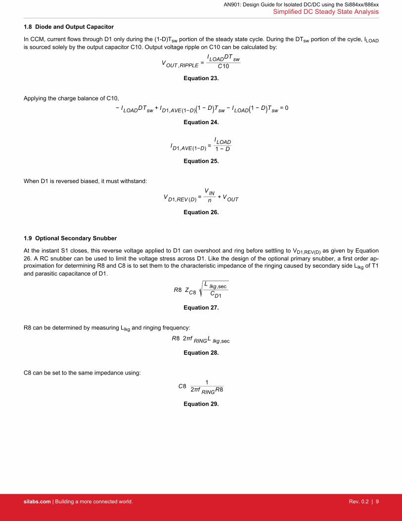
Figure 2.3 Simplified Bode Magnitude Plot of the Loop in PI Mode on page 16shows the magnitude Bode plot of the loop in PI mode.
AN901: Design Guide for Isolated DC/DC using the Si884xx/886xxDynamic Response
silabs.com | Building a more connected world. Rev. 0.2 | 15
1
10
100
1000
10000
100000
1000000
1 10 100 1000 10000 100000 1000000
Frequency (rad/s)
ADC,PI
ADC,P
0dBGai
n (d
B)
RO,gmfbC11 R7 x C11 RLOADC10
Figure 2.3. Simplified Bode Magnitude Plot of the Loop in PI Mode
AN901: Design Guide for Isolated DC/DC using the Si884xx/886xxDynamic Response
silabs.com | Building a more connected world. Rev. 0.2 | 16

3. Design Example
Consider the desired requirements listed in Table 3.1 Design Requirements on page 17.
Table 3.1. Design Requirements
Parameter Value
Input Voltage 24.0 V
Output Voltage 5.0 V
Input Voltage Ripple ≤ 50 mV
Output Voltage Ripple ≤ 50 mV
Maximum Output Current 1 A
AN901: Design Guide for Isolated DC/DC using the Si884xx/886xxDesign Example
silabs.com | Building a more connected world. Rev. 0.2 | 17

3.1 Transformer Design
For this example, operating in CCM was chosen. Equation 7. establishes the relationship between turns ratio n and duty cycle D. Ac-counting for forward voltage drop across D1 of 0.5 V and targeting a duty cycle of 40%, Equation 7. can be solved for transformer turnsratio n:
n �V IN ,D
(VOUT + Vf D1)(1 − D) � 24 * 0.45.5 * 0.6 �2.91
Equation 45.
A 3:1 turns ratio was chosen.
The next parameters to choose are the switching period and primary inductance. The Si886xx has externally set switching frequencyrange of 200 kHz to 900 kHz. 500 kHz was chosen for this example. C6 is set to 470 nF and R13 is calculated by rearranging Equation31:
R13 =1025.5 *Tsw
C6 = 1025.5 * 2x10−6
470x10−9 = 4.36kΩ
Equation 46.
R13 was set to 4.32 kΩ as that is the closest 1% resistor value.
To determine Lm, consider at what minimum load should the converter operate in CCM. For this design, it was targeted to operate inCCM between 70% and full load. At the cross-over point between DCM and CCM:
ImAVE ,XOVR =ImRIPPLE
2
Equation 47.
Substituting,0.7 * ILOADn(1 − D) =
V INDTsw2L m
Equation 48.
And solving for Lm:
L m =nV IND(1 − D)Tsw
1.4 * ILOAD= 3 * 24 * 0.4 * 0.6 * 2x10−6
1.4 = 24.7uH
Equation 49.
A transformer with turns ratio of 3:1 and primary inductance of 25 µH was chosen.
AN901: Design Guide for Isolated DC/DC using the Si884xx/886xxDesign Example
silabs.com | Building a more connected world. Rev. 0.2 | 18

3.2 R12 Sense Resistor Selection
R12 is chosen to provide a cycle by cycle current limit. Equation 11. gives the average magnetizing current at specified load.
Magnetizing Current
ImAVE =ILOADn(1 − D) = 1
3 * 0.6 = 556mA
Equation 50.
The peak current in CCM is:
Im,PK ,RCM = Im,AVE +V INDTsw
2L m= 0.556 + 24 * 0.4 * 2x10−6
2 * 25x10−6 = 0.94A
Equation 51.
Allowing for some variation in performance from design calculations, 1 A current limit is chosen. Applying Equation 14. and calculatingfor R12:
R12 = 100mVIm,LIMIT
= 0.11 = 100 mΩ
Equation 52.
Figure 3.1 Magnetizing Current on page 19 shows the expected magnetizing current waveform at specified load.
Peak Current Limit
DTsw
Im,RIPPLE
Im,AVE
(1-D)Tsw
Time (μS)
Cur
rent
(A)
Figure 3.1. Magnetizing Current
AN901: Design Guide for Isolated DC/DC using the Si884xx/886xxDesign Example
silabs.com | Building a more connected world. Rev. 0.2 | 19

3.3 Q1 Selection
The instant S1 opens, Q1’s drain voltage increases rapidly from nearly 0 V and settles to:Vds1,(1−D) = V IN + n(VOUT + V fD1) = 24 + 16.5 = 40.5V
Equation 53.
However, energy stored in Llkg must be dissipated in the secondary which causes Vds,(D) to spike a higher voltage. Q1 must be able totolerate this voltage spike between drain and source.
A N-channel MOSFET with 100 V rating was chosen to accommodate the expected voltage stress caused by Llkg
3.4 D1 Selection
Equation 25. and Equation 26. define the requirements for D1. Substituting into Equation 25.,
ID1′AVE (1−D) =ILOAD1 − D = 1
0.6 = 1.6A
Equation 54.
Diode current capacities are specified in rms. Assuming a linear current through D1, consider the translation of average to rms:
ID1′RMS (1−D) = ID1,AVE (1−D)( 23 ) = 1.84A
Equation 55.
Substituting into Equation 26.:
VD1,REV (D) =V INn + VOUT = 24
3 + 5 = 13V
Equation 56.
Equation 25. and Equation 26. do not include the voltage spike due to the interaction of the diode capacitance and secondary sideleakage inductance, and as a result, a diode with a larger withstanding voltage is required in practice.
When selecting D1, diodes with low Vf are the preferred choice as it minimizes the associated power loss.
PD1(1−D) = Vf D1 * ID1,AVE (1−D)
Equation 57.
Several diodes were tested in the circuit. A 5 A, 50 V diode was chosen for its tolerance to high operating temperatures at which diodeleakage and package heat transfer characteristics affect overall performance and efficiency.
3.5 External Regulator Circuit
For this design, an external regulator circuit was designed to work with the VREGA voltage reference to create a regulated supply forVDDA. R14 was selected for a 950 µA sink current.
R14 =V IN − VREGA
IR= 24 − 4.85
0.001 = 19.5kΩ
Equation 59.
R14 was set to 19.6 kΩ and C14 to the recommended 0.1 μF. MMBT2222 was selected for Q1.
AN901: Design Guide for Isolated DC/DC using the Si884xx/886xxDesign Example
silabs.com | Building a more connected world. Rev. 0.2 | 20

3.6 C10 Selection
C10 is inversely proportional to output voltage ripple and sets the crossover frequency of control loop gain. Solving Equation 21.,
C10 =ILOADDT swVOUT ,RIPPLE
≥ 1 * 0.4 * 2x10−6
0.05 ≥ 16uF
Equation 59.
Capacitor current in rms is given by:
IrmsC10 = ILOADD
1 − D = 1 * 0.40.6 = 0.81A
Equation 60.
A 22 μF X7R capacitor in 1210 package was chosen.
3.7 C2 Selection
In most applications, VIN also supplies the VDDA pin that powers the dc-dc controller and left side digital isolator circuitry. It is recom-mended to minimize voltage ripple at VDDA. Solving Equation 20.:
C2 ≥ILOADDTsw
V IN ,RIPPLE * n ≥ 1 * 0.4 * 2x10−6
0.05 * 3 ≥ 5.33μF
Equation 61.
A 10 μF X7R capacitor in 1210 package was chosen.
3.8 R5 and R6 Selection
The ratios of R5 and R6 are determined by the 5 V output voltage requirement. To reduce the dependence of feedback gain on theinternal error amplifier transconductance, it is recommended to have the parallel combination resistance to be ≥10 kΩ. Higher values ofR5 and R6 reduce power loss through the divider, but at the expense of increasing output voltage error due to IVSNS, which varies partto part. So R5 and R6 are chosen to target 10 kΩ parallel resistance.
10x103 = R5 *R6R5 + R6
Equation 62.
5 = 1.05( R5R6 + 1)
Equation 63.
Substituting Equation 51. into Equation 52. and solving for R6,
10x103 = 3.76R64.76 , R6 = 12.66x10³, R5 = 48.1x10³
Equation 64.
The nearest 1% resistor to 12.66 kΩ is 12.7 kΩ. However, setting R5 to either 47.5 kΩ or 48.7 kΩ does not target exactly 5 V as well asother 1% resistor pairs. A better match was found with R6 = 13.3 kΩ and R5 = 49.9 kΩ.
AN901: Design Guide for Isolated DC/DC using the Si884xx/886xxDesign Example
silabs.com | Building a more connected world. Rev. 0.2 | 21

3.9 Compensation Network
The compensation network is comprised of R7 and C11. R7 is selected to match RINT and 100 kΩ is the nearest 1% resistor value. TheC11 places the compensation zero in relationship to the crossover frequency. The equation for crossover frequency can be obtained bymultiplying the P-mode gain (Equation 33.), by the frequency of the pole created by RLOAD and C10 (Equation 38.):
f c �100x103 * 3nRLOAD
R5 * 12πRLOADC10 �12.1kHz
Equation 65.
To achieve good phase margin, it suggested to place the compensation zero near the pole created by RLOAD and C10.
C11 = 62π f c *R7 = 6
2π * 12.1x103 * 49.9x103 = 1.58nF
Equation 66.
A 1.5 nF capacitor was chosen.
AN901: Design Guide for Isolated DC/DC using the Si884xx/886xxDesign Example
silabs.com | Building a more connected world. Rev. 0.2 | 22

3.10 Primary Snubber
Without R19 and C16 installed, Vds of Q1 was measured to spike at 108 V and ring briefly at 30 MHz until the energy stored in Llkgdissipated. See Figure 3.2 Undamped Vds Ringing on page 23:
Q1 VDS,MAX = 100V
V: 20V/divH: 50ns/div
Figure 3.2. Undamped Vds Ringing
T1 was removed from the board and its primary inductance leakage was measured to be 456 nH. Applying Equation 17 and Equation18., R16 and C19 were calculated:
R16 = 2π f ringL lkg = 2π * 30x106 * 456x10−9 = 86Ω
Equation 67.
C19 = 12π f ringR16 = 1
2π * 30x106 * 86= 62pF
Equation 68.
Closest standard component values of R16 = 82 Ω and C19 = 68 pF were selected and installed. Q1 Vds was measured again to gageeffectiveness of the RC snubber. Voltage spike was reduced to 74 V as shown in Figure 3.3 Damped Vds Ringing on page 24.
AN901: Design Guide for Isolated DC/DC using the Si884xx/886xxDesign Example
silabs.com | Building a more connected world. Rev. 0.2 | 23

Figure 3.3. Damped Vds Ringing
R8 and C8 on the secondary side can be selected using the same methodology. Without a secondary side snubber, the voltage spikeacross D1 at the instant that S1 closes was measured to be 35 V with a ringing frequency of 59 MHz. T1 was removed from the boardand its primary inductance leakage was measured to be 74 nH.
R8 = 2π f ringL lkg = 2π * 59x106 * 74x10−9 = 27.4Ω
Equation 69.
C8 = 12π f ringR8 = 1
2π * 59x106 * 27.4= 98.4pF
Equation 70.
R8 is a 1% resistor value and C8 of 100 pF was chosen. The voltage spike was reduced to 23 V and the ringing damped.
AN901: Design Guide for Isolated DC/DC using the Si884xx/886xxDesign Example
silabs.com | Building a more connected world. Rev. 0.2 | 24

3.11 Design Summary
The table below shows the component selection that meets design requirements.
Table 3.2. Ordering Guide
Part Reference Description Manufacturer Manufacturer Part Number
C2 CAP, 10 μF, 50 V, ±20%, X7R, 1210 Venkel C1210X7R500-106M
C6 CAP, 0.4 μF, 16 V, ±10%, X7R, 0805 Venkel C0805X7R160-474K
C8 CAP, 100 pF, 50 V, ±10%, X7R, 0603 Venkel C0603X7R500-101K
C10 CAP, 22 μF, 25 V, ±10%, X7R, 1210 Venkel C1210X7R250-226M
C11 CAP, 1.5 nF, 25 V, ±10%, X5R, 0603 Venkel C0603X5R250-152K
C14 CAP, 0.1 μF, 10 V, ±10%, X7R, 0603 Venkel C0603X7R100-104K
C19 CAP, 68 pF, 100 V, ±10%, C0G, 0603 Venkel C0603C0G101-680K
D1 DIO, SUPER BARRIER, 50 V, 5.0 A, SMA Diodes Inc. SBRT5A50SA
Q1 TRANSISTOR, MOSFET, N-CHNL, 100 V, 3.7 A, 3 W,Switching, SOT223
Fairchild FDT3612
Q2 TRANSISTOR, NPN, 30V, 600mA, SOT23 On Semi MMBT2222LT1
R5 RES, 49.9 K, 1/16 W, ±1%, ThickFilm, 0603 Venkel CR0603-16W-4992F
R6 RES, 13.3 K, 1/16 W, ±1%, ThickFilm, 0603 Venkel CR0603-16W-1332F
R7 RES, 100 K, 1/10 W, ±1%, ThickFilm, 0603 Venkel CR0603-10W-1003F
R8 RES, 27.4 Ω, 1/10 W, ±1%, ThickFilm, 0603 Venkel CR0603-10W-27R4F
R12 RES, 0.1 Ω, 1/2 W, ±1%, ThickFilm, 1206 Venkel LCR1206-R100F
R13 RES, 4.32 K, 1/10 W, ±1%, ThickFilm, 0603 Venkel CR0603-10W-4321F
R14 RES, 19.6 K, 1/16 W, ±1%, ThickFilm, 0603 Venkel CR0603-16W-1962F
R16 RES, 82.0 Ω, 1/10 W, ±1%, ThickFilm, 0603 Venkel CR0603-10W-82R0F
T1 TRANSFORMER, Flyback, 25 μH Primary, 500 nH Leak-age, 3:1, SMT
UMEC UTB02205s
U1 IC, ISOLATOR, DC DC External Switch,Freq Control, 2 Digital Ch, SO20 WB
Silicon Labs Si88621ED-IS
AN901: Design Guide for Isolated DC/DC using the Si884xx/886xxDesign Example
silabs.com | Building a more connected world. Rev. 0.2 | 25

http://www.silabs.com
Silicon Laboratories Inc.400 West Cesar ChavezAustin, TX 78701USA
Simplicity StudioOne-click access to MCU and wireless tools, documentation, software, source code libraries & more. Available for Windows, Mac and Linux!
IoT Portfoliowww.silabs.com/IoT
SW/HWwww.silabs.com/simplicity
Qualitywww.silabs.com/quality
Support and Communitycommunity.silabs.com
DisclaimerSilicon Labs intends to provide customers with the latest, accurate, and in-depth documentation of all peripherals and modules available for system and software implementers using or intending to use the Silicon Labs products. Characterization data, available modules and peripherals, memory sizes and memory addresses refer to each specific device, and "Typical" parameters provided can and do vary in different applications. Application examples described herein are for illustrative purposes only. Silicon Labs reserves the right to make changes without further notice and limitation to product information, specifications, and descriptions herein, and does not give warranties as to the accuracy or completeness of the included information. Silicon Labs shall have no liability for the consequences of use of the information supplied herein. This document does not imply or express copyright licenses granted hereunder to design or fabricate any integrated circuits. The products are not designed or authorized to be used within any Life Support System without the specific written consent of Silicon Labs. A "Life Support System" is any product or system intended to support or sustain life and/or health, which, if it fails, can be reasonably expected to result in significant personal injury or death. Silicon Labs products are not designed or authorized for military applications. Silicon Labs products shall under no circumstances be used in weapons of mass destruction including (but not limited to) nuclear, biological or chemical weapons, or missiles capable of delivering such weapons.
Trademark InformationSilicon Laboratories Inc.® , Silicon Laboratories®, Silicon Labs®, SiLabs® and the Silicon Labs logo®, Bluegiga®, Bluegiga Logo®, Clockbuilder®, CMEMS®, DSPLL®, EFM®, EFM32®, EFR, Ember®, Energy Micro, Energy Micro logo and combinations thereof, "the world’s most energy friendly microcontrollers", Ember®, EZLink®, EZRadio®, EZRadioPRO®, Gecko®, ISOmodem®, Precision32®, ProSLIC®, Simplicity Studio®, SiPHY®, Telegesis, the Telegesis Logo®, USBXpress® and others are trademarks or registered trademarks of Silicon Labs. ARM, CORTEX, Cortex-M3 and THUMB are trademarks or registered trademarks of ARM Holdings. Keil is a registered trademark of ARM Limited. All other products or brand names mentioned herein are trademarks of their respective holders.