Embed Size (px)
DESCRIPTION
Â
Citation preview
SA50-28-5/15T Rev A Microsemi Corp. Page 1 of 14
Power Management Group
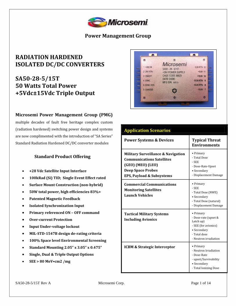
RADIATION HARDENED ISOLATED DC/DC CONVERTERS
SA50-28-5/15T 50 Watts Total Power +5Vdc±15Vdc Triple Output
Microsemi Power Management Group (PMG)
multiple decades of fault free heritage complex custom
(radiation hardened) switching power design and systems
are now complimented with the introduction of “SA Series”
Standard Radiation Hardened DC/DC converter modules
Standard Product Offering
+28 Vdc Satellite Input Interface
100kRad (Si) TID; Single Event Effect rated
Surface Mount Construction (non-hybrid)
50W total power, high efficiencies 83%+
Patented Magnetic Feedback
Isolated Synchronization Input
Primary referenced ON – OFF command
Over-current Protection
Input Under-voltage lockout
MIL-STD-1547B design de-rating criteria
100% Space level Environmental Screening
Standard Mounting 2.05” x 3.05” x 0.475”
Single, Dual & Triple Output Options
SEE > 80 MeV•cm2 /mg
Application Scenarios
Power Systems & Devices Typical Threat Environments
Military Surveillance & Navigation
Communications Satellites
(GEO) (MEO) (LEO)
Deep Space Probes
EPS, Payload & Subsystems
• Primary
- Total Dose
- SEE
- Dose-Rate-Upset
• Secondary
- Displacement Damage
Commercial Communications
Monitoring Satellites
Launch Vehicles
• Primary
- SEE
- Total Dose (NWE)
• Secondary
- Total Dose (natural)
- Displacement Damage
Tactical Military Systems
Including Avionics
• Primary
- Dose-rate (upset & Latch up)
- SEE (for avionics)
• Secondary
- Total dose
- Neutron irradiation
ICBM & Strategic Interceptor • Primary
- Neutron Irradiation
- Dose-Rate
- upset/Survivability
• Secondary
- Total Ionizing Dose
SA50-28-5/15T Rev A Microsemi Corp. Page 2 of 14
Radiation Performance Rating
All bipolar microcircuits contained within the SA50 series
design are characterized for enhanced low dose rate
sensitivity (ELDRS), with data constructed at a dose rate
of 0.01 rad (Si)/s or less with assessments in both a
biased and unbiased state
Qualification and Acceptance Testing
Qualification and inspection/testing minimally include;
Random Vibration, Mechanical Shock, Thermal Vacuum,
Thermal Cycling, EMI, and Burn-in testing with periodic
corresponding performance measurements as required.
All converter modules are pre-screened according to
specific in-line acceptance testing. These processes
include multiple cycles of High and Low temperature
cycling, Random vibration, with Pre and Post Electrical
Performance Verification prior to delivery.
Parts, Materials and Processes
Internal electronic components are selected and
screened in accordance with GSFC EEE-INST-002
(Instruction for EEE Parts Selection, Screening, and
Qualification).
Magnetics are designed, manufactured and screened in
accordance with MIL-STD-981. Group B and
Qualification test per MIL-STD-981 can be performed if
required by the customer at additional charge. Part De-
rating is in accordance with MIL-STD-1547B and MIL-
STD-975M. The enclosure is of machined Aluminum
construction. The finish is conductive Alodyne per MIL-
C-5541, Type 3.
Note: The product may be upgraded to meet TOR-
2006(8583)-5236 requirements at the customer’s
request.
Workmanship is in accordance with the highest industry
standards, including ANSI/STD-001 Class 3.
Alternate Version (-P)
The SA50 series alternate version is offered for
prototypes and less stringent flight applications.
Selective component alternatives are employed within
the design, specifically by utilizing “B” level or lower
component substitutions. The part substitutions do not
impact electrical performance characteristics.
Test Min Typ Unit
Total Ionizing Dose
(Gamma) 100 300 kRads (Si)
Single Event Effects
SEU, SEL, SEGR, SEB
LET 82
(129Xe) MeV•cm2 /mg
SA50-28-5/15T Rev A Microsemi Corp. Page 3 of 14
Ratings
Electrical Specifications
Absolute Maximum Ratings Recommended Operating Conditions
VIN range -0.5Vdc to +60Vdc VIN range +17Vdc to +50Vdc
Output power 50 Watts
Lead temperature +300°C for 10 Sec.
Operating temperature -55°C to +125°C
Storage temperature -55°C to +125°C Output power 2 watts to Max. Rated
Shock
1500 gpk, 0.5 msec
½ sineOperating temperature c -55°C to +125°C
Constant Acceleration 50 g Operating temperature a,b -55°C to +70°C
Random Vibration 24.06 grms , 50-2000 Hz
a
b
c
Meets derating per MIL-STD-975M
Meets derating per MIL-STD-1547B
For operation at +125°C see table Note 15
Min Nom Max
Input Voltage 1,2,3 Note 2 17 28 50 V
(main) 5.08 5.10 5.12
(aux.) 14.46 14.75 15.05
(main) 5.05 5.10 5.15
(aux.) 14.25 14.75 15.25
Output Power (POUT) 1,2,3 VIN = 17, 28, 50 Volts, Notes 2,4 5 50 W
(main) 400 4000
(aux.) 100 1000
(main) -10 10
(aux.) -150 150
(main) -50 50
(aux.) -500 500
(aux.) 1,2,3
VIN = 17, 28, 50 Volts
IOUT = 2.5A to 1A and 2.5A to 4A on main
and ±half rated on aux. outputs
-3.00 3.00 %
Output Voltage ( VOUT )
1 IOUT = 100% rated load, Note 5 V
2,3 IOUT = 100% rated load, Note 5 V
Parameter
Group A
Subgroup
1 25°C
2 -55°C
3 85°C
Conditions
-55°C ≤ TCASE ≤ +85°C
VIN = 28V DC ± 5%, CL = 0
unless otherwise specified
Limits Unit
Load regulation ( VRLOAD)
1,2,3 VIN = 17, 28, 50 Volts
IOUT =10%, 50%, 100% rated, Note 5, 13 mV
Output current (IOUT)
1,2,3 VIN = 17, 28, 50 Volts, Notes 2,3,4,5 mA
Line regulation ( VRLINE )
1,2,3 VIN = 17, 28, 50 Volts
IOUT =10%, 50%, 100% rated, Notes 5, 14 mV
Cross regulation (VRCROSS)
SA50-28-5/15T Rev A Microsemi Corp. Page 4 of 14
Min Nom Max
IOUT = 0, Pin 3 open 100 150
Pin 3 shorted to pin 2 2.0 5.0
(main) 25 50
(aux.) 37.5 75
Switching frequency (FS) 1,2,3 Sync. Input (Pin 4) open 200 220 240 kHz
Efficiency ( EFF ) 1,2,3 IOUT = 100% rated load, Note 5 80 83 %
ON voltage (or Open Collector) 4.5 V
OFF drive current (sink) 1000 μA
OFF voltage 2 V
frequency range 250 300 kHz
pulse high level 4.0 10.0 V
pulse low level -0.5 0.5 V
pulse transition rate 200 V/μs
pulse duty cycle 10 80 %
Current Limit Point
Expressed as a % of full rated
output current
1,2,3 VOUT = 90% of Nominal, Note 5 105 135 %
Overshoot (VOS) (main) 500 mV
Overshoot (VOS) (aux.) 750 mV
Turn-on Delay (TDLY) 1.0 5.0 mSec
(main) 1000 μF
(Each aux. output) 200 μF
MTBF MIL-HDBK-217F2, SF, 35°C 8.22E+06 Hrs
1,2,3 VIN = 17, 28, 50 Volts
IOUT = 100% rated load, Notes 5, 6 mV p-p
Inhibit Input
Note 1
Input current (IIN) 1,2,3 mA
Output ripple (VRIP)
Group A
Subgroup
1 25°C
2 -55°C
3 85°C
Conditions
-55°C ≤ TCASE ≤ +85°C
VIN = 28V DC ± 5%, CL = 0
unless otherwise specified
Limits Unit
W
Output response to
step load changes (VTLD) 4,5,6
Half Load to/from Full Load, Notes 5,9-300 300 mV pk
Synchronization Input
Ext. Clock on Sync. Input (Pin 4)
Note 1
Power dissipation,
load fault (PD) 1,2,3 Short Circuit, Overload, Note 8 18
μSec
Output response
to step line changes (VTLN)
17V to/from 50V
IOUT = 100% rated load, Notes 1, 5,11 -300 300 mV pk
Recovery time,
step load changes (TTLD) 4,5,6
Half Load to/from Full Load, Note 5,9,10 50 200
μs
Turn-on Response
4,5,6 No Load, Full Load
Notes 5,12
Recovery time,
step line changes (TTLN)
17V to/from 50V
IOUT = 100% rated load, Notes 1, 5,11 50 200
Capacitive Load (CL)
IOUT = 100% rated load, No effect on DC
performance, Notes 1, 5, 7
Line Rejection DC to 50KHz, Notes 1, 5
IOUT = 100% rated load 40 60 dB
Isolation 1
Input (Pins 1,2,3) to Outputs
Any Pin to Case (except pin 6)
Sync and Sync Rtn to any pin and case
100 MΩ
gDevice Weight 110
SA50-28-5/15T Rev A Microsemi Corp. Page 5 of 14
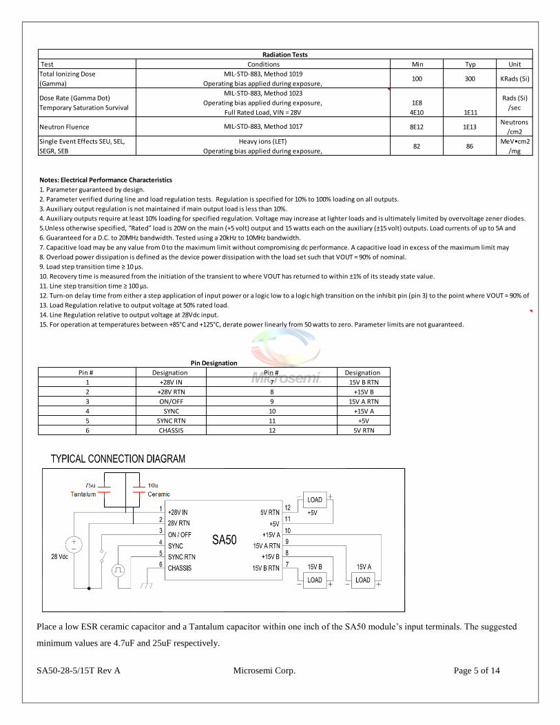
Place a low ESR ceramic capacitor and a Tantalum capacitor within one inch of the SA50 module’s input terminals. The suggested
minimum values are 4.7uF and 25uF respectively.
Test Min Typ Unit
Total Ionizing Dose
(Gamma) 100 300 KRads (Si)
Dose Rate (Gamma Dot)
Temporary Saturation Survival 1E8
4E10
1E11
Rads (Si)
/sec
Neutron Fluence 8E12 1E13 Neutrons
/cm2
Single Event Effects SEU, SEL,
SEGR, SEB 82 86
MeV•cm2
/mg
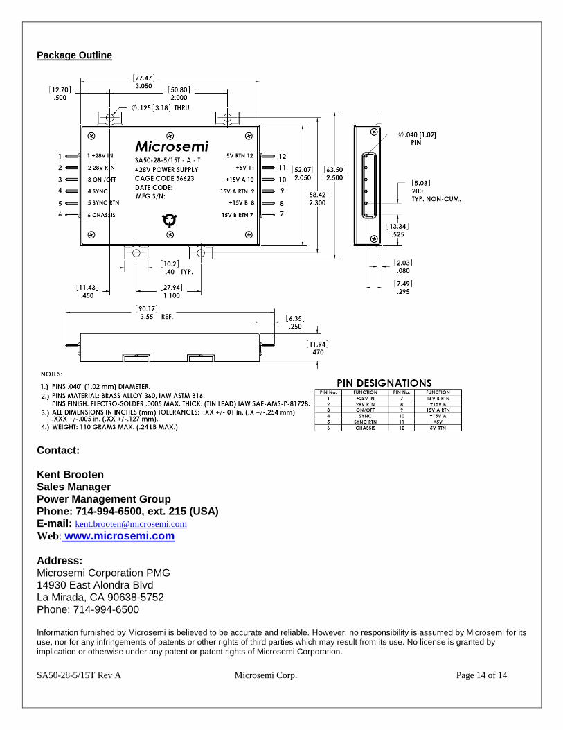
Pin # Designation Pin # Designation
1 +28V IN 7 15V B RTN
2 +28V RTN 8 +15V B
3 ON/OFF 9 15V A RTN
4 SYNC 10 +15V A
5 SYNC RTN 11 +5V
6 CHASSIS 12 5V RTN
Heavy ions (LET)
Operating bias applied during exposure,
Notes: Electrical Performance Characteristics
1. Parameter guaranteed by design.
2. Parameter verified during line and load regulation tests. Regulation is specified for 10% to 100% loading on all outputs.
3. Auxiliary output regulation is not maintained if main output load is less than 10%.
4. Auxiliary outputs require at least 10% loading for specified regulation. Voltage may increase at lighter loads and is ultimately limited by overvoltage zener diodes.
Radiation Tests
Conditions
MIL-STD-883, Method 1019
Operating bias applied during exposure,
MIL-STD-883, Method 1023
Operating bias applied during exposure,
Full Rated Load, VIN = 28V
MIL-STD-883, Method 1017
11. Line step transition time ≥ 100 μs.
12. Turn-on delay time from either a step application of input power or a logic low to a logic high transition on the inhibit pin (pin 3) to the point where VOUT = 90% of
13. Load Regulation relative to output voltage at 50% rated load.
14. Line Regulation relative to output voltage at 28Vdc input.
15. For operation at temperatures between +85°C and +125°C, derate power linearly from 50 watts to zero. Parameter limits are not guaranteed.
Pin Designation
5.Unless otherwise specified, “Rated” load is 20W on the main (+5 volt) output and 15 watts each on the auxiliary (±15 volt) outputs. Load currents of up to 5A and
6. Guaranteed for a D.C. to 20MHz bandwidth. Tested using a 20kHz to 10MHz bandwidth.
7. Capacitive load may be any value from 0 to the maximum limit without compromising dc performance. A capacitive load in excess of the maximum limit may
8. Overload power dissipation is defined as the device power dissipation with the load set such that VOUT = 90% of nominal.
9. Load step transition time ≥ 10 μs.
10. Recovery time is measured from the initiation of the transient to where VOUT has returned to within ±1% of its steady state value.
SA50-28-5/15T Rev A Microsemi Corp. Page 6 of 14
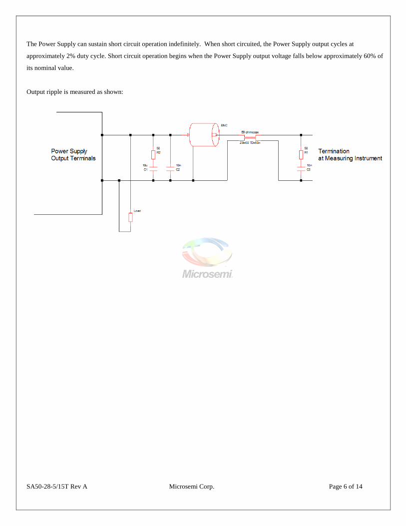
The Power Supply can sustain short circuit operation indefinitely. When short circuited, the Power Supply output cycles at
approximately 2% duty cycle. Short circuit operation begins when the Power Supply output voltage falls below approximately 60% of
its nominal value.
Output ripple is measured as shown:
SA50-28-5/15T Rev A Microsemi Corp. Page 7 of 14
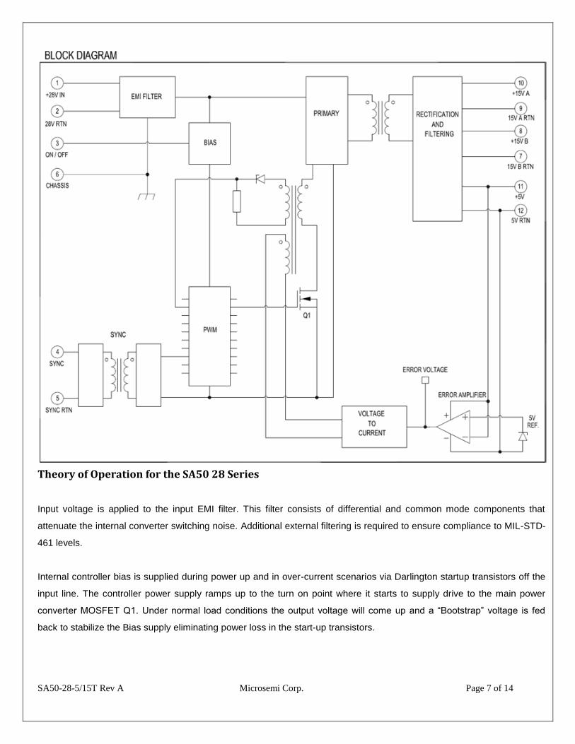
Theory of Operation for the SA50 28 Series
Input voltage is applied to the input EMI filter. This filter consists of differential and common mode components that
attenuate the internal converter switching noise. Additional external filtering is required to ensure compliance to MIL-STD-
461 levels.
Internal controller bias is supplied during power up and in over-current scenarios via Darlington startup transistors off the
input line. The controller power supply ramps up to the turn on point where it starts to supply drive to the main power
converter MOSFET Q1. Under normal load conditions the output voltage will come up and a “Bootstrap” voltage is fed
back to stabilize the Bias supply eliminating power loss in the start-up transistors.

SA50-28-5/15T Rev A Microsemi Corp. Page 8 of 14
Main power conversion occurs in the forward converter Q1 and associated Transformer. The secondary windings develop
the required output voltages in parallel. A coupled inductor promotes good output cross regulation. Elimination of
secondary side post regulators promotes high efficiency performance.
Output voltages are regulated on the main output secondary side. A TL1431 reference develops a current mode error
signal which is chopped by the main forward transformer voltage and the summed with the primary side converter current
in a patented magnetic feedback approach. The combined “V + I” error signal is applied to the primary controller’s ramp
control input to complete the regulation loop.
The primary ON OFF command disables internal switch-mode action when pulled low.
The SYNC input is fully transformer isolated to allow operation from primary or secondary referenced sync drives.
SA50-28-5/15T Rev A Microsemi Corp. Page 9 of 14
APPLICATION DATA
Under voltage Operation:
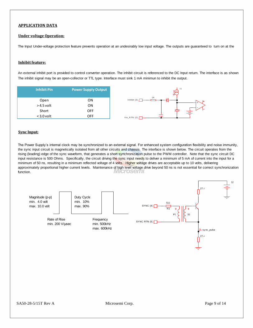
Inhibit feature:
Open ON
> 4.5 volt ON
Short OFF
< 3.0 volt OFF
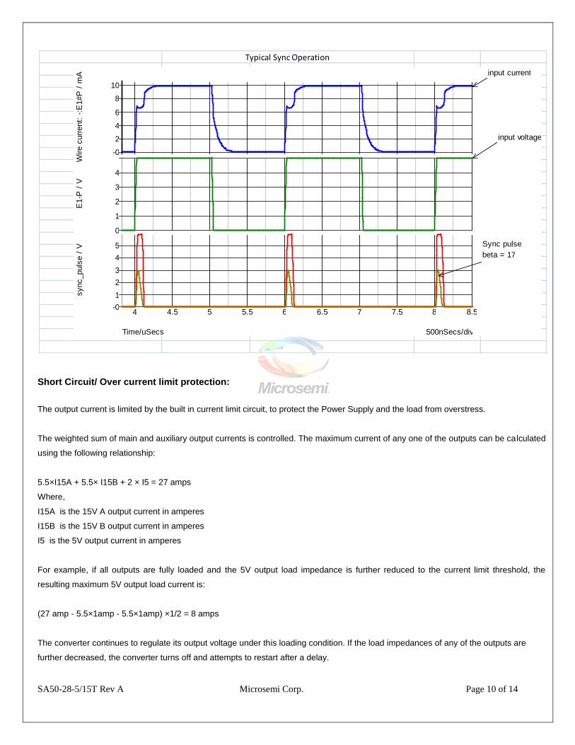
Sync Input:
The Power Supply’s internal clock may be synchronized to an external signal. For enhanced system configuration flexibility and noise immunity,
the sync input circuit is magnetically isolated from all other circuits and chassis. The interface is shown below. The circuit operates from the
rising (leading) edge of the sync waveform, that generates a short synchronization pulse to the PWM controller. Note that the sync circuit DC
input resistance is 500 Ohms. Specifically, the circuit driving the sync input needs to deliver a minimum of 5 mA of current into the input for a
minimum of 50 ns, resulting in a minimum reflected voltage of 4 volts. Higher voltage drives are acceptable up to 10 volts, delivering
approximately proportional higher current levels. Maintenance of high level voltage drive beyond 50 ns is not essential for correct synchronization
function.
The Input Under-voltage protection feature prevents operation at an undesirably low input voltage. The outputs are guaranteed to turn on at the
specified minimum input voltage and guaranteed to be disabled below 70% of the specified minimum input
An external inhibit port is provided to control converter operation. The inhibit circuit is referenced to the DC Input return. The interface is as shown
below. The inhibit signal may be an open-collector or TTL type. Interface must sink 1 mA minimun to inhibit the output.
Inhibit Pin Power Supply Output
V in _ R TN (2 )
1 K
I 1
I n h ib it (3 )
SYNC RTN (5)
SYNC (4)
12
27.4
27.4
P1 S1
sy nc_pulse
511
R1
Frequency
min. 500kHz
max. 600kHz
Rate of Rise
min. 200 V/µsec
Duty Cycle
min. 10%
max. 90%
Magnitude (p-p)
min. 4.0 volt
max. 10.0 volt
SA50-28-5/15T Rev A Microsemi Corp. Page 10 of 14
Short Circuit/ Over current limit protection:
The output current is limited by the built in current limit circuit, to protect the Power Supply and the load from overstress.
The weighted sum of main and auxiliary output currents is controlled. The maximum current of any one of the outputs can be calculated
using the following relationship:
5.5×I15A + 5.5× I15B + 2 × I5 = 27 amps
Where,
I15A is the 15V A output current in amperes
I15B is the 15V B output current in amperes
I5 is the 5V output current in amperes
For example, if all outputs are fully loaded and the 5V output load impedance is further reduced to the current limit threshold, the
resulting maximum 5V output load current is:
(27 amp - 5.5×1amp - 5.5×1amp) ×1/2 = 8 amps
The converter continues to regulate its output voltage under this loading condition. If the load impedances of any of the outputs are
further decreased, the converter turns off and attempts to restart after a delay.
Typical Sync Operation
Wire c
urr
ent:
-:E
1#P
/ m
A
-0
2
4
6
8
10E
1-P
/ V
0
1
2
3
4
Time/uSecs 500nSecs/div
4 4.5 5 5.5 6 6.5 7 7.5 8 8.5
sync_puls
e /
V
-0
1
2
3
4
5 Sync pulse
beta = 17
input voltage
input current
SA50-28-5/15T Rev A Microsemi Corp. Page 11 of 14
Model Numbering Scheme
PMG-28 Series Available Data Items: Analyses & Reports: 1: Mechanical Analysis 2: Stress Analysis 3: Thermal Analysis 4: Radiation Analysis 5: Worse Case Analysis 6: FEMA 7: First Article Qualification Test Report 8: EMI Test Report
Dual Output Configuration
The SA50-120 Triple configurations are readily configurable as Dual Output supplies.
For balanced output Dual Supply configuration, connect Pins 8 & 9 together to form the Dual Output Common potential. Pin 7 is now the
negative (–) Dual output and Pin 10 is the positive (+) Dual output. In this configuration it is important to preload the unused 5V output
with 12 ohms, representing a 10% of rated load on that output. This assures proper regulation and cross regulation of the dual outputs
over their full load ranges.
For an unbalanced Dual Supply configuration, connect the auxiliary outputs in parallel (Pin 10 to Pin 8 and Pin 9 to Pin 7). Since the
Auxiliary and Main outputs are internally isolated, it is allowable to connect either the main output as the high side dual supply
(Connect Pin 12 to Pin 10 for the Common output) or the Auxiliary output as the high side dual supply (Connect Pin 11 to Pin 9 for the
common output). Again please ensure that the main output load is at least 10% of rated.
Following the above guidelines, the regulation and cross regulation performance of the triple applies to the dual configurations in
general.
SA50-28-5/15T Rev A Microsemi Corp. Page 12 of 14
SA50 Mechanical Installation Application Note
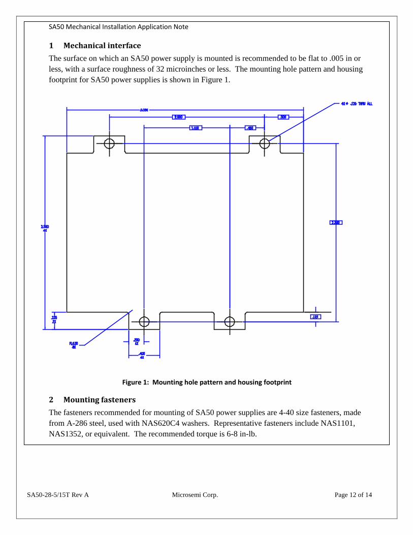
1 Mechanical interface
The surface on which an SA50 power supply is mounted is recommended to be flat to .005 in or
less, with a surface roughness of 32 microinches or less. The mounting hole pattern and housing
footprint for SA50 power supplies is shown in Figure 1.
Figure 1: Mounting hole pattern and housing footprint
2 Mounting fasteners
The fasteners recommended for mounting of SA50 power supplies are 4-40 size fasteners, made
from A-286 steel, used with NAS620C4 washers. Representative fasteners include NAS1101,
NAS1352, or equivalent. The recommended torque is 6-8 in-lb.
SA50-28-5/15T Rev A Microsemi Corp. Page 13 of 14
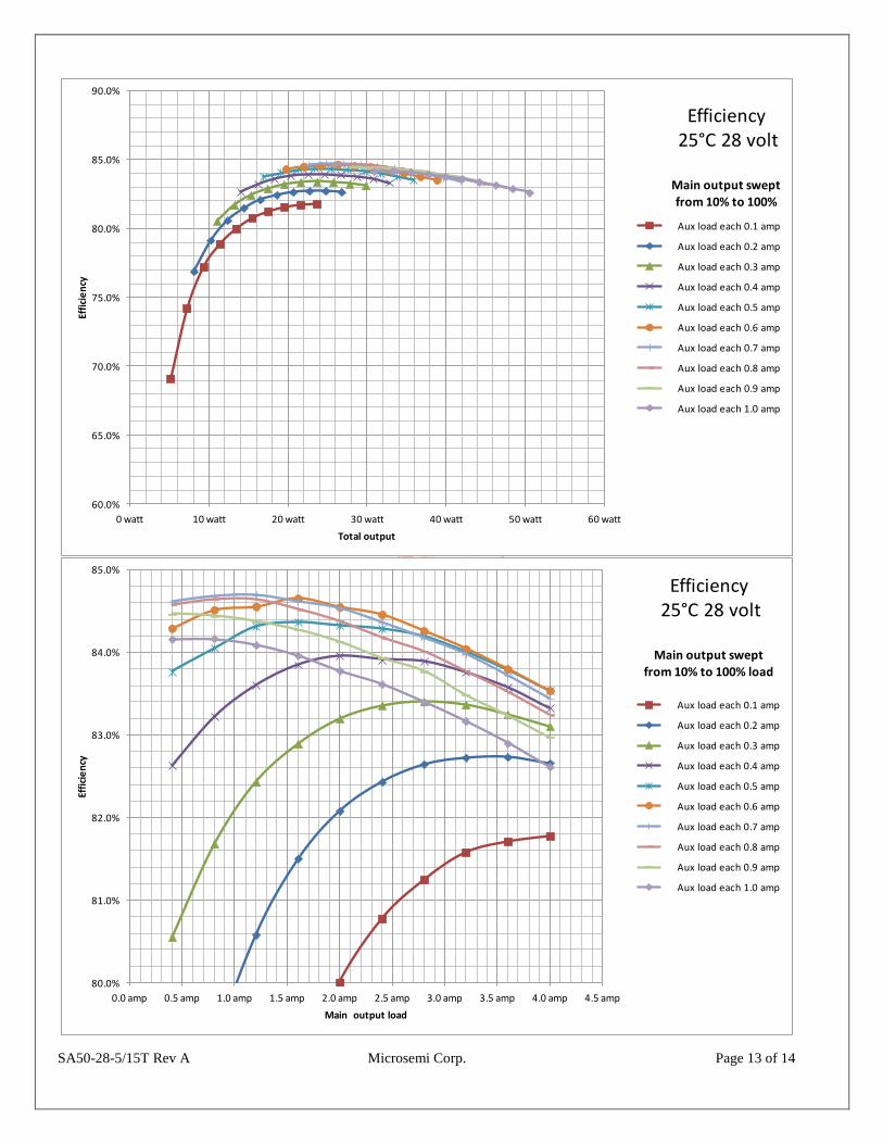
60.0%
65.0%
70.0%
75.0%
80.0%
85.0%
90.0%
0 watt 10 watt 20 watt 30 watt 40 watt 50 watt 60 watt
Effi
cie
ncy
Total output
Efficiency25°C 28 volt
Main output swept from 10% to 100%
Aux load each 0.1 amp
Aux load each 0.2 amp
Aux load each 0.3 amp
Aux load each 0.4 amp
Aux load each 0.5 amp
Aux load each 0.6 amp
Aux load each 0.7 amp
Aux load each 0.8 amp
Aux load each 0.9 amp
Aux load each 1.0 amp
80.0%
81.0%
82.0%
83.0%
84.0%
85.0%
0.0 amp 0.5 amp 1.0 amp 1.5 amp 2.0 amp 2.5 amp 3.0 amp 3.5 amp 4.0 amp 4.5 amp
Effi
cie
ncy
Main output load
Efficiency25°C 28 volt
Main output swept from 10% to 100% load
Aux load each 0.1 amp
Aux load each 0.2 amp
Aux load each 0.3 amp
Aux load each 0.4 amp
Aux load each 0.5 amp
Aux load each 0.6 amp
Aux load each 0.7 amp
Aux load each 0.8 amp
Aux load each 0.9 amp
Aux load each 1.0 amp
SA50-28-5/15T Rev A Microsemi Corp. Page 14 of 14
Package Outline
Contact: Kent Brooten Sales Manager Power Management Group Phone: 714-994-6500, ext. 215 (USA) E-mail: [email protected]
Web: www.microsemi.com
Address: Microsemi Corporation PMG 14930 East Alondra Blvd La Mirada, CA 90638-5752 Phone: 714-994-6500
Information furnished by Microsemi is believed to be accurate and reliable. However, no responsibility is assumed by Microsemi for its use, nor for any infringements of patents or other rights of third parties which may result from its use. No license is granted by implication or otherwise under any patent or patent rights of Microsemi Corporation.