Embed Size (px)
Citation preview
AN950: Si1153 User's Guide
This application note provides an outline for using the Si1153ambient-light and proximity sensors. General considerations ofelectrical and optical component selection, programming, andpower consumption are explained to cover the majority of situa-tions.Specific topics are discussed in other documents (see 7. Additional Resources) andmay help understanding. The physics of the Si114x series and the Si1153 have somedetails in common, and their respective data sheets may be consulted for more infor-mation.
KEY POINTS
• Discusses optical considerations towardmechanical design
• Explains electrical component selection• Shows proximity measurements• Includes programming guide• Provides information on latency• Explains power consumption calculations
silabs.com | Smart. Connected. Energy-friendly. Rev. 0.4
1. Optical Considerations toward Mechanical Design
This section focuses on mechanical and industrial design considerations.
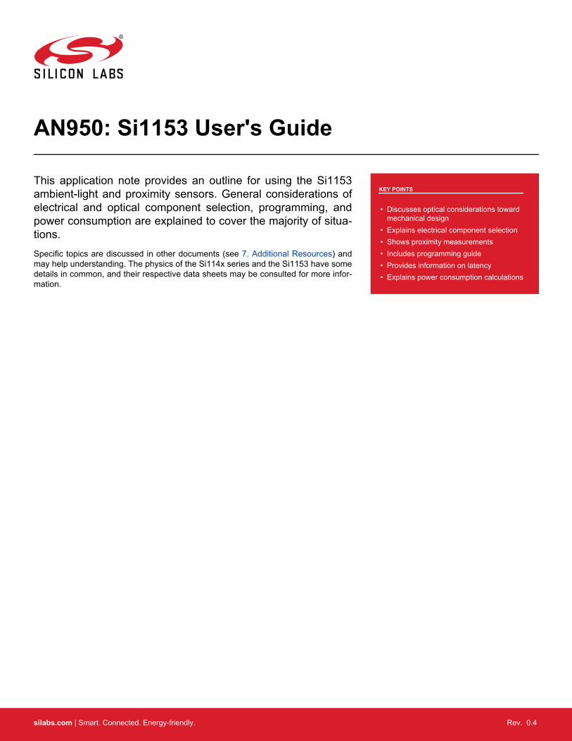
1.1 Topology
The following figure highlights and defines the various system topologies.
Figure 1.1. System Topologies
The purpose of the system topologies discussed is to provide a sense of the level of optical leakage or cross-talk expected in a proximi-ty system. One common misconception is that a system without an overlay and one with a transparent overlay are “the same”. Althoughthey might appear the same to the human eye, it is important to examine this from the perspective of the device.
AN950: Si1153 User's GuideOptical Considerations toward Mechanical Design
silabs.com | Smart. Connected. Energy-friendly. Rev. 0.4 | 1
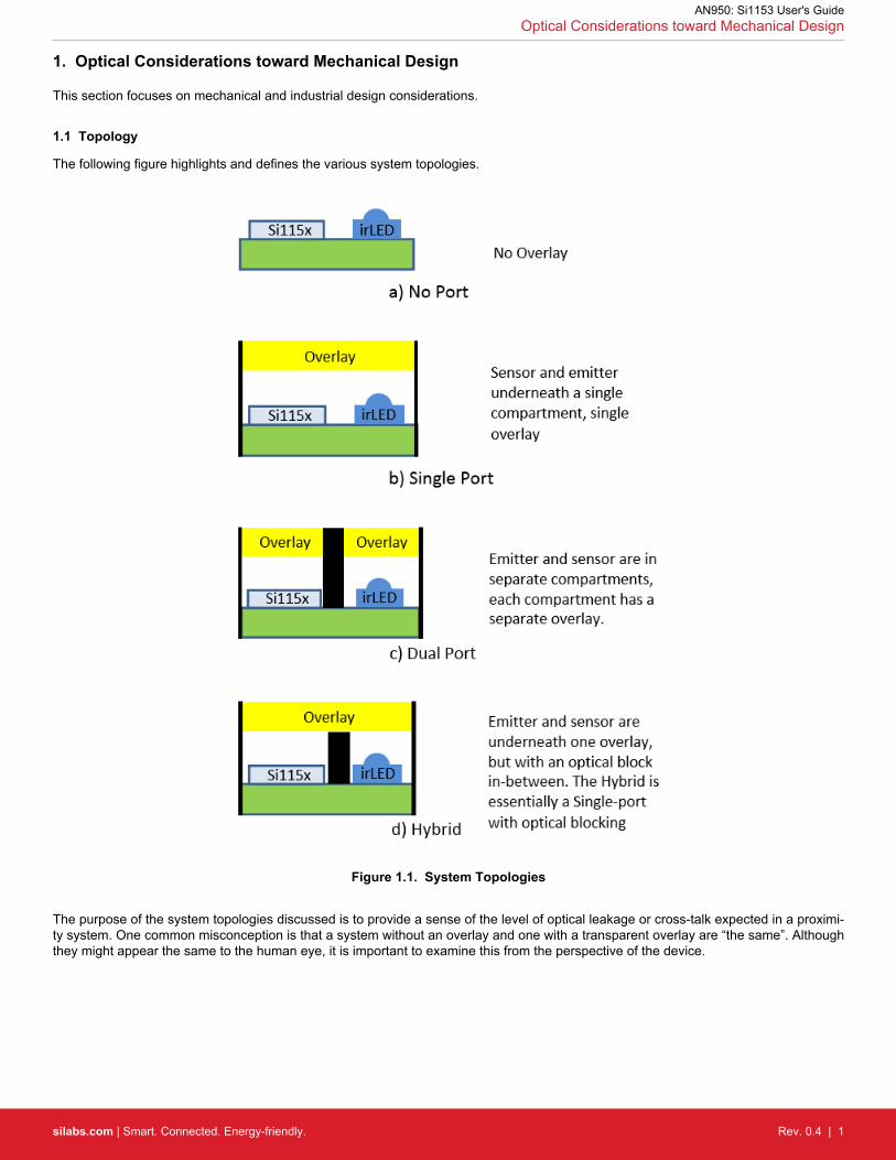
1.2 Optical Leakage
Also refer to 3. Proximity Measurements for information on how the Si115x makes Proximity Sense (PS) measurements.
Figure 1.2. Common Misconception
In a Single-Port system, there exists a reflection from the overlay. The magnitude of the reflection is a function of the index of refractionand the incident angle relative to the overlay surface normal. There is a set of equations called 'Fresnel's Equations' that provides aprediction as to the amount of light reflected back to the sensor.
In a No-Port system, the optical leakage from the overlay is not present. However, this does not mean that optical leakage does notexist. There may be optical paths causing the optical leakage other than the overlay.
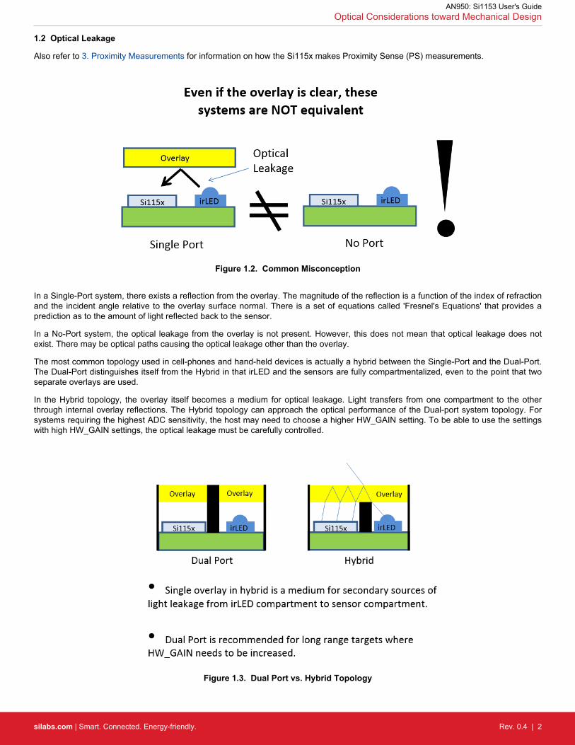
The most common topology used in cell-phones and hand-held devices is actually a hybrid between the Single-Port and the Dual-Port.The Dual-Port distinguishes itself from the Hybrid in that irLED and the sensors are fully compartmentalized, even to the point that twoseparate overlays are used.
In the Hybrid topology, the overlay itself becomes a medium for optical leakage. Light transfers from one compartment to the otherthrough internal overlay reflections. The Hybrid topology can approach the optical performance of the Dual-port system topology. Forsystems requiring the highest ADC sensitivity, the host may need to choose a higher HW_GAIN setting. To be able to use the settingswith high HW_GAIN settings, the optical leakage must be carefully controlled.
Figure 1.3. Dual Port vs. Hybrid Topology
AN950: Si1153 User's GuideOptical Considerations toward Mechanical Design
silabs.com | Smart. Connected. Energy-friendly. Rev. 0.4 | 2
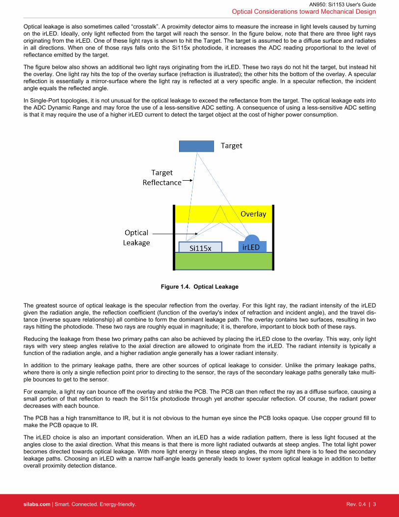
Optical leakage is also sometimes called “crosstalk”. A proximity detector aims to measure the increase in light levels caused by turningon the irLED. Ideally, only light reflected from the target will reach the sensor. In the figure below, note that there are three light raysoriginating from the irLED. One of these light rays is shown to hit the Target. The target is assumed to be a diffuse surface and radiatesin all directions. When one of those rays falls onto the Si115x photodiode, it increases the ADC reading proportional to the level ofreflectance emitted by the target.
The figure below also shows an additional two light rays originating from the irLED. These two rays do not hit the target, but instead hitthe overlay. One light ray hits the top of the overlay surface (refraction is illustrated); the other hits the bottom of the overlay. A specularreflection is essentially a mirror-surface where the light ray is reflected at a very specific angle. In a specular reflection, the incidentangle equals the reflected angle.
In Single-Port topologies, it is not unusual for the optical leakage to exceed the reflectance from the target. The optical leakage eats intothe ADC Dynamic Range and may force the use of a less-sensitive ADC setting. A consequence of using a less-sensitive ADC settingis that it may require the use of a higher irLED current to detect the target object at the cost of higher power consumption.
Figure 1.4. Optical Leakage
The greatest source of optical leakage is the specular reflection from the overlay. For this light ray, the radiant intensity of the irLEDgiven the radiation angle, the reflection coefficient (function of the overlay's index of refraction and incident angle), and the travel dis-tance (inverse square relationship) all combine to form the dominant leakage path. The overlay contains two surfaces, resulting in tworays hitting the photodiode. These two rays are roughly equal in magnitude; it is, therefore, important to block both of these rays.
Reducing the leakage from these two primary paths can also be achieved by placing the irLED close to the overlay. This way, only lightrays with very steep angles relative to the axial direction are allowed to originate from the irLED. The radiant intensity is typically afunction of the radiation angle, and a higher radiation angle generally has a lower radiant intensity.
In addition to the primary leakage paths, there are other sources of optical leakage to consider. Unlike the primary leakage paths,where there is only a single reflection point prior to directing to the sensor, the rays of the secondary leakage paths generally take multi-ple bounces to get to the sensor.
For example, a light ray can bounce off the overlay and strike the PCB. The PCB can then reflect the ray as a diffuse surface, causing asmall portion of that reflection to reach the Si115x photodiode through yet another specular reflection. Of course, the radiant powerdecreases with each bounce.
The PCB has a high transmittance to IR, but it is not obvious to the human eye since the PCB looks opaque. Use copper ground fill tomake the PCB opaque to IR.
The irLED choice is also an important consideration. When an irLED has a wide radiation pattern, there is less light focused at theangles close to the axial direction. What this means is that there is more light radiated outwards at steep angles. The total light powerbecomes directed towards optical leakage. With more light energy in these steep angles, the more light there is to feed the secondaryleakage paths. Choosing an irLED with a narrow half-angle leads generally leads to lower system optical leakage in addition to betteroverall proximity detection distance.
AN950: Si1153 User's GuideOptical Considerations toward Mechanical Design
silabs.com | Smart. Connected. Energy-friendly. Rev. 0.4 | 3
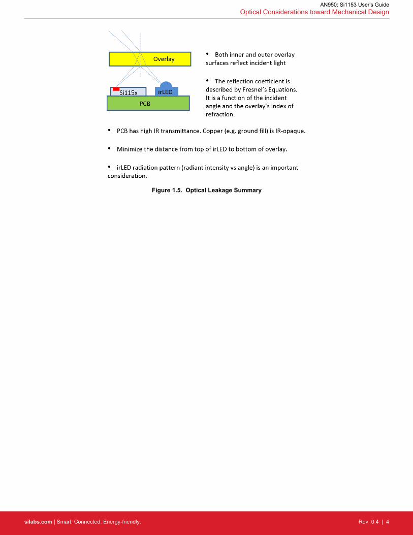
Figure 1.5. Optical Leakage Summary
AN950: Si1153 User's GuideOptical Considerations toward Mechanical Design
silabs.com | Smart. Connected. Energy-friendly. Rev. 0.4 | 4
1.3 Optical/Mechanical Components
1.3.1 Optical Blocking Material
A Si115x proximity system uses the “near infrared” wavelengths. As such, many objects that look black are candidates for optical block-ing material.
Natural Rubber is a common material known to be opaque to visible light and the near-infrared band. Another property of Natural Rub-ber that makes it suitable for optical blocking is its elasticity. Commercially-available rubber sheets can be cut to size for optical block-ing. For example:
http://www.rubbersheetroll.com/rubber-sheets.htm
Nitrile Rubber or “Buna-N” O-rings are used for optical blocking in Silicon Labs' evaluation platform and can be found at the followingweb site:
http://www.mcmaster.com/#4061t111/=9ujxqp
If an adhesive thin-sheet back device is desired, a polyurethane foam material from 3M (Bumpon™) can be used as an optical blockingmaterial:
http://www.digikey.com/product-search/en?vendor=0&keywords=bumpon%20roll
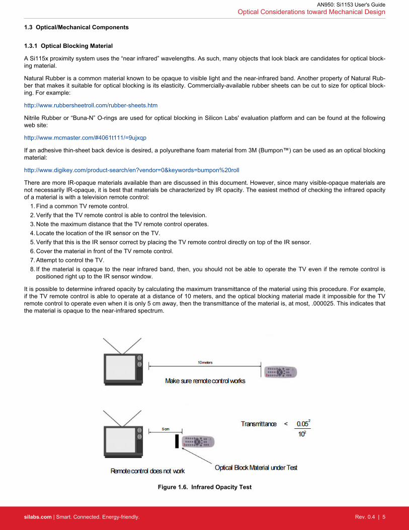
There are more IR-opaque materials available than are discussed in this document. However, since many visible-opaque materials arenot necessarily IR-opaque, it is best that materials be characterized by IR opacity. The easiest method of checking the infrared opacityof a material is with a television remote control:
1. Find a common TV remote control.2. Verify that the TV remote control is able to control the television.3. Note the maximum distance that the TV remote control operates.4. Locate the location of the IR sensor on the TV.5. Verify that this is the IR sensor correct by placing the TV remote control directly on top of the IR sensor.6. Cover the material in front of the TV remote control.7. Attempt to control the TV.8. If the material is opaque to the near infrared band, then, you should not be able to operate the TV even if the remote control is
positioned right up to the IR sensor window.
It is possible to determine infrared opacity by calculating the maximum transmittance of the material using this procedure. For example,if the TV remote control is able to operate at a distance of 10 meters, and the optical blocking material made it impossible for the TVremote control to operate even when it is only 5 cm away, then the transmittance of the material is, at most, .000025. This indicates thatthe material is opaque to the near-infrared spectrum.
Figure 1.6. Infrared Opacity Test
AN950: Si1153 User's GuideOptical Considerations toward Mechanical Design
silabs.com | Smart. Connected. Energy-friendly. Rev. 0.4 | 5
1.3.2 Infrared Properties of Printed Circuit Boards
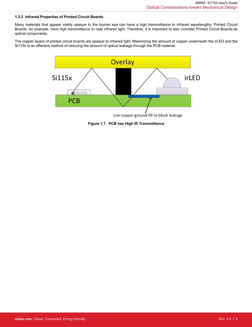
Many materials that appear visibly opaque to the human eye can have a high transmittance to infrared wavelengths. Printed CircuitBoards, for example, have high transmittance to near infrared light. Therefore, it is important to also consider Printed Circuit Boards asoptical components.
The copper layers of printed circuit boards are opaque to infrared light. Maximizing the amount of copper underneath the irLED and theSi115x is an effective method of reducing the amount of optical leakage through the PCB material.
Figure 1.7. PCB has High IR Transmittance
AN950: Si1153 User's GuideOptical Considerations toward Mechanical Design
silabs.com | Smart. Connected. Energy-friendly. Rev. 0.4 | 6
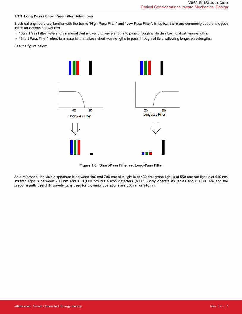
1.3.3 Long Pass / Short Pass Filter Definitions
Electrical engineers are familiar with the terms “High Pass Filter” and “Low Pass Filter”. In optics, there are commonly-used analogousterms for describing overlays.• “Long Pass Filter” refers to a material that allows long wavelengths to pass through while disallowing short wavelengths.• “Short Pass Filter” refers to a material that allows short wavelengths to pass through while disallowing longer wavelengths.
See the figure below.
Figure 1.8. Short-Pass Filter vs. Long-Pass Filter
As a reference, the visible spectrum is between 400 and 700 nm; blue light is at 430 nm; green light is at 550 nm; red light is at 640 nm.Infrared light is between 700 nm and > 10,000 nm but silicon detectors (si1153) only operate as far as about 1,000 nm and thepredominantly useful IR wavelengths used for proximity operations are 850 nm or 940 nm.
AN950: Si1153 User's GuideOptical Considerations toward Mechanical Design
silabs.com | Smart. Connected. Energy-friendly. Rev. 0.4 | 7

1.3.4 Optical Filter Characteristics of the Overlay
The Si115x does not require an optical filter for proper operation but one may be needed for additional performance or esthetic rea-sons. For the Si1153, there are two basic approaches when adding an optical filter:
1. IR Pass combined with moderate Visible attenuation (5% to 10% pass). This gives a dark look and allows both IR based proximityto work and ambient light sensing to work as well.
2. IR Pass combined with Visible blocking (< 2% pass). This gives a dark look and only allows IR based proximity to work. Ambientlight sensing does not work.
A “Long Pass Filter” with a corner wavelength of 700 nm attenuates visible light while allowing the infrared spectrum to pass through. Ingeneral, there is a esthetic desire for most products to hide internal electronics from visible view. Fortunately common materials andinks naturally have a higher transmittance to infrared light compared to visible light. This means that a painted overlay usually acts as a“long pass filter”. This does not mean that one should rely on the inks just “happening” to have the correct characteristics. “Long pass”inks are available with well-defined transmission characteristics,
In the case of a proximity sensing application, the “signal” is 850 nm or 940 nm infrared light emitted from the irLED. In a ProximitySense (PS) only application, if the overlay blocks everything except 850 nm ±30 nm, the system will operate.
In an ambient light application usage where there is a desire to measure the visible ambient light, the “signal” is light with a wavelengthof between 400 nm to 700 nm. From the perspective of an ambient light sensing application, any spectral reading above 700 nm andany spectral reading below 400 nm are “noise”. Attenuating the visible light to hide the internal electronics from view conflicts with theconcept of “maximizing the signal” for ALS usage BUT it allows the ambient light sensing to still function as long as a reasonableamount of light (~5% to 10%) is passed through the filter.
The optimal way to filter the visible light for ambient light sensing is to use a “bandpass filter” that is shaped in the form of a human eye.A filter with this response is called a “photopic” filter. When done correctly accuracies better than 10% can be achieved.
In the case of a combined proximity sensing and ambient light sensing application, Any attenuation of visible light must be moderate( 5% pass or better) while the IR should not be attenuated (e.g. > 70% pass).
The exact allowable attenuation numbers are dependent on customer requirements such as detectable low light levels and distancethat proximity must support.
In proximity applications, the “signal” is the light of the wavelength emitted from the irLED (e.g. 850 or 940 nm). If the transmittance atthe irLED wavelength is low, then much of the light from the irLED is absorbed by the overlay, leading to lower performance when itcomes to detecting more distant targets. Given the “target object distance” consideration, a significant optical overlay IR loss can trans-late to a loss in sensitivity with target object distance unless the overlay loss is compensated for with a more efficient irLED or higherirLED current. Note that the IR light used for proximity must pass through the overlay twice so that a poor 0.5 transmission yields a verypoor coupling factor of 0.5×0.5 = 0.25. For a proximity application, aside from aesthetic reasons or industrial design constraints, maxi-mizing the 850 nm or 940 nm transmittance should be the design goal. For applications requiring the highest performance under directsunlight the Si1153 parts with on die 940 nm filters provide the best performance.
The following links can be used for infrared applications:Teikoku MRX-HF IR Transmittable Black:
http://www.teikokuink.com/en/product/techreport/146_tech.html
Teikokuink’s GLS-HF 10415 SIL IR BLACK mix is especially recommended for tempered glass overlays forhigh-performance ALS and proximity applications using the Si115x.
Seiko Advance Ltd. IR Black Series:
http://www.seikoadvance.co.jp/en/products/category/category05.php
Nazdar Nazdar 6002050584 Special 84 IR:
https://sourceone.nazdar.com/portals/0/tds/NAZDAR_NSC61_IR_Transmitting_Black_Solvent-Based_Screen_Ink.pdf
EPOLIN Visible Opaque IR-Transmitting Screen Inks:
http://www.epolin.com/spectre%E2%84%A2-visibly-opaque-ir-transmitting-voirt-screen-inks
AN950: Si1153 User's GuideOptical Considerations toward Mechanical Design
silabs.com | Smart. Connected. Energy-friendly. Rev. 0.4 | 8
1.3.5 Overlay Characteristics and Choices
Clear acrylic material is generally available. A common trade name for acrylic sheet is “Plexiglass” and a Google search of that termtypically yields the most hits. Many web-based plastics companies offer acrylic sheets cut to custom sizes. In the U.S., the followingweb site has low-cost samples of clear acrylic sheets. Some polycarbonate samples are available through this web site as well: http://www.eplastics.com/Plastic/samples
Acrylic sheets are generally thicker than Polycarbonate sheets. If sheet thickness is an important consideration, polycarbonate is a bet-ter choice. The two main sources of polycarbonate resins are:
1. Lexan™ polycarbonate sheets:
http://www.sabic-ip.com/gep/Plastics/en/ProductsAndServices/ProductLine/lexan.html
http://www.sabic-ip.com/gep/Plastics/en/UtilityPages/ContactUs/contact_us_resins.html2. Bayer (Makrolon®) polycarbonate sheets:
http://www.plastics.covestro.com/en/Products/Makrolon
The following common overlay approaches are possible with the Si115x. They are listed in order of preference by performance.1. Clear plastic or glass overlay2. Clear overlay with ink applied through a silkscreen process3. Colored plastic or glass overlay
The choice of the overlay is often an industrial design decision. Many applications opt to start with a clear overlay material and screen-print the desired pattern using special inks.
Note that even if an overlay has a relatively low IR transmittance, this does not necessarily mean that the Si115x will not work with suchan overlay. The overlay transmittance is merely one of many system factors that come into play. For example, if the system must oper-ate under low IR transmittance overlays, then the following system-level tradeoffs include:• Reducing target object distance• Increase irLED current• Higher efficiency irLED• Narrower irLED half-angle
Typically, the irLED choice can compensate for overlay transmittance loss.
A common TV remote control can be used to determine the transmittance of the overlay material. Although the transmittance of the TVremote is at 940 nm, the ability of the overlay to pass 940 nm is close to its transmission at 850 nm.
Colored Overlay Considerations
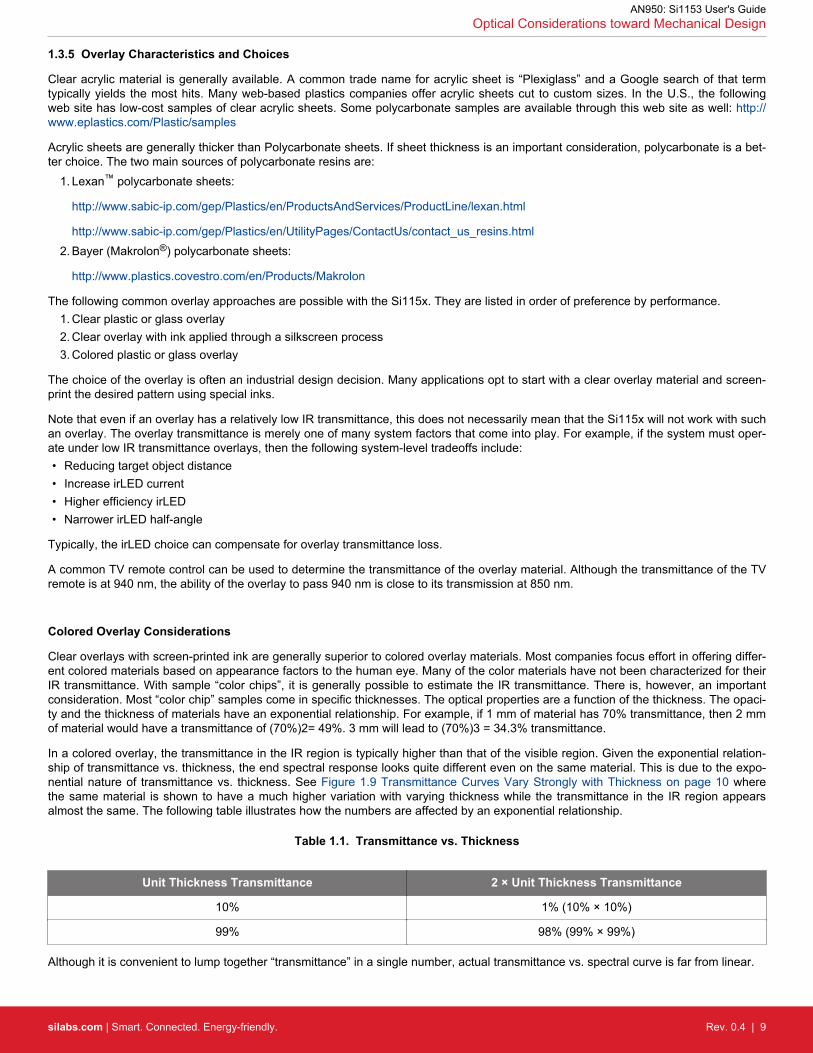
Clear overlays with screen-printed ink are generally superior to colored overlay materials. Most companies focus effort in offering differ-ent colored materials based on appearance factors to the human eye. Many of the color materials have not been characterized for theirIR transmittance. With sample “color chips”, it is generally possible to estimate the IR transmittance. There is, however, an importantconsideration. Most “color chip” samples come in specific thicknesses. The optical properties are a function of the thickness. The opaci-ty and the thickness of materials have an exponential relationship. For example, if 1 mm of material has 70% transmittance, then 2 mmof material would have a transmittance of (70%)2= 49%. 3 mm will lead to (70%)3 = 34.3% transmittance.
In a colored overlay, the transmittance in the IR region is typically higher than that of the visible region. Given the exponential relation-ship of transmittance vs. thickness, the end spectral response looks quite different even on the same material. This is due to the expo-nential nature of transmittance vs. thickness. See Figure 1.9 Transmittance Curves Vary Strongly with Thickness on page 10 wherethe same material is shown to have a much higher variation with varying thickness while the transmittance in the IR region appearsalmost the same. The following table illustrates how the numbers are affected by an exponential relationship.
Table 1.1. Transmittance vs. Thickness
Unit Thickness Transmittance 2 × Unit Thickness Transmittance
10% 1% (10% × 10%)
99% 98% (99% × 99%)
Although it is convenient to lump together “transmittance” in a single number, actual transmittance vs. spectral curve is far from linear.
AN950: Si1153 User's GuideOptical Considerations toward Mechanical Design
silabs.com | Smart. Connected. Energy-friendly. Rev. 0.4 | 9
Figure 1.9. Transmittance Curves Vary Strongly with Thickness
Coefficients calculated for a given colored overlay thickness may not apply for the same material of a different thickness. It is stronglyadvised that lux calculation coefficients be characterized only when a colored overlay of the proper thickness is available.
The other consequence is that high relative transmittance between the visible and IR portions of the spectrum can result in high ALSvariability. If ALS variation is an important system consideration, it may be advantageous to choose an overlay with a lower infraredtransmittance so that the infrared transmittance more closely matches that of the visible light transmittance. Doing so will allow lowerALS variation across different light sources. Choosing an overlay with a significant spectral difference in visible and IR generally leadsto higher ALS variance once the overlay thickness tolerance has been considered.
Information on Acrylic colored overlay samples can be found at the following web sites: http://www.eplastics.com/Plastic/samples
Information on Makrolon color chip samples can be found at the following URL (requires registration): http://www.plastics.covestro.com/Products/Color-Technologies.aspx
Information on Lexan color chip samples can be found at the following URL (requires registration): https://www.sabic-ip.com/cxp/ColorXPress
AN950: Si1153 User's GuideOptical Considerations toward Mechanical Design
silabs.com | Smart. Connected. Energy-friendly. Rev. 0.4 | 10
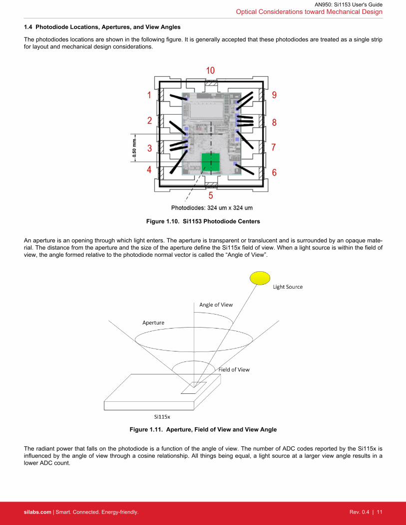
1.4 Photodiode Locations, Apertures, and View Angles
The photodiodes locations are shown in the following figure. It is generally accepted that these photodiodes are treated as a single stripfor layout and mechanical design considerations.
Figure 1.10. Si1153 Photodiode Centers
An aperture is an opening through which light enters. The aperture is transparent or translucent and is surrounded by an opaque mate-rial. The distance from the aperture and the size of the aperture define the Si115x field of view. When a light source is within the field ofview, the angle formed relative to the photodiode normal vector is called the “Angle of View”.
Figure 1.11. Aperture, Field of View and View Angle
The radiant power that falls on the photodiode is a function of the angle of view. The number of ADC codes reported by the Si115x isinfluenced by the angle of view through a cosine relationship. All things being equal, a light source at a larger view angle results in alower ADC count.
AN950: Si1153 User's GuideOptical Considerations toward Mechanical Design
silabs.com | Smart. Connected. Energy-friendly. Rev. 0.4 | 11
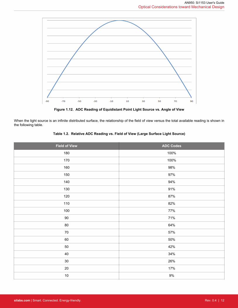
Figure 1.12. ADC Reading of Equidistant Point Light Source vs. Angle of View
When the light source is an infinite distributed surface, the relationship of the field of view versus the total available reading is shown inthe following table.
Table 1.2. Relative ADC Reading vs. Field of View (Large Surface Light Source)
Field of View ADC Codes
180 100%
170 100%
160 98%
150 97%
140 94%
130 91%
120 87%
110 82%
100 77%
90 71%
80 64%
70 57%
60 50%
50 42%
40 34%
30 26%
20 17%
10 9%
AN950: Si1153 User's GuideOptical Considerations toward Mechanical Design
silabs.com | Smart. Connected. Energy-friendly. Rev. 0.4 | 12
If the target object is small (smaller than the field of view), the ADC codes reported by the Si115x are influenced by the angle of view.The field of view only needs to be as big as the expected location of the target. An example of such an application is a 50 cm rangewhere the angle subtended by the target object is small compared to the field of view.
If the target object is large (larger than the field of view), the amount of light received by the Si115x is influenced by the field of view. Anexample application is the cell-phone cheek detector; the cheek represents a large object due to its location relative to the sensor. Forthis case, maximizing the field of view is important. For these applications, a field of view of 120 ° is recommended. This means that, forbest performance, the aperture either needs to be large or near the Si115x. By increasing the aperture, the greatest amount of light canenter the Si115x, and less light needs to be thrown at the target object, leading to a more efficient design.
1.5 Close Range Application with Single-Port Topology
Single-Port design is not recommended for general proximity applications. The performance will degrade due to the lack of opticalblocking. Unless low cost is the primary objective of the system design, Dual-Port or Hybrid topology should always be the first choice.
This section and 1.6 Single-Port Design Dimensions apply only to Single-Port topology when the target is close. For systems that em-ploy optical blocking or a Dual-Port topology, the optical leakage is controlled through the optical blocking material. In a Single-Porttopology, geometry is the primary method of limiting the optical leakage.
1.5.1 IrLED Choice
The irLED chosen for this must have a half-angle of 22° or less. As described in 1.3 Optical/Mechanical Components, light power thatdoes not exit the system generally ends up fueling optical leakage through secondary leakage paths. Choosing a low half-angle irLEDcauses much of the light power to be directed outside the system, resulting in lower optical leakage.
Another important consideration of the irLED is that it must be as tall as the product’s construction will allow. By choosing a tall irLED,the irLED will be nearer the overlay. Having the irLED near the overlay causes most of the light to go outside the system rather thanbeing reflected back in and causing higher levels of optical leakage.
The Si1153 Evaluation Platforms use the Osram SFH 4056. Many of these recommendations can also apply to other irLEDs as long asthe radiation pattern is narrower than 22°.
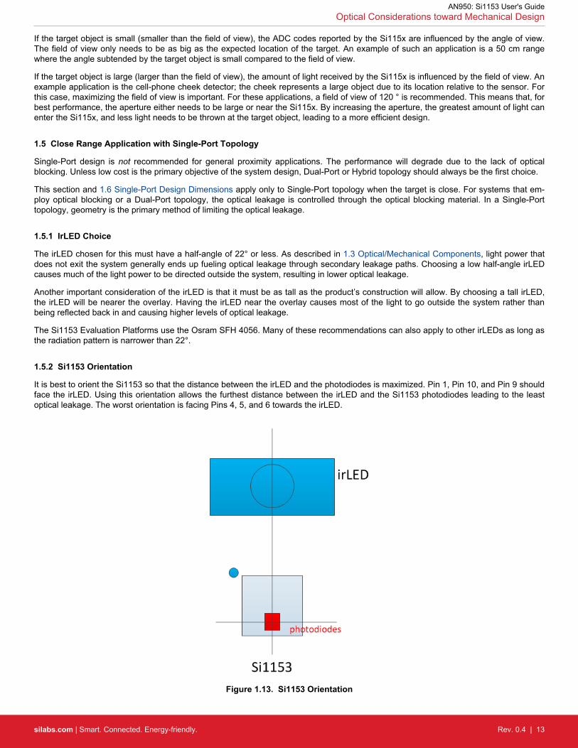
1.5.2 Si1153 Orientation
It is best to orient the Si1153 so that the distance between the irLED and the photodiodes is maximized. Pin 1, Pin 10, and Pin 9 shouldface the irLED. Using this orientation allows the furthest distance between the irLED and the Si1153 photodiodes leading to the leastoptical leakage. The worst orientation is facing Pins 4, 5, and 6 towards the irLED.
Figure 1.13. Si1153 Orientation
AN950: Si1153 User's GuideOptical Considerations toward Mechanical Design
silabs.com | Smart. Connected. Energy-friendly. Rev. 0.4 | 13
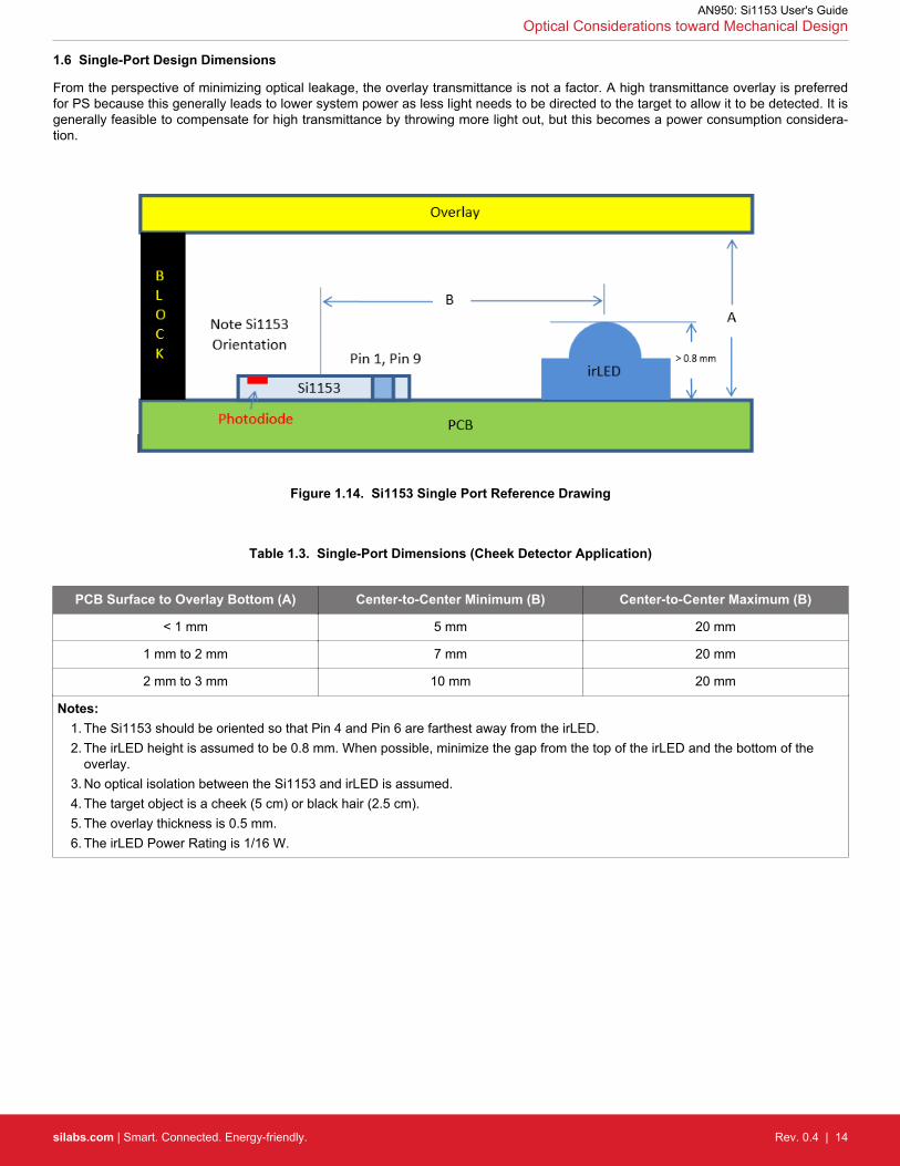
1.6 Single-Port Design Dimensions
From the perspective of minimizing optical leakage, the overlay transmittance is not a factor. A high transmittance overlay is preferredfor PS because this generally leads to lower system power as less light needs to be directed to the target to allow it to be detected. It isgenerally feasible to compensate for high transmittance by throwing more light out, but this becomes a power consumption considera-tion.
Figure 1.14. Si1153 Single Port Reference Drawing
Table 1.3. Single-Port Dimensions (Cheek Detector Application)
PCB Surface to Overlay Bottom (A) Center-to-Center Minimum (B) Center-to-Center Maximum (B)
< 1 mm 5 mm 20 mm
1 mm to 2 mm 7 mm 20 mm
2 mm to 3 mm 10 mm 20 mm
Notes:1. The Si1153 should be oriented so that Pin 4 and Pin 6 are farthest away from the irLED.2. The irLED height is assumed to be 0.8 mm. When possible, minimize the gap from the top of the irLED and the bottom of the
overlay.3. No optical isolation between the Si1153 and irLED is assumed.4. The target object is a cheek (5 cm) or black hair (2.5 cm).5. The overlay thickness is 0.5 mm.6. The irLED Power Rating is 1/16 W.
AN950: Si1153 User's GuideOptical Considerations toward Mechanical Design
silabs.com | Smart. Connected. Energy-friendly. Rev. 0.4 | 14
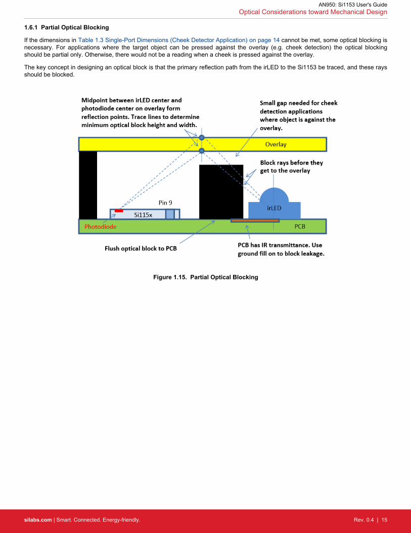
1.6.1 Partial Optical Blocking
If the dimensions in Table 1.3 Single-Port Dimensions (Cheek Detector Application) on page 14 cannot be met, some optical blocking isnecessary. For applications where the target object can be pressed against the overlay (e.g. cheek detection) the optical blockingshould be partial only. Otherwise, there would not be a reading when a cheek is pressed against the overlay.
The key concept in designing an optical block is that the primary reflection path from the irLED to the Si1153 be traced, and these raysshould be blocked.
Figure 1.15. Partial Optical Blocking
AN950: Si1153 User's GuideOptical Considerations toward Mechanical Design
silabs.com | Smart. Connected. Energy-friendly. Rev. 0.4 | 15
1.7 Long Range Applications
If the target is small or far away, the Si1153 may need to operate at a higher ADC sensitivity setting. This is accomplished throughincreasing the HW_GAIN setting. When increasing the HW_GAIN setting, both reflectance and optical leakage are magnified. To allowoperation at the highest possible ADC sensitivity, the optical leakage should be kept low so as possible.
The limitation to how high the HW_GAIN setting can be set is a function of the following:• Ambient IR• Optical Leakage
The IR ambient can be controlled through the following methods:1. Limiting field of view by using a smaller Aperture (see 1.4 Photodiode Locations, Apertures, and View Angles).2. Limiting field of view by using lenses3. Using special overlays, such as a Visible Light Blocking Overlay (Long pass Filters) when CFL/Fluorescent lighting is the predomi-
nant lighting condition.
In general, the Dual Port topology provides the lowest leakage. The Hybrid approach can be used as long as proper optical blocking isused.
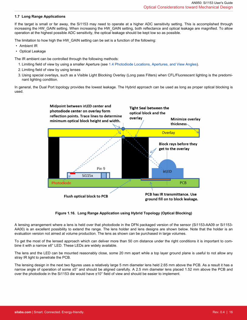
Figure 1.16. Long Range Application using Hybrid Topology (Optical Blocking)
A lensing arrangement where a lens is held over that photodiode in the DFN packaged version of the sensor (Si1153-AA09 or Si1153-AA00) is an excellent possibility to extend the range. The lens holder and lens designs are shown below. Note that the holder is anevaluation version not aimed at volume production. The lens as shown can be purchased in large volumes.
To get the most of the lensed approach which can deliver more than 50 cm distance under the right conditions it is important to com-bine it with a narrow ±6° LED. These LEDs are widely available.
The lens and the LED can be mounted reasonably close, some 20 mm apart while a top layer ground plane is useful to not allow anystray IR light to penetrate the PCB.
The lensing design in the next two figures uses a relatively large 5 mm diameter lens held 2.65 mm above the PCB. As a result it has anarrow angle of operation of some ±5° and should be aligned carefully. A 2.5 mm diameter lens placed 1.52 mm above the PCB andover the photodiode in the Si1153 die would have ±10° field of view and should be easier to implement.
AN950: Si1153 User's GuideOptical Considerations toward Mechanical Design
silabs.com | Smart. Connected. Energy-friendly. Rev. 0.4 | 16

Figure 1.17. Evaluation Example of a Lens Holder for Distance Proximity
AN950: Si1153 User's GuideOptical Considerations toward Mechanical Design
silabs.com | Smart. Connected. Energy-friendly. Rev. 0.4 | 17
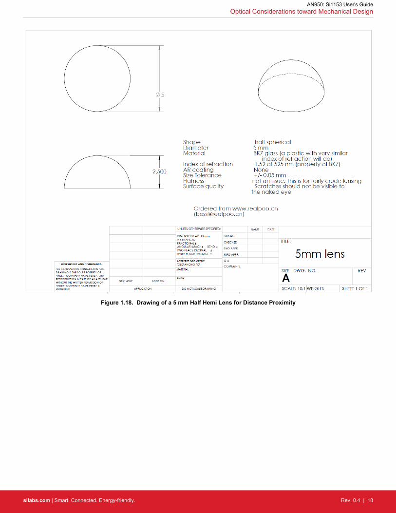
Figure 1.18. Drawing of a 5 mm Half Hemi Lens for Distance Proximity
AN950: Si1153 User's GuideOptical Considerations toward Mechanical Design
silabs.com | Smart. Connected. Energy-friendly. Rev. 0.4 | 18
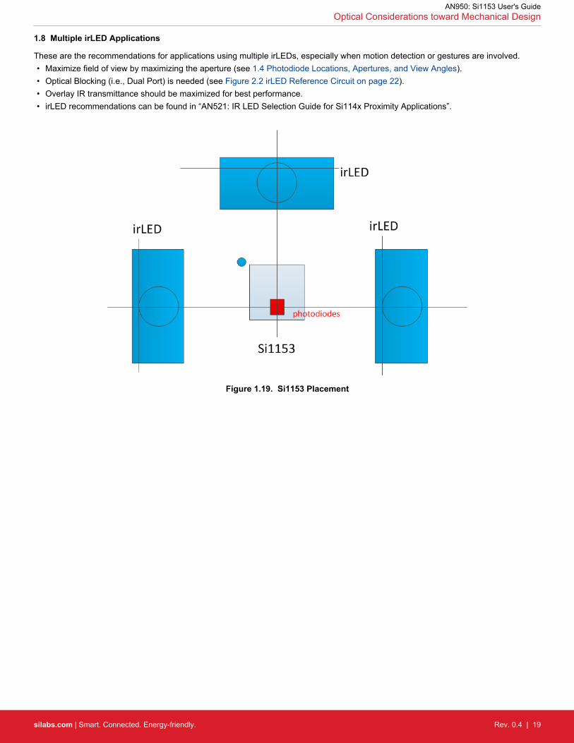
1.8 Multiple irLED Applications
These are the recommendations for applications using multiple irLEDs, especially when motion detection or gestures are involved.• Maximize field of view by maximizing the aperture (see 1.4 Photodiode Locations, Apertures, and View Angles).• Optical Blocking (i.e., Dual Port) is needed (see Figure 2.2 irLED Reference Circuit on page 22).• Overlay IR transmittance should be maximized for best performance.• irLED recommendations can be found in “AN521: IR LED Selection Guide for Si114x Proximity Applications”.
Figure 1.19. Si1153 Placement
AN950: Si1153 User's GuideOptical Considerations toward Mechanical Design
silabs.com | Smart. Connected. Energy-friendly. Rev. 0.4 | 19
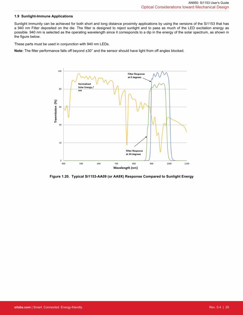
1.9 Sunlight-Immune Applications
Sunlight immunity can be achieved for both short and long distance proximity applications by using the versions of the Si1153 that hasa 940 nm Filter deposited on the die. The filter is designed to reject sunlight and to pass as much of the LED excitation energy aspossible. 940 nm is selected as the operating wavelength since it corresponds to a dip in the energy of the solar spectrum, as shown inthe figure below.
These parts must be used in conjunction with 940 nm LEDs.
Note: The filter performance falls off beyond ±30° and the sensor should have light from off angles blocked.
Figure 1.20. Typical Si1153-AA09 (or AA9X) Response Compared to Sunlight Energy
AN950: Si1153 User's GuideOptical Considerations toward Mechanical Design
silabs.com | Smart. Connected. Energy-friendly. Rev. 0.4 | 20

2. Electrical Component Selection
2.1 Typical Application Schematic Diagrams
The following figure shows a schematic of the Si1153 for basic applications.
Figure 2.1. Si1153 Schematic Diagrams
2.2 Mandatory LED3 Pull-Up Resistor
This section applies to the 47 kΩ pull-up resistor from the LED3 pin to VDD. Refer to Figure 2.1 Si1153 Schematic Diagrams on page21.
Upon reset, the LED3 pin operates as a factory test pin to the internal microcontroller. Under this boot-up condition, if the LED3 pin isnot pulled-up to VDD, the Si1153 does not come out of reset.
To determine if the resistor is needed, it is necessary to calculate the difference between the VLED and VDD voltage rails and ensurethat this difference is greater than the forward drop of the irLED under its leakage condition. The resistor can be removed if the VLEDrail is high enough relative to the VDD rail.
If there is uncertainty whether the resistor is needed, it is recommended that a pad site be left on the PCB until this determination hasbeen made.
The following symptoms can occur when the LED3 pins are not high during boot:• The device does not communicate.• Some parts can communicate; some parts do not communicate.• Since there is a floating node, “non-booting” devices may begin to boot with temperature or ambient light changes.
AN950: Si1153 User's GuideElectrical Component Selection
silabs.com | Smart. Connected. Energy-friendly. Rev. 0.4 | 21
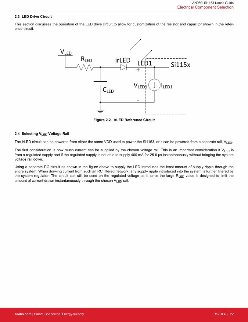
2.3 LED Drive Circuit
This section discusses the operation of the LED drive circuit to allow for customization of the resistor and capacitor shown in the refer-ence circuit.
Figure 2.2. irLED Reference Circuit
2.4 Selecting VLED Voltage Rail
The irLED circuit can be powered from either the same VDD used to power the Si1153, or it can be powered from a separate rail, VLED.
The first consideration is how much current can be supplied by the chosen voltage rail. This is an important consideration if VLED isfrom a regulated supply and if the regulated supply is not able to supply 400 mA for 25.6 µs instantaneously without bringing the systemvoltage rail down.
Using a separate RC circuit as shown in the figure above to supply the LED introduces the least amount of supply ripple through theentire system. When drawing current from such an RC filtered network, any supply ripple introduced into the system is further filtered bythe system regulator. The circuit can still be used on the regulated voltage as-is since the large RLED value is designed to limit theamount of current drawn instantaneously through the chosen VLED rail.
AN950: Si1153 User's GuideElectrical Component Selection
silabs.com | Smart. Connected. Energy-friendly. Rev. 0.4 | 22
2.5 Selecting CLED
Ideally, the CLED should possess sufficient capacitance to store enough charge for each of the measurements. This can be achieved byusing the following equation:
CLED = Number of LEDs × Max ir LED Current × 24.4μs × 2(HW_GAIN )
V LED − V f − 0.5
The Si1153 contains six measurement channels and makes up to six measurements before going back to sleep.
Since these six measurements are done in a very short time, the capacitor does not have much time to charge back up.
In the example below, the irLED current chosen for each of these channels is 360 mA.
VF is the forward voltage dropped by the irLED at 360 mA. This is typically derived from looking at a data sheet of the irLED.
For example, an OSRAM SFH 4056 irLED drops around 2.2 V at 360 mA.
The default HW_GAIN is zero. 20 is 1.
In this example, assume that the VLED chosen is 4.3 V.
RLED < Time between Proximity MeasurementsCLED × 5
This means that, if CLED is 16 µF or more, there is sufficient charge stored within the capacitor to allow current to flow through theirLED. With this capacitor, there is not any significant current drawn from the system in the 24.4 µs period when the irLEDs are beingdriven.
2.6 Selecting RLED
As long as the capacitor, CLED, is able to provide enough charge to supply the current needed for the irLEDs, the RLED resistor general-ly has two functions:• Minimizes instantaneous current drawn from the voltage rail• Charges up the CLED capacitor.
When in this role, the design constraint is to make sure that the CLED capacitor is fully charged by the time the next set of proximitymeasurements is made.
RLED < Time between Proximity MeasurementsCLED × 5
If the CLED capacitor chosen is too small, it may be necessary to draw more current from the VDD supply to provide supplementarycurrent so that the capacitor does not discharge before reaching an excessively low voltage.
For this case, the RLED should be smaller to supply instantaneous current from the VLED rail. For example, to be able to continuouslysupply 360 mA using an irLED with a 2.2 V forward drop:
RLED <(V LED − 2.2 − 0.5)
0.360
In this case, the system must be able to supply a peak instantaneous current of 360 mA. The charge stored in the capacitor reduces theamount of time the system draws from the VLED rail, but, in the end, the current needs to be sourced through the resistor.
Due to the low duty cycle of the current pulses, the power rating of the resistor does not need to be very high since little heating isexpected. A low-cost 1/16 W resistor can be used.
AN950: Si1153 User's GuideElectrical Component Selection
silabs.com | Smart. Connected. Energy-friendly. Rev. 0.4 | 23

2.7 irLED Electrical Considerations
This section only refers to electrical considerations when choosing an irLED. Optical considerations are not discussed here.
The Si1153 attempts to sink a constant current through the irLED. The irLED should be examined for the following parameters:• Forward voltage VF
• 360 mA capability
An irLED with a lower VF is preferred. With a lower forward voltage, the voltage across CLED can be charged to a higher value, allowingmore charge to be stored. This may lead to a smaller CLED, especially when the VLED rail is relatively low.
If the irLED can operate at 360 mA, by default, the Si1153 pulses the irLED for 24.4 µs. However, this pulse width is host-programma-ble through HW_GAIN and can be much higher.
AN950: Si1153 User's GuideElectrical Component Selection
silabs.com | Smart. Connected. Energy-friendly. Rev. 0.4 | 24
3. Proximity Measurements
3.1 Ambient IR, Optical Leakage, and Target Reflectance
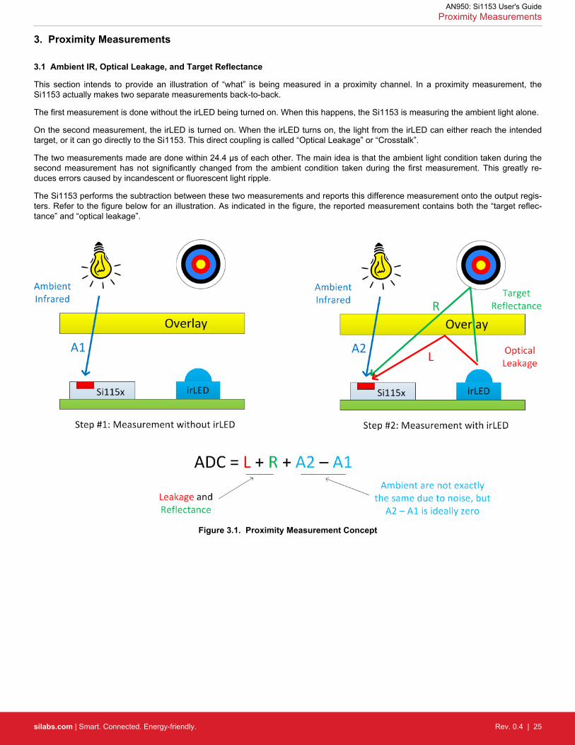
This section intends to provide an illustration of “what” is being measured in a proximity channel. In a proximity measurement, theSi1153 actually makes two separate measurements back-to-back.
The first measurement is done without the irLED being turned on. When this happens, the Si1153 is measuring the ambient light alone.
On the second measurement, the irLED is turned on. When the irLED turns on, the light from the irLED can either reach the intendedtarget, or it can go directly to the Si1153. This direct coupling is called “Optical Leakage” or “Crosstalk”.
The two measurements made are done within 24.4 µs of each other. The main idea is that the ambient light condition taken during thesecond measurement has not significantly changed from the ambient condition taken during the first measurement. This greatly re-duces errors caused by incandescent or fluorescent light ripple.
The Si1153 performs the subtraction between these two measurements and reports this difference measurement onto the output regis-ters. Refer to the figure below for an illustration. As indicated in the figure, the reported measurement contains both the “target reflec-tance” and “optical leakage”.
Figure 3.1. Proximity Measurement Concept
AN950: Si1153 User's GuideProximity Measurements
silabs.com | Smart. Connected. Energy-friendly. Rev. 0.4 | 25
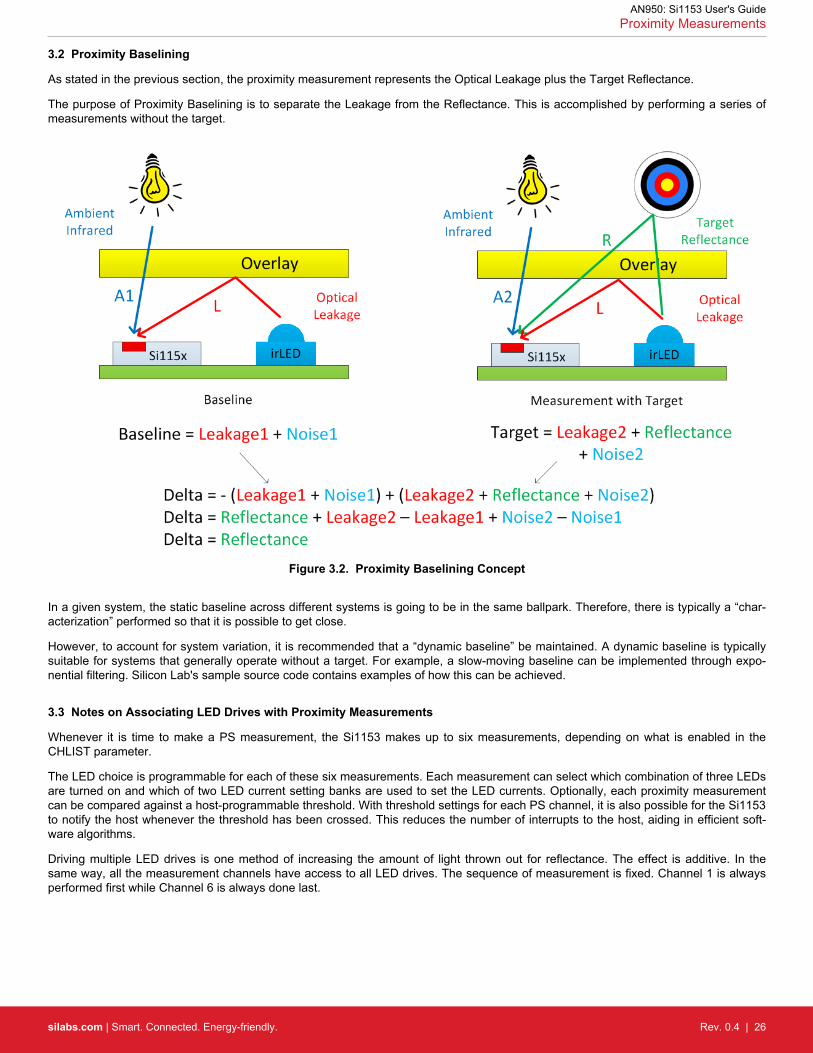
3.2 Proximity Baselining
As stated in the previous section, the proximity measurement represents the Optical Leakage plus the Target Reflectance.
The purpose of Proximity Baselining is to separate the Leakage from the Reflectance. This is accomplished by performing a series ofmeasurements without the target.
Figure 3.2. Proximity Baselining Concept
In a given system, the static baseline across different systems is going to be in the same ballpark. Therefore, there is typically a “char-acterization” performed so that it is possible to get close.
However, to account for system variation, it is recommended that a “dynamic baseline” be maintained. A dynamic baseline is typicallysuitable for systems that generally operate without a target. For example, a slow-moving baseline can be implemented through expo-nential filtering. Silicon Lab's sample source code contains examples of how this can be achieved.
3.3 Notes on Associating LED Drives with Proximity Measurements
Whenever it is time to make a PS measurement, the Si1153 makes up to six measurements, depending on what is enabled in theCHLIST parameter.
The LED choice is programmable for each of these six measurements. Each measurement can select which combination of three LEDsare turned on and which of two LED current setting banks are used to set the LED currents. Optionally, each proximity measurementcan be compared against a host-programmable threshold. With threshold settings for each PS channel, it is also possible for the Si1153to notify the host whenever the threshold has been crossed. This reduces the number of interrupts to the host, aiding in efficient soft-ware algorithms.
Driving multiple LED drives is one method of increasing the amount of light thrown out for reflectance. The effect is additive. In thesame way, all the measurement channels have access to all LED drives. The sequence of measurement is fixed. Channel 1 is alwaysperformed first while Channel 6 is always done last.
AN950: Si1153 User's GuideProximity Measurements
silabs.com | Smart. Connected. Energy-friendly. Rev. 0.4 | 26
3.4 Minimizing the Effect of Ambient-Light Ripple
During proximity detection, the Si1153 cancels ambient light by subtracting the results of two measurements. The first measurementsenses ambient light alone with the IRLED turned off. The second measurement is made with the IRLED turned on, thus sensing boththe proximity signal and ambient light. This cancellation method works well if the ambient light does not change between measure-ments.
However, most light sources have a certain amount of ripple. For incandescent bulbs powered by the mains, the light level fluctuates at100 or 120 Hz, depending on the mains frequency. Fluorescent bulbs fluctuate at lower amplitudes than incandescent bulbs, but atfrequencies in the tens of kilohertz.
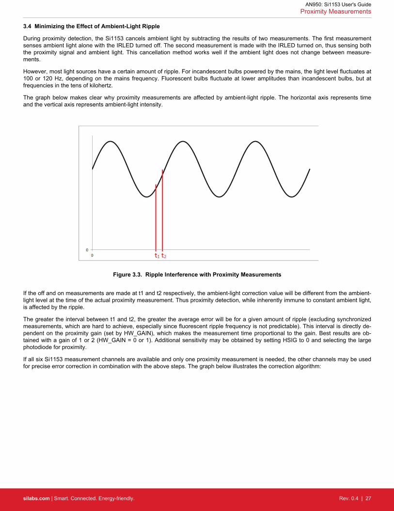
The graph below makes clear why proximity measurements are affected by ambient-light ripple. The horizontal axis represents timeand the vertical axis represents ambient-light intensity.
Figure 3.3. Ripple Interference with Proximity Measurements
If the off and on measurements are made at t1 and t2 respectively, the ambient-light correction value will be different from the ambient-light level at the time of the actual proximity measurement. Thus proximity detection, while inherently immune to constant ambient light,is affected by the ripple.
The greater the interval between t1 and t2, the greater the average error will be for a given amount of ripple (excluding synchronizedmeasurements, which are hard to achieve, especially since fluorescent ripple frequency is not predictable). This interval is directly de-pendent on the proximity gain (set by HW_GAIN), which makes the measurement time proportional to the gain. Best results are ob-tained with a gain of 1 or 2 (HW_GAIN = 0 or 1). Additional sensitivity may be obtained by setting HSIG to 0 and selecting the largephotodiode for proximity.
If all six Si1153 measurement channels are available and only one proximity measurement is needed, the other channels may be usedfor precise error correction in combination with the above steps. The graph below illustrates the correction algorithm:
AN950: Si1153 User's GuideProximity Measurements
silabs.com | Smart. Connected. Energy-friendly. Rev. 0.4 | 27
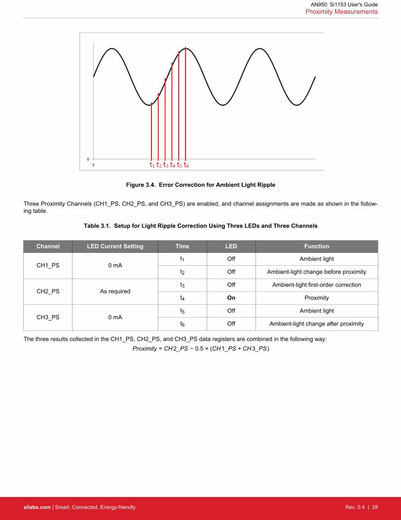
Figure 3.4. Error Correction for Ambient Light Ripple
Three Proximity Channels (CH1_PS, CH2_PS, and CH3_PS) are enabled, and channel assignments are made as shown in the follow-ing table.
Table 3.1. Setup for Light Ripple Correction Using Three LEDs and Three Channels
Channel LED Current Setting Time LED Function
CH1_PS 0 mAt1 Off Ambient light
t2 Off Ambient-light change before proximity
CH2_PS As requiredt3 Off Ambient-light first-order correction
t4 On Proximity
CH3_PS 0 mAt5 Off Ambient light
t6 Off Ambient-light change after proximity
The three results collected in the CH1_PS, CH2_PS, and CH3_PS data registers are combined in the following way:Proximity = CH 2_PS − 0.5 × (CH 1_PS + CH 3_PS )
AN950: Si1153 User's GuideProximity Measurements
silabs.com | Smart. Connected. Energy-friendly. Rev. 0.4 | 28
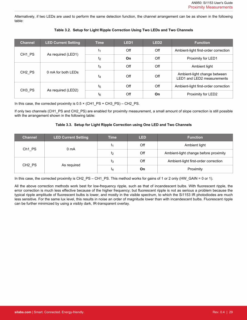
Alternatively, if two LEDs are used to perform the same detection function, the channel arrangement can be as shown in the followingtable:
Table 3.2. Setup for Light Ripple Correction Using Two LEDs and Two Channels
Channel LED Current Setting Time LED1 LED2 Function
CH1_PS As required (LED1)t1 Off Off Ambient-light first-order correction
t2 On Off Proximity for LED1
CH2_PS 0 mA for both LEDs
t3 Off Off Ambient light
t4 Off Off Ambient-light change betweenLED1 and LED2 measurements
CH3_PS As required (LED2)t5 Off Off Ambient-light first-order correction
t6 Off On Proximity for LED2
In this case, the corrected proximity is 0.5 × (CH1_PS + CH3_PS) – CH2_PS.
If only two channels (CH1_PS and CH2_PS) are enabled for proximity measurement, a small amount of slope correction is still possiblewith the arrangement shown in the following table:
Table 3.3. Setup for Light Ripple Correction using One LED and Two Channels
Channel LED Current Setting Time LED Function
Ch1_PS 0 mAt1 Off Ambient light
t2 Off Ambient-light change before proximity
CH2_PS As requiredt3 Off Ambient-light first-order correction
t4 On Proximity
In this case, the corrected proximity is CH2_PS – CH1_PS. This method works for gains of 1 or 2 only (HW_GAIN = 0 or 1).
All the above correction methods work best for low-frequency ripple, such as that of incandescent bulbs. With fluorescent ripple, theerror correction is much less effective because of the higher frequency; but fluorescent ripple is not as serious a problem because thetypical ripple amplitude of fluorescent bulbs is lower, and mostly in the visible spectrum, to which the Si1153 IR photodiodes are muchless sensitive. For the same lux level, this results in noise an order of magnitude lower than with incandescent bulbs. Fluorescent ripplecan be further minimized by using a visibly dark, IR-transparent overlay.
AN950: Si1153 User's GuideProximity Measurements
silabs.com | Smart. Connected. Energy-friendly. Rev. 0.4 | 29
4. Programming Guide
This guide provides information that is suplemental to the data sheet. For a full description of the registers and bit fields, refer to theSi1153 Data Sheet.
4.1 Minimum Initialization Code (Pseudo Code)
Upon reset, the minimum code necessary to obtain measurements out of each optical channel is shown. Note that many of the definesare in the file called Si1153_defs.h. It is recommended that the symbols within the files be used so that the code is more readable.
The following code uses hardware-independent functions for I2C communication that the user must provide.
U8 Si115xReadFromRegister (U8 reg); returns byte from I2C Register 'reg'void Si115xWriteToRegister (U8 reg, U8 value); writes 'value' into I2C Register reg'void Si115xParamSet (U8 address, U8 value); writes 'value' into Parameter 'address'Si115xForce(); equivalent to Si115xWriteToRegister (REG_COMMAND, 0x11) This forces enabled channels’ measurements
// Enable 3 channels for proximity measurementSi115xParamSet( si115x_handle, PARAM_CH_LIST, 0x07);
// Initialize LED currentSi115xParamSet( si115x_handle, PARAM_LED1_A, 0x3f);Si115xParamSet( si115x_handle, PARAM_LED2_A, 0x3f);Si115xParamSet( si115x_handle, PARAM_LED3_A, 0x3f);
// Configure ADC and enable LED driveSi115xParamSet( si115x_handle, PARAM_ADCCONFIG0, 0x62);Si115xParamSet( si115x_handle, PARAM_MEASCONFIG0, 0x01);Si115xParamSet( si115x_handle, PARAM_ADCCONFIG1, 0x62);Si115xParamSet( si115x_handle, PARAM_MEASCONFIG1, 0x02);Si115xParamSet( si115x_handle, PARAM_ADCCONFIG2, 0x62);Si115xParamSet( si115x_handle, PARAM_MEASCONFIG2, 0x04);
// Enable InterruptSi115xWriteToRegister( si115x_handle, REG_IRQ_ENABLE, 0x07);
// Start Force measurementSi115xForce();
// Once the measurements are completed, an interrupt will be generated to the host// Here is how the host should reconstruct the sample in IRQ// Note very carefully that 16-bit registers are in the 'Big Endian' byte order// It will be more efficient to perform I2C Burst Reads, but this example shows// individual reads of registers
CH1_PS = Si115xReadFromRegister (REG_HOSTOUT1) + 256 * Si115xReadFromRegister (REG_HOSTOUT0);CH2_PS = Si115xReadFromRegister (REG_HOSTOUT3) + 256 * Si115xReadFromRegister (REG_HOSTOUT2);CH3_PS = Si115xReadFromRegister (REG_HOSTOUT5) + 256 * Si115xReadFromRegister (REG_HOSTOUT4);
Be aware of the Big-endian ordering when constructing the 16-bit variable.
The sample code is also available in the Programmer’s Toolkit which can be downloaded and installed from Silicon Labs website.
AN950: Si1153 User's GuideProgramming Guide
silabs.com | Smart. Connected. Energy-friendly. Rev. 0.4 | 30
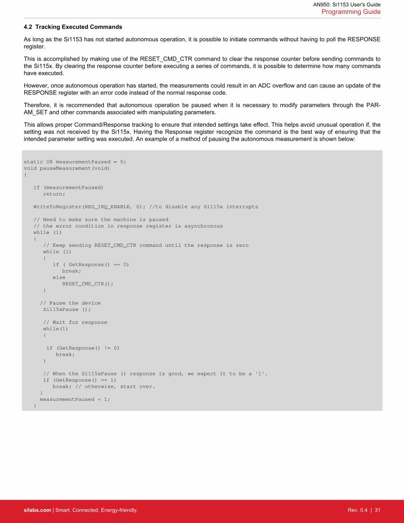
4.2 Tracking Executed Commands
As long as the Si1153 has not started autonomous operation, it is possible to initiate commands without having to poll the RESPONSEregister.
This is accomplished by making use of the RESET_CMD_CTR command to clear the response counter before sending commands tothe Si115x. By clearing the response counter before executing a series of commands, it is possible to determine how many commandshave executed.
However, once autonomous operation has started, the measurements could result in an ADC overflow and can cause an update of theRESPONSE register with an error code instead of the normal response code.
Therefore, it is recommended that autonomous operation be paused when it is necessary to modify parameters through the PAR-AM_SET and other commands associated with manipulating parameters.
This allows proper Command/Response tracking to ensure that intended settings take effect. This helps avoid unusual operation if, thesetting was not received by the Si115x. Having the Response register recognize the command is the best way of ensuring that theintended parameter setting was executed. An example of a method of pausing the autonomous measurement is shown below:
static U8 measurementPaused = 0;void pauseMeasurement(void){
if (measurementPaused) return;
WriteToRegister(REG_IRQ_ENABLE, 0); //to disable any Si115x interrupts
// Need to make sure the machine is paused // the error condition in response register is asynchronous while (1) { // Keep sending RESET_CMD_CTR command until the response is zero while (1) { if ( GetResponse() == 0) break; else RESET_CMD_CTR(); }
// Pause the device Si115xPause ();
// Wait for response while(1) {
if (GetResponse() != 0) break; }
// When the Si115xPause () response is good, we expect it to be a '1'. if (GetResponse() == 1) break; // otherwise, start over. } measurementPaused = 1; }
AN950: Si1153 User's GuideProgramming Guide
silabs.com | Smart. Connected. Energy-friendly. Rev. 0.4 | 31

An example of a method of resuming an autonomous measurement is shown in the following code.
void resumeMeasurement(void){
if (!measurementPaused) return;
ClearIrqStatus(); Si115xWriteToRegister( si115x_handle, REG_IRQ_ENABLE, 0x07); // re-enables INTSi115xStart ();measurementPaused = 0;}
4.3 Resetting the Si1153
The Si1153 has an internal microcontroller. When the Si1153 receives a RESET_SW command from the host (The I2C Command Reg-ister is written with 0x01), the Si1153 controller initiates an internal hardware reset.
This reset command is intended to place the Si1153 in its hardware reset state. If the reset command is initiated, prior initializationsteps need to be repeated.
The Reset Command is used with Silicon Labs Evaluation Systems for a specific reason. In Silicon Lab's Evaluation Systems, the hostcontroller driving the Si1153 contains flash memory. As it is a development environment, the flash memory can be reprogrammedthrough the Integrated Development Environment.
When the host controller goes through a flash memory reprogram cycle and resets, the Si1153 is unaware of this event. Therefore, ifthe Si1153 is already performing autonomous measurements, the Si1153 does not know that it is supposed to stop.
On the other hand, after the host controller has been reprogrammed, it does not know whether the Si1153 is already performing auton-omous measurements from a prior context. Therefore, the example code in the Si1153 Evaluation Systems generally shows a resetsequence performed at the very beginning of the Si1153 initialization sequence. If both the Si1153x and the host always operate from apower-on-reset sequence, the reset command does not need to be issued.
The reset command is useful in a system watchdog. If the software system has a watchdog looking for catastrophic errors, it is general-ly a good idea to include a Si1153 reset sequence as part of the recovery.
The reset command, when used in the middle of other initialization settings, is not recommended. All settings prior to the Si1153 resetcommand are lost.
AN950: Si1153 User's GuideProgramming Guide
silabs.com | Smart. Connected. Energy-friendly. Rev. 0.4 | 32
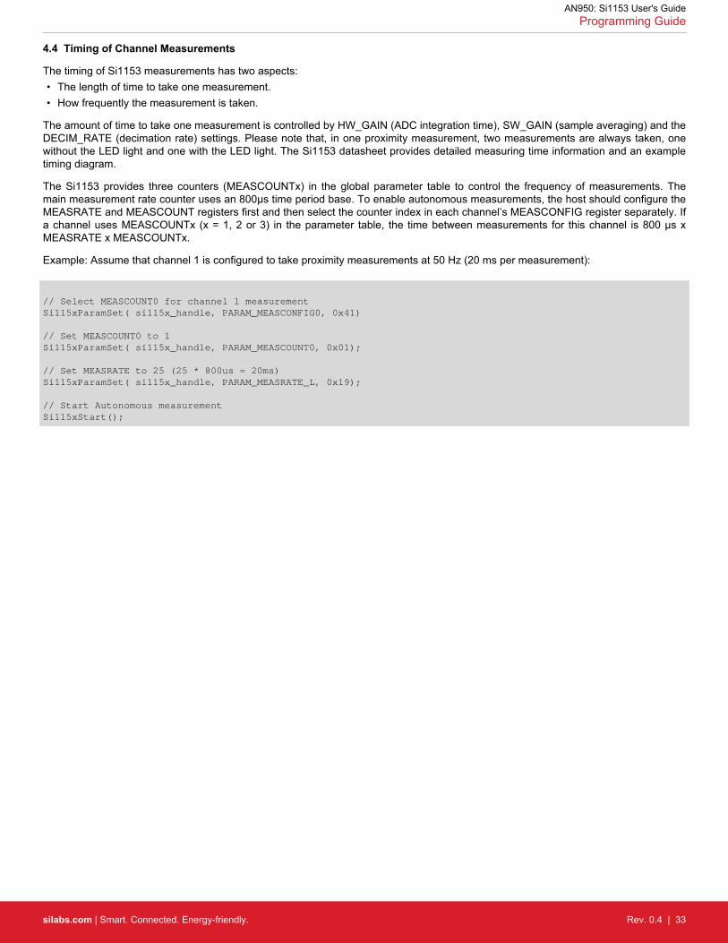
4.4 Timing of Channel Measurements
The timing of Si1153 measurements has two aspects:• The length of time to take one measurement.• How frequently the measurement is taken.
The amount of time to take one measurement is controlled by HW_GAIN (ADC integration time), SW_GAIN (sample averaging) and theDECIM_RATE (decimation rate) settings. Please note that, in one proximity measurement, two measurements are always taken, onewithout the LED light and one with the LED light. The Si1153 datasheet provides detailed measuring time information and an exampletiming diagram.
The Si1153 provides three counters (MEASCOUNTx) in the global parameter table to control the frequency of measurements. Themain measurement rate counter uses an 800μs time period base. To enable autonomous measurements, the host should configure theMEASRATE and MEASCOUNT registers first and then select the counter index in each channel’s MEASCONFIG register separately. Ifa channel uses MEASCOUNTx (x = 1, 2 or 3) in the parameter table, the time between measurements for this channel is 800 µs xMEASRATE x MEASCOUNTx.
Example: Assume that channel 1 is configured to take proximity measurements at 50 Hz (20 ms per measurement):
// Select MEASCOUNT0 for channel 1 measurementSi115xParamSet( si115x_handle, PARAM_MEASCONFIG0, 0x41)
// Set MEASCOUNT0 to 1Si115xParamSet( si115x_handle, PARAM_MEASCOUNT0, 0x01);
// Set MEASRATE to 25 (25 * 800us = 20ms)Si115xParamSet( si115x_handle, PARAM_MEASRATE_L, 0x19);
// Start Autonomous measurementSi115xStart();
AN950: Si1153 User's GuideProgramming Guide
silabs.com | Smart. Connected. Energy-friendly. Rev. 0.4 | 33
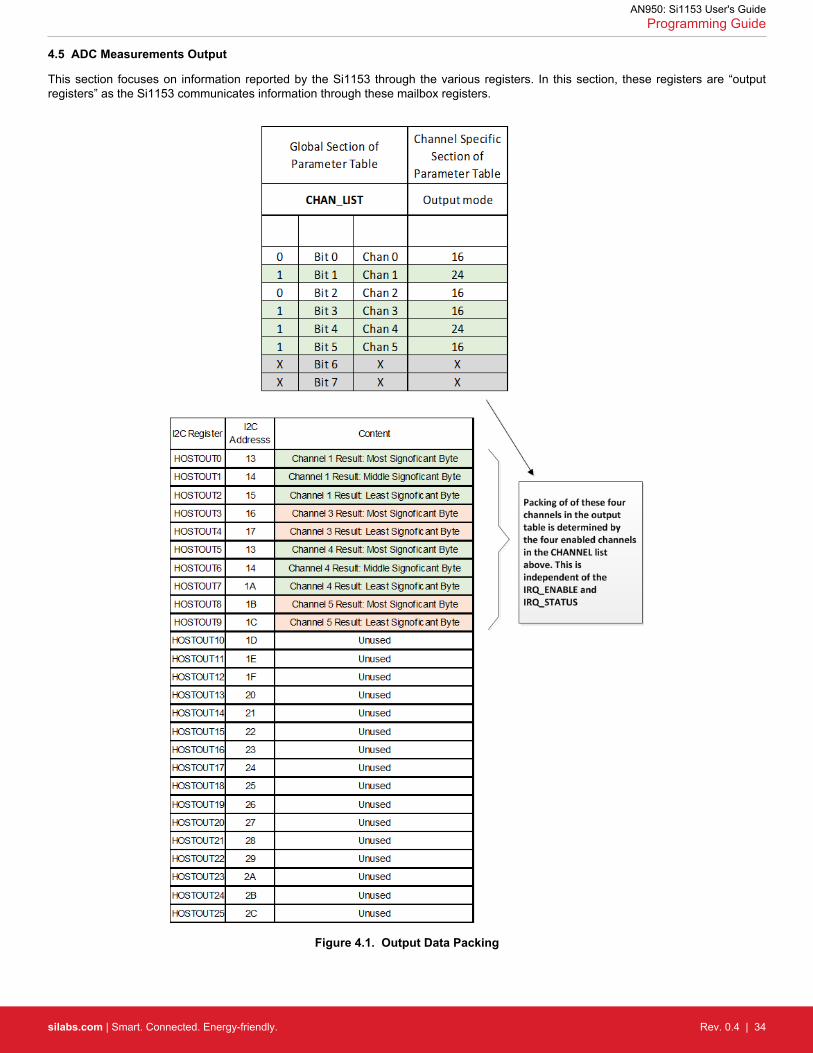
4.5 ADC Measurements Output
This section focuses on information reported by the Si1153 through the various registers. In this section, these registers are “outputregisters” as the Si1153 communicates information through these mailbox registers.
Figure 4.1. Output Data Packing
AN950: Si1153 User's GuideProgramming Guide
silabs.com | Smart. Connected. Energy-friendly. Rev. 0.4 | 34

4.5.1 Byte Alignment
The Si1153 has a total of 26 output registers. In all modes, the CHAN_LIST configuration determines how the data is stacked in the 26byte output field. It is done on a first-come first-served basis, with the enabled lower channels taking up the lower addresses.
The format of the output is either a 16-bit unsigned number or a 24-bit signed number, determined by the selection made in the channelsetup.
It is recommended that these output registers be read using an I2C Burst Read operation.
Register ordering is “big-endian”.
4.5.2 Host Interrupt Latency
When the Si1153 has started an autonomous measurement, the output registers are updated directly from the internal controller. Thehost interrupt handler is expected to read the I2C registers before the next measurement cycle begins. The choice of the measurementrate should take the interrupt latency into consideration.
If the host reads the output registers while the Si115x is updating them with the next measurement, it is possible that the host may readan upper byte from the previous measurement and a lower byte from the current measurement. For this reason, it is imperative that thehost reads the output before the next group of measurements is started.
In general, the host must read the registers any time after the interrupt pin has asserted up to the measurement time minus the maxi-mum measurement time. The host interrupt latency should allow the output registers to be read by this time frame. Refer to 5. Latencyfor more details on the latency of various measurement channel combinations.
4.5.3 ADC Number System
Due to effect of ambient noise, it is possible that the values provided by the Si1153 can be slightly negative. If the output format isconfigured as 16-bit unsigned mode, all negative values will be treated as 0. If the output format is configured as 24-bit unsigned mode,the negative value will be placed on the output registers as it is.
The Si1153 uses the ADC value, 0xFFFF, whenever the ADC saturates.
AN950: Si1153 User's GuideProgramming Guide
silabs.com | Smart. Connected. Energy-friendly. Rev. 0.4 | 35
5. Latency
In autonomous measurement mode, measurements are performed periodically based on MEASRATE and MEASCOUNT as applicable.When autonomous measurement mode is initiated, the wake-up timer and measurement rate counters begin to count down, and thefirst set of measurements is available at the end of that initial count and periodically afterwards. Upon each measurement, the result isplaced in the corresponding data register, and the interrupt is triggered. By definition, the latency is zero.
In forced measurement mode, a measurement is processed as soon as possible. In the simplest case, where forced mode is used forCH0 proximity or ambient light measurement only, with DECIM_RATE set to 0 (48.8 µs measurement time) by default, the latency isgiven by the following formula:
t = tprocess + 2 × (tadcstart + 48.8μs × 2HW_GAIN )The values for tprocess and tadcstart can be found in the electrical specifications of the data sheet.
In both autonomous and forced mode, measurements are performed in the order from CH0 to CH5 when enabled, and all the latenciesapply cumulatively.
Conflicts may arise in some cases:• A forced measurement is requested while an autonomous measurement is in progress.• An autonomous measurement internal request from the wake-up timer occurs while a forced measurement is in progress.
In the above cases, measurement requests are executed in the order they have been received, and additional delays will be encoun-tered. The worst-case latency can be calculated by adding all potential latencies based on expected measurements. Careful systemdesign can prevent or minimize cumulative delays (e.g., by forcing measurements only after stopping the autonomous-measurementloop) or when no autonomous measurement is expected (e.g., immediately after an interrupt signals the last autonomous measure-ment).
AN950: Si1153 User's GuideLatency
silabs.com | Smart. Connected. Energy-friendly. Rev. 0.4 | 36
6. Power Consumption
Power consumption calculation proceeds in discrete steps. Since the Si1153x is in standby mode most of the time, the following dutycycle calculations are necessary to evaluate the overall power consumption:
1. Calculate the duty cycle associated with ADC measurement.2. Calculate the duty cycle associated with controller processing.3. Calculate the duty cycle associated with the Si1153 being in standby, (i.e. the rest of the time).4. Calculate the LED duty cycle, and multiply by the LED current and driver current.
The complete current-consumption formula is given below:IDD = DC ADC × Isuspend + DCProcess × Iactive + DCSB × Isleep + DC LED × ILED
Where DCADC, DCProcess, DCLED and DCSB are the duty cycles of the ADC measurements, the controller processing overhead, theLED “on” time, and the Si1153 standby time, respectively.
Iactive, Isuspend, ILED and Isleep are the device active current, ADC suspend current, LED current and standby current respectively. Typi-cal and maximum standby currents and active currents can be found in the Si1153 datasheet. Typical LED currents are listed in theSi1153 data sheet.
If multiple channels are used, the duty cycle is increased in proportion, and an additional term must be added for each additional LEDwith its corresponding duty cycle, current, and driver current.
Measurement duty cycles are ratios of a given period of time, t, over the measurement cycle and thus take the form:
DC xx =tActive
Measurement Cycle
The measurement cycle is set by MEASRATE and MEASCOUNT globally, and COUNTER_INDEX for the corresponding channel.
6.1 ADC Measurement Duty Cycle
The duty cycle of the ADC measurement is affected by the number of channels, the ADC setup time, the ADC gain, and the measure-ment rate according to the following formula:
DC ADC =2 × (number of channels) × (tsetup + 48.8μs × 2HW_GAIN )
tMEASRATE
Typically, tsetup is about 48.8 µs.
Power consumption can be minimized by reducing the HW_GAIN.
6.2 Controller Processing Duty Cycle
The controller processing duty cycle is determined by the number of channels and the total internal processing time including the setuptime and post processing time:
DCProcess =number of channels × tprocess
tMEASRATE
The sum of processing time per measurement tprocess is about 155 µs.
6.3 Standby Duty Cycle
The standby duty cycle is inferred from all the other duty cycles, thus:DCSB = 1 − DC ADC − DCProcess
AN950: Si1153 User's GuidePower Consumption
silabs.com | Smart. Connected. Energy-friendly. Rev. 0.4 | 37

6.4 LED Power
On each proximity measurement, the LED current is on for 48.8 µs times the gain. Thus, for each proximity channel, the LED duty cycleis:
DC LED = 48.8μs × 2HW_GAIN
tMEASRATE
The LED driver requires internal mirroring, which requires current based on the LED current setting. Thus for each LED current setting,there is a corresponding internal power draw. The LED-related extra current draw is not proportional to the set LED drive current.
If multiple LEDs are on for any given proximity cycle (Si1153 only), all respective LED currents and LED drive currents must be sum-med.
AN950: Si1153 User's GuidePower Consumption
silabs.com | Smart. Connected. Energy-friendly. Rev. 0.4 | 38

7. Additional Resources
Si1153-AA00/AA09/AA9X Data Sheet
AN521: IRLED Selection Guide for Si114x Proximity Applications
AN522: Using the Si1141 for Touchless Lavatory Appliances
AN523: Overlay Considerations for the Si114x Sensor
AN580: Infrared Gesture Sensing
AN950: Si1153 User's GuideAdditional Resources
silabs.com | Smart. Connected. Energy-friendly. Rev. 0.4 | 39

http://www.silabs.com
Silicon Laboratories Inc.400 West Cesar ChavezAustin, TX 78701USA
Smart. Connected. Energy-Friendly.
Productswww.silabs.com/products
Qualitywww.silabs.com/quality
Support and Communitycommunity.silabs.com
DisclaimerSilicon Laboratories intends to provide customers with the latest, accurate, and in-depth documentation of all peripherals and modules available for system and software implementers using or intending to use the Silicon Laboratories products. Characterization data, available modules and peripherals, memory sizes and memory addresses refer to each specific device, and "Typical" parameters provided can and do vary in different applications. Application examples described herein are for illustrative purposes only. Silicon Laboratories reserves the right to make changes without further notice and limitation to product information, specifications, and descriptions herein, and does not give warranties as to the accuracy or completeness of the included information. Silicon Laboratories shall have no liability for the consequences of use of the information supplied herein. This document does not imply or express copyright licenses granted hereunder to design or fabricate any integrated circuits. The products are not designed or authorized to be used within any Life Support System without the specific written consent of Silicon Laboratories. A "Life Support System" is any product or system intended to support or sustain life and/or health, which, if it fails, can be reasonably expected to result in significant personal injury or death. Silicon Laboratories products are not designed or authorized for military applications. Silicon Laboratories products shall under no circumstances be used in weapons of mass destruction including (but not limited to) nuclear, biological or chemical weapons, or missiles capable of delivering such weapons.
Trademark InformationSilicon Laboratories Inc.® , Silicon Laboratories®, Silicon Labs®, SiLabs® and the Silicon Labs logo®, Bluegiga®, Bluegiga Logo®, Clockbuilder®, CMEMS®, DSPLL®, EFM®, EFM32®, EFR, Ember®, Energy Micro, Energy Micro logo and combinations thereof, "the world’s most energy friendly microcontrollers", Ember®, EZLink®, EZRadio®, EZRadioPRO®, Gecko®, ISOmodem®, Precision32®, ProSLIC®, Simplicity Studio®, SiPHY®, Telegesis, the Telegesis Logo®, USBXpress® and others are trademarks or registered trademarks of Silicon Laborato-ries Inc. ARM, CORTEX, Cortex-M3 and THUMB are trademarks or registered trademarks of ARM Holdings. Keil is a registered trademark of ARM Limited. All other products or brand names mentioned herein are trademarks of their respective holders.