Embed Size (px)
Citation preview
DOKUZ EYLÜL UNIVERSITY
GRADUATE SCHOOL OF NATURAL AND APPLIED SCIENCES
ANALOG CIRCUIT DESIGN USING CURRENT
AND TRANSRESISTANCE AMPLIFIERS
by
Selçuk KILINÇ
June, 2006
İZMİR
ANALOG CIRCUIT DESIGN USING CURRENT
AND TRANSRESISTANCE AMPLIFIERS
A Thesis Submitted to the
Graduate School of Natural and Applied Sciences of Dokuz Eylül University
In Partial Fulfillment of the Requirements for the Degree of Doctor of Philosophy in
Electrical and Electronics Engineering
by
Selçuk KILINÇ
June, 2006
İZMİR
Ph.D. THESIS EXAMINATION RESULT FORM
We have read this thesis entitled “ANALOG CIRCUIT DESIGN USING
CURRENT AND TRANSRESISTANCE AMPLIFIERS” completed by Selçuk
KILINÇ under supervision of Assoc. Prof. Dr. Uğur ÇAM and we certify that in
our opinion it is fully adequate, in scope and in quality, as a thesis for the degree of
Doctor of Philosophy.
Assoc. Prof. Dr. Uğur ÇAM
Supervisor
Prof. Dr. Haldun KARACA Prof. Dr. Erol UYAR
Committee Member Committee Member
Prof. Dr. Hakan KUNTMAN Prof. Dr. Cüneyt GÜZELİŞ
Jury Member Jury Member
Prof. Dr. Cahit HELVACI
Director Graduate School of Natural and Applied Sciences
ii

ACKNOWLEDGMENTS
I would like to thank my supervisor Assoc. Prof. Dr. Uğur ÇAM for his valuable
guidance and support during the course of this thesis. I wish to express my
appreciation to Prof. Dr. Hakan KUNTMAN and Prof. Dr. Haldun KARACA for
their useful comments. I am also grateful to the Scientific and Technical Research
Council of Turkey, Münir Birsel Foundation for providing financial support during
my Ph.D. studies. Finally, I sincerely thank my parents for their understanding and
never ending support throughout my life.
Selçuk KILINÇ
iii
ANALOG CIRCUIT DESIGN USING CURRENT
AND TRANSRESISTANCE AMPLIFIERS
ABSTRACT
Within the four amplifier types, voltage operational amplifier (op-amp) and
operational transconductance amplifier (OTA) have been widely utilized in analog
circuit design. On the other hand, the remaining two amplifiers, namely current
operational amplifier (COA) and operational transresistance amplifier (OTRA), have
not been received much attention until recently. However, the COA and OTRA have
some advantageous properties that can be enjoyed by analog circuits. Both of them
are characterized by internally grounded input terminals, leading to circuits that are
insensitive to the stray capacitances. This feature also yields eliminating response
limitations incurred by capacitive time constants. The output terminals of the COA
are characterized by high impedance while the OTRA exhibits low output
impedance. These make easy to drive loads without addition of a buffer for current
mode and voltage mode circuits, which use COA and OTRA, respectively. The
current differencing and internally grounded inputs of these elements make it
possible to implement the circuits with MOS-C realization. In this thesis, two CMOS
realizations for the COA are presented. They are basically obtained by cascading an
OTRA and a dual output OTA. Current mode first order allpass filters, biquadratic
filters and sinusoidal oscillators have been introduced as the applications of the
CMOS COAs. Some analog circuits employing the OTRA have also been presented.
Among these are first order allpass filters, all five different forms of second order
filters, multifunction biquads, transimpedance type biquadratic filters and sinusoidal
oscillators. OTRA based circuits for the realization of nth order voltage transfer
function and fully controllable negative inductance are also included. The
workability of the presented circuits has been verified by PSPICE simulation results.
Some of the circuits are also tested experimentally.
Keywords: analog circuit design, integrated circuits, current operational amplifiers,
operational transresistance amplifiers
iv
AKIM VE GEÇİŞ-DİRENÇ KUVVETLENDİRİCİLER KULLANARAK
ANALOG DEVRE TASARIMI
ÖZ
Dört kuvvetlendirici türü arasında, gerilim işlemsel kuvvetlendirici (op-amp) ve
işlemsel geçiş-iletkenlik kuvvetlendirici (OTA), analog devre tasarımında yaygın
olarak kullanılmaktadır. Diğer yandan, geriye kalan iki kuvvetlendirici, yani akım
işlemsel kuvvetlendirici (COA) ve işlemsel geçiş-direnç kuvvetlendirici (OTRA),
son zamanlara kadar fazla ilgi çekmemiştir. Bununla birlikte, COA ve OTRA, analog
devreler tarafından kullanılabilecek olan bazı avantajlı özelliklere sahiptir. Her ikisi
de içten topraklı giriş uçları ile karakterize edildiğinden kaçak kapasitelere duyarsız
devrelere yol açarlar. Aynı zamanda bu özellik, kapasitif zaman sabitleri nedeniyle
oluşan cevap sınırlamalarını yok eder. COA’nın çıkış uçları yüksek empedans olarak
karakterize edilmekte, OTRA ise alçak empedans çıkış ucu sergilemektedir. Bu
durum, COA kullanan akım modlu ve OTRA kullanan gerilim modlu devrelerde,
bağlanacak yüklerin tampon devresi eklenmeksizin sürülmesini kolaylaştırır. Bu
elemanların akım farkı alan ve içten topraklı olan girişleri, devrelerin MOS-C olarak
gerçeklenmesini mümkün kılar. Bu tezde, COA için iki CMOS gerçeklemesi
sunulmuştur. Bunlar temelde bir OTRA ile çift çıkışlı bir OTA’nın art arda
bağlanmasıyla elde edilmiştir. CMOS COA’ların uygulamaları olarak, akım modlu
birinci derece tüm geçiren filtreler, ikinci derece filtreler ve sinüsoidal osilatörler
tanıtılmıştır. OTRA kullanan bazı analog devreler de sunulmuştur. Bunlar arasında,
birinci derece tüm geçiren filtreler, bütün beş ayrı türdeki ikinci derece filtreler, çok
fonksiyonlu filtreler, geçiş-empedans tipindeki filtreler ve sinüsoidal osilatörler yer
almaktadır. Ayrıca, n. dereceden gerilim transfer fonksiyonu ve tümüyle kontrol
edilebilen negatif endüktans gerçeklemeleri için OTRA tabanlı devreler
içerilmektedir. Sunulan devrelerin çalışabilirliği, PSPICE benzetim sonuçlarıyla
gösterilmiştir. Devrelerin bazıları deneysel olarak da test edilmiştir.
Anahtar Kelimeler: analog devre tasarımı, tümdevreler, akım işlemsel
kuvvetlendirici, işlemsel geçiş-direnç kuvvetlendirici
v
CONTENTS
Page
THESIS EXAMINATION RESULT FORM……………………………………...…ii
ACKNOWLEDGEMENTS.………………………………………………......…..…iii
ABSTRACT.…………………………………………...………………………..…..iv
ÖZ……………………………………………………………………………….……v
CONTENTS………………………………………….……………………................vi
CHAPTER ONE – INTRODUCTION…………………………………………….1
1.1 Analog Circuit Design ............................................................................. 1
1.2 Integrated Circuit Technologies............................................................... 2
1.3 Current Mode Approach .......................................................................... 4
1.4 Current Mode Building Blocks ................................................................ 7
1.5 Current and Tranresistance Amplifiers .................................................... 9
1.6 Thesis Outline ........................................................................................ 11
CHAPTER TWO – CURRENT AND TRANSRESISTANCE AMPLIFIERS..12
2.1 Ideal Amplifier ....................................................................................... 12
2.2 Reciprocity and Adjoint Networks ........................................................ 13
2.3 Classification of Amplifiers ................................................................... 15
2.4 Closed Loop Amplifier Performance ..................................................... 18
2.5 Current Operational Amplifier............................................................... 20
2.6 Operational Transresistance Amplifier .................................................. 23
CHAPTER THREE – CMOS REALIZATION EXAMPLES FOR COA…..…26
3.1 Block Diagram Model of the COA ........................................................ 26
3.2 Implementation of COA Using Current Conveyors............................... 27
3.3 The First Example of CMOS COA Realization..................................... 31
3.4 The Second Example of CMOS COA Realization ................................ 35
vi
CHAPTER FOUR – ANALOG CIRCUIT DESIGN USING COA…………….39
4.1 Current Mode First Order Allpass Filters .............................................. 39
4.2 Current Mode Biquadratic Filters .......................................................... 45
4.3 Current Mode Sinusoidal Oscillators ..................................................... 54
CHAPTER FIVE – ANALOG CIRCUIT DESIGN USING OTRA.………..….60
5.1 Allpass and Notch Filters ....................................................................... 60
5.2 Lowpass, Highpass and Bandpass Biquads ........................................... 69
5.3 Realization of nth Order Voltage Transfer Function ............................. 72
5.4 Multifunction Biquads ........................................................................... 80
5.5 Transimpedance Type Fully Integrated Biquadratic Filters................... 84
5.6 Sinusoidal Oscillators............................................................................. 93
5.7 Realization of Fully Controllable Negative Inductance......................... 95
CHAPTER SIX – CONCLUSION………………………………………………106
6.1 Concluding Remarks............................................................................ 106
6.2 Future Work ......................................................................................... 107
REFERENCES……………………………………………………………………108
vii

CHAPTER ONE
INTRODUCTION
1.1 Analog Circuit Design
Analog circuit design is the successful implementation of analog circuits and
systems using integrated circuit (IC) technology. Analog circuits and systems have
an important role in the implementation and application of very large scale
integration (VLSI) technology. The development of VLSI technology, coupled with
the demand for more signal processing integrated on a single chip, has resulted in an
increased need for the design of effective analog ICs (Allen & Holberg, 1987).
Analog circuit design is becoming increasingly important with growing
opportunities. The emergence of ICs incorporating mixed analog and digital
functions on a single chip has led to an advanced level of analog design (Toumazou,
Lidjey & Haigh, 1990).
Since the early 1970’s, the field of analog circuits and systems has developed and
matured. During this period, much has been made of the competition between analog
and digital system design strategies. Advances in digital VLSI have enabled
memories, microprocessors, and digital signal processors (Laker & Sansen, 1994).
As the level of integration increased in IC technology, digital circuit implementation
became more desirable than analog circuit implementation. This is because of its
robustness, reliability, accuracy, ease of design, programmability, flexibility, and
cost (Toumazou et al., 1990). With the advances of VLSI technology, digital signal
processing is proliferating and penetrating into more and more applications. Many
applications which have been traditionally implemented in analog domain have been
moved to digital, such as digital audio and wireless cellular phones (Allen &
Holberg, 1987).
Even if digital circuits could always outperform analog circuits with smaller or
equivalent area, analog circuits would still be required (Toumazou et al., 1990).
There are some facts that make analog ICs and systems increasingly important. First
1
2
of all, the natural world is analog. Thus, analog systems are needed in information
acquisition systems in order to prepare analog information for conversion to digital
format (Laker & Sansen, 1994). In other words, interface functions are required
between the real world and the silicon system due to the fact that most of the signals
in the physical world are analog. The primary information acquired from the real
world is usually in the form of time continuous analog signals and must be interfaced
to digital circuitry. The result of the digital processing must likewise be converted to
back to analog form. In a digital signal processing system, amplification, filtering,
and signal conditioning are required before converting to the digital format. After
output signal digital to analog conversion, again filtering is needed. Finally, the
smoothed output signal must be amplified to the appropriate power level to achieve
the desired effect (Toumazou et al., 1990). That is, analog pre-processing before the
analog to digital conversion and post-processing after the digital to analog
conversion are needed for a digital signal processing system. Therefore, analog
circuits will continue to be a part of large VLSI digital systems (Allen & Holberg,
1987).
In recent years, the quest for ever smaller and cheaper electronic systems has led
manufacturers to integrate entire system onto a single chip. It is now becoming
common to find that a single mixed analog and digital (mixed mode) IC contains
both a digital signal processor and all the analog interface circuits required to interact
with its external analog transducers and sensors (Aaserud & Nielsen, 1995). That is,
analog and digital VLSI circuits coexist on the same chip (Laker & Sansen, 1994).
On the other hand, there remain many signal processing tasks that are best performed
by analog circuits. Complete analog systems will still continue to be required in
some applications, mainly those in which the frequency of operation is too high for
digital implementation or in very low power applications (Aaserud & Nielsen, 1995).
1.2 Integrated Circuit Technologies
The element of principal importance concerning analog signal processing is the
trend of technology. There are mainly four viable integrated technologies for analog
3
circuits. These technologies are bipolar, complementary metal oxide semiconductor
(CMOS), BiCMOS, and gallium arsenide (GaAs) (Toumazou et al., 1990). Much of
the analog design during the 1960’s and 1970’s was done in bipolar technology. The
1980’s was an era of rapid evolution of MOS analog ICs, in particular CMOS (Laker
& Sansen, 1994).
CMOS technology has become a dominant analog technology primarily because
of good quality capacitors, good switches and low power dissipation (Toumazou et
al., 1990). It provides very large scale integration of both high density digital circuits
and analog circuits for low cost. On the other hand, comparison between the bipolar
and CMOS technologies in terms of bandwidth and noise favors the bipolar from an
analog viewpoint. However, a similar comparison made from a digital viewpoint
would come up on the side of CMOS. Therefore, since large volume technology will
be driven by digital demands, CMOS is an obvious result as the technology of
availability. Furthermore, the potential for technology improvement for CMOS is
greater than for bipolar and the performance in CMOS generally increases with
decreasing channel length (Allen & Holberg, 1987).
During the 1990’s, we have seen the BiCMOS technology emerge as a serious
contender to the original technologies (Laker & Sansen, 1994). BiCMOS technology
combines both bipolar and CMOS technologies and obviously has the advantages of
both. BiCMOS offers the ability of low power dissipation using CMOS and high
speed performance using bipolar (Toumazou et al., 1990). On the other hand, it is
somewhat more expensive to fabricate. GaAs technology is quickly maturing and
offers many possibilities as a niche technology. From an analog viewpoint, GaAs is
well developed for microwave analog but less developed for analog signal processing
(Toumazou et al., 1990).
It is clear that CMOS technology is preferred for digital design. Since analog and
digital functions are placed onto a single chip in modern VLSI systems, the use of
CMOS technology for analog circuits is also preferred. CMOS process
implementation is preferable because CMOS process makes it possible to implement
4
mixed signal circuit chips with lower cost (Takagi, 2001). During the past years, we
have seen a proliferation of mixed analog/digital VLSI ICs realized in state of the art
CMOS technologies to optimize cost and power dissipation in consumer products,
many of which are pocket size and battery powered (Laker & Sansen, 1994). It has
also the advantages of low power consumption and high integration density.
Therefore, dominant VLSI technology for analog circuits is CMOS up to GHz range.
1.3 Current Mode Approach
Analog processing systems traditionally use input and output voltages which are
in charge of carrying the information. The voltage – current duality, which results
from the Kirchoff’s laws, as well as from the Thevenin’s and Norton’s theorems,
allows analog circuits working from current signals to be obtained, too. Because the
measurement of a voltage across an impedance was easier than the measurement of
the current flowing through this impedance, engineers used to work with voltages
rather than with currents (Fabre, 1995a). Thus, it has become customary in electrical
engineering to think of signal processing in terms of voltage variables rather than
current variables. This tendency has resulted in voltage signal processing circuits
such as voltage amplifiers, voltage integrators, filters which realize a voltage transfer
function, etc (Allen & Terry, 1980).
Most analog signal processing is accomplished through the use of feedback
around a high gain voltage amplifier to achieve a well defined voltage transfer
function which is independent of the active devices. The high gain voltage amplifier
may consist of discrete components or may be an IC such as a voltage operational
amplifier (op-amp). This approach has worked well as evidenced by a large number
of analog circuits which use the voltage op-amp (Allen & Terry, 1980).
Since the introduction of ICs, the op-amp has served as the basic building block in
analog circuit design and has been widely used in a variety of applications such as
addition/subtraction circuits, amplifiers, multipliers/dividers, interface circuitry,
digital to analog converters, analog to digital converters, variable gain amplifiers,
5
filters, oscillators, etc (Koli, 2000). Most of the systems based on voltage op-amps
represent the signal of interest in the voltage domain (Youssef & Soliman, 2005).
High frequency operation is an ever present demand on analog circuits. Analog
circuits are always requested to work at high frequencies where digital signal
processing faces difficulties with implementation. In addition to this demand, a
recent advanced fabrication process forces analog circuits to operate under supply
voltages as low as possible. This is because of reduction in tolerant voltages of
transistors, reduction in power consumption, the same chip implementation together
with digital circuits, etc (Takagi, 2001). In these respects, realization of low voltage
and high frequency analog circuits is one of the most attractive and important issues
in many signal processing fields.
However, the classical op-amp suffers from limited gain-bandwidth product
problems and from low slew rate at its output. Many circuits employing op-amps
have been designed and described. The limited gain-bandwidth product of the op-
amp affects the parameters of the circuits designed. They remain, therefore,
unsatisfactory at higher frequencies (Budak, 1974).
In order to correspond to the severe demands for high frequency and low power
supply voltage operation on analog circuits, designers made plenty of attempts.
Among these is the current mode approach. There has been a great shift in analog
circuit design towards representing signals with current instead of voltage to achieve
high performance analog circuits in CMOS technology. So, in the past years current
mode circuits began to receive a great attention as a new alternative to voltage mode
circuits. This is because one of the most promising solutions to high frequency and
low voltage operation is thought to be current signal processing (Takagi, 2001). A
current mode circuit may be taken to mean any circuit in which current is used as the
active variable in preference to voltage, either throughout the whole circuit or only in
certain critical areas (Wilson, 1990).
6
Current mode circuits have been receiving considerable attention due to their
potential advantages such as inherently wide bandwidth, higher slew rate, wider
dynamic range, simpler circuitry, low voltage operation and low power consumption
(Toumazou et al., 1990). Furthermore, current mode circuits are suitable for
integration with CMOS technology and thus have become more and more attractive
in electronic circuit design in recent years (Toker, Kuntman, Çiçekoğlu & Dişçigil,
2002).
Transistors are more suitable for processing currents rather than voltages because
they are inherently current mode i.e., both bipolar and MOS transistors are current
output devices. An important number of elementary mathematical functions can be
obtained easier from current signals rather than from voltage. In this order, to
generate the sum of various currents flowing to ground does not necessitate to use
any passive components. This can easily be obtained onto any virtually grounded
node. On the contrary, summing several voltages is not as easy. The later needs
several resistances to achieve respectively both voltage-current conversion on input
and current-voltage conversion on output. The operation of summation being also
obtained as before, from current signals (Fabre, 1995a). Therefore, mathematical
operations of adding, subtracting or multiplying signals represented by currents are
simpler to perform than when they are represented by voltages. For this reason,
integrated current mode system realizations are closer to the transistor level than the
conventional voltage mode realizations and therefore simpler circuits and systems
should result (Koli, 2000).
In voltage mode circuits the high valued resistors with parasitic capacitances
create a dominant pole at a relative low frequency, which limits the bandwidth. In
general, the node impedances in current mode circuits are low and the voltage swings
are small. Thus the time constant is reduced and also the time required for charging
and discharging a parasitic capacitor is kept small. Hence the slew rate for current
mode circuits will be sufficiently high. They are well suited to work at higher
frequencies and thus are often used in communication circuits (Toker et al., 2002).
7
The low supply voltage operation is achieved because small voltages appear on the
nodes.
From these major merits many analog circuit designers believe that current mode
circuit techniques meet the severe demands for low power supply voltage and high
frequency operation on analog circuits. Although a current mode approach is
promising, voltage mode circuits have a lot of merits against current mode circuits.
First of all, a fact that there exist plenty of practically used circuits is very important
in terms of reliability. Because of this, most of the systems use not current signals but
voltage signals. Therefore, a voltage mode approach is still attractive even though a
current mode one becomes popular (Takagi, 2001).
1.4 Current Mode Building Blocks
To overcome the certain limitations of op-amp in analog circuits, many new
building blocks that are suitable for current mode circuits have been introduced.
Among these current conveyors are very famous.
The concept of the current conveyor was first presented in 1968 (Smith & Sedra,
1968) and further developed to a second generation current conveyor in 1970 (Sedra
& Smith, 1970). The current conveyor is intended as a general building block as with
the op-amp. On the other hand, neither of these building blocks became popular as a
consequence of the introduction of the integrated op-amp at the time. Because of the
op-amp concept has been current since the late 1940’s, it is difficult to get any other
similar concept widely accepted. Additionally, integrated current conveyors were
difficult to realize due to the lack of high performance integration technologies in the
1970’s. During the 1980’s, research societies started to notice that the voltage op-
amp is not necessarily the best solution to all analog circuit design problems. Voltage
op-amps do not perform well in applications where a current output signal is needed
and consequently there is an application field for current conveyor circuits. Since
current conveyors operate without any global feedback, a different high frequency
behavior compared to op-amp circuits results (Koli, 2000).
8
In many applications, only one of the virtual grounds in the input terminals of the
first generation current conveyor is used and the unused terminal must be grounded
or otherwise connected to a suitable potential. This grounding must be done carefully
since a poorly grounded input terminal may cause an unwanted negative impedance
at the other input terminal. Moreover, for many applications a high impedance input
terminal is preferable. For these reasons, the second generation current conveyor was
developed. It has one high and one low impedance input rather than the two low
impedance inputs of the first generation current conveyor. Yet another current
conveyor was proposed in 1995 (Fabre, 1995b). The operation of the third generation
current conveyor is similar to that of the first generation current conveyor, with the
exception that the currents in the input terminals flow in opposite directions. This
current conveyor can be used as an active current probe (Koli, 2000).
Furthermore, a commercial product, the current feedback operational amplifier,
became available. The high slew rate and wide bandwidth of this amplifier resulted
in its popularity in video amplifier applications. It provides the advantage of having
constant bandwidth irrespective of the gain as oppose to classical op-amp. It is also
used in voltage mode operation as well as in current mode. The current feedback
operational amplifier is in effect a positive second generation current conveyor with
an additional voltage buffer at the conveyor current output. The current at the
inverting input of the current feedback operational amplifier is transferred to the high
impedance current conveyor output, causing a large change in output voltage (Koli,
2000).
There are some other additional types of building blocks as the variations of the
current conveyors such as; differential voltage current conveyor, differential
difference current conveyor, controlled current conveyor, inverting current conveyor,
operational floating conveyor, current differencing buffered amplifier (CDBA), etc.
Most of these elements are unity gain amplifiers. There are many applications of
these building blocks both in voltage mode and current mode operation.
9
1.5 Current and Transresistance Amplifiers
In general, amplifiers are classified into four groups as voltage op-amp, current
operational amplifier (COA), operational transconductance amplifier (OTA) and
operational transresistance amplifier (OTRA). The voltage op-amp and the OTA
have been widely used in several applications for many years, whereas the COA and
the OTRA have not gained much attention until recently. The four devices can be
arranged into two dual pairs according to adjoint networks principle (Bordewijk,
1956; Tellegen, 1952). The voltage op-amp and the COA form one pair, while the
OTA and the OTRA constitute the other pair (Payne & Toumazou, 1996).
One of the most popular methods for transformation between the current domain
and the voltage domain in analog signal processing is the principle of adjoint
networks. Using this principle, any voltage mode circuit based on the op-amp can be
transformed to a current mode circuit using the COA (Bruun, 1994). The same
transformation is possible between the circuits that employ the OTA and the OTRA.
The COA is basically a differential current-controlled current source with a very
high, ideally infinite, current gain. It exhibits very low, ideally zero, input resistances
and very high, ideally infinite, output resistances.
As mentioned before, the COA is the current mode counterpart of the
conventional voltage op-amp and it is particularly suitable in transforming op-amp
based voltage mode circuits into their current mode equivalents. Since the voltage
op-amp has been used in wide range of applications operating in voltage mode for a
long time, its current mode counterpart, COA, seems to be the suitable candidate as
the active element of current mode circuits. Applying the adjoint networks theorem
to traditional designs based on voltage op-amps such as; amplifiers, integrators,
filters, etc. will result in current mode circuits performing the same function but
based on the COA.
10
Many of these current mode circuits can also be implemented using current
conveyors as the basic active building block. However, since the current conveyors
are unity gain elements, the transfer functions of the circuits are sensitive to the
current tracking errors of the current conveyors. It is a well known fact that open
loop circuits are less accurate compared to their high gain counterparts. On the other
hand, the COA is a high gain current-input, current-output device. Using this device
in negative feedback configuration makes it possible to obtain very accurate transfer
functions, essentially independent of its inaccurate open loop gain (Mucha, 1995).
Therefore, the COA seems to be the true current mode active element for current
mode circuits.
The applications of the COA include the implementation of instrumentation
amplifier (Yen & Gray, 1982), current comparator with hysteresis (Laopoulos,
Siskos, Bafleur, Givelin & Tornier, 1995), gyrator (Mucha, 1995), differential
switched current filter (Cheng & Wang, 1998; Zele, Allstot & Fiez, 1991), and
variable gain amplifiers (Youssef & Soliman, 2005). The COA is also used in
biomedical, industrial and aerospace applications (Wang, 1990). In addition, it is
particularly suitable for temperature sensors, photo sensors and, in general, whenever
the input source and/or the output are current signals (Kauert, Budde &. Kalz, 1995;
Van den Broeke & Nieuwkerk, 1993; Vanisri & Toumazou, 1992). A current
amplifier can be also arranged in a true multi-output fashion, since several current
output stages can be embedded. Finally, an interesting and almost unique property of
current amplifiers is their feasibility for nonlinear resistances in the feedback
network, thanks to the fact that the voltage drop across them is the same (Magram &
Arbel, 1994; Palmisano, Palumbo & Pennisi, 2000).
The OTRA is basically a differential current-controlled voltage source with a very
high, ideally infinite, transresistance gain. It exhibits very low, ideally zero, input and
output resistances.
The OTRA is also known as current differencing amplifier or Norton amplifier. It
was used in some applications, including filter realizations, in the late 1970’s and the
11
early 1980’s (Anday, 1977a; Anday, 1977b; Anday, 1982; Brodie, 1978). Although
the OTRA is commercially available from several manufacturers, it has not gained
much attention until recently. These commercial realizations have certain drawbacks.
On the other hand, in recent years, several high performance CMOS OTRA
realizations have been presented in the literature (J. J. Chen, Tsao & C. C. Chen,
1992; Salama & Soliman, 1999a). This leads to growing interest for the design of
OTRA based analog signal processing circuits. The OTRA has been used in the
realization of filters (Salama & Soliman, 1999a), oscillators (Çam, 2002; Salama &
Soliman, 2000), and variable gain amplifiers (Elwan, Soliman & Ismail, 2001).
1.6 Thesis Outline
The main objective of this thesis is to introduce new analog circuits using the
COA and OTRA. Chapter 2 presents the classification of amplifiers and gives the
properties of COA and OTRA. Block diagram representations and CMOS
realizations of the COA are given in Chapter 3. Current mode first order allpass
filters, biquadratic filters and sinusoidal oscillators that are all employ a single COA
as the active element are included in Chapter 4. Chapter 5 presents many new OTRA
based circuits including allpass and notch filters; lowpass, highpass and bandpass
biquads; high order filters; transimpedance type filters; sinusoidal oscillators and
negative inductance simulators. Concluding remarks are given in Chapter 6.
CHAPTER TWO
CURRENT AND TRANSRESISTANCE AMPLIFIERS
2.1 Ideal Amplifier
In 1954, Tellegen introduced the concept of an “ideal element” or “ideal
amplifier” (Tellegen, 1954) as a general building block for the implementation of
linear and nonlinear analog systems. This ideal device was a two-port with four
associated variables – V1, I1 at the input port and V2, I2 at the output port. When
represented geometrically in 4-D space the device could be defined by the planes
V1 = 0, I1 = 0 and V2, I2 arbitrary. The amplifier would therefore exhibit an infinite
power gain between the input and output ports (Payne & Toumazou, 1996).
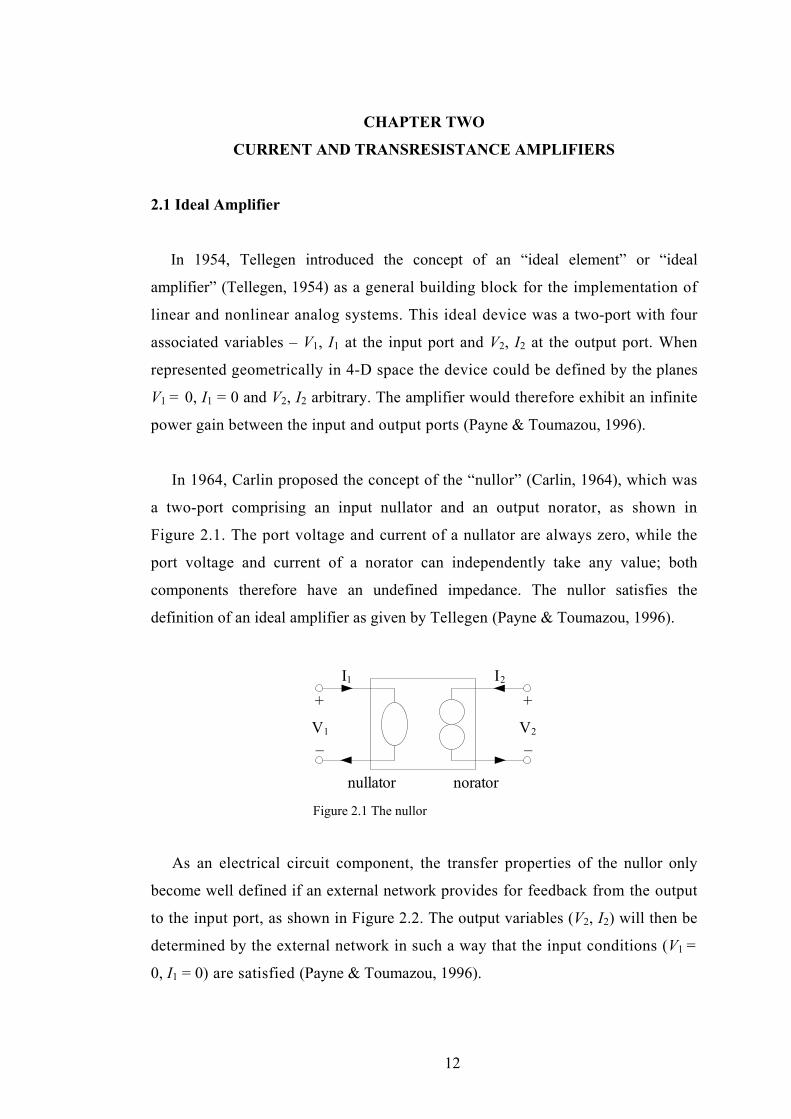
In 1964, Carlin proposed the concept of the “nullor” (Carlin, 1964), which was
a two-port comprising an input nullator and an output norator, as shown in
Figure 2.1. The port voltage and current of a nullator are always zero, while the
port voltage and current of a norator can independently take any value; both
components therefore have an undefined impedance. The nullor satisfies the
definition of an ideal amplifier as given by Tellegen (Payne & Toumazou, 1996).
I1 I2
V1
+
_V2
+
_
nullator norator Figure 2.1 The nullor
As an electrical circuit component, the transfer properties of the nullor only
become well defined if an external network provides for feedback from the output
to the input port, as shown in Figure 2.2. The output variables (V2, I2) will then be
determined by the external network in such a way that the input conditions (V1 =
0, I1 = 0) are satisfied (Payne & Toumazou, 1996).
12
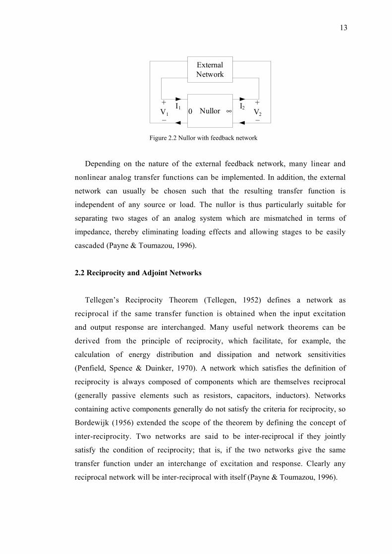
13
Nullor
ExternalNetwork
0 ∞I2 V2
+
_I1V1
+
_
Figure 2.2 Nullor with feedback network
Depending on the nature of the external feedback network, many linear and
nonlinear analog transfer functions can be implemented. In addition, the external
network can usually be chosen such that the resulting transfer function is
independent of any source or load. The nullor is thus particularly suitable for
separating two stages of an analog system which are mismatched in terms of
impedance, thereby eliminating loading effects and allowing stages to be easily
cascaded (Payne & Toumazou, 1996).
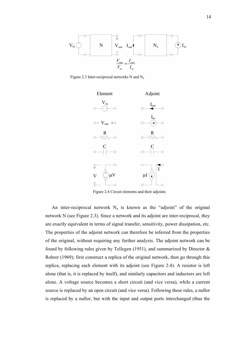
2.2 Reciprocity and Adjoint Networks
Tellegen’s Reciprocity Theorem (Tellegen, 1952) defines a network as
reciprocal if the same transfer function is obtained when the input excitation
and output response are interchanged. Many useful network theorems can be
derived from the principle of reciprocity, which facilitate, for example, the
calculation of energy distribution and dissipation and network sensitivities
(Penfield, Spence & Duinker, 1970). A network which satisfies the definition of
reciprocity is always composed of components which are themselves reciprocal
(generally passive elements such as resistors, capacitors, inductors). Networks
containing active components generally do not satisfy the criteria for reciprocity, so
Bordewijk (1956) extended the scope of the theorem by defining the concept of
inter-reciprocity. Two networks are said to be inter-reciprocal if they jointly
satisfy the condition of reciprocity; that is, if the two networks give the same
transfer function under an interchange of excitation and response. Clearly any
reciprocal network will be inter-reciprocal with itself (Payne & Toumazou, 1996).
14
Vin Vout
+
_N IinNaIout
in
out
in
out
II
VV =
Figure 2.3 Inter-reciprocal networks N and Na
Vin
Element Adjoint
Iout
Vout +_Iin
R R
C C
µV+_V
+
_
IµI
Figure 2.4 Circuit elements and their adjoints
An inter-reciprocal network Na is known as the “adjoint” of the original
network N (see Figure 2.3). Since a network and its adjoint are inter-reciprocal, they
are exactly equivalent in terms of signal transfer, sensitivity, power dissipation, etc.
The properties of the adjoint network can therefore be inferred from the properties
of the original, without requiring any further analysis. The adjoint network can be
found by following rules given by Tellegen (1951), and summarized by Director &
Rohrer (1969); first construct a replica of the original network, then go through this
replica, replacing each element with its adjoint (see Figure 2.4). A resistor is left
alone (that is, it is replaced by itself), and similarly capacitors and inductors are left
alone. A voltage source becomes a short circuit (and vice versa), while a current
source is replaced by an open circuit (and vice versa). Following these rules, a nullor
is replaced by a nullor, but with the input and output ports interchanged (thus the
15
nullor is “self inter-reciprocal” or “self adjoint”). Adjoint networks are also known
as “dual” networks, since they are equivalent under an interchange of voltage and
current signals. Figure 2.5 illustrates the adjoint network principle (Payne &
Toumazou, 1996).
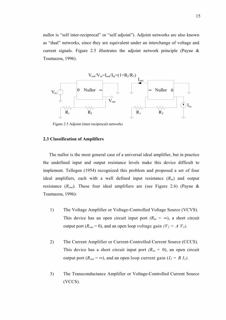
Nullor0 ∞
Iin
R1 R2
Vin
Vout
Nullor
R1 R2
0∞
Iout
Vout/Vin=Iout/Iin=(1+R2/R1)
Figure 2.5 Adjoint (inter-reciprocal) networks
2.3 Classification of Amplifiers
The nullor is the most general case of a universal ideal amplifier, but in practice
the undefined input and output resistance levels make this device difficult to
implement. Tellegen (1954) recognized this problem and proposed a set of four
ideal amplifiers, each with a well defined input resistance (Rin) and output
resistance (Rout). These four ideal amplifiers are (see Figure 2.6) (Payne &
Toumazou, 1996):
1) The Voltage Amplifier or Voltage-Controlled Voltage Source (VCVS).
This device has an open circuit input port (Rin = ∞), a short circuit
output port (Rout = 0), and an open loop voltage gain (V2 = A V1).
2) The Current Amplifier or Current-Controlled Current Source (CCCS).
This device has a short circuit input port (Rin = 0), an open circuit
output port (Rout = ∞), and an open loop current gain (I2 = B I1).
3) The Transconductance Amplifier or Voltage-Controlled Current Source
(VCCS).
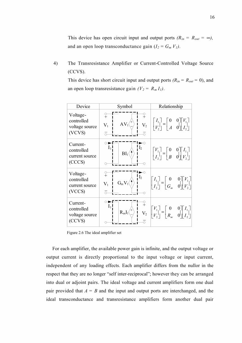
16
This device has open circuit input and output ports (Rin = Rout = ∞),
and an open loop transconductance gain (I2 = Gm V1).
4) The Transresistance Amplifier or Current-Controlled Voltage Source
(CCVS).
This device has short circuit input and output ports (Rin = Rout = 0), and
an open loop transresistance gain (V2 = Rm I1).
BI1
GmV1V1
+
_
RmI1+_ V2
+
_
AV1+_V1
+
_V2
+
_
Voltage-controlled voltage source (VCVS)
Device Symbol Relationship
Current-controlled current source (CCCS)
Voltage-controlled current source (VCCS)
Current-controlled voltage source (CCVS)
=
2
1
2
1
000
IV
AVI
=
2
1
2
1
000
VI
BIV
=
2
1
2
1
000
VV
GII
m
=
2
1
2
1
000
II
RVV
m
I1
I1 I2
I2
Figure 2.6 The ideal amplifier set
For each amplifier, the available power gain is infinite, and the output voltage or
output current is directly proportional to the input voltage or input current,
independent of any loading effects. Each amplifier differs from the nullor in the
respect that they are no longer “self inter-reciprocal”; however they can be arranged
into dual or adjoint pairs. The ideal voltage and current amplifiers form one dual
pair provided that A = B and the input and output ports are interchanged, and the
ideal transconductance and transresistance amplifiers form another dual pair
17
provided that Gm = Rm, and the input and output ports are interchanged (Payne &
Toumazou, 1996).
The amplification of signals is perhaps the most fundamental operation in analog
signal processing, and in the early days amplifier circuit topologies were generally
optimized for specific applications. However the desirability of a general purpose
high gain analog amplifier was recognized by system designers and IC
manufacturers alike, since the application of negative feedback allows many analog
circuit functions (or “operations”) to be implemented accurately and simply. A
general purpose device would also bring economies of scale, reducing the price and
allowing ICs to be used in situations where they may have previously been avoided
on the basis of cost. “Operational amplifiers” (op-amps) were thus featured among
the first generation of commercially available ICs (Payne & Toumazou, 1996).
Of the four amplifier types described by Tellegen, the voltage op-amp (VCVS)
has emerged as the dominant architecture almost to the exclusion of all others, and
this situation has a partly historical explanation. Early high gain amplifiers were
implemented using discrete thermionic valves which were inherently voltage-
controlled devices, and a controlled voltage output allowed stages to be easily
cascaded. The resulting voltage op-amp architectures were translated to silicon with
the development of IC technologies, and the device has since become ubiquitous to
the area of analog signal processing. The architecture of the voltage op-amp has
several attractive features; for example, the differential pair input stage is very good
at rejecting common mode signals. In addition a voltage op-amp only requires a
single ended output to simultaneously provide negative feedback and drive a load,
and the implementation of a single ended output stage is a much simpler task than
the design of a fully differential or balanced output (Payne & Toumazou, 1996).
On the negative side, the architecture of the voltage op-amp produces certain
inherent limitations in both performance and versatility. The performance of the
voltage op-amp is typically limited by a fixed gain-bandwidth product and a slew
rate whose maximum value is determined by the input stage bias current. The
18
versatility of the voltage op-amp is constrained by the single ended output, since the
device cannot be easily configured in closed loop to provide a controlled output
current (this feature requires the provision of a differential current output). The
voltage op-amp is therefore primarily intended for the implementation of closed
loop voltage processing (or “voltage mode”) circuits, and as a result most analog
circuits and systems have been predominantly voltage driven. Since it is often
desirable to maximize signal swings while minimizing the total power consumption,
voltage mode circuits generally contain many high impedance nodes to minimize
the total current consumption (Payne & Toumazou, 1996).
2.4 Closed Loop Amplifier Performance
The differing levels of input and output resistance among the various
amplifier types suggests that each might perform differently when presented with the
same external network. To investigate this further we return to Tellegen’s ideal
amplifier set (VCVS, CCCS, VCCS, CCVS), and derive the transfer functions
obtained when each amplifier is configured in turn to implement the various closed
loop functions shown in Figure 2.7 (Payne & Toumazou, 1996).
These circuits are chosen for the varying combinations of input source and
output drive which they impose on the ideal amplifier. The transfer functions for
these circuits are obtained by replacing the ideal amplifier by each of the specific
types (Payne & Toumazou, 1996).
There are four possible types of closed loop amplifiers which differ in the
combinations of input source an output drive as voltage to voltage (V-V) amplifier,
current to current (I-I) amplifier, current to voltage (I-V) amplifier, and voltage to
current (V-I) amplifier. The closed loop configurations for each kind of amplifier are
illustrated in Figure 2.7, where the symbol of the ideal amplifier was used. Table 2.1
summarizes the transfer functions which result for each kind of feedback amplifier
(Palmisano, Palumbo & Pennisi, 1999).

19
IdealAmp
+
_+
_
R1 R2
Vin
RS RL
Vout
IdealAmp
+
_+
_
R2
R1Iin RS
RLIout
IdealAmp
+
_+
_R2
RLIin RS
IdealAmp
+
_+
_R1
Vin
RS
Vout
RLIout
V-to-V amplifier I-to-I amplifier
I-to-V amplifier V-to-I amplifier Figure 2.7 Closed loop amplifier applications
Table 2.1 Transfer functions of amplifiers in Figure 2.7
V-V amplifier I-I amplifier I-V amplifier V-I amplifier
1+R2/R1 1+R2/R1 R2 1/R1
It can be observed that transfer functions in Table 2.1 only depend on the values
R1 and/or R2 regardless of the source and load resistances. This is a desirable feature
which closely approximates the performance of an ideal amplifier, since it reduces
interaction between cascaded active circuits and improves control over the loop gain
frequency response (module and phase). This feature greatly simplifies design from
the system to circuit point of view (Palmisano et al., 1999).
At this point one may conclude that any of the four amplifiers might alternatively
be used to implement the four types of feedback amplifiers. However, this is not the
case if we consider non-ideal amplifiers with finite (albeit large) open lop gain, even
20
with ideal internal resistances. In fact, under these assumptions, most of the 16
closed loop configurations, obtained by replacing the ideal amplifier with one of the
four specified amplifiers (voltage op-amp, COA, OTA, OTRA), will exhibit a loop
gain which is dependent on the source and/or load resistances (Palmisano et al.,
1999).
Since the closed loop gain and bandwidth are strictly related to the loop gain, they
will also depend on the source and/or load resistances. More specifically, this
detrimental condition characterizes all the configurations in which the op-amp is a
different type to the feedback amplifier (Palmisano et al., 1999).
To conclude, we can say that the best performance is obtained by following
“natural laws” and that the use of voltage op-amp is not the prime choice in
implementing current mode transfer functions. This perhaps represents the principal
motivation that leads researchers to design more appropriate op-amp architectures
which could be profitably used in current mode signal processing (Palmisano et al.,
1999).
2.5 Current Operational Amplifier
The circuit symbol of the COA is shown in Figure 2.8. The COA is a current-
controlled current source whose defining equation can be given as
zw
npz
n
p
II
IIBIV
V
=
−==
=
)(0
0
(2.1)
where B is the open loop current gain and ideally approaches infinity.
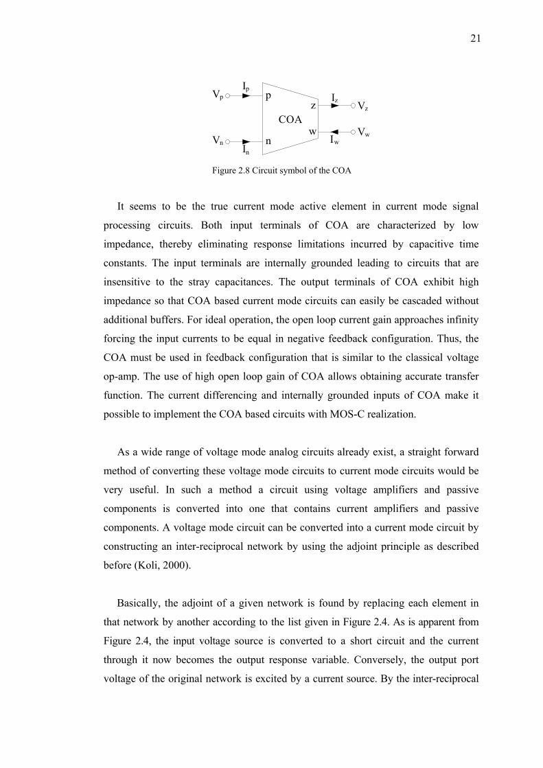
21
Ip
In
Vp
Vn
COA
p
n
z
w
Vz
Vw
Iz
Iw
Figure 2.8 Circuit symbol of the COA
It seems to be the true current mode active element in current mode signal
processing circuits. Both input terminals of COA are characterized by low
impedance, thereby eliminating response limitations incurred by capacitive time
constants. The input terminals are internally grounded leading to circuits that are
insensitive to the stray capacitances. The output terminals of COA exhibit high
impedance so that COA based current mode circuits can easily be cascaded without
additional buffers. For ideal operation, the open loop current gain approaches infinity
forcing the input currents to be equal in negative feedback configuration. Thus, the
COA must be used in feedback configuration that is similar to the classical voltage
op-amp. The use of high open loop gain of COA allows obtaining accurate transfer
function. The current differencing and internally grounded inputs of COA make it
possible to implement the COA based circuits with MOS-C realization.
As a wide range of voltage mode analog circuits already exist, a straight forward
method of converting these voltage mode circuits to current mode circuits would be
very useful. In such a method a circuit using voltage amplifiers and passive
components is converted into one that contains current amplifiers and passive
components. A voltage mode circuit can be converted into a current mode circuit by
constructing an inter-reciprocal network by using the adjoint principle as described
before (Koli, 2000).
Basically, the adjoint of a given network is found by replacing each element in
that network by another according to the list given in Figure 2.4. As is apparent from
Figure 2.4, the input voltage source is converted to a short circuit and the current
through it now becomes the output response variable. Conversely, the output port
voltage of the original network is excited by a current source. By the inter-reciprocal
22
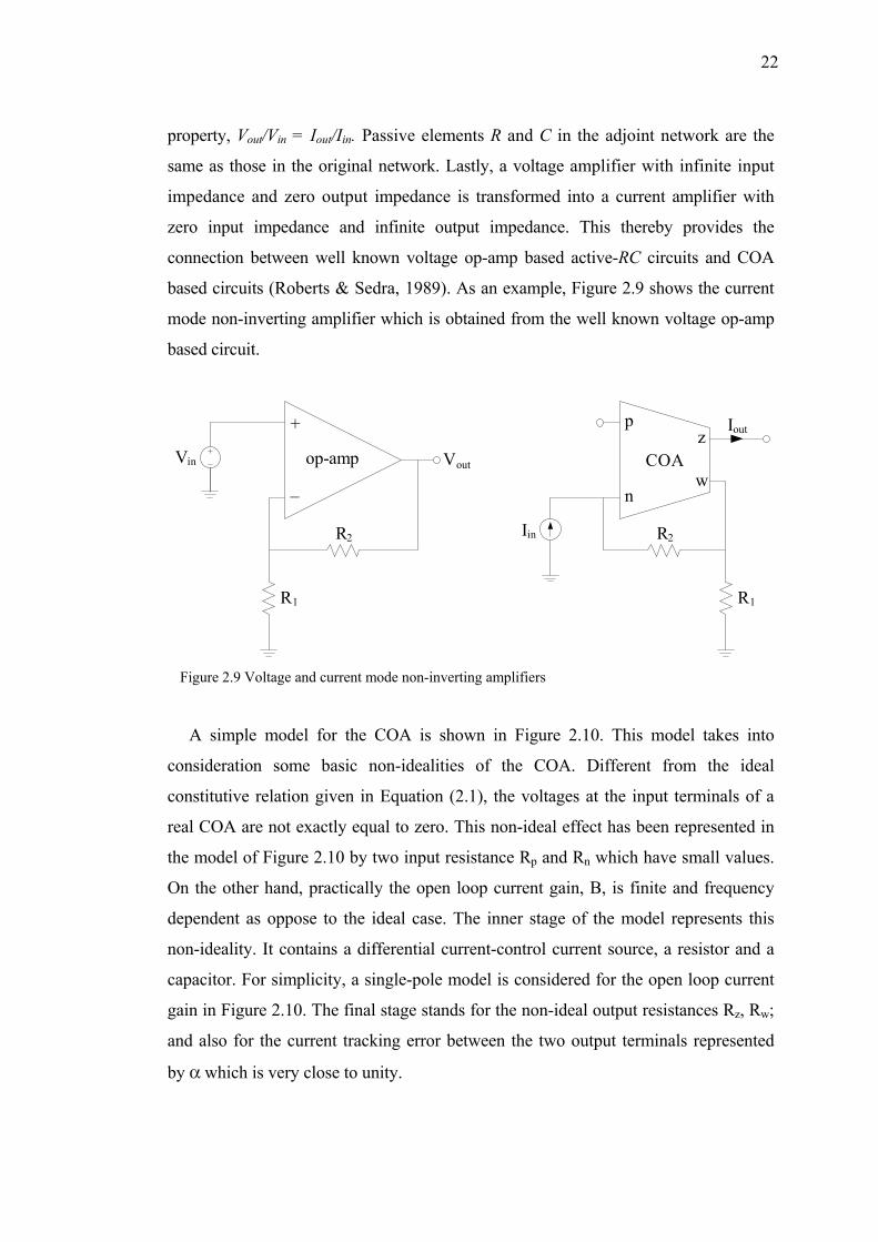
property, Vout/Vin = Iout/Iin. Passive elements R and C in the adjoint network are the
same as those in the original network. Lastly, a voltage amplifier with infinite input
impedance and zero output impedance is transformed into a current amplifier with
zero input impedance and infinite output impedance. This thereby provides the
connection between well known voltage op-amp based active-RC circuits and COA
based circuits (Roberts & Sedra, 1989). As an example, Figure 2.9 shows the current
mode non-inverting amplifier which is obtained from the well known voltage op-amp
based circuit.
COA
p
n
z
w
Iout
R2
R1
Iin
op-amp
+
_
Vin
R2
R1
Vout
Figure 2.9 Voltage and current mode non-inverting amplifiers
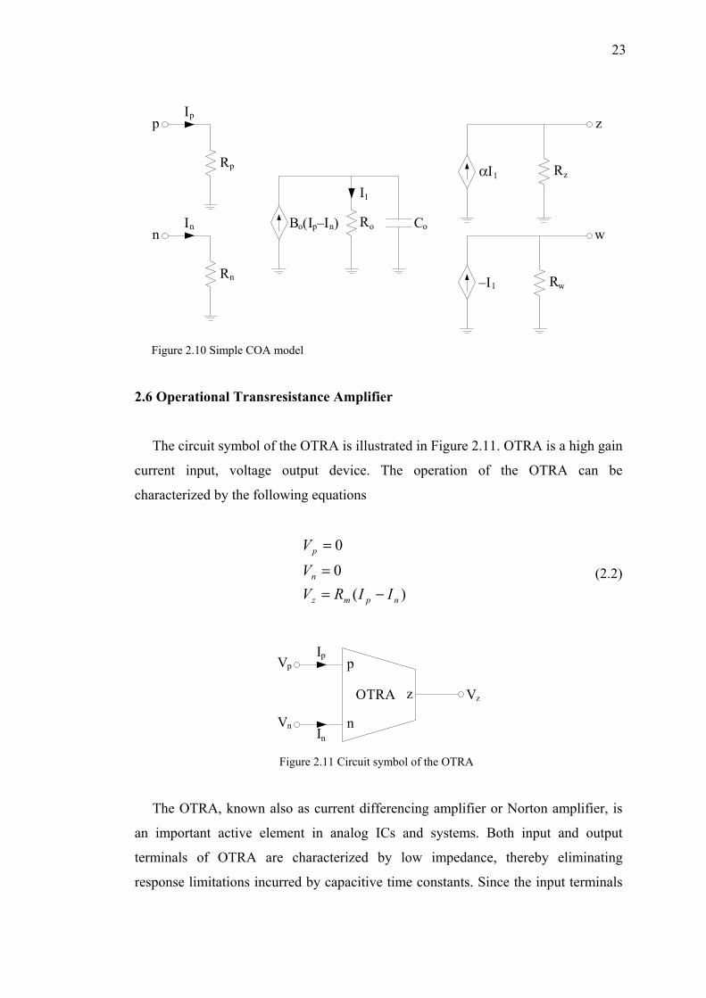
A simple model for the COA is shown in Figure 2.10. This model takes into
consideration some basic non-idealities of the COA. Different from the ideal
constitutive relation given in Equation (2.1), the voltages at the input terminals of a
real COA are not exactly equal to zero. This non-ideal effect has been represented in
the model of Figure 2.10 by two input resistance Rp and Rn which have small values.
On the other hand, practically the open loop current gain, B, is finite and frequency
dependent as oppose to the ideal case. The inner stage of the model represents this
non-ideality. It contains a differential current-control current source, a resistor and a
capacitor. For simplicity, a single-pole model is considered for the open loop current
gain in Figure 2.10. The final stage stands for the non-ideal output resistances Rz, Rw;
and also for the current tracking error between the two output terminals represented
by α which is very close to unity.
23
p
Rp
Ip
n
Rn
In Bo(Ip–In) Co
z
I1
Ro
Rw
αI1
–I1
w
Rz
Figure 2.10 Simple COA model
2.6 Operational Transresistance Amplifier
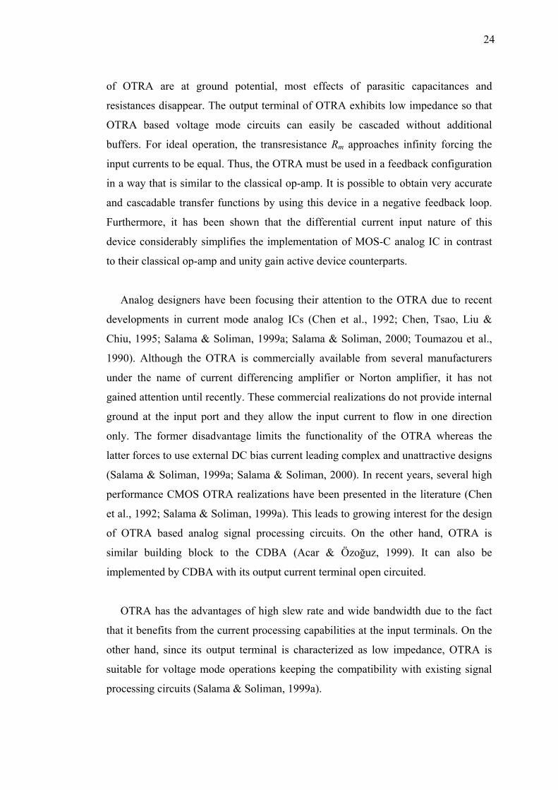
The circuit symbol of the OTRA is illustrated in Figure 2.11. OTRA is a high gain
current input, voltage output device. The operation of the OTRA can be
characterized by the following equations
)(00
npmz
n
p
IIRVVV
−==
=
(2.2)
Ip
In
Vp
Vn
OTRA
p
n
z Vz
Figure 2.11 Circuit symbol of the OTRA
The OTRA, known also as current differencing amplifier or Norton amplifier, is
an important active element in analog ICs and systems. Both input and output
terminals of OTRA are characterized by low impedance, thereby eliminating
response limitations incurred by capacitive time constants. Since the input terminals
24
of OTRA are at ground potential, most effects of parasitic capacitances and
resistances disappear. The output terminal of OTRA exhibits low impedance so that
OTRA based voltage mode circuits can easily be cascaded without additional
buffers. For ideal operation, the transresistance Rm approaches infinity forcing the
input currents to be equal. Thus, the OTRA must be used in a feedback configuration
in a way that is similar to the classical op-amp. It is possible to obtain very accurate
and cascadable transfer functions by using this device in a negative feedback loop.
Furthermore, it has been shown that the differential current input nature of this
device considerably simplifies the implementation of MOS-C analog IC in contrast
to their classical op-amp and unity gain active device counterparts.
Analog designers have been focusing their attention to the OTRA due to recent
developments in current mode analog ICs (Chen et al., 1992; Chen, Tsao, Liu &
Chiu, 1995; Salama & Soliman, 1999a; Salama & Soliman, 2000; Toumazou et al.,
1990). Although the OTRA is commercially available from several manufacturers
under the name of current differencing amplifier or Norton amplifier, it has not
gained attention until recently. These commercial realizations do not provide internal
ground at the input port and they allow the input current to flow in one direction
only. The former disadvantage limits the functionality of the OTRA whereas the
latter forces to use external DC bias current leading complex and unattractive designs
(Salama & Soliman, 1999a; Salama & Soliman, 2000). In recent years, several high
performance CMOS OTRA realizations have been presented in the literature (Chen
et al., 1992; Salama & Soliman, 1999a). This leads to growing interest for the design
of OTRA based analog signal processing circuits. On the other hand, OTRA is
similar building block to the CDBA (Acar & Özoğuz, 1999). It can also be
implemented by CDBA with its output current terminal open circuited.
OTRA has the advantages of high slew rate and wide bandwidth due to the fact
that it benefits from the current processing capabilities at the input terminals. On the
other hand, since its output terminal is characterized as low impedance, OTRA is
suitable for voltage mode operations keeping the compatibility with existing signal
processing circuits (Salama & Soliman, 1999a).
25
p
Rp
Ip
n
Rn
In Rmo(Ip–In)+_
Ro
Co V1+_
RzzV1
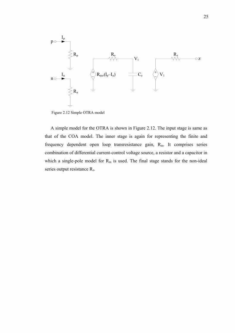
Figure 2.12 Simple OTRA model
A simple model for the OTRA is shown in Figure 2.12. The input stage is same as
that of the COA model. The inner stage is again for representing the finite and
frequency dependent open loop transresistance gain, Rm. It comprises series
combination of differential current-control voltage source, a resistor and a capacitor in
which a single-pole model for Rm is used. The final stage stands for the non-ideal
series output resistance Rz.
CHAPTER THREE
CMOS REALIZATION EXAMPLES FOR COA
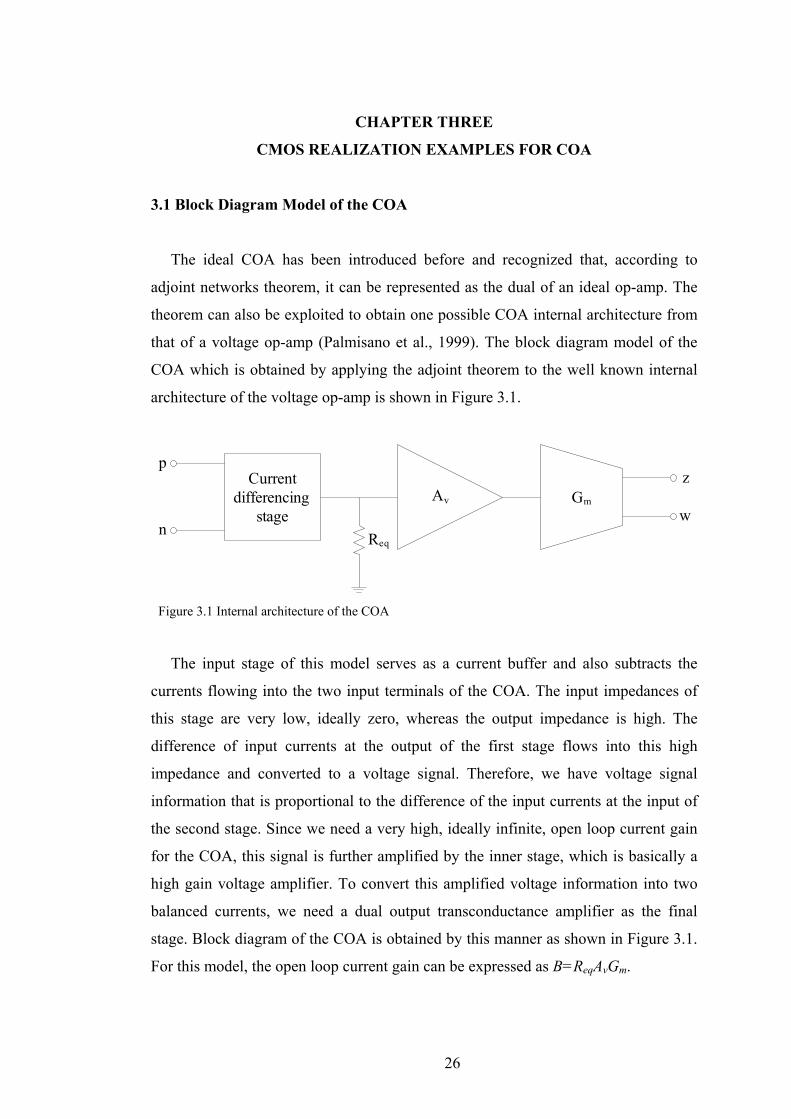
3.1 Block Diagram Model of the COA
The ideal COA has been introduced before and recognized that, according to
adjoint networks theorem, it can be represented as the dual of an ideal op-amp. The
theorem can also be exploited to obtain one possible COA internal architecture from
that of a voltage op-amp (Palmisano et al., 1999). The block diagram model of the
COA which is obtained by applying the adjoint theorem to the well known internal
architecture of the voltage op-amp is shown in Figure 3.1.
Gm
z
w
p
n
Av
Currentdifferencing
stageReq
Figure 3.1 Internal architecture of the COA
The input stage of this model serves as a current buffer and also subtracts the
currents flowing into the two input terminals of the COA. The input impedances of
this stage are very low, ideally zero, whereas the output impedance is high. The
difference of input currents at the output of the first stage flows into this high
impedance and converted to a voltage signal. Therefore, we have voltage signal
information that is proportional to the difference of the input currents at the input of
the second stage. Since we need a very high, ideally infinite, open loop current gain
for the COA, this signal is further amplified by the inner stage, which is basically a
high gain voltage amplifier. To convert this amplified voltage information into two
balanced currents, we need a dual output transconductance amplifier as the final
stage. Block diagram of the COA is obtained by this manner as shown in Figure 3.1.
For this model, the open loop current gain can be expressed as B=ReqAvGm.
26
27
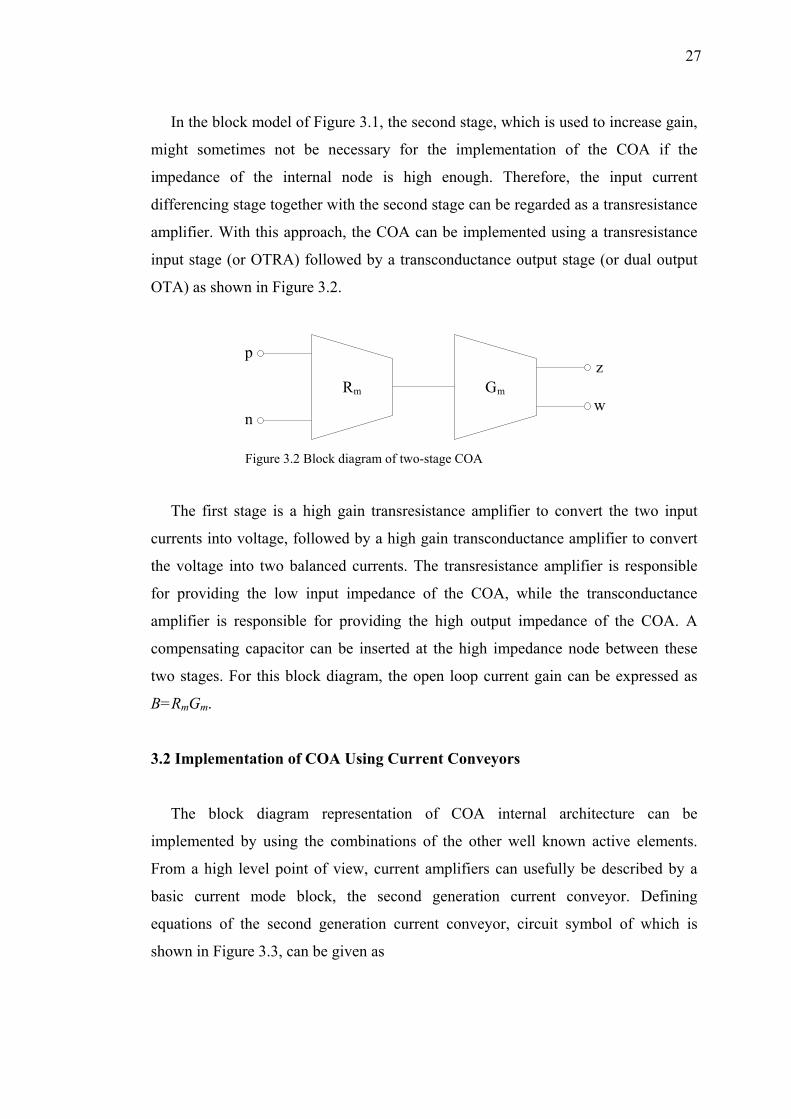
In the block model of Figure 3.1, the second stage, which is used to increase gain,
might sometimes not be necessary for the implementation of the COA if the
impedance of the internal node is high enough. Therefore, the input current
differencing stage together with the second stage can be regarded as a transresistance
amplifier. With this approach, the COA can be implemented using a transresistance
input stage (or OTRA) followed by a transconductance output stage (or dual output
OTA) as shown in Figure 3.2.
Gm
z
wRm
p
n
Figure 3.2 Block diagram of two-stage COA
The first stage is a high gain transresistance amplifier to convert the two input
currents into voltage, followed by a high gain transconductance amplifier to convert
the voltage into two balanced currents. The transresistance amplifier is responsible
for providing the low input impedance of the COA, while the transconductance
amplifier is responsible for providing the high output impedance of the COA. A
compensating capacitor can be inserted at the high impedance node between these
two stages. For this block diagram, the open loop current gain can be expressed as
B=RmGm.
3.2 Implementation of COA Using Current Conveyors
The block diagram representation of COA internal architecture can be
implemented by using the combinations of the other well known active elements.
From a high level point of view, current amplifiers can usefully be described by a
basic current mode block, the second generation current conveyor. Defining
equations of the second generation current conveyor, circuit symbol of which is
shown in Figure 3.3, can be given as
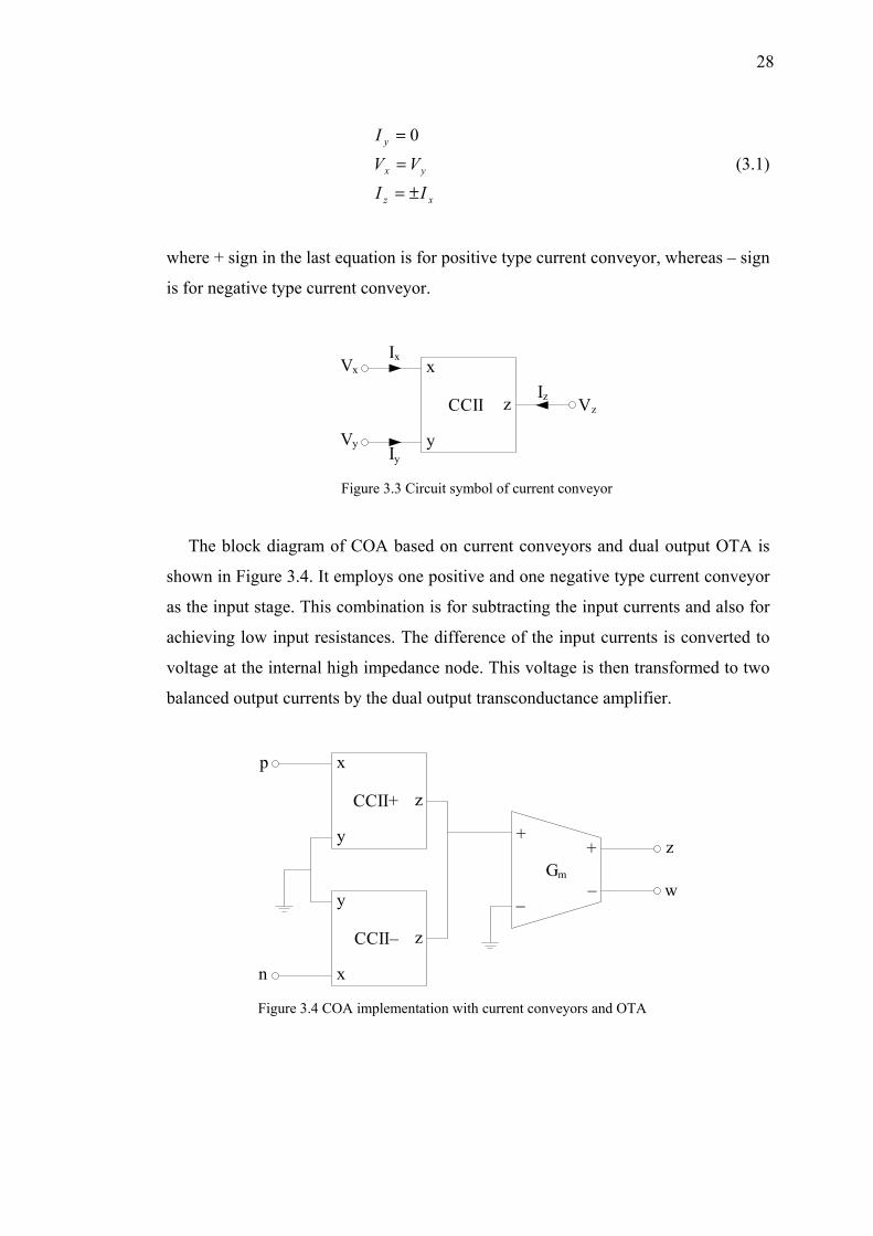
28
xz
yx
y
II
VV
I
±=
=
= 0
(3.1)
where + sign in the last equation is for positive type current conveyor, whereas – sign
is for negative type current conveyor.
Ix
Iy
Vx
Vy
CCII
x
y
z VzIz
Figure 3.3 Circuit symbol of current conveyor
The block diagram of COA based on current conveyors and dual output OTA is
shown in Figure 3.4. It employs one positive and one negative type current conveyor
as the input stage. This combination is for subtracting the input currents and also for
achieving low input resistances. The difference of the input currents is converted to
voltage at the internal high impedance node. This voltage is then transformed to two
balanced output currents by the dual output transconductance amplifier.
p
CCII+
x
y
z
n
CCII–
y
x
z
Gm
+
_
+
_
z
w
Figure 3.4 COA implementation with current conveyors and OTA
29
The output transconductance stage in Figure 3.4 can also be implemented using a
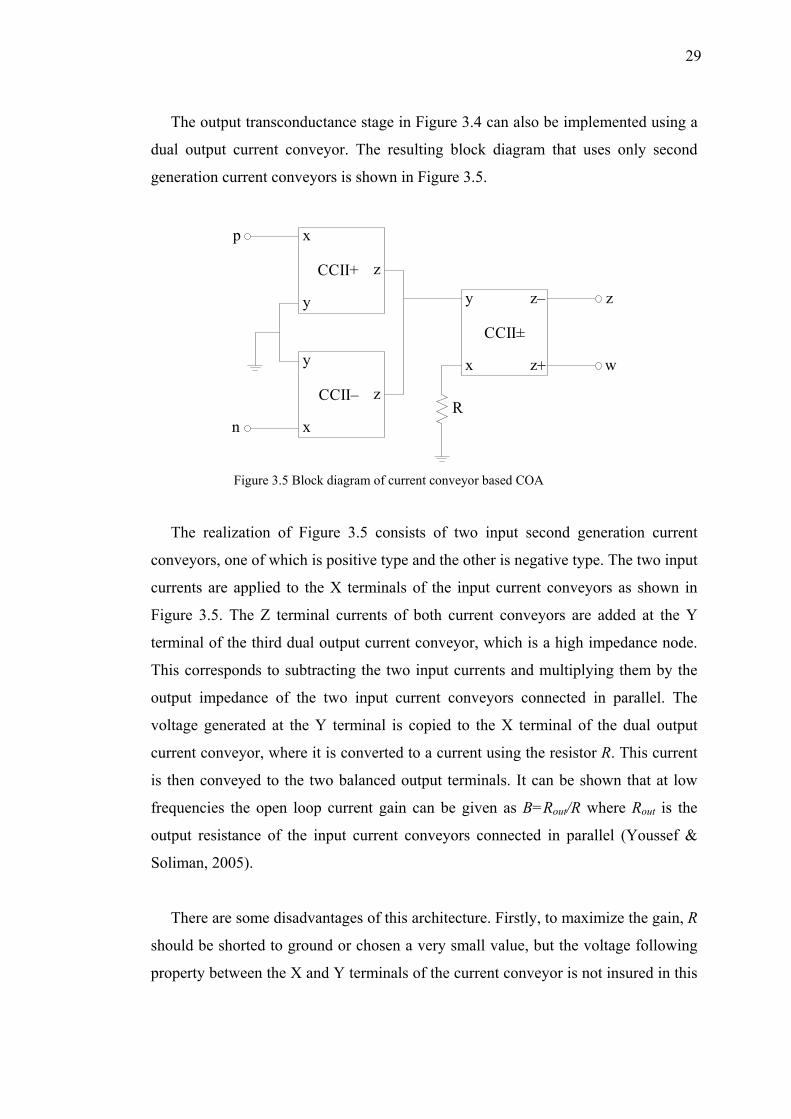
dual output current conveyor. The resulting block diagram that uses only second
generation current conveyors is shown in Figure 3.5.
p
CCII+
x
y
z
n
CCII–
y
x
z
z
w
CCII±
y
x
z–
z+
R
Figure 3.5 Block diagram of current conveyor based COA
The realization of Figure 3.5 consists of two input second generation current
conveyors, one of which is positive type and the other is negative type. The two input
currents are applied to the X terminals of the input current conveyors as shown in
Figure 3.5. The Z terminal currents of both current conveyors are added at the Y
terminal of the third dual output current conveyor, which is a high impedance node.
This corresponds to subtracting the two input currents and multiplying them by the
output impedance of the two input current conveyors connected in parallel. The
voltage generated at the Y terminal is copied to the X terminal of the dual output
current conveyor, where it is converted to a current using the resistor R. This current
is then conveyed to the two balanced output terminals. It can be shown that at low
frequencies the open loop current gain can be given as B=Rout/R where Rout is the
output resistance of the input current conveyors connected in parallel (Youssef &
Soliman, 2005).
There are some disadvantages of this architecture. Firstly, to maximize the gain, R
should be shorted to ground or chosen a very small value, but the voltage following
property between the X and Y terminals of the current conveyor is not insured in this
30
case. Secondly, the output resistance of the input current conveyors is reduced due to
their parallel connection. Finally, matching the two current conveyor blocks is not an
easy design task due to their different polarities (Youssef & Soliman, 2005).
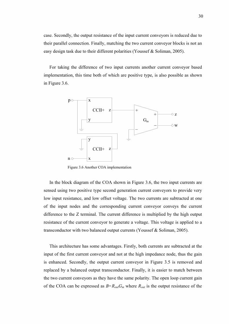
For taking the difference of two input currents another current conveyor based
implementation, this time both of which are positive type, is also possible as shown
in Figure 3.6.
p
CCII+
x
y
z
n
CCII+
y
x
z
Gm
+
_
+
_
z
w
Figure 3.6 Another COA implementation
In the block diagram of the COA shown in Figure 3.6, the two input currents are
sensed using two positive type second generation current conveyors to provide very
low input resistance, and low offset voltage. The two currents are subtracted at one
of the input nodes and the corresponding current conveyor conveys the current
difference to the Z terminal. The current difference is multiplied by the high output
resistance of the current conveyor to generate a voltage. This voltage is applied to a
transconductor with two balanced output currents (Youssef & Soliman, 2005).
This architecture has some advantages. Firstly, both currents are subtracted at the
input of the first current conveyor and not at the high impedance node, thus the gain
is enhanced. Secondly, the output current conveyor in Figure 3.5 is removed and
replaced by a balanced output transconductor. Finally, it is easier to match between
the two current conveyors as they have the same polarity. The open loop current gain
of the COA can be expressed as B=RoutGm where Rout is the output resistance of the
31
current conveyor. From the above equation, it is evident that the block diagram in
Figure 3.6 leads to the same gain when cascading a transresistance and
transconductance amplifiers, but in this case simple current conveyors replace the
transresistance amplifier (Youssef&Soliman, 2005).
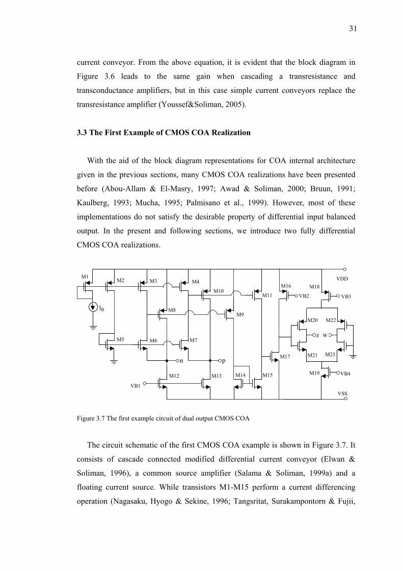
3.3 The First Example of CMOS COA Realization
With the aid of the block diagram representations for COA internal architecture
given in the previous sections, many CMOS COA realizations have been presented
before (Abou-Allam & El-Masry, 1997; Awad & Soliman, 2000; Bruun, 1991;
Kaulberg, 1993; Mucha, 1995; Palmisano et al., 1999). However, most of these
implementations do not satisfy the desirable property of differential input balanced
output. In the present and following sections, we introduce two fully differential
CMOS COA realizations.
IB
M1 M2 M3 M4
M5 M6
M10
M7
M8
p
M11
M16
M12 M13 M14 M15
M17
M18
M19
M20 M22
M21 M23n
z w
VDD
VSSVB1
VB4
VB3VB2
M9
Figure 3.7 The first example circuit of dual output CMOS COA
The circuit schematic of the first CMOS COA example is shown in Figure 3.7. It
consists of cascade connected modified differential current conveyor (Elwan &
Soliman, 1996), a common source amplifier (Salama & Soliman, 1999a) and a
floating current source. While transistors M1-M15 perform a current differencing
operation (Nagasaku, Hyogo & Sekine, 1996; Tangsritat, Surakampontorn & Fujii,
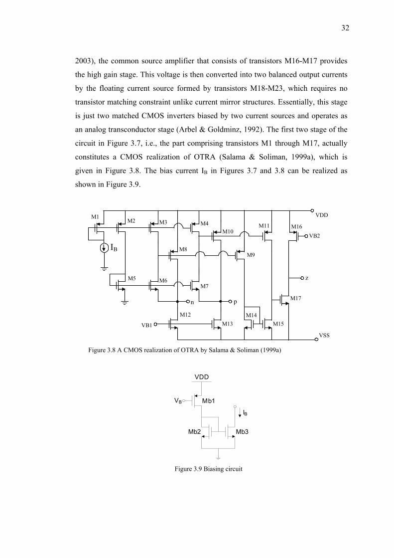
32
2003), the common source amplifier that consists of transistors M16-M17 provides
the high gain stage. This voltage is then converted into two balanced output currents
by the floating current source formed by transistors M18-M23, which requires no
transistor matching constraint unlike current mirror structures. Essentially, this stage
is just two matched CMOS inverters biased by two current sources and operates as
an analog transconductor stage (Arbel & Goldminz, 1992). The first two stage of the
circuit in Figure 3.7, i.e., the part comprising transistors M1 through M17, actually
constitutes a CMOS realization of OTRA (Salama & Soliman, 1999a), which is
given in Figure 3.8. The bias current IB in Figures 3.7 and 3.8 can be realized as
shown in Figure 3.9.
IB
M1 M2 M3 M4
M5 M6
M10
M7
M8
p
M11 M16
M12M13
M14M15
M17 n
VDD
VSS
VB1
VB2
M9
z
Figure 3.8 A CMOS realization of OTRA by Salama & Soliman (1999a)
Mb3
VDD
IB
VB Mb1
Mb2
Figure 3.9 Biasing circuit
33
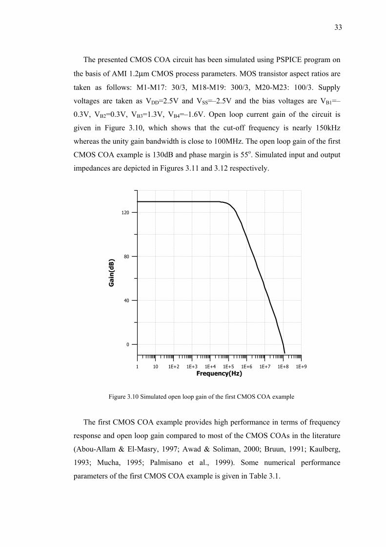
The presented CMOS COA circuit has been simulated using PSPICE program on
the basis of AMI 1.2µm CMOS process parameters. MOS transistor aspect ratios are
taken as follows: M1-M17: 30/3, M18-M19: 300/3, M20-M23: 100/3. Supply
voltages are taken as VDD=2.5V and VSS=–2.5V and the bias voltages are VB1=–
0.3V, VB2=0.3V, VB3=1.3V, VB4=–1.6V. Open loop current gain of the circuit is
given in Figure 3.10, which shows that the cut-off frequency is nearly 150kHz
whereas the unity gain bandwidth is close to 100MHz. The open loop gain of the first
CMOS COA example is 130dB and phase margin is 55o. Simulated input and output
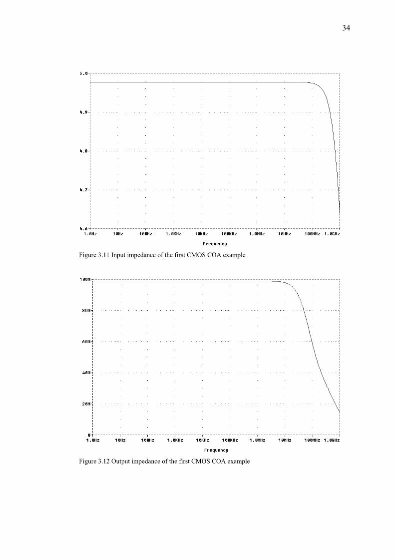
impedances are depicted in Figures 3.11 and 3.12 respectively.
1 10 1E+2 1E+3 1E+4 1E+5 1E+6 1E+7 1E+8 1E+9Frequency(Hz)
0
40
80
120
Gai
n(dB
)
Figure 3.10 Simulated open loop gain of the first CMOS COA example
The first CMOS COA example provides high performance in terms of frequency
response and open loop gain compared to most of the CMOS COAs in the literature
(Abou-Allam & El-Masry, 1997; Awad & Soliman, 2000; Bruun, 1991; Kaulberg,
1993; Mucha, 1995; Palmisano et al., 1999). Some numerical performance
parameters of the first CMOS COA example is given in Table 3.1.
34
Figure 3.11 Input impedance of the first CMOS COA example
Figure 3.12 Output impedance of the first CMOS COA example

35
Table 3.1 Some numerical performance parameters of the first CMOS COA example
Open loop current gain 130 dB
Unity gain bandwidth 100 MHz
Cut-off frequency 150 kHz
Phase margin 55°
Slew rate 15 µA/ns
Input resistances 5 Ω
Output resistances 100 MΩ
3.4 The Second Example of CMOS COA Realization
The second example of CMOS COA realization is shown in Figure 3.13. It is
constructed by cascading an OTRA, a voltage amplifier and a dual output OTA. The
first stage, composed of transistors M1 through M20, was originally proposed for the
realization of CDBA (Toker, Özoğuz, Çiçekoğlu & Acar, 2000). It can also be used
as the OTRA with open circuited z terminal of CDBA. It consists of a differential
current controlled current source followed by a voltage buffer. The second stage
(M21-M22), which is a common source amplifier, provides extra gain. The final
stage is the floating current source (Arbel & Goldminz, 1992) formed by transistors
M23-M28 and operates as an analog transconductor. The bias currents IB in Figure
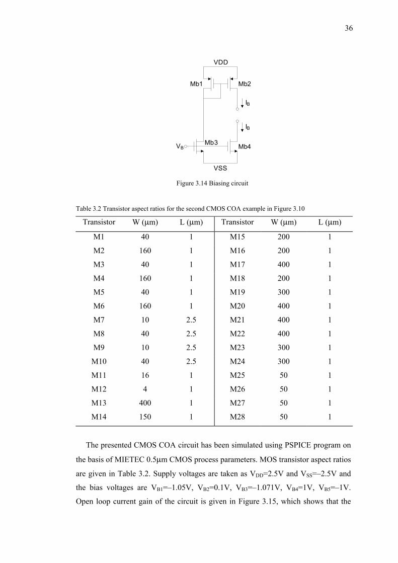
3.13 can be realized as shown in Figure 3.14.
M21
M22
M23
M24
M25 M27
M26 M28
z w
VDD
VSS
VB5
VB4VB3M13
M14
M15
M17M16
M19
M20
M18
M7
M8
M3
M4
M1
M2
M9
M12
M11
M10
pM5
M6
IB
IB
n
VB2
VB1
Figure 3.13 The second example circuit of dual output CMOS COA
36
Mb4
VDD
IB
VB
Mb1
Mb3
Mb2
VSS
IB
Figure 3.14 Biasing circuit
Table 3.2 Transistor aspect ratios for the second CMOS COA example in Figure 3.10
Transistor W (µm) L (µm) Transistor W (µm) L (µm)
M1 40 1 M15 200 1
M2 160 1 M16 200 1
M3 40 1 M17 400 1
M4 160 1 M18 200 1
M5 40 1 M19 300 1
M6 160 1 M20 400 1
M7 10 2.5 M21 400 1
M8 40 2.5 M22 400 1
M9 10 2.5 M23 300 1
M10 40 2.5 M24 300 1
M11 16 1 M25 50 1
M12 4 1 M26 50 1
M13 400 1 M27 50 1
M14 150 1 M28 50 1
The presented CMOS COA circuit has been simulated using PSPICE program on
the basis of MIETEC 0.5µm CMOS process parameters. MOS transistor aspect ratios
are given in Table 3.2. Supply voltages are taken as VDD=2.5V and VSS=–2.5V and
the bias voltages are VB1=–1.05V, VB2=0.1V, VB3=–1.071V, VB4=1V, VB5=–1V.
Open loop current gain of the circuit is given in Figure 3.15, which shows that the

37
cut-off frequency is nearly 200kHz whereas the unity gain bandwidth is close to
230MHz. The open loop gain of the second CMOS COA example is 110dB and
phase margin is 45o. Simulated input and output impedances are depicted in Figures
3.16 and 3.17 respectively. Some numerical performance parameters of the second
CMOS COA example is given in Table 3.3.
1E+0 1E+1 1E+2 1E+3 1E+4 1E+5 1E+6 1E+7 1E+8 1E+9Frequency (Hz)
0
40
80
120
Gai
n (d
B)
Figure 3.15 Simulated open loop gain of the second CMOS COA example
Table 3.3 Some numerical performance parameters of the second CMOS COA example
Open loop current gain 110 dB
Unity gain bandwidth 230 MHz
Cut-off frequency 200 kHz
Phase margin 45°
Slew rate 20 µA/ns
Input resistances 400 Ω
Output resistances 100 MΩ

38
Figure 3.16 Input impedance of the second CMOS COA example
Figure 3.17 Output impedance of the second CMOS COA example
CHAPTER FOUR
ANALOG CIRCUIT DESIGN USING COA
In this Chapter, we present some new circuits as the applications of the CMOS
COA realizations introduced in Chapter 3. We start with a first order allpass filter,
which includes a bare minimum number of passive components. Then a biquadratic
filter configuration is presented. Second order lowpass, highpass, bandpass, and
notch filters can be realized using this configuration. Finally, a sinusoidal oscillator
configuration, which allows obtaining ten different oscillators, is presented.
All of these filter and oscillator circuits employ only one COA as the active
element. This feature is advantageous in terms of power consumption. They also
enjoy the properties of the COA presented in Chapter 2. The proposed filters and
oscillators have high output impedances since the output current is taken from one of
the output terminals of the COA that is characterized as high impedance. This
property enables the filters to be cascaded without the addition of a buffer. Also, the
high output impedance of the oscillators allows for driving the loads without the
addition of a buffer. On the other hand, the circuits are insensitive to parasitic input
capacitances and input resistances due to internally grounded input terminals of
COA.
4.1 Current Mode First Order Allpass Filters
Allpass filters are one of the most commonly used filter types of all. They are
generally used for introducing a frequency dependent delay while keeping the
amplitude of the input signal constant over the desired frequency range. Other types
of active circuits such as oscillators and high Q bandpass filters are also realized by
using allpass filters (D. J. Comer & McDermid, 1968; D. T. Comer, D. J. Comer &
Gonzalez, 1997; Moschytz, 1972; Schauman & Van Valkenburg, 2001; Tarmy &
Ghausi, 1970). Current mode filters reported in literature, either do not offer allpass
configurations at all, or are excess in the number of components and require
component matching constraints (Çam, Çiçekoğlu, Gülsoy & Kuntman, 2000;
39
40
Chang, 1991a; Higashimura, 1991; Higashimura & Fukiu, 1988; Liu & Hwang,
1997). Recently, a CDBA based first order current mode allpass filter configuration
is proposed (Toker et al., 2000). The circuit uses single CDBA, a resistor and a
capacitor, which are of minimum number. However, the transfer function of the
circuit is sensitive to current tracking error of the CDBA and the accuracy of CMOS
CDBA depends on matching of MOS transistors. It is a well known fact that open
loop circuits are less accurate compared to their high gain counterparts. On the other
hand, COA is a high gain current-input, current-output device. Using this device in
negative feedback configuration makes it possible to obtain very accurate transfer
functions (Awad & Soliman, 2000; Mucha, 1995). In this section, COA based
current mode first order allpass filter configuration is presented (Kılınç & Çam,
2003a, 2003b, 2004a). The circuit uses single COA, a resistor and a capacitor, which
are of minimum number. A sinusoidal quadrature oscillator is implemented to show
the usefulness of the filter configuration as an illustrating example.
p
n
z
w
COA
y1
y2
Iin Iout
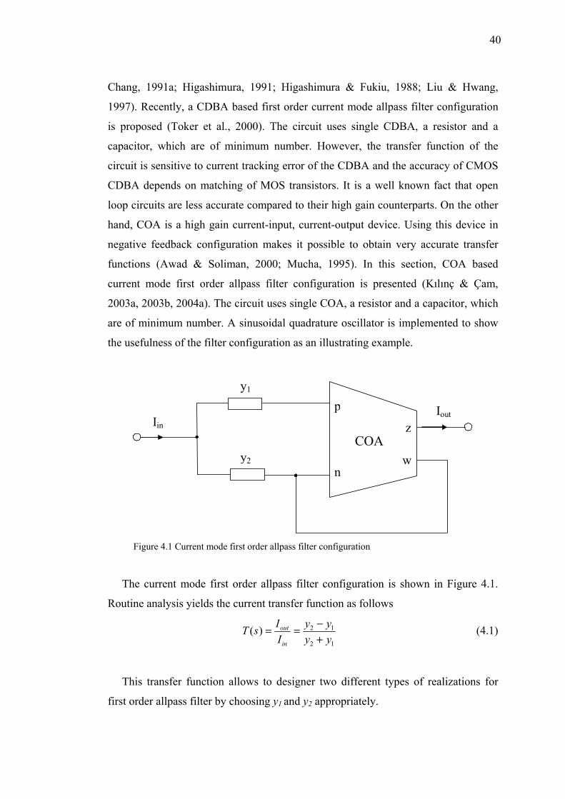
Figure 4.1 Current mode first order allpass filter configuration
The current mode first order allpass filter configuration is shown in Figure 4.1.
Routine analysis yields the current transfer function as follows
12
12)(yyyy
IIsT
in
out
+−== (4.1)
This transfer function allows to designer two different types of realizations for
first order allpass filter by choosing y1 and y2 appropriately.
41
For y1=G and y2=sC the transfer function becomes
GsCGsC
II
sTin
out
+−==)(1 (4.2)
For y1 = sC and y2 = G the transfer function becomes
GsCGsC
II
sTin
out
+−−==)(2 (4.3)
Thus, both inverting and noninverting types of first order current mode allpass
filters are realized using only a single COA, a resistor and a capacitor without
imposing any passive element matching condition. The outputs of the filters exhibit
high impedance so that the synthesized current mode filters can be cascaded without
additional buffers. Most of the effects of parasitic input impedances disappear for the
presented allpass filters due to internally grounded input terminals of COA. The
allpass filters have the following phase responses
−=
−°=
GCnarcta
GCnarcta
ωωϕ
ωωϕ
2)(
2180)(
2
1
(4.4)
As it can be seen from the defining equation of the COA given in Chapter 2, there
are two main non-ideal effects. The first one is the current tracking error between z
and w terminals which can be represented by α ( Iz = α Iw ). The other non-ideality is
nonzero voltage at p and n terminals. This can be considered by connecting parasitic
admittances yp and yn between the ground and p and n terminals, respectively.
Routine analysis yields modified transfer function to be as follows
)()(1)(
2121
2121
pnpnpn
nppnpn
in
out
yyyyyyyyyyyyyyyyyyyy
II
sT−++−+−
==α
(4.5)
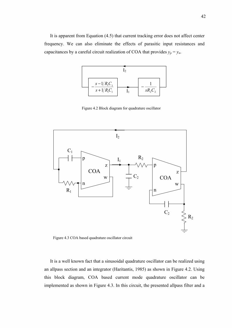
42
It is apparent from Equation (4.5) that current tracking error does not affect center
frequency. We can also eliminate the effects of parasitic input resistances and
capacitances by a careful circuit realization of COA that provides yp = yn.
22
1CsR
− 11
11
11
CRsCRs
+−
− I1
I2
Figure 4.2 Block diagram for quadrature oscillator
C1
R1
I1
I2
p
n
z
w
COAp
n
z
w
COA
C2
C2
R2
R2
Figure 4.3 COA based quadrature oscillator circuit
It is a well known fact that a sinusoidal quadrature oscillator can be realized using
an allpass section and an integrator (Haritantis, 1985) as shown in Figure 4.2. Using
this block diagram, COA based current mode quadrature oscillator can be
implemented as shown in Figure 4.3. In this circuit, the presented allpass filter and a
43
current mode integrator employing a COA with two matched resistors and capacitors
are used. For providing a sinusoidal oscillation the loop gain of the circuit is set to
unity at ωjs = , i.e.
1111
2211
11 =
−
+−
−= ωjs
CsRCRsCRs (4.6)
From Equation (4.6) oscillation condition and frequency can be found
respectively as
2211 CRCR = (4.7)
22110
1CRCR
=ω (4.8)
For simplicity, if we choose and , oscillation condition
is satisfied and oscillation frequency becomes
RRR == 21 CCC == 21
RC1
0 =ω (4.9)
The sensitivity analysis of this oscillator shows that
210
2
0
1
0
2
0
1−==== ωωωω
CCRR SSSS
which are all less than unity in magnitude.
To verify the theoretical study, the first order allpass filter was constructed and
simulated using PSPICE program on the basis of AMI 1.2µm CMOS process
parameters. For this purpose, passive components were chosen as R=10kΩ and
C=10pF, which results in a 1.59MHz center frequency. The PSPICE simulations
were performed using the CMOS realization of the COA given in Figure 3.7. The
supply voltages were taken as VDD=2.5V and VSS=–2.5V. Simulation results of the
filter response with ideal and CMOS COA are given in Figure 4.4, which are in good
agreement with the predicted theory. Figure 4.5 shows the time domain response of
the filter. A sinusoidal input at a frequency of 1MHz was applied to the allpass
network constructed with above mentioned passive element values. This causes a

44
176ns time delay at the output of the filter corresponding to a 63° phase difference
which is very close to the theoretical value (64°).
Figure 4.4 Simulation result of the allpass filter; ideal COA, CMOS COA
Figure 4.5 Simulated time domain response of the allpass filter
Quadrature oscillator employing the presented allpass filter has also been
simulated using PSPICE. In this simulation, all resistances and capacitances were
taken as 10kΩ and 10pF respectively which results in a 1.59MHz oscillation
frequency. The output waveforms of the oscillator are shown in Figure 4.6.
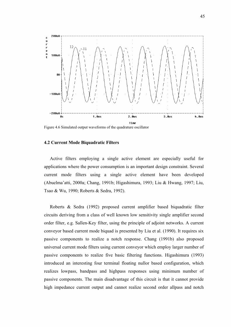
45
Figure 4.6 Simulated output waveforms of the quadrature oscillator
4.2 Current Mode Biquadratic Filters
Active filters employing a single active element are especially useful for
applications where the power consumption is an important design constraint. Several
current mode filters using a single active element have been developed
(Abuelma’atti, 2000a; Chang, 1991b; Higashimura, 1993; Liu & Hwang, 1997; Liu,
Tsao & Wu, 1990; Roberts & Sedra, 1992).
Roberts & Sedra (1992) proposed current amplifier based biquadratic filter
circuits deriving from a class of well known low sensitivity single amplifier second
order filter, e.g. Sallen-Key filter, using the principle of adjoint networks. A current
conveyor based current mode biquad is presented by Liu et al. (1990). It requires six
passive components to realize a notch response. Chang (1991b) also proposed
universal current mode filters using current conveyor which employ larger number of
passive components to realize five basic filtering functions. Higashimura (1993)
introduced an interesting four terminal floating nullor based configuration, which
realizes lowpass, bandpass and highpass responses using minimum number of
passive components. The main disadvantage of this circuit is that it cannot provide
high impedance current output and cannot realize second order allpass and notch
46
responses. Moreover, an additional current buffer is needed to sense the output
current. Liu & Hwang (1997) proposed a configuration to reduce the required
number of passive components to at most seven. A universal current mode filter
using single four terminal floating nullor is presented by Abuelma’atti (2000a). It
provides independent adjustment of natural frequency, quality factor and gain of the
filter by allowing the use of large number of passive components deliberately.
The active elements in these filters have finite open loop gains. However, the use
of high open loop gain COA allows obtaining accurate transfer functions in terms of
accuracy, noise and distortion. In this section, a cascadable current mode filter
configuration employing single COA is presented (Kılınç & Çam, 2003c, 2003d).
Realizations of current mode second order lowpass, highpass, bandpass and notch
filters are possible using this configuration. The required number of passive
components for the presented biquads is four, namely two resistors and two
capacitors, which is minimum. The output of the general filter configuration exhibits
high output impedance so that the synthesized current mode filters can be cascaded
without additional buffers. Most of the effects of parasitic input impedances
disappear due to internally grounded input terminals of COA.
n
p
w
z
COA
Y1
Y2
Iin
Iout
Y3
Y4
Y5
Figure 4.7 Current mode general biquadratic filter configuration
47
The current mode general biquadratic filter configuration is shown in Figure 4.7.
Routine analysis yields the current transfer function as follows
)(])([])([
54324254231
4324254231
YYYYYYYYYYYYYYYYYYYYY
II
in
out
++−++−−++
= (4.10)
With proper selection of admittances in Equation (4.10), current mode second
order lowpass, highpass, bandpass and notch filters can be realized as described
below.
n
p
w
z
COA
G1
C2
Iin
Iout
G4
C5
Figure 4.8 Current mode second order lowpass filter
For the following choices of admittances
55
44
3
22
11
sCYGY
YsCYGY
==∞=
==
as shown in Figure 4.8, Equation (4.10) becomes
41245212
52
41245211 ])([
])([)(
GGsCGCCGsCCGGsCGCCG
sT++++
+−+= (4.11)
For G , transfer function reduces to 24521 )( CGCC =+
48
41242
52
411 2
)(GGsCGsCC
GGsT++
= (4.12)
The natural frequency and the quality factor of this lowpass filter can be
expressed as
52
41
CCGG
o =ω (4.13)
24
51
21
CGCG
Q = (4.14)
n
p
w
z
COA
C1
G2
Iin
Iout
C4
G5
Figure 4.9 Current mode second order highpass filter
If admittances are chosen as
55
44
3
22
11
GYsCY
YGYsCY
==∞=
==
the resultant circuit of which is shown in Figure 4.9, Equation (4.10) becomes
52421522
41
421522
412 ])[(
])[()(
GGsCGCGGsCCsCGCGGsCC
sT++++
−++= (4.15)
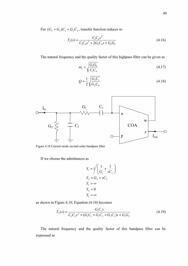
49
For ( , transfer function reduces to 42152 ) CGCGG =+
52422
41
241
2 2)(
GGsCGsCCsCCsT
++= (4.16)
The natural frequency and the quality factor of this highpass filter can be given as
41
52
CCGG
o =ω (4.17)
42
15
21
CGCG
Q = (4.18)
n
p
w
z
COA
G1Iin
Iout
C1
G2 C2
Figure 4.10 Current mode second order bandpass filter
If we choose the admittances as
∞==∞=
+=
+=
5
4
3
222
111
0
111
YYY
sCGYsCG
Y
as shown in Figure 4.10, Equation (4.10) becomes
211221112
21
113 )(
)(GGsCGCGCGsCC
sCGsT++++
= (4.19)
The natural frequency and the quality factor of this bandpass filter can be
expressed as
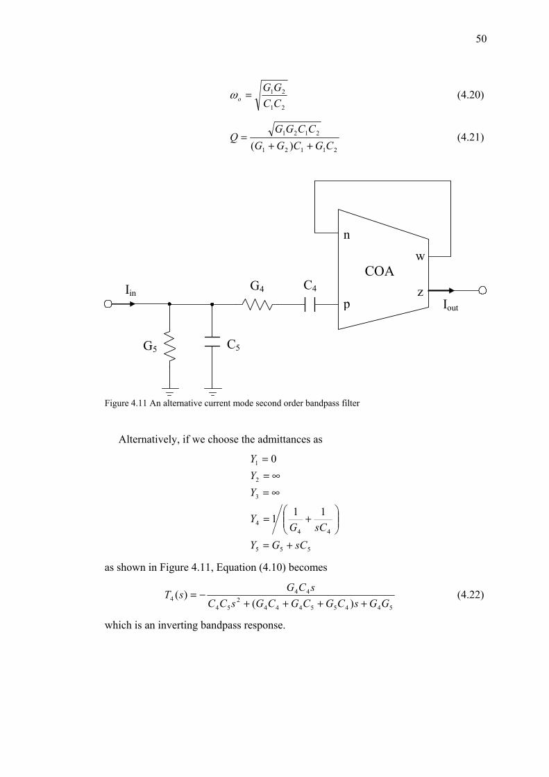
50
21
21
CCGG
o =ω (4.20)
21121
2121
)( CGCGGCCGG
Q++
= (4.21)
n
p
w
z
COA G4Iin
Iout
C4
G5 C5
Figure 4.11 An alternative current mode second order bandpass filter
Alternatively, if we choose the admittances as
555
444
3
2
1
111
0
sCGYsCG
Y
YYY
+=
+=
∞=∞=
=
as shown in Figure 4.11, Equation (4.10) becomes
544554442
54
444 )(
)(GGsCGCGCGsCC
sCGsT++++
−= (4.22)
which is an inverting bandpass response.
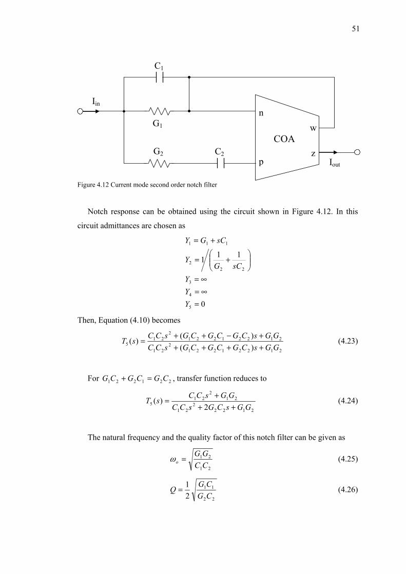
51
n
p
w
z
COA
C1
G2
Iin
Iout
C2
G1
Figure 4.12 Current mode second order notch filter
Notch response can be obtained using the circuit shown in Figure 4.12. In this
circuit admittances are chosen as
0
111
5
4
3
222
111
=∞=∞=
+=
+=
YYY
sCGY
sCGY
Then, Equation (4.10) becomes
212212212
21
212212212
215 )(
)()(GGsCGCGCGsCCGGsCGCGCGsCCsT
+++++−++
= (4.23)
For G , transfer function reduces to 221221 CGCGC =+
21222
21
212
215 2
)(GGsCGsCC
GGsCCsT++
+= (4.24)
The natural frequency and the quality factor of this notch filter can be given as
21
21
CCGG
o =ω (4.25)
22
11
21
CGCG
Q = (4.26)
52
Note that if we interchange the selections of Y1 and Y2, an inverting notch
response is obtained for , transfer function of which is given as 111221 CGCGCG =+
21112
21
212
215 2
)(GGsCGsCC
GGsCCsT++
+−= (4.27)
The sensitivity analysis is performed by the use of sensitivity definition of F with
respect to x as
xF
FxS F
x ∂∂= (4.28)
For the lowpass filter whose parameters are given in Equations (4.13) and (4.14)
sensitivity analysis yields
2/152415241==−=−==−=−== Q
CQC
QG
QGCCGG SSSSSSSS oooo ωωωω
For the highpass filter whose parameters are given in Equations (4.17) and (4.18)
sensitivity analysis yields
2/141524152=−===−=−=−== Q
CQC
QG
QGCCGG SSSSSSSS oooo ωωωω
For the bandpass filter whose parameters are given in Equations (4.20) and (4.21)
sensitivity analysis yields
2/12121=−=−== oooo
CCGG SSSS ωωωω
++−−=
21121
21112
)()(
21
1 CGCGGCGCGGS Q
G
+++−=
21121
21121
)()(
21
2 CGCGGCGCGGS Q
G
++++−=
21121
21121
)()(
21
1 CGCGGCGCGGS Q
C
++−+=
21121
21121
)()(
21
2 CGCGGCGCGGS Q
C
For the notch filter whose parameters are given in Equations (4.25) and (4.26)
sensitivity analysis yields
2/121212121=−==−==−=−== Q
CQC
QG
QGCCGG SSSSSSSS oooo ωωωω
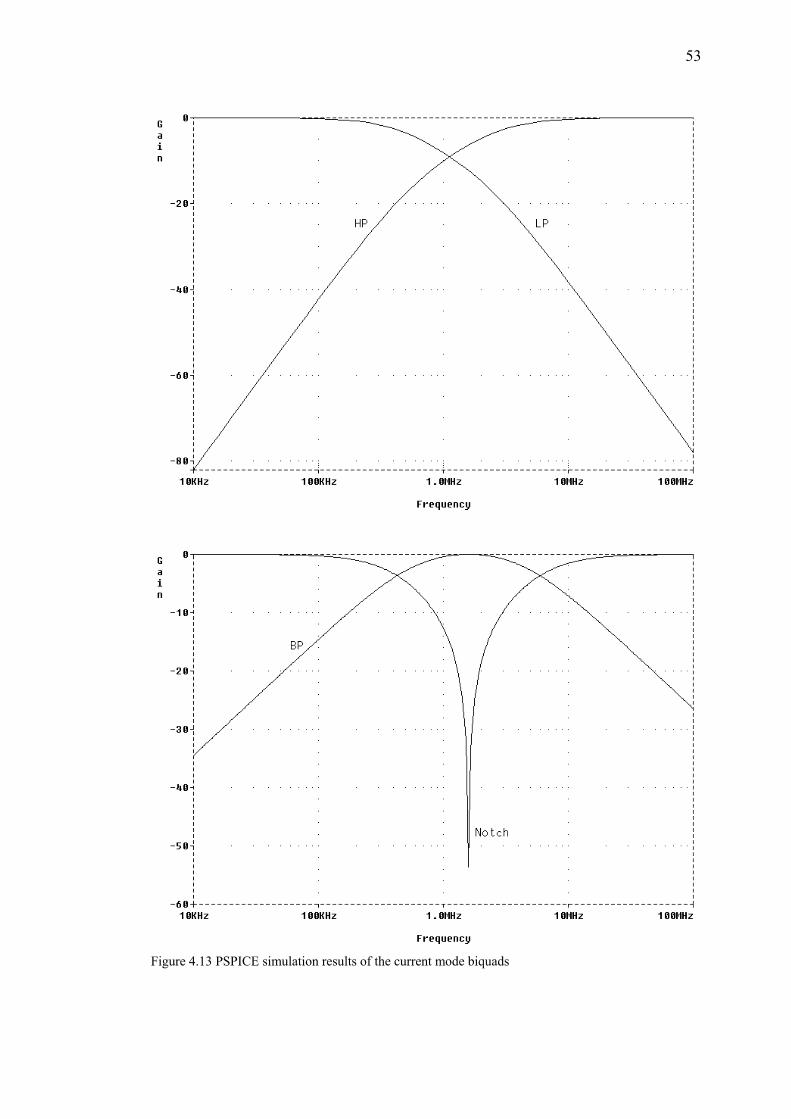
53
Figure 4.13 PSPICE simulation results of the current mode biquads
54
As it is evident from the analysis, sensitivities of natural frequencies and quality
factors of the filters with respect to passive components are no more than one half in
magnitude.
To verify the theoretical study, the presented biquadratic filters were constructed
and simulated using PSPICE program. Passive component values used in simulations
and resultant natural frequencies are given below.
Lowpass circuit: R1 = 2 kΩ, R4 = 1 kΩ, C2 = C5 = 100 pF, fo = 1.1254 MHz
Highpass circuit: R2 = R5 = 1 kΩ, C1 = 100 pF, C4 = 200 pF, fo = 1.1254 MHz
Bandpass circuit: R1 = R2 = 1 kΩ, C1 = C2 = 100 pF, fo = 1.5915 MHz
Notch circuit: R1 = 2 kΩ, R2 = 1 kΩ, C1 = 50 pF, C2 = 100 pF, fo = 1.5915 kHz
The presented filters have been simulated with PSPICE program on the basis of
MIETEC 0.5µm process parameters using the CMOS COA given in Figure 3.10. For
this simulation, supply voltages were taken as VDD=2.5V and VSS=–2.5V. Simulation
results of filter responses are given in Figure 4.13, which are in good agreement with
the predicted theory. In simulation, gain of the bandpass filter is multiplied by three.
4.3 Current Mode Sinusoidal Oscillators
The generation of sinusoidal waveforms is an important task for electronics
engineering. Oscillators are widely used in signal processing circuits,
communication, control and measurement systems. Many sinusoidal oscillators
employing op-amp have been reported up to now. However, as mentioned earlier, the
classical op-amp suffers from limited gain-bandwidth product affecting oscillation
condition and frequency of the oscillators designed by using op-amp. Therefore, they
remain unsatisfactory at higher frequencies (Budak, 1974). To overcome this
problem, several sinusoidal oscillators have been introduced which use OTA, current
conveyor, current feedback operational amplifier or four terminal floating nullor as
the active element (Abuelma’atti, 2000b; Abuelma’atti & Al-Zaher, 1999; Celma,
Martinez & Carlosena, 1992; Çam, Kuntman & Acar, 1998; Çam, Toker, Çiçekoğlu
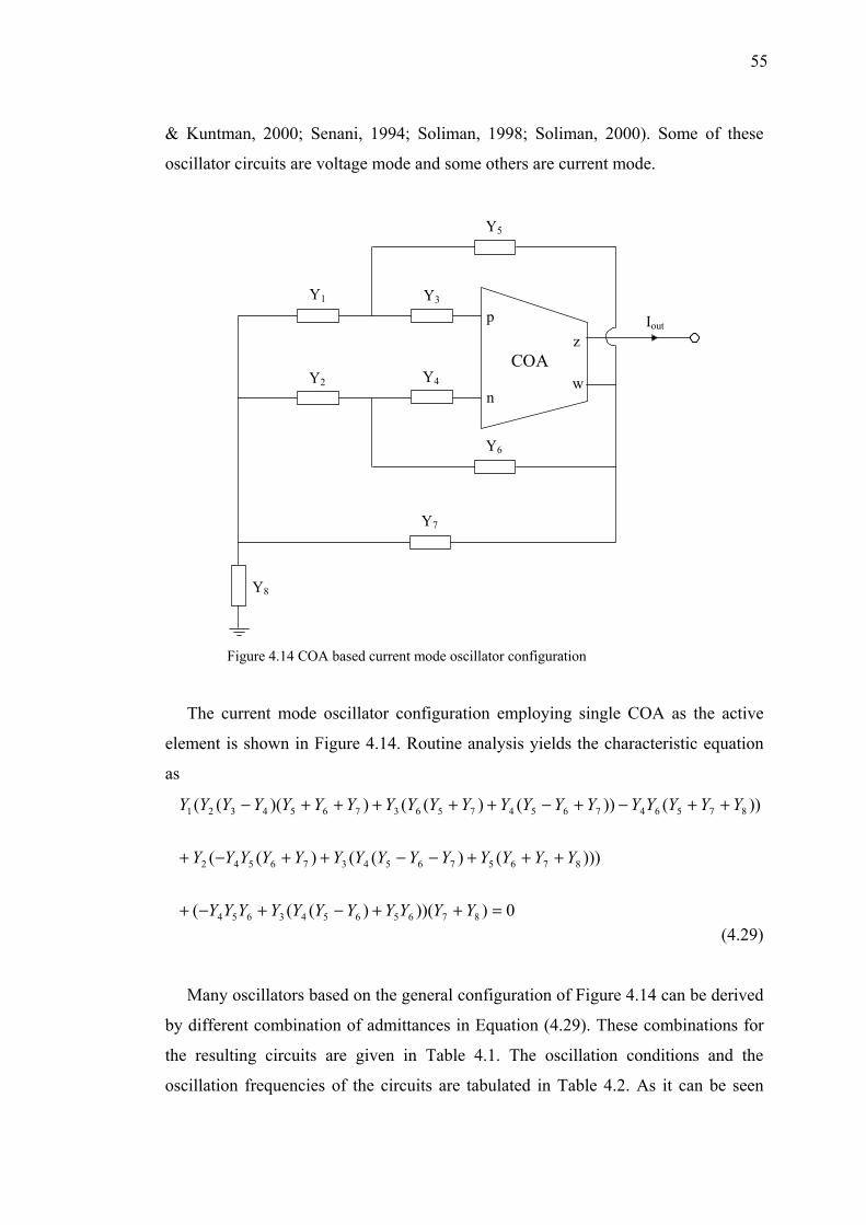
55
& Kuntman, 2000; Senani, 1994; Soliman, 1998; Soliman, 2000). Some of these
oscillator circuits are voltage mode and some others are current mode.
Y1
Y2 Y4
Y5
Y3
Y8
Y6
Y7
p
n
z
wCOA
Iout
Figure 4.14 COA based current mode oscillator configuration
The current mode oscillator configuration employing single COA as the active
element is shown in Figure 4.14. Routine analysis yields the characteristic equation
as
0)))()(((
)))()(()((
))())()(())(((
87656543654
87657654376542
87564765475637654321
=++−+−+
+++−−++−+
++−+−+++++−
YYYYYYYYYYY
YYYYYYYYYYYYYY
YYYYYYYYYYYYYYYYYYYY
(4.29)
Many oscillators based on the general configuration of Figure 4.14 can be derived
by different combination of admittances in Equation (4.29). These combinations for
the resulting circuits are given in Table 4.1. The oscillation conditions and the
oscillation frequencies of the circuits are tabulated in Table 4.2. As it can be seen
56
from Tables 4.1 and 4.2, the first four circuits are single frequency oscillators
containing only two capacitors and two resistors. The oscillation frequency of the
fifth circuit can independently be adjusted by a grounded resistor without affecting
the oscillation condition. If we interchange each capacitor with a resistor and each
resistor with a capacitor in oscillator-5, the resulting circuit is still a single resistance
controlled oscillator in the expense of using one more capacitor that violates the
canonic realization. With the last five circuits in Tables 4.1 and 4.2, it is possible to
achieve independent control on the oscillation condition without affecting the
oscillation frequency. All of the tabulated circuits employ only two dynamical
elements meaning that the presented oscillators are canonic. The single frequency
oscillators utilize two resistors. The remaining six circuits use three resistors for
independent control of the oscillation frequency or the oscillation condition. In this
respect, they contain minimum number of passive elements.
It can easily be shown that all the passive sensitivities of the oscillation
frequencies of circuits except for oscillator-5 are one half in magnitude. For the fifth
circuit sensitivities are
83
8
83
3
21
21
21
0
8
0
3
0
7
0
2
0
6
GGG
S
GGG
S
SSS
G
G
CCG
+=
+=
=−=−=
ω
ω
ωωω
(4.30)
which are not more than one half in magnitude.
To verify the theoretical study, the oscillator circuits have been simulated using
PSPICE program. As an illustrating example the simulation result of the current
mode single resistance controlled oscillator is given. For this circuit passive
components are chosen as R3=R8=1kΩ, R6=2kΩ, C2=C7=100pF, which result in
1.59MHz oscillation frequency. The PSPICE simulations were performed using the
CMOS realizations of COA given in Figure 3.7.
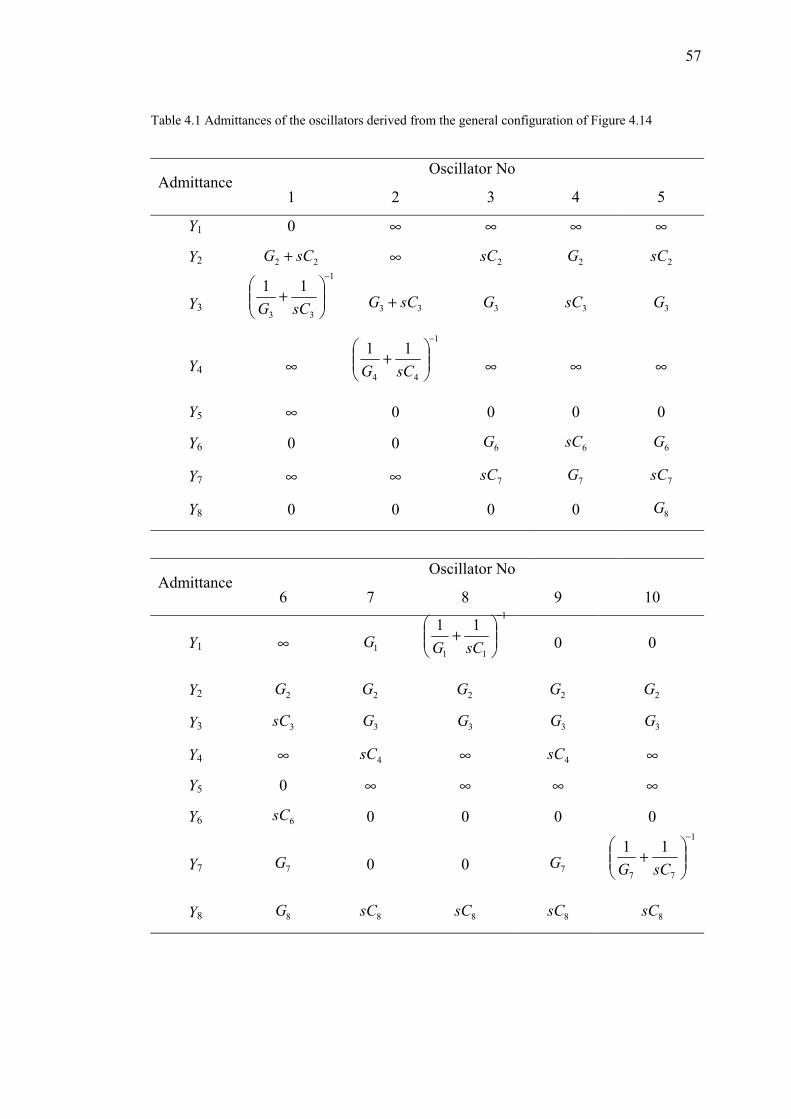
57
Table 4.1 Admittances of the oscillators derived from the general configuration of Figure 4.14
Oscillator No Admittance
1 2 3 4 5
Y1 0 ∞ ∞ ∞ ∞
Y2 22 sCG + ∞ 2sC 2G 2sC
Y3
1
33
11−
+
sCG 33 sCG + 3G 3sC 3G
Y4 ∞
1
44
11−
+
sCG ∞ ∞ ∞
Y5 ∞ 0 0 0 0
Y6 0 0 6G 6sC 6G
Y7 ∞ ∞ 7sC 7G 7sC
Y8 0 0 0 0 8G
Oscillator No Admittance
6 7 8 9 10
Y1 ∞ 1G
1
11
11−
+
sCG 0 0
Y2 2G 2G 2G 2G 2G
Y3 3sC 3G 3G 3G 3G
Y4 ∞ 4sC ∞ 4sC ∞
Y5 0 ∞ ∞ ∞ ∞
Y6 6sC 0 0 0 0
Y7 7G 0 0 7G
1
77
11−
+
sCG
Y8 8G 8sC 8sC 8sC 8sC
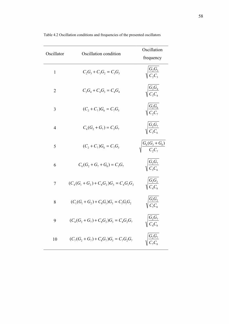
58
Table 4.2 Oscillation conditions and frequencies of the presented oscillators
Oscillator Oscillation condition Oscillation
frequency
1 332332 GCGCGC =+ 32
32
CCGG
2 443443 GCGCGC =+ 43
43
CCGG
3 37672 )( GCGCC =+ 72
63
CCGG
4 73726 )( GCGGC =+ 63
72
CCGG
5 37672 )( GCGCC =+ 72
836 )(CC
GGG +
6 738726 )( GCGGGC =++ 63
72
CCGG
7 214328214 ))(( GGCGGCGGC =++84
21
CCGG
8 211318211 ))(( GGCGGCGGC =++ 81
21
CCGG
9 724328724 ))(( GGCGGCGGC =++ 84
72
CCGG
10 727378727 ))(( GGCGGCGGC =++ 87
72
CCGG
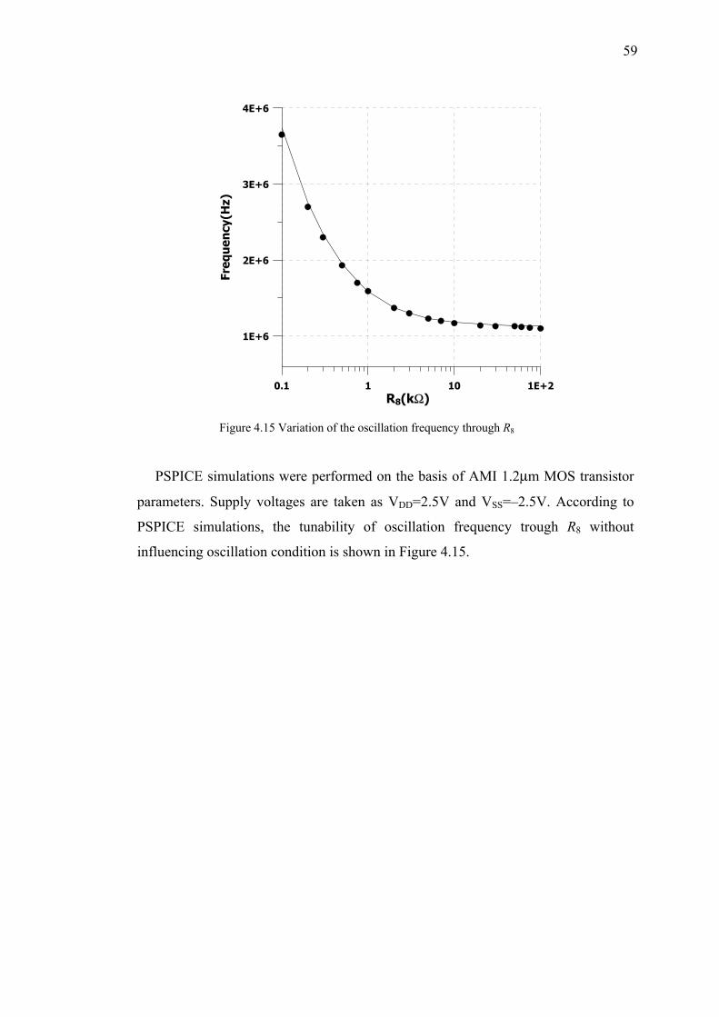
59
0.1 1 10 1E+2R3(K)
1E+6
2E+6
3E+6
4E+6
Freq
uenc
y(H
z)
R8(kΩ) Figure 4.15 Variation of the oscillation frequency through R8
PSPICE simulations were performed on the basis of AMI 1.2µm MOS transistor
parameters. Supply voltages are taken as VDD=2.5V and VSS=–2.5V. According to
PSPICE simulations, the tunability of oscillation frequency trough R8 without
influencing oscillation condition is shown in Figure 4.15.
CHAPTER FIVE
ANALOG CIRCUIT DESIGN USING OTRA
This Chapter presents new high performance circuit topologies that employ
OTRA to be used in analog systems. They constitute alternative candidates to the
existing circuits, which use other active elements, especially the op-amp. The
presented circuits can be grouped as analog filters, sinusoidal oscillators and
immitance simulators. The filter configurations make it possible to realize first order
allpass filter and biquads with all five different filtering functions. High order and
multifunction filters can also be synthesized using another presented topology.
Transimpedance type universal filter configuration is included too. They all enjoy the
advantageous properties of the OTRA presented in Chapter 2.
5.1 Allpass and Notch Filters
As mentioned in Chapter 4, allpass filters are important parts of many circuits and
systems. They are generally used for introducing a frequency dependent delay while
keeping the amplitude of the input signal constant over the desired frequency range.
Other types of active circuits such as quadrature oscillators and high Q bandpass
filters are also realized by using allpass filters (Comer et al., 1997; Çam, Çiçekoğlu
et al., 2000; Çiçekoğlu, Kuntman & Berk, 1999; Higashimura & Fukiu, 1988;
Schauman & Van Valkenburg, 2001; Toker et al., 2000). Op-amp, current conveyor
and four terminal floating nullor based first order allpass filters are available in the
literature (Comer et al., 1997; Çam, Çiçekoğlu et al., 2000; Çiçekoğlu et al., 1999).
In Comer et al. (1997) a voltage mode allpass filter has been presented which
contains an op-amp, three resistors and a capacitor. A set of current conveyor based
first order allpass filter sections have been presented in the literature (Çiçekoğlu et
al., 1999). The voltage mode allpass filter contains single four terminal floating
nullor, a capacitor and two grounded resistors in Çam, Çiçekoğlu et al. (2000). Most
of them can either realize first order or second order allpass filters.
60
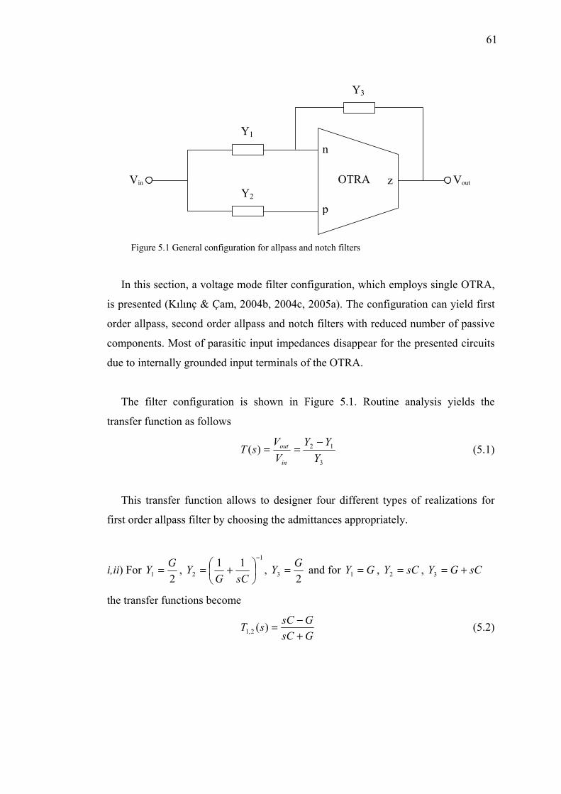
61
Vin
n
p
zOTRA Vout
Y1
Y2
Y3
Figure 5.1 General configuration for allpass and notch filters
In this section, a voltage mode filter configuration, which employs single OTRA,
is presented (Kılınç & Çam, 2004b, 2004c, 2005a). The configuration can yield first
order allpass, second order allpass and notch filters with reduced number of passive
components. Most of parasitic input impedances disappear for the presented circuits
due to internally grounded input terminals of the OTRA.
The filter configuration is shown in Figure 5.1. Routine analysis yields the
transfer function as follows
3
12)(Y
YYVV
sTin
out −== (5.1)
This transfer function allows to designer four different types of realizations for
first order allpass filter by choosing the admittances appropriately.
i,ii) For 21G=Y ,
1
211 −
+=
sCGY ,
23G=Y and for Y , Y , Y
the transfer functions become
G=1 sC=2 sCG +=3
GsCGsCsT
+−=)(2,1 (5.2)

62
iii,iv) For 1
111 −
+=
sCGY ,
22G=Y ,
23G=Y and for Y , , Y
the transfer functions become
sC=1 GY =2 sCG +=3
GsCGsCsT
+−−=)(4,3 (5.3)
Thus, both inverting and non-inverting types of first order allpass filters are
realized. The allpass filters have the following phase responses
−=
−°=
GCnarcta
GCnarcta
ωωϕ
ωωϕ
2)(
2180)(
4,3
2,1
(5.4)
It is also possible to obtain second order allpass and notch filters from the
configuration of Figure 5.1. For 1
111
11−
+=
sCGY , the transfer
function becomes
2232 sCGYY +==
211221212
21111221212
5 )()()(
GGGCGCsCCsGGGCGCGCsCCssT
++++−++
= (5.5)
It results a second order allpass and notch responses if the conditions
and C are satisfied, respectively. The
resonant frequency and the quality factor of these filters are expressed as
111221 )(2 GCGCGC =+ 111221 GCGCG =+
21
210 CC
GG=ω (5.6)
11
22
1221
2121
GCGCk
GCGCGGCC
Q =+
= (5.7)
where k=1 for notch filter and k=2 for allpass filter. It is possible to tune the resonant
frequency (ω0) and the quality factor (Q) orthogonally. One filter parameter can be
adjusted by suitably changing the component values provided that the ratio in the
equation of the other filter parameter is kept constant. By this way, the other filter
63
parameter will not be altered. For instance, if we want to change Q without
disturbing ω0, G1G2/C1C2 ratio should be kept constant. For this purpose, we can
change Q by multiplying C1 and G1 (or C2 and G2) by the same factor. This does not
alter the value of ω0. One can also tune ω0 without disturbing the Q value using the
same way.
Sensitivity analysis of the second order allpass and notch filters with respect to
passive elements yields
1221
21
1221
12
21
21
21
12
21
0
2
0
1
0
2
0
1
GCGCGCSS
GCGCGC
SS
SSSS
QC
QG
QC
QG
CCGG
+−==
+−==
=−=−== ωωωω
(5.8)
It is clearly observed from Equation (5.8) that all passive sensitivities are no more
than one half in magnitude for the presented second order allpass and notch filters.
The effects of the major non-idealities inherent in the OTRA on the presented
filters are considered and self compensation introduced by Salama & Soliman
(1999b) is employed for high frequencies. Considering a single pole model for the
transresistance gain, Rm, then
0
0
1)(
ωs
RsRm
+= (5.9)
For filter applications which are intended for high frequencies, the transresistance
gain, Rm(s), reduces to
pm sC
sR 1)( ≈ (5.10)
where
64
00
1ωR
C p = (5.11)
Taking into account this effect the transfer function in Equation (5.1) becomes
psCYYYsT
+−
=3
12)( (5.12)
For complete compensation, the admittance Y3 must contain capacitor branch. In
that case the filters can be designed taking the magnitude of Cp into consideration, by
subtracting its magnitude from the capacitance value in Y3. Thus the effect of Cp can
be absorbed in the integrating capacitance without using any additional elements and
achieving complete self compensation (Salama & Soliman, 1999b). The concept of
self compensation is applicable to the transfer functions T2, T4 and T5 which all
contain capacitor elements in the admittance Y3. For the other two presented circuits,
transfer functions become
++−=−=
sGCGsCGsCsTsT
p )2(11)()( 31 (5.13)
If the value of Cp is low enough and if we choose the value of G high enough,
then the above non-ideal response would approach to the ideal first order allpass
response.
To verify the theoretical study, the first order allpass filter, which corresponds to
the transfer function T1,2, was constructed and simulated with PSPICE program. For
this purpose, passive components were chosen as R=1kΩ and C=1nF which results
in 159kHz center frequency. The PSPICE simulations were performed by using a
CMOS realization of OTRA (Salama & Soliman, 1999a) given in Figure 3.8.
PSPICE simulations were performed by AMI 1.2µm MOS transistor parameters with
the same aspect ratios as in Salama & Soliman (1999a). Supply voltages are taken as
VDD=2.5V and VSS=−2.5V. Simulated magnitude and phase responses of the first
order allpass filter are given in Figures 5.2 and 5.3, respectively. The deviations in
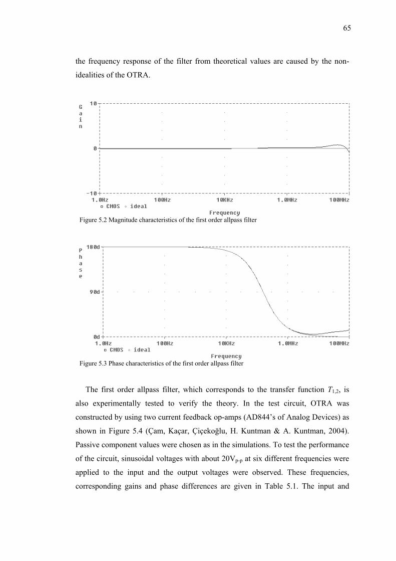
65
the frequency response of the filter from theoretical values are caused by the non-
idealities of the OTRA.
Figure 5.2 Magnitude characteristics of the first order allpass filter
Figure 5.3 Phase characteristics of the first order allpass filter
The first order allpass filter, which corresponds to the transfer function T1,2, is
also experimentally tested to verify the theory. In the test circuit, OTRA was
constructed by using two current feedback op-amps (AD844’s of Analog Devices) as
shown in Figure 5.4 (Çam, Kaçar, Çiçekoğlu, H. Kuntman & A. Kuntman, 2004).
Passive component values were chosen as in the simulations. To test the performance
of the circuit, sinusoidal voltages with about 20Vp-p at six different frequencies were
applied to the input and the output voltages were observed. These frequencies,
corresponding gains and phase differences are given in Table 5.1. The input and
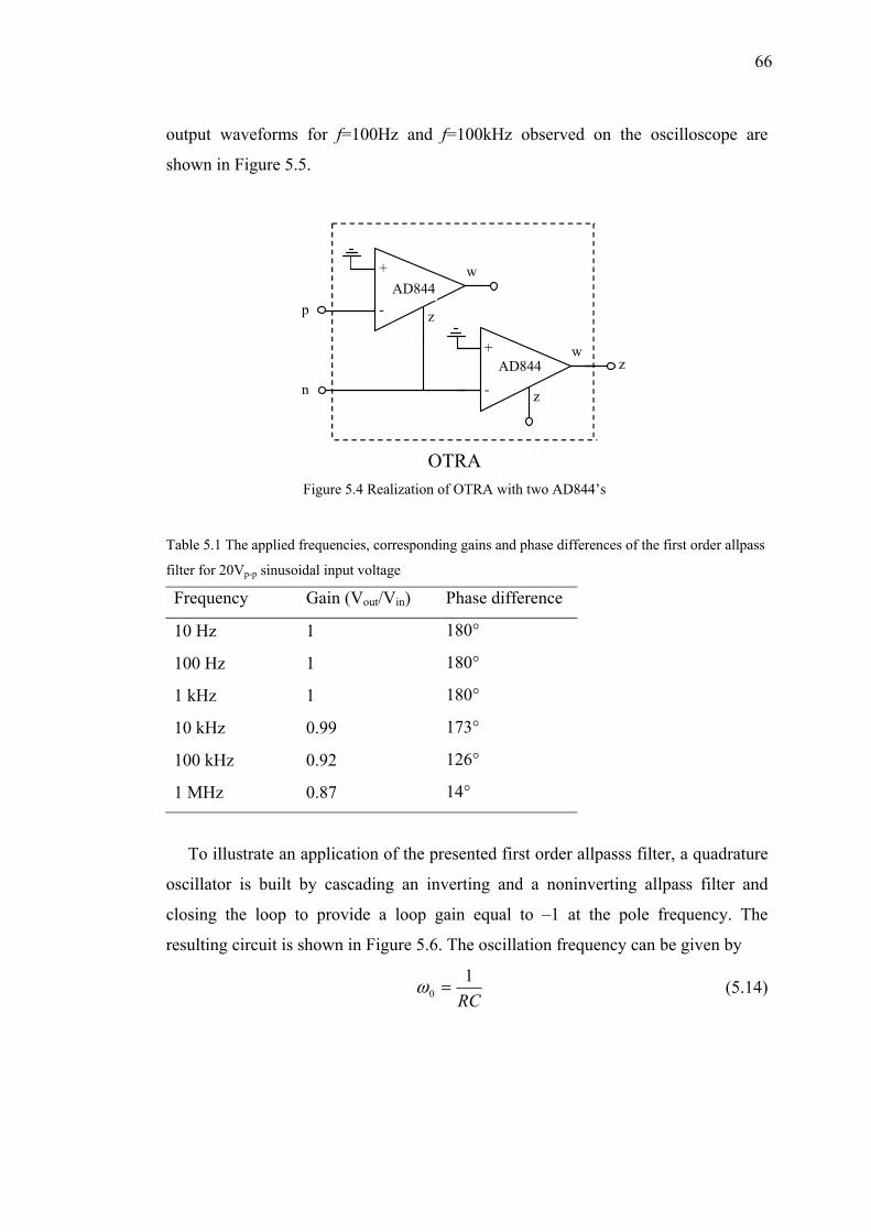
66
output waveforms for f=100Hz and f=100kHz observed on the oscilloscope are
shown in Figure 5.5.
+
- z
w
+
- z
w
n
p
z
OTRA
AD844
AD844
Figure 5.4 Realization of OTRA with two AD844’s
Table 5.1 The applied frequencies, corresponding gains and phase differences of the first order allpass
filter for 20Vp-p sinusoidal input voltage
Frequency Gain (Vout/Vin) Phase difference
10 Hz 1 180°
100 Hz 1 180°
1 kHz 1 180°
10 kHz 0.99 173°
100 kHz 0.92 126°
1 MHz 0.87 14°
To illustrate an application of the presented first order allpasss filter, a quadrature
oscillator is built by cascading an inverting and a noninverting allpass filter and
closing the loop to provide a loop gain equal to –1 at the pole frequency. The
resulting circuit is shown in Figure 5.6. The oscillation frequency can be given by
RC1
0 =ω (5.14)
67
(a)
(b)
Figure 5.5 Experimental waveforms (a) at f=100 Hz and (b) at f=100 kHz; Volt/Div=2V
By choosing R=1kΩ and C=1nF, the calculated value of the oscillation frequency
is found as f0=159kHz which is in close agreement with the simulated result. The
simulated waveforms of the oscillator are shown in Figure 5.7. The frequency
spectrum of oscillated waveform in the quadrature oscillator is depicted in Figure
5.8. Total harmonic distortion for the voltages V1 and V2 are 0.32% and 0.47%
respectively.
68
n
p
zOTRA V2
2R
C R
2R
n
p
z OTRA
2R
CR
2R
V1
Figure 5.6 An application example of quadrature oscillator constructed by two allpass filters
Figure 5.7 Output waveforms of the first order allpass filter based quadrature oscillator
200 600 1000 14000 400 800 1200Frequency (kHz)
(dB)
-10
-30
-50
-70
-90
Figure 5.8 The frequency spectrum of V1
69
5.2 Lowpass, Highpass and Bandpass Biquads
As mentioned before, active filters employing a single active element are
especially useful for applications where the power consumption is an important
design constraint. Several voltage mode filters that use a single active element rather
than the op-amp have been developed (Horng, Lay, Chang & Lee, 1997; Liu & Lee,
1996; Liu & Lee, 1997; Liu & Tsao, 1991; Liu, Chen, Tsao & Tsay, 1993) to
overcome well known op-amp limitations such as constant gain-bandwidth product,
low slew rate, etc. Some of these filters use more than one active element (Horng et
al., 1997; Liu & Lee, 1996; Liu & Lee, 1997). Some others (Liu & Tsao, 1991; Liu et
al., 1993) employ a single current follower or a single current conveyor which are
unity gain active elements.
The main objective of this section is to present single OTRA based lowpass,
highpass and bandpass biquads (Kılınç & Çam, 2003g, 2003h) taking advantages of
OTRA, especially the very large transresistance gain, that provide further
possibilities for the designers in the realization of analog signal processing circuits.
The filters are insensitive to stray capacitances and parasitic resistances due to
internally grounded input terminals of OTRA.
Vin
n
p
zOTRA Vout
Y1
Y2 Y3
Y4
Y5
Figure 5.9 General configuration for the single OTRA biquad
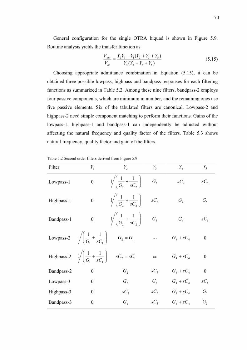
70
General configuration for the single OTRA biquad is shown in Figure 5.9.
Routine analysis yields the transfer function as
)()(
5324
532132
YYYYYYYYYY
VV
in
out
++++−
= (5.15)
Choosing appropriate admittance combination in Equation (5.15), it can be
obtained three possible lowpass, highpass and bandpass responses for each filtering
functions as summarized in Table 5.2. Among these nine filters, bandpass-2 employs
four passive components, which are minimum in number, and the remaining ones use
five passive elements. Six of the tabulated filters are canonical. Lowpass-2 and
highpass-2 need simple component matching to perform their functions. Gains of the
lowpass-1, highpass-1 and bandpass-1 can independently be adjusted without
affecting the natural frequency and quality factor of the filters. Table 5.3 shows
natural frequency, quality factor and gain of the filters.
Table 5.2 Second order filters derived from Figure 5.9
Filter 1Y 2Y 3Y 4Y 5Y
Lowpass-1 0
+
22
111sCG 3G 4sC 5sC
Highpass-1 0
+
22
111sCG 3sC 4G 5G
Bandpass-1 0
+
22
111sCG 3G 4G 5sC
Lowpass-2
+
11
111sCG 12 GG = ∞ 44 sCG + 0
Highpass-2
+
11
111sCG 12 sCsC = ∞ 44 sCG + 0
Bandpass-2 0 2G 3sC 44 sCG + 0
Lowpass-3 0 2G 3G 44 sCG + 5sC
Highpass-3 0 2sC 3sC 44 sCG + 5G
Bandpass-3 0 2G 3sC 44 sCG + 5G
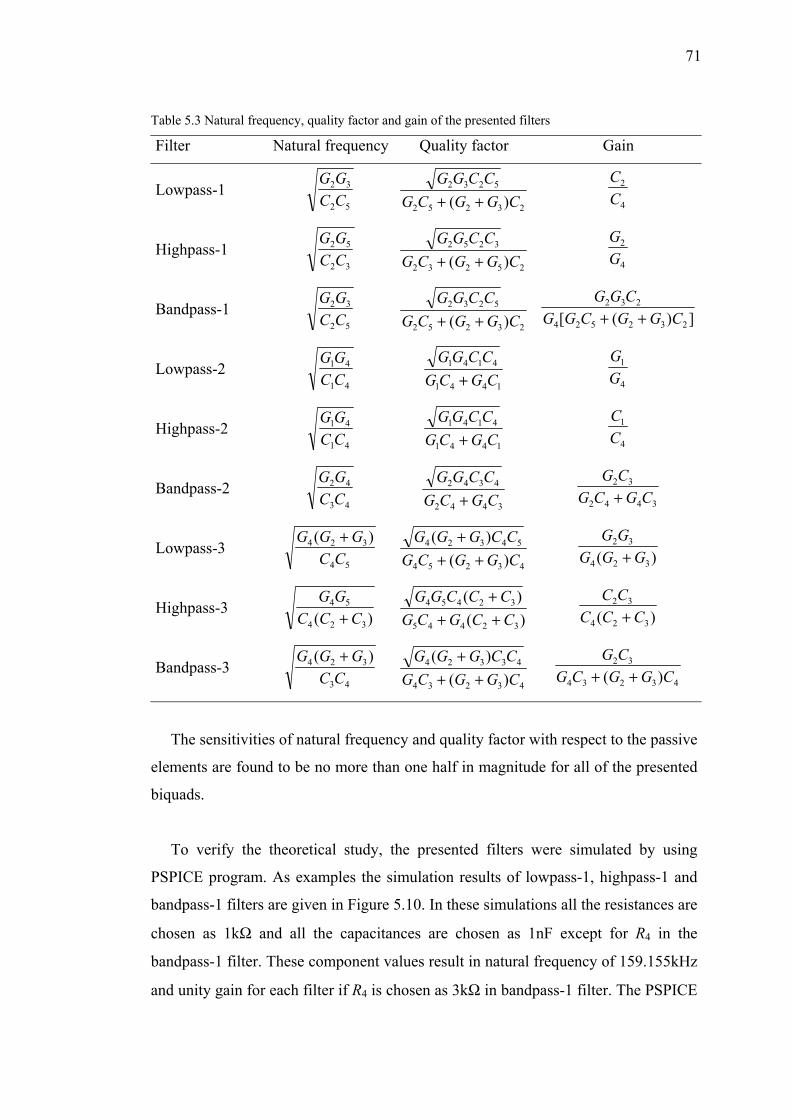
71
Table 5.3 Natural frequency, quality factor and gain of the presented filters
Filter Natural frequency Quality factor Gain
Lowpass-1 52
32
CCGG
23252
5232
)( CGGCGCCGG
++ 4
2
CC
Highpass-1 32
52
CCGG
25232
3252
)( CGGCGCCGG
++ 4
2
GG
Bandpass-1 52
32
CCGG
23252
5232
)( CGGCGCCGG
++ ])([ 232524
232
CGGCGGCGG++
Lowpass-2 41
41
CCGG
1441
4141
CGCGCCGG
+
4
1
GG
Highpass-2 41
41
CCGG
1441
4141
CGCGCCGG
+
4
1
CC
Bandpass-2 43
42
CCGG
3442
4342
CGCGCCGG
+
3442
32
CGCGCG+
Lowpass-3 54
324 )(CC
GGG + 43254
54324
)()(
CGGCGCCGGG
+++
)( 324
32
GGGGG+
Highpass-3 )( 324
54
CCCGG+
)()(
32445
32454
CCGCGCCCGG+++
)( 324
32
CCCCC+
Bandpass-3 43
324 )(CC
GGG + 43234
43324
)()(
CGGCGCCGGG
+++
43234
32
)( CGGCGCG++
The sensitivities of natural frequency and quality factor with respect to the passive
elements are found to be no more than one half in magnitude for all of the presented
biquads.
To verify the theoretical study, the presented filters were simulated by using
PSPICE program. As examples the simulation results of lowpass-1, highpass-1 and
bandpass-1 filters are given in Figure 5.10. In these simulations all the resistances are
chosen as 1kΩ and all the capacitances are chosen as 1nF except for R4 in the
bandpass-1 filter. These component values result in natural frequency of 159.155kHz
and unity gain for each filter if R4 is chosen as 3kΩ in bandpass-1 filter. The PSPICE
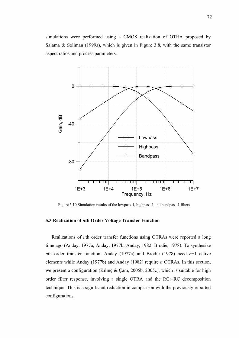
72
simulations were performed using a CMOS realization of OTRA proposed by
Salama & Soliman (1999a), which is given in Figure 3.8, with the same transistor
aspect ratios and process parameters.
1E+3 1E+4 1E+5 1E+6 1E+7Frequency, Hz
-80
-40
0
Gai
n, d
B
Lowpass
Highpass
Bandpass
Figure 5.10 Simulation results of the lowpass-1, highpass-1 and bandpass-1 filters
5.3 Realization of nth Order Voltage Transfer Function
Realizations of nth order transfer functions using OTRAs were reported a long
time ago (Anday, 1977a; Anday, 1977b; Anday, 1982; Brodie, 1978). To synthesize
nth order transfer function, Anday (1977a) and Brodie (1978) need n+1 active
elements while Anday (1977b) and Anday (1982) require n OTRAs. In this section,
we present a configuration (Kılınç & Çam, 2005b, 2005c), which is suitable for high
order filter response, involving a single OTRA and the RC:−RC decomposition
technique. This is a significant reduction in comparison with the previously reported
configurations.
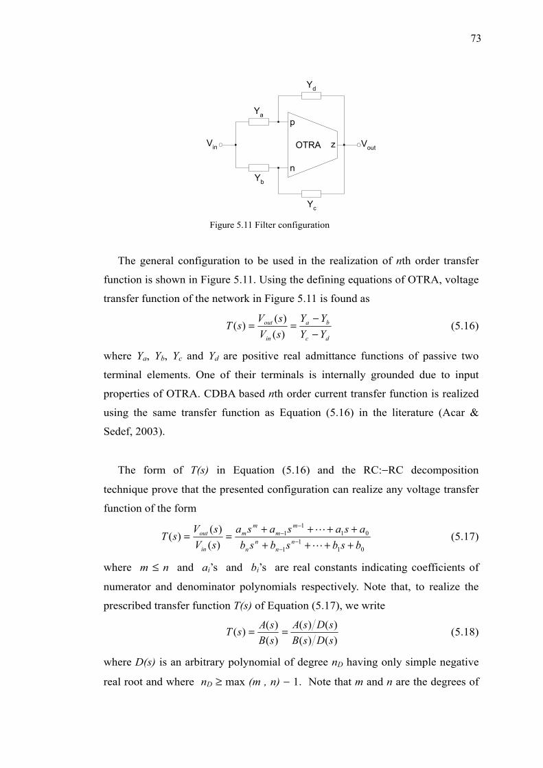
73
p
n
zOTRAVin Vout
Ya
Yb
Yd
Yc Figure 5.11 Filter configuration
The general configuration to be used in the realization of nth order transfer
function is shown in Figure 5.11. Using the defining equations of OTRA, voltage
transfer function of the network in Figure 5.11 is found as
dc
ba
in
out
YYYY
sVsV
sT−−
==)()(
)( (5.16)
where Ya, Yb, Yc and Yd are positive real admittance functions of passive two
terminal elements. One of their terminals is internally grounded due to input
properties of OTRA. CDBA based nth order current transfer function is realized
using the same transfer function as Equation (5.16) in the literature (Acar &
Sedef, 2003).
The form of T(s) in Equation (5.16) and the RC:−RC decomposition
technique prove that the presented configuration can realize any voltage transfer
function of the form
011
1
011
1
)()(
)(bsbsbsbasasasa
sVsV
sT nn
nn
mm
mm
in
out
++++++++
== −−
−−
L
L (5.17)
where m ≤ n and ai’s and bi’s are real constants indicating coefficients of
numerator and denominator polynomials respectively. Note that, to realize the
prescribed transfer function T(s) of Equation (5.17), we write
)()()()(
)()()(
sDsBsDsA
sBsAsT == (5.18)
where D(s) is an arbitrary polynomial of degree nD having only simple negative
real root and where nD ≥ max (m , n) − 1. Note that m and n are the degrees of
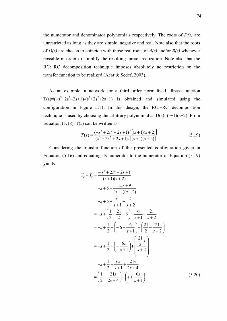
74
the numerator and denominator polynomials respectively. The roots of D(s) are
unrestricted as long as they are simple, negative and real. Note also that the roots
of D(s) are chosen to coincide with those real roots of A(s) and/or B(s) whenever
possible in order to simplify the resulting circuit realization. Note also that the
RC:−RC decomposition technique imposes absolutely no restriction on the
transfer function to be realized (Acar & Sedef, 2003).
As an example, a network for a third order normalized allpass function
T(s)=(−s3+2s2−2s+1)/(s3+2s2+2s+1) is obtained and simulated using the
configuration in Figure 5.11. In this design, the RC:−RC decomposition
technique is used by choosing the arbitrary polynomial as D(s)=(s+1)(s+2). From
Equation (5.18), T(s) can be written as
[ ][ ])2)(1()122(
)2)(1()122()( 23
23
++++++++−+−=
sssssssssssT (5.19)
Considering the transfer function of the presented configuration given in
Equation (5.16) and equating its numerator to the numerator of Equation (5.19)
yields
++−
++=
++
+−+−=
++
+−++−=
+−+
++−++−=
+−
++
−++−=
+−
+++−=
+++−+−=
+++−+−=−
16
4221
21
4221
16
21
2221
16
21
221
221
166
21
221
166
221
21
221
165
)2)(1(9155
)2)(1(122 23
sss
ss
ss
sss
s
s
sss
sss
sss
sss
ssss
sssssYY ba
(5.20)
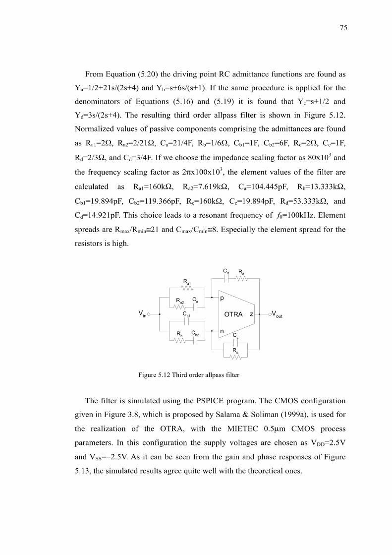
75
From Equation (5.20) the driving point RC admittance functions are found as
Ya=1/2+21s/(2s+4) and Yb=s+6s/(s+1). If the same procedure is applied for the
denominators of Equations (5.16) and (5.19) it is found that Yc=s+1/2 and
Yd=3s/(2s+4). The resulting third order allpass filter is shown in Figure 5.12.
Normalized values of passive components comprising the admittances are found
as Ra1=2Ω, Ra2=2/21Ω, Ca=21/4F, Rb=1/6Ω, Cb1=1F, Cb2=6F, Rc=2Ω, Cc=1F,
Rd=2/3Ω, and Cd=3/4F. If we choose the impedance scaling factor as 80x103 and
the frequency scaling factor as 2πx100x103, the element values of the filter are
calculated as Ra1=160kΩ, Ra2=7.619kΩ, Ca=104.445pF, Rb=13.333kΩ,
Cb1=19.894pF, Cb2=119.366pF, Rc=160kΩ, Cc=19.894pF, Rd=53.333kΩ, and
Cd=14.921pF. This choice leads to a resonant frequency of f0=100kHz. Element
spreads are Rmax/Rmin≅21 and Cmax/Cmin≅8. Especially the element spread for the
resistors is high.
p
n
zOTRAVin Vout
Ra2
Ra1
Ca
RbCb2
Cb1
RdCd
Rc
Cc
Figure 5.12 Third order allpass filter
The filter is simulated using the PSPICE program. The CMOS configuration
given in Figure 3.8, which is proposed by Salama & Soliman (1999a), is used for
the realization of the OTRA, with the MIETEC 0.5µm CMOS process
parameters. In this configuration the supply voltages are chosen as VDD=2.5V
and VSS=−2.5V. As it can be seen from the gain and phase responses of Figure
5.13, the simulated results agree quite well with the theoretical ones.
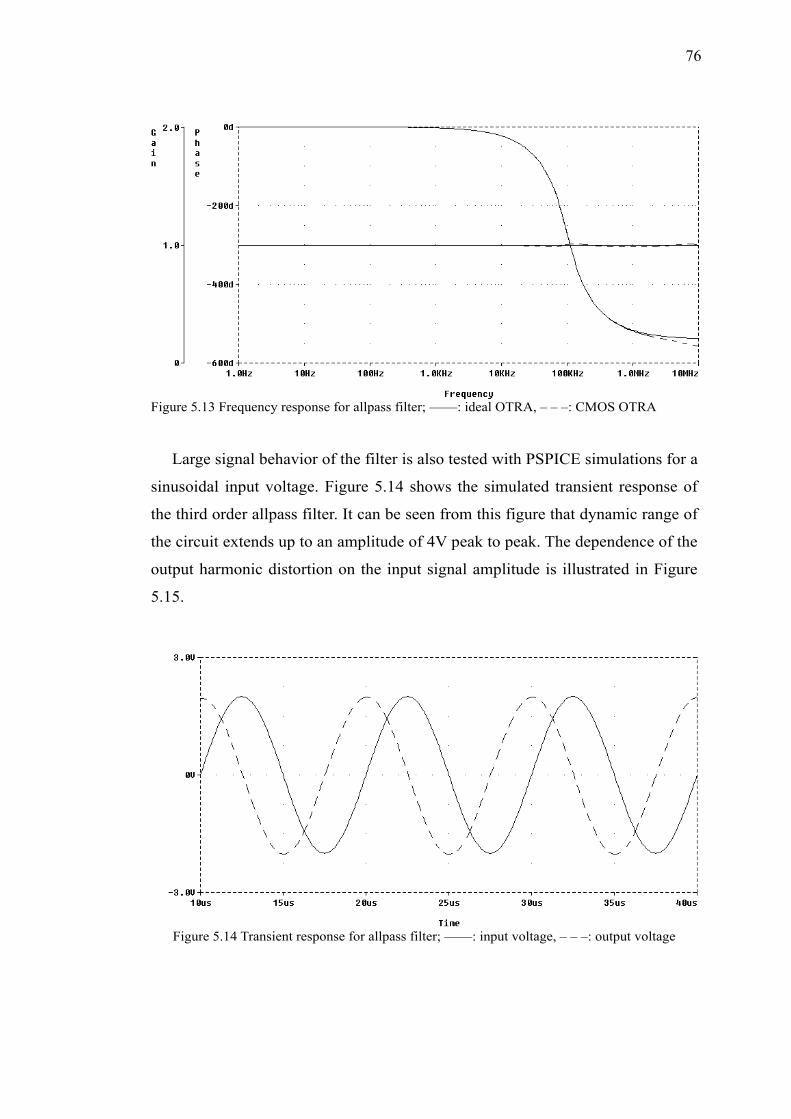
76
Figure 5.13 Frequency response for allpass filter; ——: ideal OTRA, – – –: CMOS OTRA
Large signal behavior of the filter is also tested with PSPICE simulations for a
sinusoidal input voltage. Figure 5.14 shows the simulated transient response of
the third order allpass filter. It can be seen from this figure that dynamic range of
the circuit extends up to an amplitude of 4V peak to peak. The dependence of the
output harmonic distortion on the input signal amplitude is illustrated in Figure
5.15.
Figure 5.14 Transient response for allpass filter; ——: input voltage, – – –: output voltage
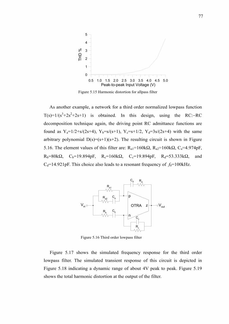
77
0.5 1.0 1.5 2.0 2.5 3.0 3.5 4.0 4.5 5.0Peak-to-peak Input Voltage (V)
0
1
2
3
4
5
THD
%
Figure 5.15 Harmonic distortion for allpass filter
As another example, a network for a third order normalized lowpass function
T(s)=1/(s3+2s2+2s+1) is obtained. In this design, using the RC:−RC
decomposition technique again, the driving point RC admittance functions are
found as Ya=1/2+s/(2s+4), Yb=s/(s+1), Yc=s+1/2, Yd=3s/(2s+4) with the same
arbitrary polynomial D(s)=(s+1)(s+2). The resulting circuit is shown in Figure
5.16. The element values of this filter are: Ra1=160kΩ, Ra2=160kΩ, Ca=4.974pF,
Rb=80kΩ, Cb=19.894pF, Rc=160kΩ, Cc=19.894pF, Rd=53.333kΩ, and
Cd=14.921pF. This choice also leads to a resonant frequency of f0=100kHz.
p
n
zOTRAVin Vout
Ra2
Ra1
Ca
RbCb
RdCd
Rc
Cc
Figure 5.16 Third order lowpass filter
Figure 5.17 shows the simulated frequency response for the third order
lowpass filter. The simulated transient response of this circuit is depicted in
Figure 5.18 indicating a dynamic range of about 4V peak to peak. Figure 5.19
shows the total harmonic distortion at the output of the filter.
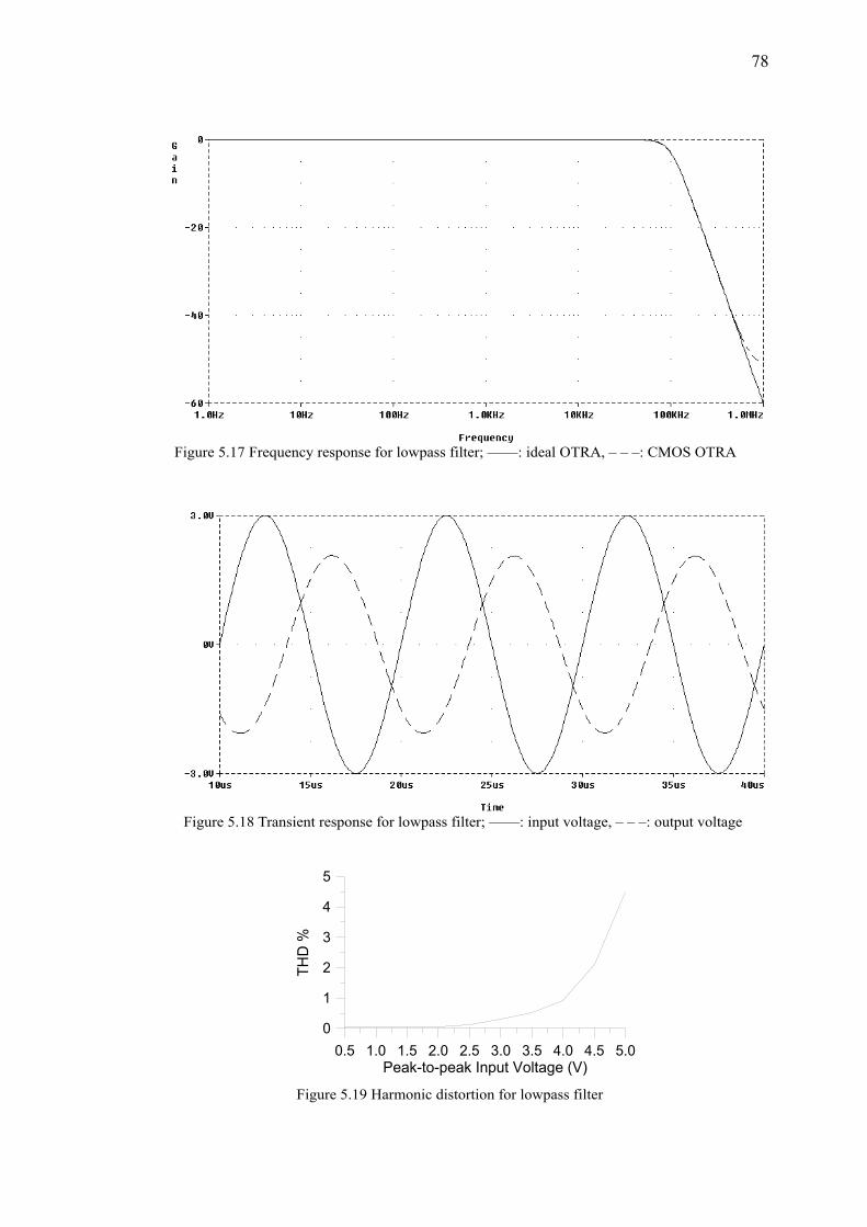
78
Figure 5.17 Frequency response for lowpass filter; ——: ideal OTRA, – – –: CMOS OTRA
Figure 5.18 Transient response for lowpass filter; ——: input voltage, – – –: output voltage
0.5 1.0 1.5 2.0 2.5 3.0 3.5 4.0 4.5 5.0Peak-to-peak Input Voltage (V)
0
1
2
3
4
5
THD
%
Figure 5.19 Harmonic distortion for lowpass filter
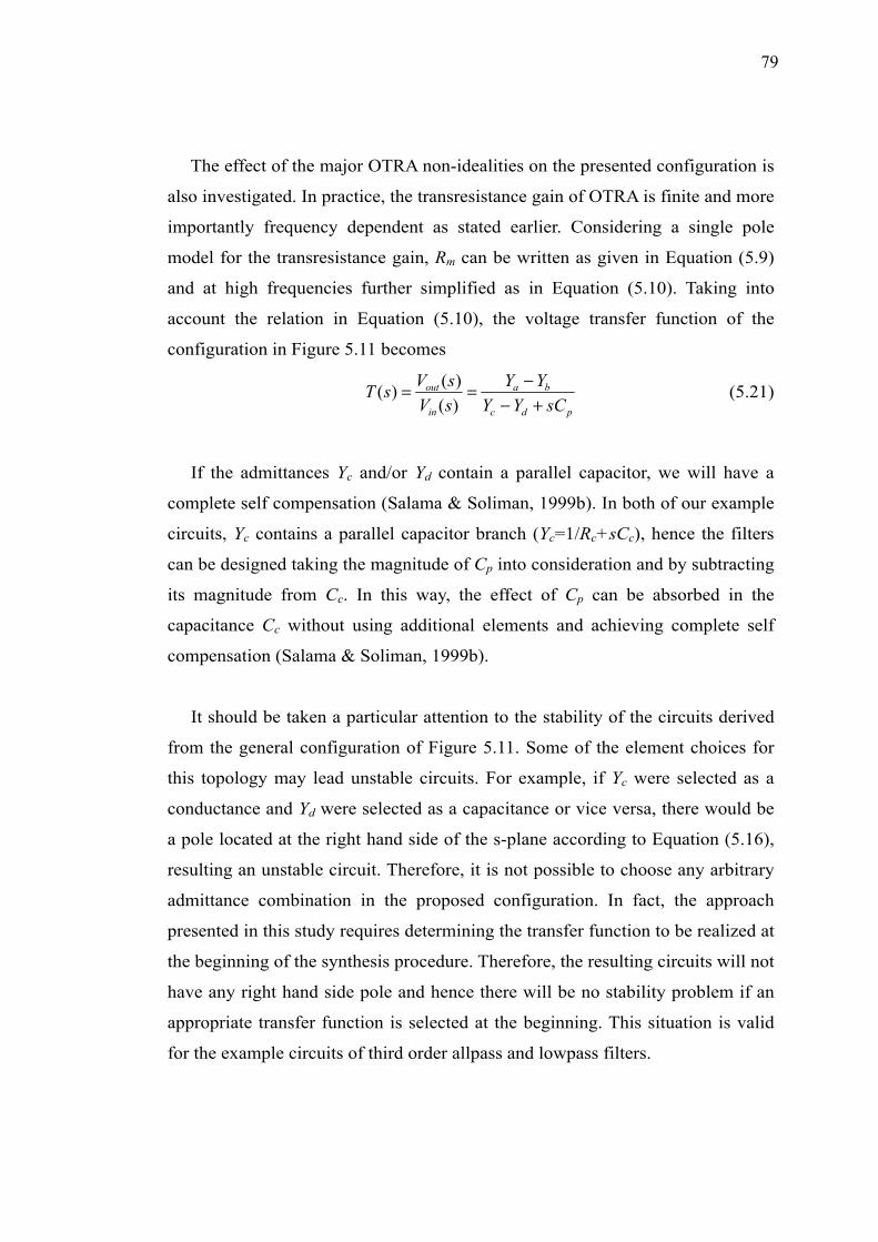
79
The effect of the major OTRA non-idealities on the presented configuration is
also investigated. In practice, the transresistance gain of OTRA is finite and more
importantly frequency dependent as stated earlier. Considering a single pole
model for the transresistance gain, Rm can be written as given in Equation (5.9)
and at high frequencies further simplified as in Equation (5.10). Taking into
account the relation in Equation (5.10), the voltage transfer function of the
configuration in Figure 5.11 becomes
pdc
ba
in
out
sCYYYY
sVsVsT
+−−==
)()()( (5.21)
If the admittances Yc and/or Yd contain a parallel capacitor, we will have a
complete self compensation (Salama & Soliman, 1999b). In both of our example
circuits, Yc contains a parallel capacitor branch (Yc=1/Rc+sCc), hence the filters
can be designed taking the magnitude of Cp into consideration and by subtracting
its magnitude from Cc. In this way, the effect of Cp can be absorbed in the
capacitance Cc without using additional elements and achieving complete self
compensation (Salama & Soliman, 1999b).
It should be taken a particular attention to the stability of the circuits derived
from the general configuration of Figure 5.11. Some of the element choices for
this topology may lead unstable circuits. For example, if Yc were selected as a
conductance and Yd were selected as a capacitance or vice versa, there would be
a pole located at the right hand side of the s-plane according to Equation (5.16),
resulting an unstable circuit. Therefore, it is not possible to choose any arbitrary
admittance combination in the proposed configuration. In fact, the approach
presented in this study requires determining the transfer function to be realized at
the beginning of the synthesis procedure. Therefore, the resulting circuits will not
have any right hand side pole and hence there will be no stability problem if an
appropriate transfer function is selected at the beginning. This situation is valid
for the example circuits of third order allpass and lowpass filters.
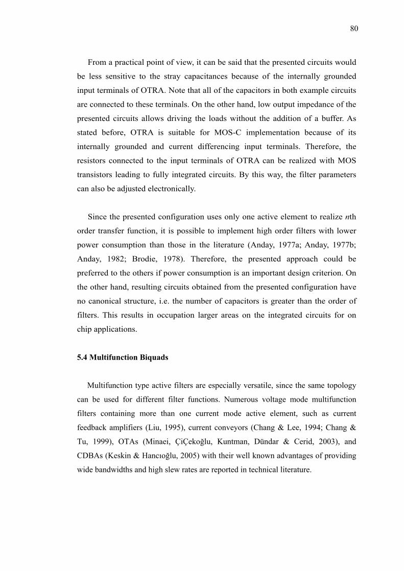
80
From a practical point of view, it can be said that the presented circuits would
be less sensitive to the stray capacitances because of the internally grounded
input terminals of OTRA. Note that all of the capacitors in both example circuits
are connected to these terminals. On the other hand, low output impedance of the
presented circuits allows driving the loads without the addition of a buffer. As
stated before, OTRA is suitable for MOS-C implementation because of its
internally grounded and current differencing input terminals. Therefore, the
resistors connected to the input terminals of OTRA can be realized with MOS
transistors leading to fully integrated circuits. By this way, the filter parameters
can also be adjusted electronically.
Since the presented configuration uses only one active element to realize nth
order transfer function, it is possible to implement high order filters with lower
power consumption than those in the literature (Anday, 1977a; Anday, 1977b;
Anday, 1982; Brodie, 1978). Therefore, the presented approach could be
preferred to the others if power consumption is an important design criterion. On
the other hand, resulting circuits obtained from the presented configuration have
no canonical structure, i.e. the number of capacitors is greater than the order of
filters. This results in occupation larger areas on the integrated circuits for on
chip applications.
5.4 Multifunction Biquads
Multifunction type active filters are especially versatile, since the same topology
can be used for different filter functions. Numerous voltage mode multifunction
filters containing more than one current mode active element, such as current
feedback amplifiers (Liu, 1995), current conveyors (Chang & Lee, 1994; Chang &
Tu, 1999), OTAs (Minaei, ÇiÇekoğlu, Kuntman, Dündar & Cerid, 2003), and
CDBAs (Keskin & Hancıoğlu, 2005) with their well known advantages of providing
wide bandwidths and high slew rates are reported in technical literature.

81
Although some OTRA based multifunction filters were described in the past
(Salama & Soliman, 1999a, 1999b), they all involve more than one OTRA. From the
point of view of power dissipation and manufacturing cost, it is advantageous to keep
the number of active elements at minimum.
In this section, a multi input, single output type voltage mode biquad, employing
single OTRA as the active element is presented, which realizes all of the five second
order filter functions, i.e., lowpass, highpass, bandpass, notch and allpass, without
changing the circuit topology.
Figure 5.20 Multifunction biquad
For the construction of OTRA based multifunction filter, let Ya be the admittance
between a voltage source Vin and positive input terminal, Yb the admittance between
Vin and negative input terminal, Yc the admittance between the output terminal z and
positive input terminal, and Yd admittance connecting negative input terminal to z
terminal of the OTRA. Voltage transfer function of this configuration can be
described by the following relationship.
cd
ba
in
z
YYYY
VV
−−
= (5.22)
If Ya=Ra||Ca , Zb=(1/Yb)=Rb+(1/sCb) , Zc=(1/Yc)=Rc+(1/sCc) , Yd=Rd||Cd and
splitting Ya - Yb junction into three parts as shown in Figure 5.20 and applying
82
superposition of input voltages Vin, V1, V2 in the circuit yields the equation for the
output voltage Vo (=Vz) as
ddccdcddcc
bbaain
abbbaa
d
a
bb
cc
cc
bbo
CRCRCRCRCRss
VCRCR
VCR
VCR
VCR
sVs
CC
CRCR
CRCRV
1111
1111
11
2
12122
+
−++
+
−++
⋅⋅++⋅=
(5.23)
In this equation, if we choose RbCb=RcCc it becomes
ddccdcddcc
bbaain
abbbaa
d
ao
CRCRCRCRCRss
VCRCR
VCR
VCR
VCR
sVs
CCV
1111
1111
2
12122
+
−++
+
−++
⋅= (5.24)
Lowpass, highpass, bandpass and bandstop responses can be obtained from
Equation (5.24) as will be described later.
Under Yc=0 selection, i.e. for Rc=∞ or Cc=0, Equation (5.23) reduces to
ddbbddbb
bbaain
abbbaa
d
ao
CRCRCRCRss
VCRCR
VCR
VCR
VCR
sVs
CCV
111
1111
2
12122
+
++
+
−++
⋅= (5.25)
Observe that the numerator of this equation is the same as Equation (5.24), but the
denominators differ. Equation (5.25) will be used to obtain allpass response.
With the circuit of Figure 5.20, all five different filter responses can be realized as
described below:
1. Lowpass; if V1 =Vin , V2=0, Ra=Rb in Equation (5.24)
2. Highpass; if V2 =Vin , V1=0, Ca=Cb in Equation (5.24)
3. Bandpass; if V1=V2=0 in Equation (5.24)
4. Bandstop; if V1=V2=Vin , RaCa=RdCd, RaCa+RbCb=RaCb in Equation (5.24)
5. Allpass; if V1=V2=Vin , RaCa=RdCd, 2(RaCa+RbCb)=RaCb in Equation (5.25)
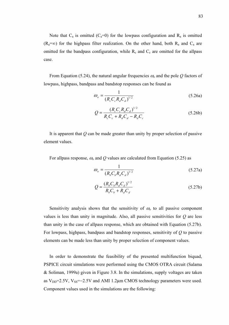
83
Note that Ca is omitted (Ca=0) for the lowpass configuration and Ra is omitted
(Ra=∞) for the highpass filter realization. On the other hand, both Ra and Ca are
omitted for the bandpass configuration, while Rc and Cc are omitted for the allpass
case.
From Equation (5.24), the natural angular frequencies ωo and the pole Q factors of
lowpass, highpass, bandpass and bandstop responses can be found as
2/1)(1
ddcco CRCR=ω (5.26a)
cdddcc
ddcc
CRCRCRCRCRQ−+
=2/1)(
(5.26b)
It is apparent that Q can be made greater than unity by proper selection of passive
element values.
For allpass response, ωo and Q values are calculated from Equation (5.25) as
2/1)(1
ddbbo CRCR=ω (5.27a)
ddbb
ddbb
CRCRCRCRQ
+=
2/1)( (5.27b)
Sensitivity analysis shows that the sensitivity of ωo to all passive component
values is less than unity in magnitude. Also, all passive sensitivities for Q are less
than unity in the case of allpass response, which are obtained with Equation (5.27b).
For lowpass, highpass, bandpass and bandstop responses, sensitivity of Q to passive
elements can be made less than unity by proper selection of component values.
In order to demonstrate the feasibility of the presented multifunction biquad,
PSPICE circuit simulations were performed using the CMOS OTRA circuit (Salama
& Soliman, 1999a) given in Figure 3.8. In the simulations, supply voltages are taken
as VDD=2.5V, VSS=−2.5V and AMI 1.2µm CMOS technology parameters were used.
Component values used in the simulations are the following:
84
a) Lowpass: Ra=Rb=Rc=Rd=100kΩ, Cb=Cc=10pF, Cd=20pF
b) Highpass: Rb=Rc=200kΩ, Rd=100kΩ, Ca=Cb=Cc=Cd=10pF
c) Bandpass: Rb=Rd=100kΩ, Rc=200kΩ, Cc=Cd=10pF, Cb=20pF
d) Bandstop: Ra=Rd=100kΩ, Rc=200kΩ, Ca=Cc=Cd=10pF, Rb=66.67kΩ, Cb=30pF
e) Allpass: Ra=Rd=400kΩ, Ca=Cd=10pF, Rb=100kΩ, Cb=40pF
All absolute ωo and Q component sensitivities at the above given values are less
than or equal to unity. The simulation results are depicted in Figure 5.21.
Figure 5.21 Simulation results for five different filter transfer functions
5.5 Transimpedance Type Fully Integrated Biquadratic Filters
Many sensors give current signal information at their outputs related to the
quantity they measure. In those cases, it is needed to transform the current signal into
voltage if voltage mode signal processing is going to be carried out at the following
stages. Transimpedance type signal processing allows accomplishing these two steps,
i.e. converting into voltage signal and then voltage mode signal processing, at the
85
same time. By this way, the number of active and passive elements used in such
circuits can be reduced drastically. On the other hand, OTRA is an inherently
suitable active building block for transimpedance type signal processing because of
its current-input, voltage-output nature. It is due to the fact that both input and output
terminals of OTRA are characterized by low impedance.
Many applications of OTRA have been reported in the literature (Chen et al.,
1992; Chen et al., 1995; Çam, 2002; Çam, Kaçar, Çiçekoğlu, H. Kuntman & A.
Kuntman, 2003; Çam, Çakır & Çiçekoğlu, 2004; Elwan et al., 2001; Kılınç & Çam,
2003h; Kılınç & Çam, 2004c; Ravindran, Savla, Younus & Ismail, 2002; Salama &
Soliman, 1999a, 1999b, 2000). Most of them are based on voltage mode operation.
Only in Çam et al. (2004) an OTRA based transimpedance type first order allpass
filter is presented. However, the input current source of this circuit is not applied to
one of the input terminals of OTRA, which are at ground potential. In this section,
we present a transimpedance type biquad configuration (Kılınç & Çam, 2005d,
2006), which enjoys both low input and output impedances. Therefore, it is very
convenient to apply current as the input and take voltage as the output with this
configuration.
Basic transimpedance type signal processing blocks, i.e. amplification, integration
and summation, can simply be realized with OTRA as shown in Figure 5.22. Note
that all of these blocks, even the one for summation, need only one passive element,
either a resistor or a capacitor. Most of the other active elements would use at least
two passive components for realizing these basic signal processing blocks. On the
other hand, both input and output terminals of the blocks in Figure 5.22 are at low
impedance. Therefore, it is very convenient to apply current inputs and take voltage
outputs with these circuits.
It is important to reduce the area of the integrated circuits. In modern CMOS
technology, resistors and capacitors occupy large areas on the chips. In this respect, it
could be attractive to implement the resistors using transistors, which would reduce
the size considerably. It has been shown earlier (Salama & Soliman, 1999a) that the
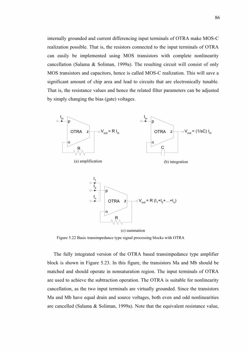
86
internally grounded and current differencing input terminals of OTRA make MOS-C
realization possible. That is, the resistors connected to the input terminals of OTRA
can easily be implemented using MOS transistors with complete nonlinearity
cancellation (Salama & Soliman, 1999a). The resulting circuit will consist of only
MOS transistors and capacitors, hence is called MOS-C realization. This will save a
significant amount of chip area and lead to circuits that are electronically tunable.
That is, the resistance values and hence the related filter parameters can be adjusted
by simply changing the bias (gate) voltages.
p
n
zOTRA
Iin
Vout = R Iin
R
(a) amplification
p
n
zOTRA
Iin
Vout = (1/sC) Iin
C
(b) integration
p
n
zOTRA
I1
Vout = R (I1+I2+…+In)
R
I2
In...
(c) summation
Figure 5.22 Basic transimpedance type signal processing blocks with OTRA
The fully integrated version of the OTRA based transimpedance type amplifier
block is shown in Figure 5.23. In this figure, the transistors Ma and Mb should be
matched and should operate in nonsaturation region. The input terminals of OTRA
are used to achieve the subtraction operation. The OTRA is suitable for nonlinearity
cancellation, as the two input terminals are virtually grounded. Since the transistors
Ma and Mb have equal drain and source voltages, both even and odd nonlinearities
are cancelled (Salama & Soliman, 1999a). Note that the equivalent resistance value,
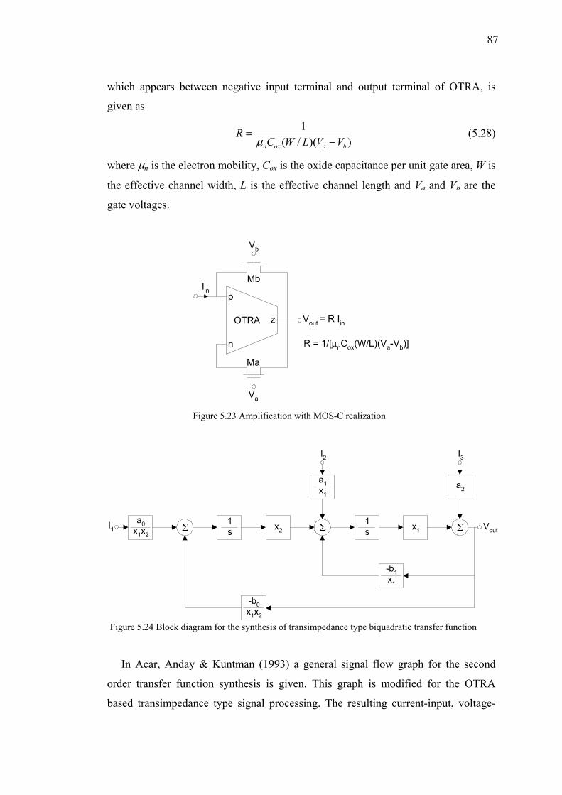
87
which appears between negative input terminal and output terminal of OTRA, is
given as
))(/(1
baoxn VVLWCR
−=µ
(5.28)
where µn is the electron mobility, Cox is the oxide capacitance per unit gate area, W is
the effective channel width, L is the effective channel length and Va and Vb are the
gate voltages.
p
n
zOTRA
Iin
Vout = R Iin
Vb
Mb
Va
Ma
R = 1/[µnCox(W/L)(Va-Vb)]
Figure 5.23 Amplification with MOS-C realization
a0x1x2
I1 Σ 1s x2 Σ 1
s x1 Σ Vout
-b1x1
-b0x1x2
a1x1
I2
a2
I3
Figure 5.24 Block diagram for the synthesis of transimpedance type biquadratic transfer function
In Acar, Anday & Kuntman (1993) a general signal flow graph for the second
order transfer function synthesis is given. This graph is modified for the OTRA
based transimpedance type signal processing. The resulting current-input, voltage-
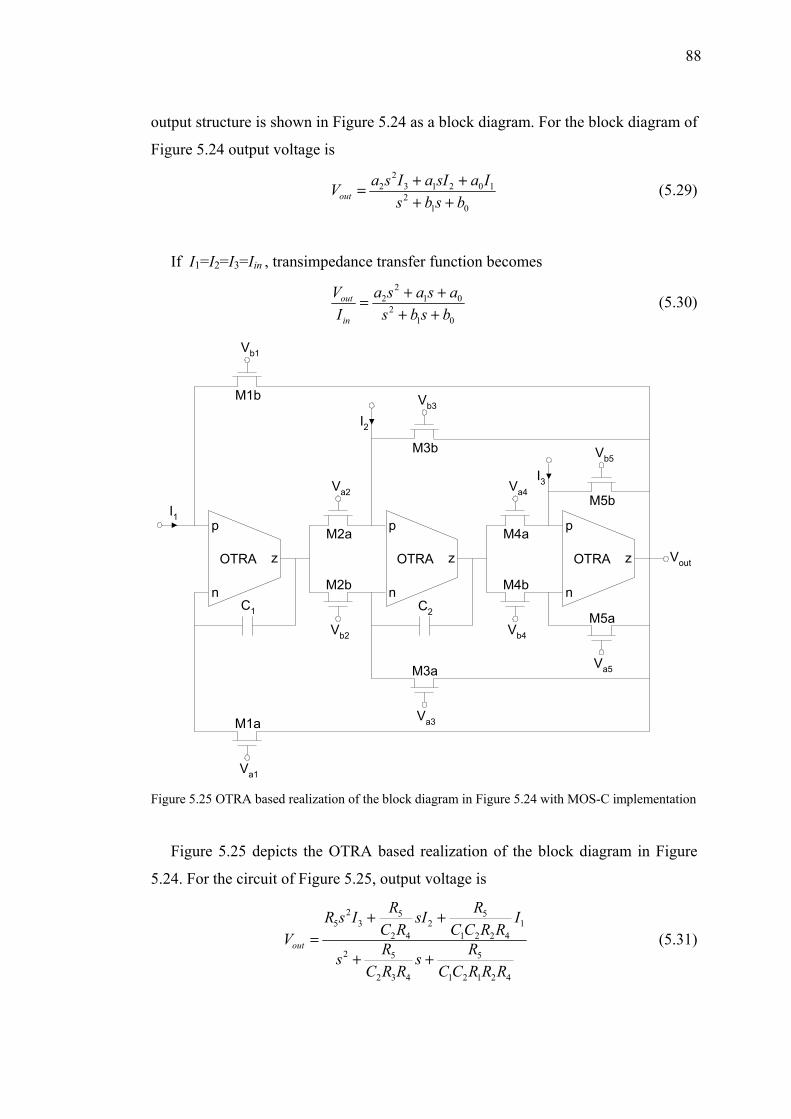
88
output structure is shown in Figure 5.24 as a block diagram. For the block diagram of
Figure 5.24 output voltage is
012
102132
2
bsbsIasIaIsaVout ++
++= (5.29)
If I1=I2=I3=Iin , transimpedance transfer function becomes
012
012
2
bsbsasasa
IV
in
out
++++= (5.30)
p
n
zOTRA Vout
Vb5
M5b
Va5
M5a
Va4
M4a
Vb4
M4b
p
n
zOTRA
C2
Va2
M2a
Vb2
M2b
p
n
zOTRA
I1
C1
Vb3
M3b
Va3
M3a
Vb1
M1b
Va1
M1a
I2
I3
Figure 5.25 OTRA based realization of the block diagram in Figure 5.24 with MOS-C implementation
Figure 5.25 depicts the OTRA based realization of the block diagram in Figure
5.24. For the circuit of Figure 5.25, output voltage is
42121
5
432
52
14221
52
42
53
25
RRRCCRs
RRCRs
IRRCC
RsIRC
RIsRVout
++
++= (5.31)
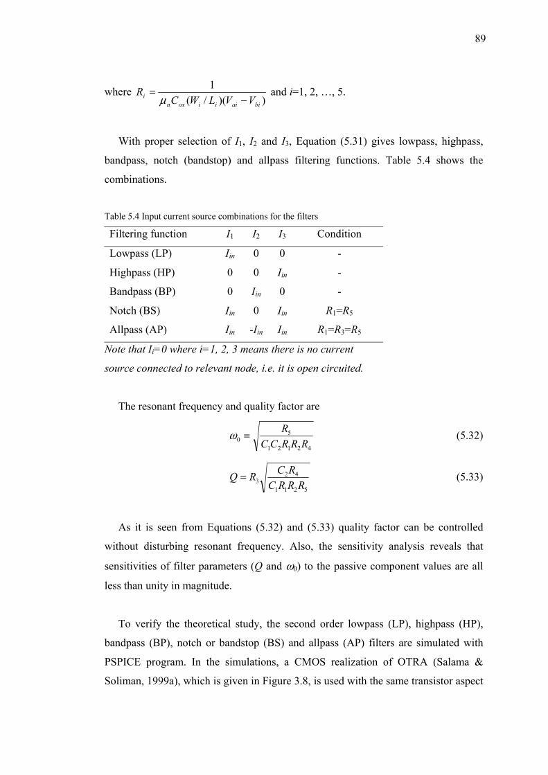
89
where ))(/(
1
biaiiioxni VVLWC
R−
=µ
and i=1, 2, …, 5.
With proper selection of I1, I2 and I3, Equation (5.31) gives lowpass, highpass,
bandpass, notch (bandstop) and allpass filtering functions. Table 5.4 shows the
combinations.
Table 5.4 Input current source combinations for the filters
Filtering function I1 I2 I3 Condition
Lowpass (LP) Iin 0 0 -
Highpass (HP) 0 0 Iin -
Bandpass (BP) 0 Iin 0 -
Notch (BS) Iin 0 Iin R1=R5
Allpass (AP) Iin -Iin Iin R1=R3=R5
Note that Ii=0 where i=1, 2, 3 means there is no current
source connected to relevant node, i.e. it is open circuited.
The resonant frequency and quality factor are
42121
50 RRRCC
R=ω (5.32)
5211
423 RRRC
RCRQ = (5.33)
As it is seen from Equations (5.32) and (5.33) quality factor can be controlled
without disturbing resonant frequency. Also, the sensitivity analysis reveals that
sensitivities of filter parameters (Q and ω0) to the passive component values are all
less than unity in magnitude.
To verify the theoretical study, the second order lowpass (LP), highpass (HP),
bandpass (BP), notch or bandstop (BS) and allpass (AP) filters are simulated with
PSPICE program. In the simulations, a CMOS realization of OTRA (Salama &
Soliman, 1999a), which is given in Figure 3.8, is used with the same transistor aspect
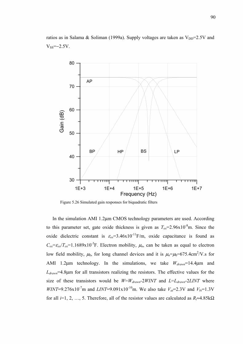
90
ratios as in Salama & Soliman (1999a). Supply voltages are taken as VDD=2.5V and
VSS=−2.5V.
1E+3 1E+4 1E+5 1E+6 1E+7Frequency (Hz)
30
40
50
60
70
80G
ain
(dB)
AP
BP HP LPBS
Figure 5.26 Simulated gain responses for biquadratic filters
In the simulation AMI 1.2µm CMOS technology parameters are used. According
to this parameter set, gate oxide thickness is given as Tox=2.96x10⁻⁸m. Since the
oxide dielectric constant is εox=3.46x10⁻¹¹F/m, oxide capacitance is found as
Cox=εox/Tox=1.1689x10-3F. Electron mobility, µn, can be taken as equal to electron
low field mobility, µ0, for long channel devices and it is µn=µ0=675.4cm2/V.s for
AMI 1.2µm technology. In the simulations, we take Wdrawn=14.4µm and
Ldrawn=4.8µm for all transistors realizing the resistors. The effective values for the
size of these transistors would be W=Wdrawn-2WINT and L=Ldrawn-2LINT where
WINT=9.276x10⁻⁷m and LINT=9.091x10⁻¹⁰m. We also take Vai=2.3V and Vbi=1.3V
for all i=1, 2, …, 5. Therefore, all of the resistor values are calculated as Ri≈4.85kΩ
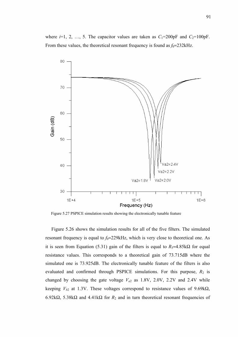
91
where i=1, 2, …, 5. The capacitor values are taken as C1=200pF and C2=100pF.
From these values, the theoretical resonant frequency is found as f0≈232kHz.
Figure 5.27 PSPICE simulation results showing the electronically tunable feature
Figure 5.26 shows the simulation results for all of the five filters. The simulated
resonant frequency is equal to f0≈229kHz, which is very close to theoretical one. As
it is seen from Equation (5.31) gain of the filters is equal to R5≈4.85kΩ for equal
resistance values. This corresponds to a theoretical gain of 73.715dB where the
simulated one is 73.925dB. The electronically tunable feature of the filters is also
evaluated and confirmed through PSPICE simulations. For this purpose, R2 is
changed by choosing the gate voltage Va2 as 1.8V, 2.0V, 2.2V and 2.4V while
keeping Vb2 at 1.3V. These voltages correspond to resistance values of 9.69kΩ,
6.92kΩ, 5.38kΩ and 4.41kΩ for R2 and in turn theoretical resonant frequencies of
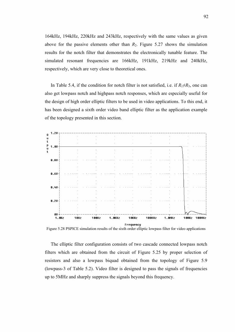
92
164kHz, 194kHz, 220kHz and 243kHz, respectively with the same values as given
above for the passive elements other than R2. Figure 5.27 shows the simulation
results for the notch filter that demonstrates the electronically tunable feature. The
simulated resonant frequencies are 166kHz, 191kHz, 219kHz and 240kHz,
respectively, which are very close to theoretical ones.
In Table 5.4, if the condition for notch filter is not satisfied, i.e. if R1≠R5, one can
also get lowpass notch and highpass notch responses, which are especially useful for
the design of high order elliptic filters to be used in video applications. To this end, it
has been designed a sixth order video band elliptic filter as the application example
of the topology presented in this section.
Figure 5.28 PSPICE simulation results of the sixth order elliptic lowpass filter for video applications
The elliptic filter configuration consists of two cascade connected lowpass notch
filters which are obtained from the circuit of Figure 5.25 by proper selection of
resistors and also a lowpass biquad obtained from the topology of Figure 5.9
(lowpass-3 of Table 5.2). Video filter is designed to pass the signals of frequencies
up to 5MHz and sharply suppress the signals beyond this frequency.
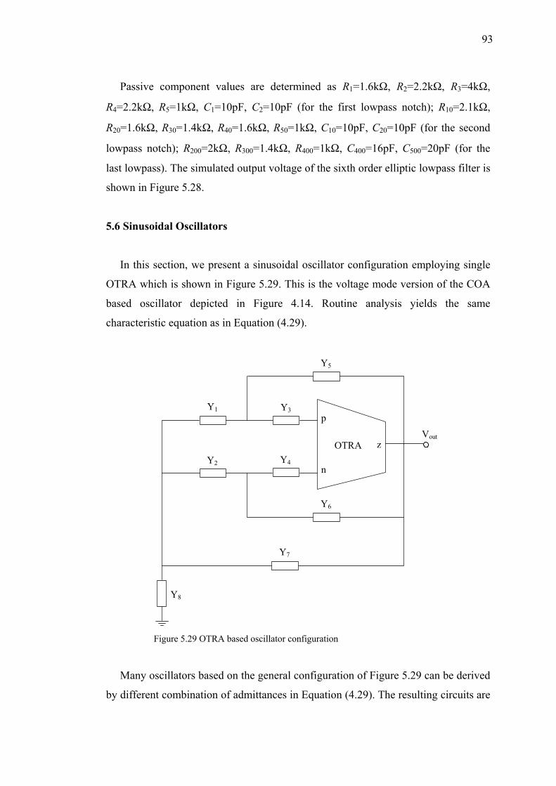
93
Passive component values are determined as R1=1.6kΩ, R2=2.2kΩ, R3=4kΩ,
R4=2.2kΩ, R5=1kΩ, C1=10pF, C2=10pF (for the first lowpass notch); R10=2.1kΩ,
R20=1.6kΩ, R30=1.4kΩ, R40=1.6kΩ, R50=1kΩ, C10=10pF, C20=10pF (for the second
lowpass notch); R200=2kΩ, R300=1.4kΩ, R400=1kΩ, C400=16pF, C500=20pF (for the
last lowpass). The simulated output voltage of the sixth order elliptic lowpass filter is
shown in Figure 5.28.
5.6 Sinusoidal Oscillators
In this section, we present a sinusoidal oscillator configuration employing single
OTRA which is shown in Figure 5.29. This is the voltage mode version of the COA
based oscillator depicted in Figure 4.14. Routine analysis yields the same
characteristic equation as in Equation (4.29).
p
n
zOTRAVout
Y1
Y2 Y4
Y5
Y3
Y8
Y6
Y7
Figure 5.29 OTRA based oscillator configuration
Many oscillators based on the general configuration of Figure 5.29 can be derived
by different combination of admittances in Equation (4.29). The resulting circuits are
94
given in Table 4.1. The oscillation conditions and the oscillation frequencies of these
circuits are tabulated in Table 4.2. As it can be seen from Tables 4.1 and 4.2, the first
four circuits are single frequency oscillators containing only two capacitors and two
resistors. Indeed, oscillator-1 corresponds to the OTRA based circuit proposed by
Salama & Soliman (2000). The oscillation frequency of the fifth circuit can
independently be adjusted by a grounded resistor without affecting the oscillation
condition. The OTRA based version of this single resistance controlled oscillator was
given in an early work (Çam, 2002). The remaining eight oscillators are new
realizations. If we interchange each capacitor with a resistor and each resistor with a
capacitor in oscillator-5, the resulting circuit is still a single resistance controlled
oscillator in the expense of using one more capacitor that violates the canonic
realization. With the last five circuits in Tables 4.1 and 4.2, it is possible to achieve
independent control on the oscillation condition without affecting the oscillation
frequency.
All of the tabulated circuits employ only two dynamical elements meaning that
the proposed oscillators are canonic. The single frequency oscillators utilize two
resistors. The remaining six circuits use three resistors for independent control of the
oscillation frequency or the oscillation condition. In this respect, they contain
minimum number of passive elements. It can easily be shown that all the passive
sensitivities of the oscillation frequencies are less than or equal to one half in
magnitude for all of the topologies.
To verify the theoretical study, the oscillator circuits have been simulated using
PSPICE program. As illustrating examples the simulation results of the OTRA based
single resistance controlled oscillator is given. For the circuit passive components are
chosen as R3=R8=1kΩ, R6=2kΩ, C2=C7=100pF, which result in 1.59MHz oscillation
frequency. The PSPICE simulations were performed using the CMOS realizations of
OTRA (Salama & Soliman, 1999a) given in Figure 3.8.
PSPICE simulations were performed on the basis of AMI 1.2µm MOS transistor
parameters. Supply voltages are taken as VDD=2.5V and VSS=−2.5V. According to
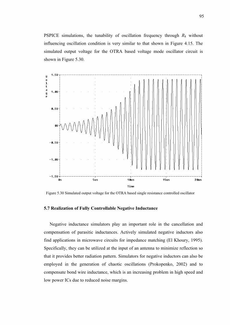
95
PSPICE simulations, the tunability of oscillation frequency through R8 without
influencing oscillation condition is very similar to that shown in Figure 4.15. The
simulated output voltage for the OTRA based voltage mode oscillator circuit is
shown in Figure 5.30.
Figure 5.30 Simulated output voltage for the OTRA based single resistance controlled oscillator
5.7 Realization of Fully Controllable Negative Inductance
Negative inductance simulators play an important role in the cancellation and
compensation of parasitic inductances. Actively simulated negative inductors also
find applications in microwave circuits for impedance matching (El Khoury, 1995).
Specifically, they can be utilized at the input of an antenna to minimize reflection so
that it provides better radiation pattern. Simulators for negative inductors can also be
employed in the generation of chaotic oscillations (Prokopenko, 2002) and to
compensate bond wire inductance, which is an increasing problem in high speed and
low power ICs due to reduced noise margins.
96
To help the understanding of a negative inductance, the difference between a
positive inductance, negative inductance and a capacitance is summarized in Table
5.5. Unlike capacitors, the magnitude of the negative inductance increases with
frequency the same way as positive inductances. On the other hand, it provides a
negative 90o phase the same way as capacitors.
Table 5.5 Comparison between inductance and capacitance
Positive inductance Negative inductance Positive capacitance
Impedance jωL -jωL -j/ωC
Magnitude ωL ωL 1/ωC
Phase 90o -90o -90o
Grounded inductor simulation using active elements such as op-amp, current
conveyor, current feedback op-amp and four terminal floating nullor has been
studied so far. A number of simulated grounded inductors are available in the
literature (Bruton, 1980; Çam, Çiçekoğlu & Kuntman, 2000; Çam et al., 2003;
Çiçekoğlu, 1998; Salama & Soliman, 2000; Senani, 1995; Senani, 1998). Universal
series and parallel immittance simulator topologies employing two four terminal
floating nullors are presented by Çam, Çiçekoğlu & Kuntman (2000), which simulate
negative inductance by choosing appropriate passive elements. General immittance
simulator circuits that enable simulation of all possible forms of inductors including
purely negative ones are proposed by Çiçekoğlu (1998). However, they use multiple
current conveyors. Recently, a positive inductor simulation using two OTRAs was
presented (Salama & Soliman, 1999a).
In this section, we present a realization of grounded negative inductance
employing single OTRA (Kılınç, Salama & Çam, 2006). Simulated negative inductor
provides full independent control on both the inductance value and the condition
with a capacitor and five resistors.
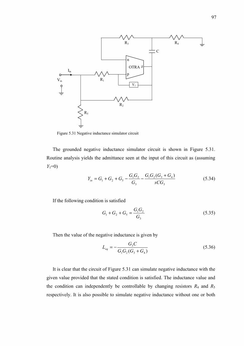
97
Y1
p
zn
OTRA
R1
Iin
Vin
R2
R3 R4
R5
C
Figure 5.31 Negative inductance simulator circuit
The grounded negative inductance simulator circuit is shown in Figure 5.31.
Routine analysis yields the admittance seen at the input of this circuit as (assuming
Y1=0)
3
4321
3
21521
)(sCG
GGGGGGGGGGYin
+−−++= (5.34)
If the following condition is satisfied
3
21521 G
GGGGG =++ (5.35)
Then the value of the negative inductance is given by
)( 4321
3
GGGGCG
Leq +−= (5.36)
It is clear that the circuit of Figure 5.31 can simulate negative inductance with the
given value provided that the stated condition is satisfied. The inductance value and
the condition can independently be controllable by changing resistors R4 and R5
respectively. It is also possible to simulate negative inductance without one or both
98
of these resistors. All possible cases with their corresponding conditions and
inductance values are listed in Table 5.6.
Table 5.6 All forms of fully controllable negative inductance realizations
Element choice Condition Leq Full control
G4=0, G5=0 3
2121 G
GGGG =+ 21GG
C− on condition
G4≠0, G5=0 3
2121 G
GGGG =+ )( 4321
3
GGGGCG+
− on Leq
G4=0, G5≠0 3
21521 G
GGGGG =++ 21GG
C− on condition
G4≠0, G5≠0 3
21521 G
GGGGG =++ )( 4321
3
GGGGCG+
− on both
The frequency response and Leq range of the presented circuit depend on the
realization of OTRA, the limitations on the values of passive elements and
technology used for manufacture. For the two current feedback op-amp (AD844’s of
Analog Devices) based implementation of OTRA (Çam et al., 2004) the circuit can
perform its function up to a few tens of megahertz whereas for some new CMOS
realizations of OTRA it can be beyond this. However, in the following, we introduce
a simple compensation method for high frequency applications.
As mentioned before, practically the transresistance gain is finite and its effect
should be considered. Also the frequency limitations associated with the OTRA
should be considered. Considering a single pole model and for high frequency
applications, the transresistance gain, Rm, can be expressed as in Equation (5.10).
For high frequency applications, compensation methods must be employed in
order to account for the error introduced in Equation (5.34). Considering the circuit
shown in Figure 5.31,
)()(
3
4321
3
21521 s
sCGGGGG
GGG
GGGYin ε
++−++= (5.37)
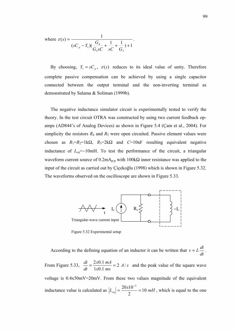
99
where 1)11)((
1)(
33
41 +++−
=
GsCsCGGYsC
sp
ε .
By choosing, , psCY =1 )(sε reduces to its ideal value of unity. Therefore
complete passive compensation can be achieved by using a single capacitor
connected between the output terminal and the non-inverting terminal as
demonstrated by Salama & Soliman (1999b).
The negative inductance simulator circuit is experimentally tested to verify the
theory. In the test circuit OTRA was constructed by using two current feedback op-
amps (AD844’s of Analog Devices) as shown in Figure 5.4 (Çam et al., 2004). For
simplicity the resistors R4 and R5 were open circuited. Passive element values were
chosen as R1=R2=1kΩ, R3=2kΩ and C=10nF resulting equivalent negative
inductance of Leq=−10mH. To test the performance of the circuit, a triangular
waveform current source of 0.2mAp-p with 100kΩ inner resistance was applied to the
input of the circuit as carried out by Çiçekoğlu (1998) which is shown in Figure 5.32.
The waveforms observed on the oscilloscope are shown in Figure 5.33.
Is Rst
−L
Triangular-wave current input
Figure 5.32 Experimental setup
According to the defining equation of an inductor it can be written that dtdiL=v .
From Figure 5.33, sAmsxmAx
dtdi /2
1.011.02 == and the peak value of the square wave
voltage is 0.4x50mV=20mV. From these two values magnitude of the equivalent
inductance value is calculated as mHxLeq 1021020 3
==−
, which is equal to the one
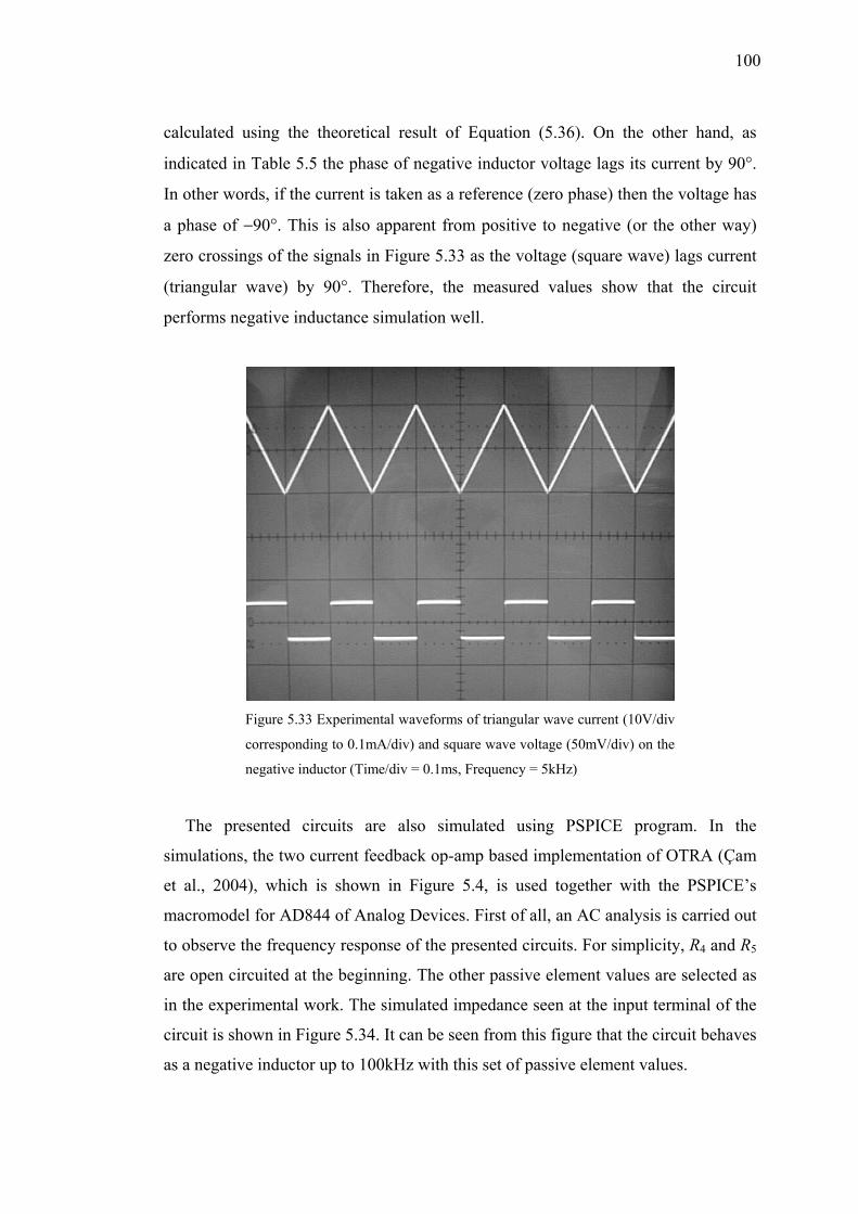
100
calculated using the theoretical result of Equation (5.36). On the other hand, as
indicated in Table 5.5 the phase of negative inductor voltage lags its current by 90°.
In other words, if the current is taken as a reference (zero phase) then the voltage has
a phase of −90°. This is also apparent from positive to negative (or the other way)
zero crossings of the signals in Figure 5.33 as the voltage (square wave) lags current
(triangular wave) by 90°. Therefore, the measured values show that the circuit
performs negative inductance simulation well.
Figure 5.33 Experimental waveforms of triangular wave current (10V/div
corresponding to 0.1mA/div) and square wave voltage (50mV/div) on the
negative inductor (Time/div = 0.1ms, Frequency = 5kHz)
The presented circuits are also simulated using PSPICE program. In the
simulations, the two current feedback op-amp based implementation of OTRA (Çam
et al., 2004), which is shown in Figure 5.4, is used together with the PSPICE’s
macromodel for AD844 of Analog Devices. First of all, an AC analysis is carried out
to observe the frequency response of the presented circuits. For simplicity, R4 and R5
are open circuited at the beginning. The other passive element values are selected as
in the experimental work. The simulated impedance seen at the input terminal of the
circuit is shown in Figure 5.34. It can be seen from this figure that the circuit behaves
as a negative inductor up to 100kHz with this set of passive element values.
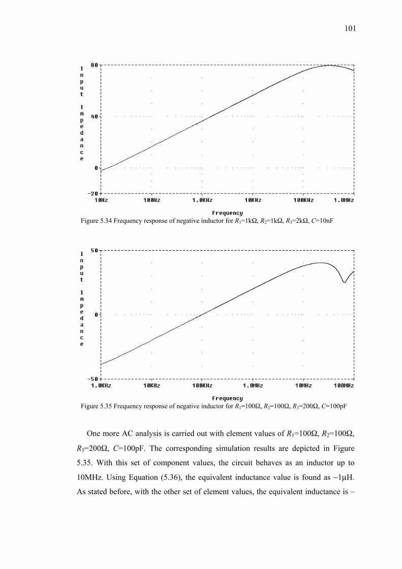
101
Figure 5.34 Frequency response of negative inductor for R1=1kΩ, R2=1kΩ, R3=2kΩ, C=10nF
Figure 5.35 Frequency response of negative inductor for R1=100Ω, R2=100Ω, R3=200Ω, C=100pF
One more AC analysis is carried out with element values of R1=100Ω, R2=100Ω,
R3=200Ω, C=100pF. The corresponding simulation results are depicted in Figure
5.35. With this set of component values, the circuit behaves as an inductor up to
10MHz. Using Equation (5.36), the equivalent inductance value is found as −1µH.
As stated before, with the other set of element values, the equivalent inductance is –
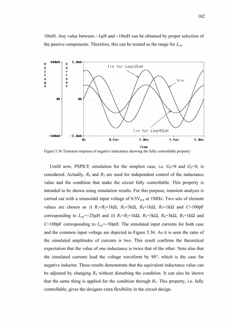
102
10mH. Any value between −1µH and −10mH can be obtained by proper selection of
the passive components. Therefore, this can be treated as the range for Leq.
Figure 5.36 Transient response of negative inductance showing the fully controllable property
Untill now, PSPICE simulation for the simplest case, i.e. G4=0 and G5=0, is
considered. Actually, R4 and R5 are used for independent control of the inductance
value and the condition that make the circuit fully controllable. This property is
intended to be shown using simulation results. For this purpose, transient analysis is
carried out with a sinusoidal input voltage of 0.5Vp-p at 1MHz. Two sets of element
values are chosen as i) R1=R2=1kΩ, R3=3kΩ, R4=1kΩ, R5=1kΩ and C=100pF
corresponding to Leq=−25µH and ii) R1=R2=1kΩ, R3=3kΩ, R4=3kΩ, R5=1kΩ and
C=100pF corresponding to Leq=−50µH. The simulated input currents for both case
and the common input voltage are depicted in Figure 5.36. As it is seen the ratio of
the simulated amplitudes of currents is two. This result confirms the theoretical
expectation that the value of one inductance is twice that of the other. Note also that
the simulated currents lead the voltage waveform by 90°, which is the case for
negative inductor. These results demonstrate that the equivalent inductance value can
be adjusted by changing R4 without disturbing the condition. It can also be shown
that the same thing is applied for the condition through R5. This property, i.e. fully
controllable, gives the designer extra flexibility in the circuit design.

103
Vin
Iin R=1kΩ L=1µH
Leq=-1µH
Figure 5.37 Circuit for the application of inductance cancellation
As stated earlier, one of the applications of negative inductor is to cancel the
unwanted inductance. To justify this application, the circuit of Figure 5.37 is
constructed and simulated using PSPICE. This circuit contains a resistor of 1kΩ in
series with a positive inductor of 1µH. The effect of the inductor is tried to cancel by
connecting a series negative inductor with the same inductance value in magnitude.
In this configuration, the presented negative inductor simulator is used with
R1=100Ω, R2=100Ω, R3=200Ω, C=100pF corresponding to Leq=−1µH. First of all,
the circuit in Figure 5.37 is simulated without the resistor and positive inductor, i.e.
R=0 and L=0. The simulation result for this case is shown in Figure 5.38 in which the
current leads voltage by 90° since the only remaining element is the negative
inductor. The theoretical peak value for the current in Figure 5.38 is calculated as
mAL
VI peakin
peakin 4010)102(
25.066
,, ≈
⋅⋅=
⋅= −πω
, which is very close to simulated one.
When we connect the resistor and the positive inductor, the simulation gives the
waveforms in Figure 5.39. In this figure, current and voltage are in phase since the
effect of inductor is cancelled by the negative inductor simulator making the circuit
purely resistive. One more transient simulation for Figure 5.37 is carried out by
applying a sinusoidal input voltage of 1Vp-p at 1MHz. The simulation results for this
case are shown in Figure 5.40 in which there is no distortion in the waveforms.
Therefore, we can say that the presented circuit works properly up to at least 1Vp-p.
This value can be much higher for other choice of element values.
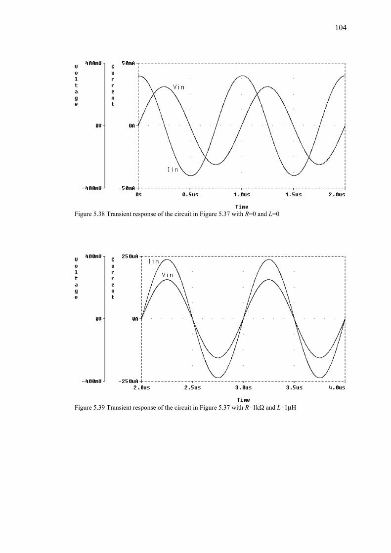
104
Figure 5.38 Transient response of the circuit in Figure 5.37 with R=0 and L=0
Figure 5.39 Transient response of the circuit in Figure 5.37 with R=1kΩ and L=1µH
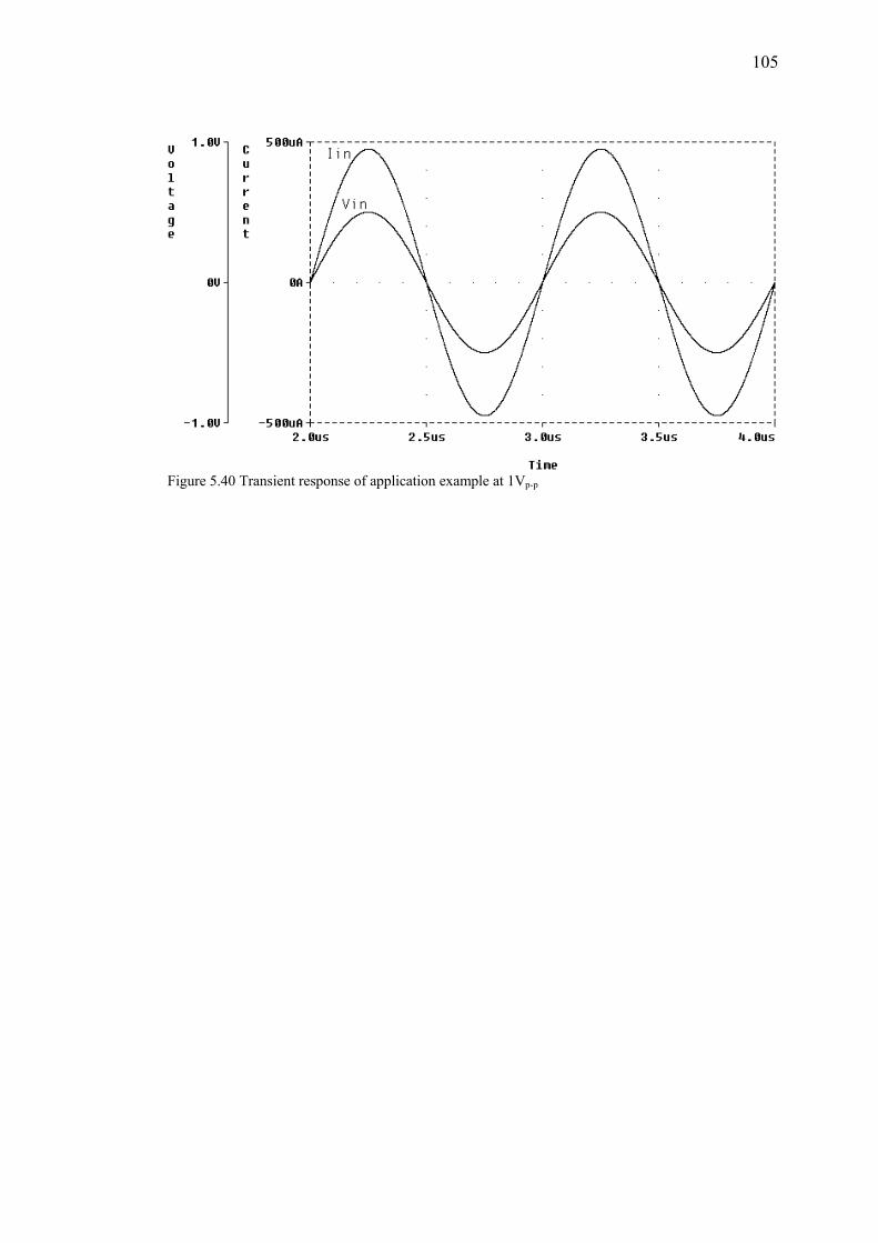
105
Figure 5.40 Transient response of application example at 1Vp-p
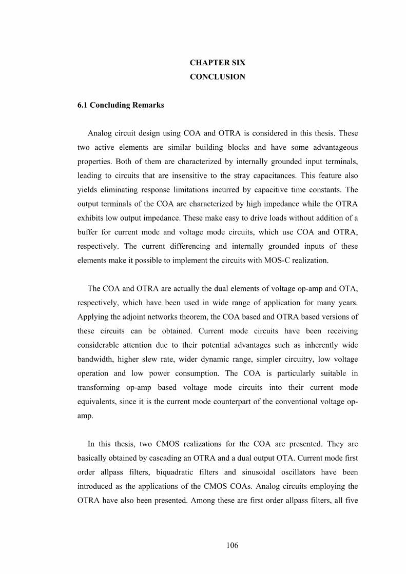
CHAPTER SIX
CONCLUSION
6.1 Concluding Remarks
Analog circuit design using COA and OTRA is considered in this thesis. These
two active elements are similar building blocks and have some advantageous
properties. Both of them are characterized by internally grounded input terminals,
leading to circuits that are insensitive to the stray capacitances. This feature also
yields eliminating response limitations incurred by capacitive time constants. The
output terminals of the COA are characterized by high impedance while the OTRA
exhibits low output impedance. These make easy to drive loads without addition of a
buffer for current mode and voltage mode circuits, which use COA and OTRA,
respectively. The current differencing and internally grounded inputs of these
elements make it possible to implement the circuits with MOS-C realization.
The COA and OTRA are actually the dual elements of voltage op-amp and OTA,
respectively, which have been used in wide range of application for many years.
Applying the adjoint networks theorem, the COA based and OTRA based versions of
these circuits can be obtained. Current mode circuits have been receiving
considerable attention due to their potential advantages such as inherently wide
bandwidth, higher slew rate, wider dynamic range, simpler circuitry, low voltage
operation and low power consumption. The COA is particularly suitable in
transforming op-amp based voltage mode circuits into their current mode
equivalents, since it is the current mode counterpart of the conventional voltage op-
amp.
In this thesis, two CMOS realizations for the COA are presented. They are
basically obtained by cascading an OTRA and a dual output OTA. Current mode first
order allpass filters, biquadratic filters and sinusoidal oscillators have been
introduced as the applications of the CMOS COAs. Analog circuits employing the
OTRA have also been presented. Among these are first order allpass filters, all five
106
107
different forms of second order filters, multifunction biquads, transimpedance type
biquadratic filters and sinusoidal oscillators. OTRA based circuits for the realization
of nth order voltage transfer function and fully controllable negative inductance are
also included. The workability of the presented circuits has been verified by PSPICE
simulation results. First order allpass filter and negative inductance simulator circuits
are also tested experimentally. The presented circuits constitute alternative
candidates to the existing topologies and provide further possibilities to the designers
in the realization of analog circuits.
6.2 Future Work
In this thesis, the emphasis is on the design of various analog circuits, such as
filters and oscillators, that use COA or OTRA. On the other hand, only two CMOS
realization examples for COA are presented. However, some attempts can be done to
improve the performance of these realizations and to introduce other CMOS COAs
and OTRAs for increasing the number of possible topologies. Also, bipolar and
BiCMOS implementations of these elements are open for investigation. Although
many new COA and OTRA based analog signal processing applications have been
presented in this thesis, the analog design of neural networks, fuzzy controllers and
nonlinear circuits are not considered. Furthermore, the COA and OTRA can also be
used in chaotic signal generator instead of op-amp and OTA, which is a very
important building block for chaotic communication networks.
108
REFERENCES
Aaserud, O., & Nielsen, I. R. (1995). Trends in current analog design – A panel
debate. Analog Integrated Circuits and Signal Processing, 7, 5-9.
Abou-Allam, E., & El-Masry, E. I. (1997). A 200 MHz steered current operational
amplifier in 1.2µ CMOS technology. IEEE Journal of Solid-State Circuits, 32,
245-249.
Abuelma’atti, M. T. (2000a). Universal current-mode filter using single four-terminal
floating nullor. Microelectronics Journal, 31, 123-127.
Abuelma’atti, M. T. (2000b). New sinusoidal oscillators with fully uncoupled control
of oscillation frequency and condition using three CCII+s. Analog Integrated
Circuits and Signal Processing, 24, 253-261.
Abuelma’atti, M. T., & Al-Zaher, H. A. (1999). Current-mode sinusoidal oscillator
using single FTFN. IEEE Transactions on Circuits and Systems-II, 46, 69-74.
Acar, C., Anday, F., & Kuntman, H. (1993). On the realization of OTA-C filters.
International Journal of Circuit Theory and Applications, 21, 331-341.
Acar, C., & Özoğuz, S. (1999). A new versatile building block: Current-differencing
buffered amplifier suitable for analog signal processing filter. Microelectronics
Journal, 30, 157-160.
Allen, P. E., & Holberg, D. R. (1987). CMOS analog circuit design. New York: Holt,
Rinehart and Winston Inc.
Allen, P. E., & Terry, M. B. (1980). The use of current amplifiers for high
performance voltage applications. IEEE Journal of Solid-State Circuits, SC-15
(2), 155-162.
109
Anday, F. (1977a). Realization of nth-order transfer functions using current
differencing amplifiers. International Journal of Electronics, 42 (6), 613-616.
Anday, F. (1977b). Active realization of nth-order lowpass transfer functions. IEEE
Transactions on Circuits and Systems, CAS-24 (12), 745-746.
Anday, F. (1982). Realization of Norton amplifier nth-order switched-capacitor
networks. International Journal of Electronics, 53 (3), 289-292.
Arbel, A. F., & Goldminz, L. (1992). Output stage for current-mode feedback
amplifiers, theory and applications. Analog Integrated Circuits and Signal
Processing, 2, 243-255.
Awad, I. A., & Soliman, A. M. (2000). Current operational amplifiers (COA):
CMOS realization and active compensation. Analog Integrated Circuits and
Signal Processing, 24, 141-152.
Bordewijk, L. J. (1956). Inter-reciprocity applied to electrical networks. Applied
Scientific Research, B-6, 1-74.
Brodie, J. H. (1978). Realization of nth order transfer functions using current
differencing amplifiers. International Journal of Electronics, 44 (6), 663-665.
Bruton, L. T. (1980). RC active circuits: Theory and design. USA: Prentice Hall.
Brunn, E. (1991). A differential-input differential output current-mode operational
amplifier. International Journal of Electronics, 7, 1048-1056.
Bruun, E. (1994). A high-speed CMOS current op-amp for very low supply voltage
operation. IEEE International Symposium on Circuits and Systems, 5, 509-512.

110
Budak, A. (1974). Passive and active network analysis and synthesis. Boston:
Houghton Mifflin.
Carlin, H. J. (1964). Singular network elements. IEEE Transactions on Circuit
Theory, CT-11, 67-72.
Celma, S., Martinez, P. A., & Carlosena, A. (1992). Minimal realization for single
resistance controlled sinusoidal oscillator using single CCII. Electronics Letters,
28, 443-444.
Chang, C. M. (1991a). Current-mode allpass/notch and bandpass filter using single
CCII. Electronics Letters, 27 (20), 1812-1813.
Chang, C. M. (1991b). Universal active current filters using single second-generation
current conveyor. Electronics Letters, 27 (18), 1614-1617.
Chang, C. M., & Lee, M. S. (1994). Universal voltage-mode filter with three inputs
and one output using three current conveyors and one voltage follower.
Electronics Letters, 30 (25), 2112-2113.
Chang, C. M., & Tu, S. H. (1999). Universal voltage-mode filter with four inputs and
one output using two CCII+s. International Journal of Electronics, 86 (3), 305-
309.
Chen, J. J., Tsao, H. W., & Chen, C. C. (1992). Operational transresistance amplifier
using CMOS technology. Electronics Letters, 28, 2087-2088.
Chen, J. J., Tsao, H. W., Liu, S. I., & Chiu, W. (1995). Parasitic capacitance
insensitive current-mode filters using operational transresistance amplifier. IEE
Proceedings Part G – Circuits, Devices and Systems, 142, 186-192.
111
Cheng, K. H., & Wang, H. C. (1998). Design and analysis of low-voltage current
mode operational amplifier with differential-input and differential-output.
International Journal of Electronics, 85 (4), 443-453.
Comer, D. J., & McDermid, J. E. (1968). Inductorless bandpass characteristics using
all-pass networks. IEEE Transactions on Circuit Theory, CT-15, 501-503.
Comer, D. T., Comer, D. J., & Gonzalez, J. R. (1997). A high-frequency integrable
bandpass filter configuration. IEEE Transactions on Circuits and Systems-II, 44
(10), 856-861.
Çam, U. (2002). A novel single-resistance-controlled sinusoidal oscillator employing
single operational transresistance amplifier. Analog Integrated Circuits and Signal
Processing, 32, 183-186.
Çam, U., Çakır, C., & Çiçekoğlu O. (2004). Novel transimpedance type first-order
all-pass filter using single OTRA. AEÜ International Journal of Electronics and
Communications, 58, 296-298.
Çam, U., Çiçekoğlu, O., Gülsoy, M., & Kuntman, H. (2000). New voltage and
current mode first-order all-pass filters using single FTFN. Frequenz, 7 (8), 177-
179.
Çam, U., Çiçekoğlu, O., & Kuntman, H. (2000). Universal series and parallel
immittance simulators using four terminal floating nullors. Analog Integrated
Circuits and Signal Processing, 25, 59-66.
Çam, U., Kaçar, F., Çiçekoğlu, O., Kuntman, H., & Kuntman, A. (2003). Novel
grounded parallel immittance simulator topologies employing single OTRA. AEÜ
International Journal of Electronics and Communications, 57 (4), 287-290.
112
Çam, U., Kaçar, F., Çiçekoğlu, O., Kuntman, H., & Kuntman, A. (2004). Novel two
OTRA-based grounded immittance simulator topologies. Analog Integrated
Circuits and Signal Processing, 39, 169-175.
Çam, U., Kuntman, H., & Acar, C. (1998). On the realization of OTA-C oscillators.
International Journal of Electronics, 85, 313-326.
Çam, U., Toker, A., Çiçekoğlu, O., & Kuntman, H. (2000). Current-mode high
output impedance sinusoidal oscillator configuration employing single FTFN.
Analog Integrated Circuits and Signal Processing, 24, 231-238.
Çiçekoğlu, O. (1998). Active simulation of grounded inductors with CCII+s and
grounded passive elements. International Journal of Electronics, 85, 455-462.
Çiçekoğlu, O., Kuntman, H., & Berk, S. (1999). Single CCII+ based all-pass filters.
International Journal of Electronics, 86 (8), 947-955.
Director, S. W., & Rohrer, R. A. (1969). The generalised adjoint network and
network sensitivities. IEEE Transactions on Circuit Theory, CT-16, 318-323.
El Khoury, S. (1995). The design of active floating positive and negative inductors in
MMIC technology. IEEE Microwave and Guided Wave Letters, 5, 321-323.
Elwan, H. O., & Soliman, A. M. (1996). CMOS differential current conveyors and
applications for analog VLSI. Analog Integrated Circuits and Signal Processing,
11, 35-45.
Elwan, H. O., Soliman, A. M., & Ismail, M. (2001). A CMOS Norton amplifier-
based digitally controlled VGA for low-power wireless applications. IEEE
Transactions on Circuits and Systems-II, 48, 245-254.
113
Fabre, A. (1995a). Guest editorial. Analog Integrated Circuits and Signal
Processing, 7, 71-73.
Fabre, A. (1995b). Third-generation current conveyor: a new helpful active element.
Electronics Letters, 31, 338-339.
Haritantis, I. (1985). General method for designing RC harmonic oscillators.
International Journal of Electronics, 58, 295-305.
Higashimura, M. (1991). Current-mode allpass filter using FTFN with grounded
capacitor. Electronics Letters, 27, 1182-1183.
Higashimura, M. (1993). Current-mode lowpass, bandpass and highpass filter using
an FTFN. Microelectronics Journal, 24, 659-662.
Higashimura, M., & Fukiu, Y. (1988). Realisation of all-pass and notch filters a
single current conveyor. International Journal of Electronics, 65, 823-828.
Horng, J. W., Lay, J. R., Chang, C. W., & Lee, M. H. (1997). High input impedance
voltage-mode multifunction filters using plus-type CCIIs. Electronics Letters, 33,
472-473.
Kauert, R., Budde, W., & Kalz, A. (1995). A monolithic field segment photo sensor
system. IEEE Journal of Solid-State Circuits, 30, 807-811.
Kaulberg, T. (1993). A CMOS current-mode operational amplifier. IEEE Journal of
Solid-State Circuits, 28, 848-952.
Keskin, A. Ü., & Hancıoğlu, E. (2005). Current mode multifunction filter using two
CDBAs, AEÜ International Journal of Electronics and Communications, 59 (8),
495-498.
114
Kılınç, S., & Çam, U. (2003a). Yeni akım-modlu birinci derece tüm geçiren süzgeç
tasarımı. SİU’2003 11. Sinyal İşleme ve İletişim Uygulamaları Kurultayı, 219-
222.
Kılınç, S., & Çam, U. (2003b). Current operational amplifier based first-order allpass
filter. European Conference on Circuit Theory and Design, 2, 45-48.
Kılınç, S., & Çam, U. (2003c). Current-mode biquads using a single current
operational amplifier. TAINN’2003 Turkish Symposium on Artificial Intelligence
and Neural Networks, 290-292.
Kılınç, S., & Çam, U. (2003d). Akım modlu alçak ve yüksek geçiren süzgeçlerin
akım işlemsel kuvvetlendirici ile gerçeklenmesi. Elektrik, Elektronik ve Bilgisayar
Mühendisliği 10. Ulusal Kongresi, 314-317.
Kılınç, S., & Çam, U. (2003e). Akım işlemsel kuvvetlendirici kullanarak
ayarlanabilir frekanslı osilatör tasarımı. Elektrik, Elektronik ve Bilgisayar
Mühendisliği 10. Ulusal Kongresi, 318-321.
Kılınç, S., & Çam, U. (2003f). Current-mode oscillator configuration using single
current operational amplifier. ELECO’2003 International Conference on
Electrical and Electronics Engineering, 107-111.
Kılınç, S., & Çam, U. (2003g). İkinci derece alçak, yüksek ve bant geçiren
süzgeçlerin tek bir OTRA kullanarak gerçeklenmesi. SİU’2003 11. Sinyal İşleme
ve İletişim Uygulamaları Kurultayı, 215-218.
Kılınç, S., & Çam, U. (2003h). A new biquadratic filter configuration employing a
single operational transresistance amplifier. European Conference on Circuit
Theory and Design, 1, 275-278.
115
Kılınç, S., & Çam, U. (2004a). Current-mode first-order allpass filter employing
single current operational amplifier. Analog Integrated Circuits and Signal
Processing, 41, 47-53.
Kılınç, S., & Çam, U. (2004b). İşlemsel geçiş-direnç kuvvetlendirici (OTRA)
kullanılarak gerçeklenmiş tüm geçiren süzgeçler. SİU’2004 12. Sinyal İşleme ve
İletişim Uygulamaları Kurultayı, 133-136.
Kılınç, S., & Çam, U. (2004c). Operational transresistance amplifier based first-order
allpass filter with an application example. IEEE International Midwest
Symposium on Circuits and Systems, 1, 65-68.
Kılınç, S., & Çam, U. (2005a). Cascadable allpass and notch filters employing single
operational transresistance amplifier. Computers & Electrical Engineering, 31,
391-401.
Kılınç, S., & Çam, U. (2005b). İşlemsel geçiş-direnç kuvvetlendirici (OTRA)
kullanarak yüksek-dereceli gerilim transfer fonksiyonu gerçeklemesi. Elektrik,
Elektronik ve Bilgisayar Mühendisliği 11. Ulusal Kongresi, 1, 129-132.
Kılınç, S., & Çam, U. (2005c). Realization of nth-order voltage transfer function
using single operational transresistance amplifier. ETRI Journal, 27, 647-650.
Kılınç, S., & Çam, U. (2005d). Transimpedance type signal processing using
operational transresistance amplifier (OTRA). ELECO’2005 International
Conference on Electrical and Electronics Engineering, 14-18.
Kılınç, S., & Çam, U. (2006). Transimpedance type fully integrated biquadratic
filters using operational transresistance amplifiers. Analog Integrated Circuits and
Signal Processing, 47 (2), 193-198.
116
Kılınç, S., Salama, K. N., & Çam, U. (2006). Realization of fully controllable
negative inductance with single operational transresistance amplifier. Circuits,
Systems and Signal Processing, 25, 47-57.
Koli, K. (2000). CMOS current amplifiers: Speed versus nonlinearity. Espoo:
Helsinki University of Technology Electronic Circuit Design Laboratory.
Laker, K. R., & Sansen, W. M. C. (1994). Design of analog integrated circuits and
systems. Singapore: McGraw-Hill.
Laopoulos, T., Siskos, S., Bafleur, M., Givelin, P., & Tornier, E. (1995). Design and
applications of an easily integrable CMOS operational floating amplifier for the
meghertz range. Analog Integrated Circuits and Signal Processing, 7, 103-111.
Liu, S. I. (1995). Universal filter using two current-feedback amplifiers. Electronics
Letters, 31, 629-630.
Liu, S. I., Chen, J. J., Tsao, H. W., & Tsay, J. H. (1993). Design of biquad filters
with a single current follower. IEE Proceedings Part G – Circuits, Devices and
Systems, 140, 165-170.
Liu, S. I., & Hwang, C. S. (1997). Realisation of current-mode filters using single
FTFN. International Journal of Electronics, 82, 499-502.
Liu, S. I., & Lee, J. L. (1996). Insensitive current/voltage-mode filters using FTFNs.
Electronics Letters, 32, 1079-1080.
Liu, S. I., & Lee, J. L. (1997). Voltage-mode universal filters using two current
conveyors. International Journal of Electronics, 82, 145-149.
Liu, S. I., & Tsao, H. W. (1991). The single CCII biquads with high-input
impedance. IEEE Transactions on Circuits and Systems, 38, 456-461.
117
Liu, S. I., Tsao, H. W., & Wu, J. (1990). Cascadable current-mode single CCII
biquads. Electronics Letters, 26, 2005-2006.
Magram, L., & Arbel, A. (1994). Current-mode feedback amplifier employing a
transistorized feedback network. IEEE International Symposium on Circuits and
Systems, 5, 607-610.
Minaei, S., Çiçekoğlu, O., Kuntman, H., Dündar, G., & Cerid, O. (2003). New
realizations of current-mode and voltage-mode multifunction filters without
external passive elements. AEÜ International Journal of Electronics and
Communications, 57 (1), 63-69.
Moschytz, G. S. (1972). A high Q, insensitive active RC network, similar to the
Tarmy-Ghausi circuit but using single-ended operational amplifiers. Electronics
Letters, 8, 458-459.
Mucha, I. (1995). Current operational amplifiers: Basic architectures, properties,
exploitation and future. Analog Integrated Circuits and Signal Processing, 7, 243-
255.
Nagasaku, T., Hyogo, A., & Sekine, K. (1996). A synthesis of a novel current-mode
operational amplifier. Analog Integrated Circuits and Signal Processing, 11, 183-
185.
Palmisano, G., Palumbo, G., & Pennisi, S. (1999). CMOS current amplifiers. USA:
Kluwer Academic Publishers.
Palmisano, G., Palumbo, G., & Pennisi, S. (2000). Solutions for CMOS current
amplifiers with high-drive output stages. IEEE Transactions on Circuits and
Systems-II, 47 (10), 988-998.
118
Payne, A., & Toumazou, C. (1996). Analog amplifiers: classification and
generalization. IEEE Transactions on Circuits and Systems-I, 43, 43-50.
Penfield, P., Spence, R., & Duinker, S. (1970). Tellegen’s theorem and electrical
networks. Cambridge: MIT Press.
Prokopenko, V. G. (2002). Chaotic oscillator with negative inductance. Journal of
Communications Technology and Electronics, 47, 1131-1133.
Ravindran, A., Savla, A., Younus, I., & Ismail, M. (2002). A 0.8V CMOS filter
based on a novel low voltage operational transresistance amplifier. IEEE
International Midwest Symposium on Circuits and Systems, 3, 368-371.
Roberts, G. W., & Sedra, A. S. (1989). All current-mode frequency selective circuits.
Electronics Letters, 25 (12), 759-760.
Roberts, G. W., & Sedra, A. S. (1992). A general class of current amplifier-based
biquadratic filter circuits. IEEE Transactions on Circuits and Systems-I, 39, 257-
263.
Salama, K. N., & Soliman, A. M. (1999a). CMOS operational transresitance
amplifier for analog signal processing applications. Microelectronics Journal, 30,
235-245.
Salama, K. N., & Soliman, A. M. (1999b). Universal filters using operational
transresistance amplifiers. AEÜ International Journal of Electronics and
Communications, 53 (1), 49-52.
Salama, K. N., & Soliman, A. M. (2000). Novel oscillators using the operational
transresitance amplifier. Microelectronics Journal, 31, 39-47.
119
Schauman, R., & Van Valkenburg, M. E. (2001). Design of analog filters. New
York: Oxford University Press.
Sedra, A., & Smith, K. (1970). A second-generation current-conveyor and its
applications. IEEE Transactions on Circuit Theory, CT-17, 132-134.
Senani, R. (1994). On equivalent forms of single op-amp sinusoidal RC oscillators.
IEEE Transactions on Circuits and Systems-I, 41, 617-624.
Senani, R. (1995). Universal linear voltage-controlled impedance configuration. IEE
Proceedings Part G – Circuits, Devices and Systems, 142, 208.
Senani, R. (1998). Realisation of a class of analog signal processing/signal
generation circuits: Novel configurations using current feedback op-amps.
Frequenz, 52, 106-206.
Smith, K., & Sedra, A. (1968). The current-conveyor - a new circuit building block.
IEEE Proceedings, 56, 1368-69.
Soliman, A. M. (1998). Current-mode oscillator using single output current
conveyor. Microelectronics Journal, 29, 907-912.
Soliman, A. M. (2000). Current feedback operational amplifier based oscillators.
Analog Integrated Circuits and Signal Processing, 23, 45-55.
Takagi, S. (2001). Analog circuit designs in the last decade and their trends toward
21st century. IEICE Trans. Fundamentals, E84-A (1), 68-79.
Tangsritat, W., Surakampontorn, W., & Fujii, N. (2003). Realization of leapfrog
filters using current differential buffered amplifiers. IEICE Trans. Fundamentals,
E86-A, 318-326.
120
Tarmy, R., & Ghausi, M. S. (1970). Very high Q, insensitive active RC networks.
IEEE Transactions on Circuit Theory, CT-17, 358-366.
Tellegen, B. D. H. (1951). Theorie der electrishe netwerken. Noordhof, Groningen.
Tellegen, B. D. H. (1952). A general network theorem with applications. Philips
Res. Rep., 7, 259-269.
Tellegen, B. D. H. (1954). La recherche pour una serie complete d’elements de
circuit ideaux non-lineaires. Rendiconti-Seminario Matematico e Fisico di
Milano, 25, 134-144.
Toker, A., Kuntman, H., Çiçekoğlu, O., & Dişçigil, M. (2002). New oscillator
topologies using inverting second-generation current conveyors. Turkish Journal
of Electrical Engineering and Computer Sciences (ELEKTRİK), 10 (1), 119-129.
Toker, A., Özoğuz, S., Çiçekoğlu, O., & Acar, C. (2000). Current-mode all-pass
filters using current differencing buffered amplifier and new high-Q bandpass
filter configuration. IEEE Transactions on Circuits and Systems-II, 47, 949-954.
Toumazou, C., Lidjey, F. J., & Haigh, D. (1990). Analog IC design: The current-
mode approach. UK: Peter Peregrinus.
Van den Broeke, L., & Nieuwkerk, A. (1993). Wide-band integrated receiver with
improved dynamic range using a current switch at the input. IEEE Journal of
Solid-State Circuits, 28, 862-864.
Vanisri, T., & Toumazou, C. (1992). On the design of low-noise current-mode
optical preamplifiers. Analog Integrated Circuits and Signal Processing, 2, 179-
195.
121
Wang, Z. (1990). Wideband class AB (push-pull) current amplifier in CMOS
technology. Electronics Letters, 26 (8), 543-545.
Wilson, B. (1990). Recent developments in current conveyors and current-mode
circuits, IEE Proceedings Part G – Circuits, Devices and Systems, 137 (2), 63-77.
Yen, R. C., & Gray, P. R. (1982). A MOS switched-capacitor instrumentation
amplifier. IEEE Journal of Solid-State Circuits, 28, 1008-1013.
Youssef, M. A., & Soliman, A. M. (2005). A novel CMOS realization of the
differential input balanced output current operational amplifier and its
applications. Analog Integrated Circuits and Signal Processing, 44, 37-53.
Zele, R. H., Allstot, D. J., & Fiez, T. S. (1991). Fully-differential CMOS current-
mode circuits and applications. IEEE International Symposium on Circuits and
Systems, 3, 1817-1820.