Embed Size (px)
Citation preview
Analysis and Practical Relevance of CM/DM EMI
Noise Separator Characteristics
Sebastian Schroth1, Florian Krismer1, Johann W. Kolar1, Hans Ertl21Power Electronic Systems Laboratory, ETH-Zurich, Switzerland
2Vienna University of Technology, AustriaEmail: [email protected], [email protected],
[email protected], [email protected]: http://www.pes.ee.ethz.ch
Keywords
<<EMC/EMI>>, <<Noise>>.
Abstract
This Paper details two different contributions related to practical CM/DM EMI measurements.A first part investigates sources and implications of measurement errors that result for CM/DMseparators in a practical measurement environment with a particular focus on the recentlypresented input impedance criterion for CM/DM separators. Furthermore, the realization of anactive CM/DM separator, which features competitive separation capabilities (DMTR/CMRR >51 dB and CMTR/DMRR > 47 dB for frequencies up to 10MHz), is presented.
Introduction
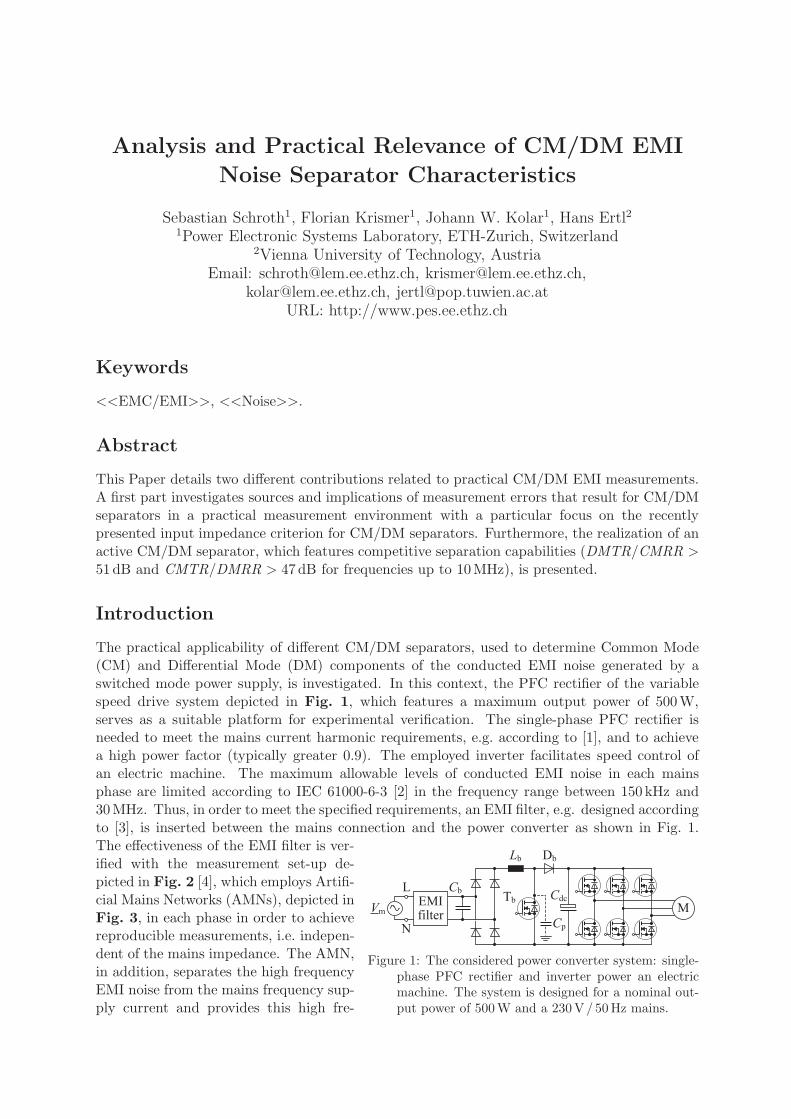
The practical applicability of different CM/DM separators, used to determine Common Mode(CM) and Differential Mode (DM) components of the conducted EMI noise generated by aswitched mode power supply, is investigated. In this context, the PFC rectifier of the variablespeed drive system depicted in Fig. 1, which features a maximum output power of 500W,serves as a suitable platform for experimental verification. The single-phase PFC rectifier isneeded to meet the mains current harmonic requirements, e.g. according to [1], and to achievea high power factor (typically greater 0.9). The employed inverter facilitates speed control ofan electric machine. The maximum allowable levels of conducted EMI noise in each mainsphase are limited according to IEC 61000-6-3 [2] in the frequency range between 150 kHz and30MHz. Thus, in order to meet the specified requirements, an EMI filter, e.g. designed accordingto [3], is inserted between the mains connection and the power converter as shown in Fig. 1.
Vm
Lb
Tb
CbL
N
Db
Cdc
M
Cp
Figure 1: The considered power converter system: single-phase PFC rectifier and inverter power an electricmachine. The system is designed for a nominal out-put power of 500W and a 230V/ 50Hz mains.
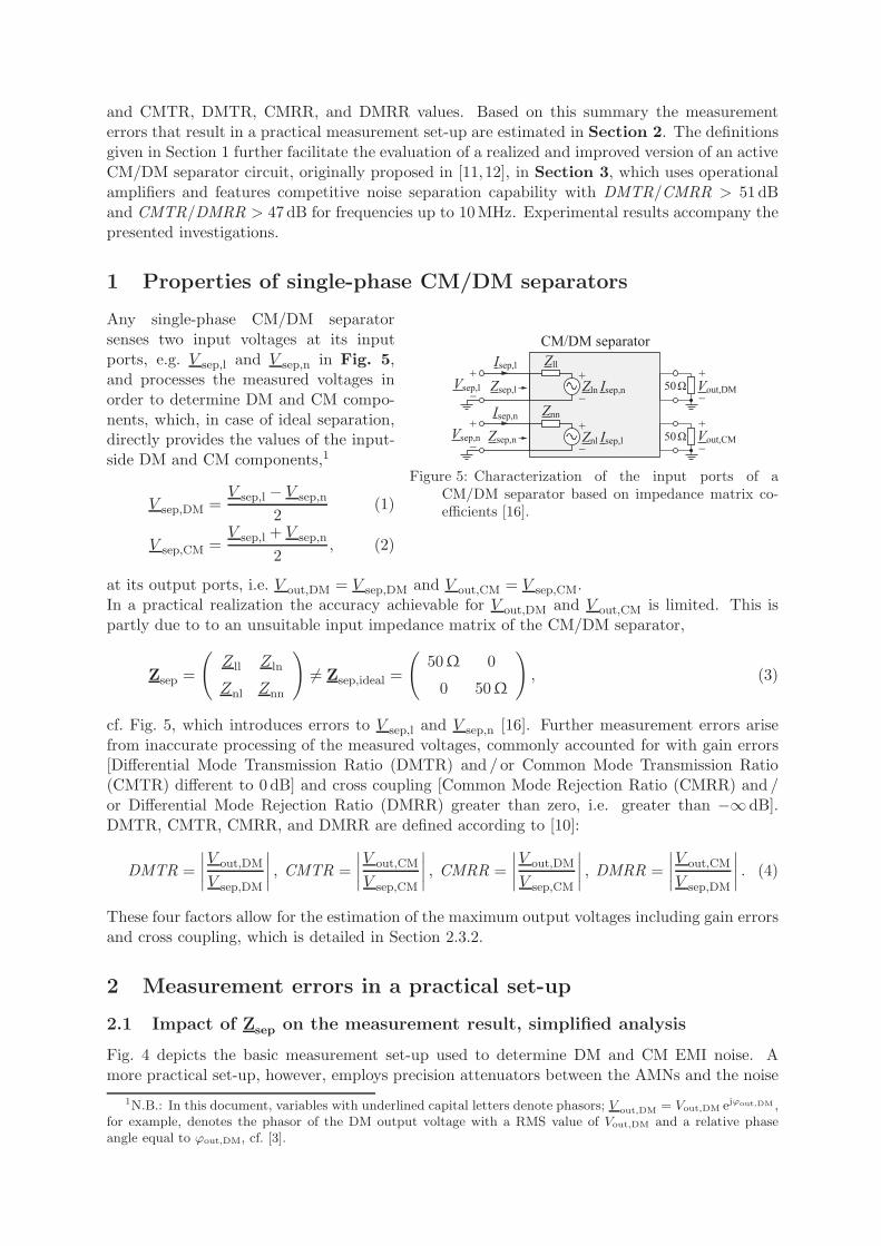
The effectiveness of the EMI filter is ver-ified with the measurement set-up de-picted in Fig. 2 [4], which employs Artifi-cial Mains Networks (AMNs), depicted inFig. 3, in each phase in order to achievereproducible measurements, i.e. indepen-dent of the mains impedance. The AMN,in addition, separates the high frequencyEMI noise from the mains frequency sup-ply current and provides this high fre-
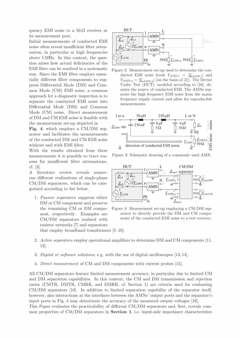
quency EMI noise to a 50Ω receiver atits measurement port.
Vs,CM
−
+2Vs,DM−
Zs,xZs,a
Zs,b
+
DUTl
n
PE
N
L
50 Ω 50 ΩVAMN,n VAMN,l
Vm
AMN
AMN
Figure 2: Measurement set-up used to determine the con-ducted EMI noise levels VAMN,l = |V AMN,l| andVAMN,n = |V AMN,n| (on the basis of [4]). The DeviceUnder Test (DUT), modeled according to [16], de-notes the source of conducted EMI. The AMNs sep-arate the high frequency EMI noise from the mainsfrequency supply current and allow for reproduciblemeasurements.
l or n 50 μH 250 μH
10 Ω250 nF
L or N
8 μF5 Ω
4 μFZAMN
Zm
ZAMN,0
50 ΩVAMN
direction of conducted EMI noise
EM
I m
eas.
mai
ns
PE
Figure 3: Schematic drawing of a commonly used AMN.
PE50 Ω
50 Ω
VAMN,n
VAMN,l
CM/DM
separator
Vs,CM
−
+2Vs,DM−
Zs,xZs,a
Zs,b
+
DUTl
nAMN
AMN
Zsep,n
L
N
Zsep,l
Vout,DM
Vout,CM
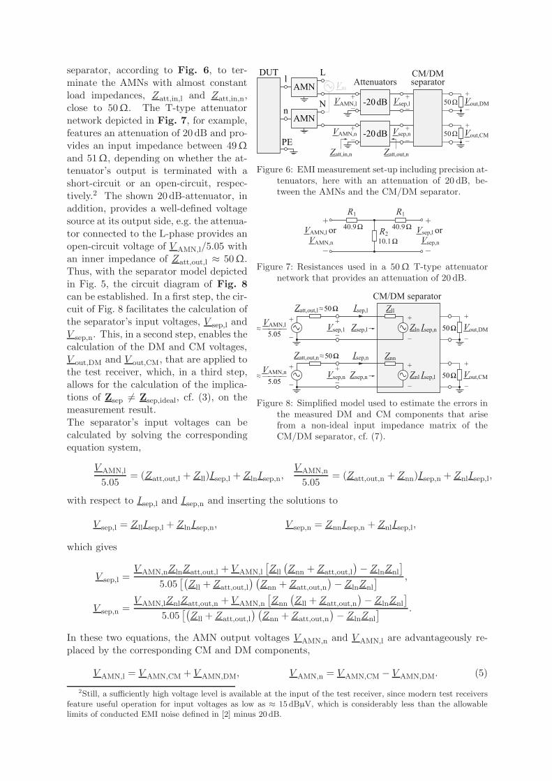
Figure 4: Measurement set-up employing a CM/DM sep-arator to directly provide the DM and CM compo-nents of the conducted EMI noise to a test receiver.
Initial measurements of conducted EMInoise often reveal insufficient filter atten-uation, in particular at high frequenciesabove 1MHz. In this context, the ques-tion arises how actual deficiencies of theEMI filter can be resolved in a systematicway. Since the EMI filter employs essen-tially different filter components to sup-press Differential Mode (DM) and Com-mon Mode (CM) EMI noise, a commonapproach for a diagnostic inspection is toseparate the conducted EMI noise intoDifferential Mode (DM) and CommonMode (CM) noise. Direct measurementof DM and CM EMI noise is feasible withthe measurement set-up depicted inFig. 4, which employs a CM/DM sep-arator and facilitates the measurementsof the conducted DM and CM EMI noisewithout and with EMI filter.With the results obtained from thesemeasurements it is possible to trace rea-sons for insufficient filter attenuations,cf. [3].A literature review reveals numer-ous different realizations of single-phaseCM/DM separators, which can be cate-gorized according to list below.
1. Passive separators suppress eitherDM or CM component and preservethe remaining CM or DM compo-nent, respectively. Examples areCM/DM separators realized withresistor networks [7] and separatorsthat employ broadband transformers [5–10].
2. Active separators employ operational amplifiers to determine DM and CM components [11,12].
3. Digital or software solutions, e.g. with the use of digital oscilloscopes [13,14].
4. Direct measurement of CM and DM components with current probes [15].
All CM/DM separators feature limited measurement accuracy, in particular due to limited CMand DM separation capabilities. In this context, the CM and DM transmission and rejectionratios (CMTR, DMTR, CMRR, and DMRR, cf. Section 1) are criteria used for evaluatingCM/DM separators [10]. In addition to limited separation capability of the separator itself,however, also interactions at the interfaces between the AMNs’ output ports and the separator’sinput ports in Fig. 4 may deteriorate the accuracy of the measured output voltages [16].This Paper evaluates the practicability of different CM/DM separators and, first, reveals com-mon properties of CM/DM separators in Section 1, i.e. input-side impedance characteristics
and CMTR, DMTR, CMRR, and DMRR values. Based on this summary the measurementerrors that result in a practical measurement set-up are estimated in Section 2. The definitionsgiven in Section 1 further facilitate the evaluation of a realized and improved version of an activeCM/DM separator circuit, originally proposed in [11,12], in Section 3, which uses operationalamplifiers and features competitive noise separation capability with DMTR/CMRR > 51 dBand CMTR/DMRR > 47 dB for frequencies up to 10MHz. Experimental results accompany thepresented investigations.
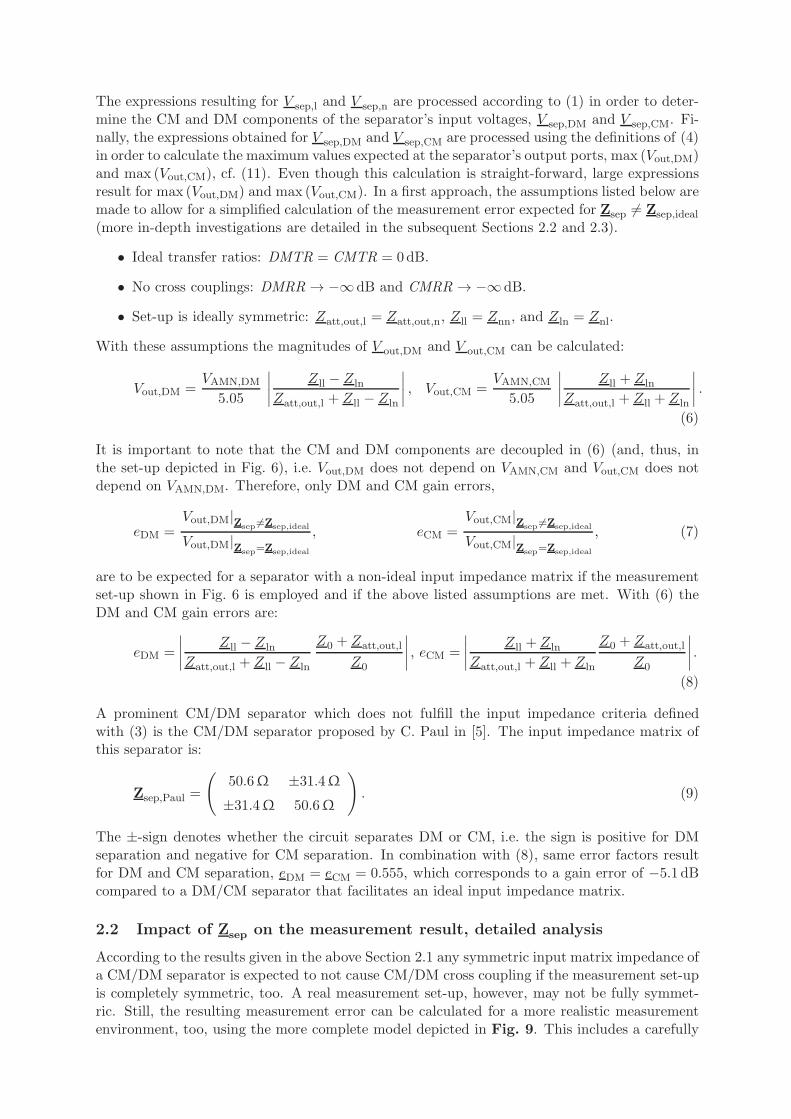
1 Properties of single-phase CM/DM separators
CM/DM separator
50 Ω
50 Ω Vout,DM
Vout,CM
Isep,l
Isep,n
Vsep,l
Vsep,n
Zll
Znn
Zln Isep,n
Znl Isep,l
Zsep,l
Zsep,n
Figure 5: Characterization of the input ports of aCM/DM separator based on impedance matrix co-efficients [16].
Any single-phase CM/DM separatorsenses two input voltages at its inputports, e.g. V sep,l and V sep,n in Fig. 5,and processes the measured voltages inorder to determine DM and CM compo-nents, which, in case of ideal separation,directly provides the values of the input-side DM and CM components,1
V sep,DM =V sep,l − V sep,n
2(1)
V sep,CM =V sep,l + V sep,n
2, (2)
at its output ports, i.e. V out,DM = V sep,DM and V out,CM = V sep,CM.In a practical realization the accuracy achievable for V out,DM and V out,CM is limited. This ispartly due to to an unsuitable input impedance matrix of the CM/DM separator,
Zsep =
(
Z ll Z ln
Znl Znn
)
6= Zsep,ideal =
(
50Ω 0
0 50Ω
)
, (3)
cf. Fig. 5, which introduces errors to V sep,l and V sep,n [16]. Further measurement errors arisefrom inaccurate processing of the measured voltages, commonly accounted for with gain errors[Differential Mode Transmission Ratio (DMTR) and / or Common Mode Transmission Ratio(CMTR) different to 0 dB] and cross coupling [Common Mode Rejection Ratio (CMRR) and /or Differential Mode Rejection Ratio (DMRR) greater than zero, i.e. greater than −∞dB].DMTR, CMTR, CMRR, and DMRR are defined according to [10]:
DMTR =
∣
∣
∣
∣
V out,DM
V sep,DM
∣
∣
∣
∣
, CMTR =
∣
∣
∣
∣
V out,CM
V sep,CM
∣
∣
∣
∣
, CMRR =
∣
∣
∣
∣
V out,DM
V sep,CM
∣
∣
∣
∣
, DMRR =
∣
∣
∣
∣
V out,CM
V sep,DM
∣
∣
∣
∣
. (4)
These four factors allow for the estimation of the maximum output voltages including gain errorsand cross coupling, which is detailed in Section 2.3.2.
2 Measurement errors in a practical set-up
2.1 Impact of Zsep on the measurement result, simplified analysis
Fig. 4 depicts the basic measurement set-up used to determine DM and CM EMI noise. Amore practical set-up, however, employs precision attenuators between the AMNs and the noise
1N.B.: In this document, variables with underlined capital letters denote phasors; V out,DM = Vout,DM ejϕout,DM ,for example, denotes the phasor of the DM output voltage with a RMS value of Vout,DM and a relative phaseangle equal to ϕout,DM, cf. [3].
AMN
AMN
-20 dB
-20 dBPE
Vout,CM50 Ω
50 Ω
VAMN,n
Zatt,in,n Zatt,out,n
VAMN,l Vsep,l
DUTl
n
L
N
Vsep,n
Vm
Vout,DM
CM/DMseparatorAttenuators
Figure 6: EMI measurement set-up including precision at-tenuators, here with an attenuation of 20 dB, be-tween the AMNs and the CM/DM separator.
Figure 7: Resistances used in a 50Ω T-type attenuatornetwork that provides an attenuation of 20 dB.
CM/DM separator
Isep,l Zll
Vsep,1 Zsep,l Zln Isep,n VAMN,l≈ ———— 5.05
Vout,DM50 Ω
Zatt,out,l ≈ 50 Ω
Isep,n Znn
Vsep,n Zsep,n Znl Isep,l VAMN,n≈ ———— 5.05
Vout,CM50 Ω
Zatt,out,n ≈ 50 Ω
Figure 8: Simplified model used to estimate the errors inthe measured DM and CM components that arisefrom a non-ideal input impedance matrix of theCM/DM separator, cf. (7).
separator, according to Fig. 6, to ter-minate the AMNs with almost constantload impedances, Zatt,in,l and Zatt,in,n,close to 50Ω. The T-type attenuatornetwork depicted in Fig. 7, for example,features an attenuation of 20 dB and pro-vides an input impedance between 49Ωand 51Ω, depending on whether the at-tenuator’s output is terminated with ashort-circuit or an open-circuit, respec-tively.2 The shown 20dB-attenuator, inaddition, provides a well-defined voltagesource at its output side, e.g. the attenua-tor connected to the L-phase provides anopen-circuit voltage of V AMN,l/5.05 withan inner impedance of Zatt,out,l ≈ 50Ω.Thus, with the separator model depictedin Fig. 5, the circuit diagram of Fig. 8can be established. In a first step, the cir-cuit of Fig. 8 facilitates the calculation ofthe separator’s input voltages, V sep,l andV sep,n. This, in a second step, enables thecalculation of the DM and CM voltages,V out,DM and V out,CM, that are applied tothe test receiver, which, in a third step,allows for the calculation of the implica-tions of Zsep 6= Zsep,ideal, cf. (3), on themeasurement result.The separator’s input voltages can becalculated by solving the correspondingequation system,
V AMN,l
5.05= (Zatt,out,l + Z ll)Isep,l + Z lnIsep,n,
V AMN,n
5.05= (Zatt,out,n + Znn)Isep,n + ZnlIsep,l,
with respect to Isep,l and Isep,n and inserting the solutions to
V sep,l = Z llIsep,l + Z lnIsep,n, V sep,n = ZnnIsep,n + ZnlIsep,l,
which gives
V sep,l =V AMN,nZ lnZatt,out,l + V AMN,l
[
Z ll
(
Znn + Zatt,out,l
)
− Z lnZnl
]
5.05[(
Z ll + Zatt,out,l
) (
Znn + Zatt,out,n
)
− Z lnZnl
] ,
V sep,n =V AMN,lZnlZatt,out,n + V AMN,n
[
Znn
(
Z ll + Zatt,out,n
)
− Z lnZnl
]
5.05[(
Z ll + Zatt,out,l
) (
Znn + Zatt,out,n
)
− Z lnZnl
] .
In these two equations, the AMN output voltages V AMN,n and V AMN,l are advantageously re-placed by the corresponding CM and DM components,
V AMN,l = V AMN,CM + V AMN,DM, V AMN,n = V AMN,CM − V AMN,DM. (5)
2Still, a sufficiently high voltage level is available at the input of the test receiver, since modern test receiversfeature useful operation for input voltages as low as ≈ 15 dBµV, which is considerably less than the allowablelimits of conducted EMI noise defined in [2] minus 20 dB.
The expressions resulting for V sep,l and V sep,n are processed according to (1) in order to deter-mine the CM and DM components of the separator’s input voltages, V sep,DM and V sep,CM. Fi-nally, the expressions obtained for V sep,DM and V sep,CM are processed using the definitions of (4)in order to calculate the maximum values expected at the separator’s output ports, max (Vout,DM)and max (Vout,CM), cf. (11). Even though this calculation is straight-forward, large expressionsresult for max (Vout,DM) and max (Vout,CM). In a first approach, the assumptions listed below aremade to allow for a simplified calculation of the measurement error expected for Zsep 6= Zsep,ideal
(more in-depth investigations are detailed in the subsequent Sections 2.2 and 2.3).
• Ideal transfer ratios: DMTR = CMTR = 0dB.
• No cross couplings: DMRR → −∞dB and CMRR → −∞dB.
• Set-up is ideally symmetric: Zatt,out,l = Zatt,out,n, Z ll = Znn, and Z ln = Znl.
With these assumptions the magnitudes of V out,DM and V out,CM can be calculated:
Vout,DM =VAMN,DM
5.05
∣
∣
∣
∣
Z ll − Z ln
Zatt,out,l + Z ll − Z ln
∣
∣
∣
∣
, Vout,CM =VAMN,CM
5.05
∣
∣
∣
∣
Z ll + Z ln
Zatt,out,l + Z ll + Z ln
∣
∣
∣
∣
.
(6)
It is important to note that the CM and DM components are decoupled in (6) (and, thus, inthe set-up depicted in Fig. 6), i.e. Vout,DM does not depend on VAMN,CM and Vout,CM does notdepend on VAMN,DM. Therefore, only DM and CM gain errors,
eDM =Vout,DM|
Zsep 6=Zsep,ideal
Vout,DM|Zsep=Zsep,ideal
, eCM =Vout,CM|
Zsep 6=Zsep,ideal
Vout,CM|Zsep=Zsep,ideal
, (7)
are to be expected for a separator with a non-ideal input impedance matrix if the measurementset-up shown in Fig. 6 is employed and if the above listed assumptions are met. With (6) theDM and CM gain errors are:
eDM =
∣
∣
∣
∣
Z ll − Z ln
Zatt,out,l + Z ll − Z ln
Z0 + Zatt,out,l
Z0
∣
∣
∣
∣
, eCM =
∣
∣
∣
∣
Z ll + Z ln
Zatt,out,l + Z ll + Z ln
Z0 + Zatt,out,l
Z0
∣
∣
∣
∣
.
(8)
A prominent CM/DM separator which does not fulfill the input impedance criteria definedwith (3) is the CM/DM separator proposed by C. Paul in [5]. The input impedance matrix ofthis separator is:
Zsep,Paul =
(
50.6Ω ±31.4Ω
±31.4Ω 50.6Ω
)
. (9)
The ±-sign denotes whether the circuit separates DM or CM, i.e. the sign is positive for DMseparation and negative for CM separation. In combination with (8), same error factors resultfor DM and CM separation, eDM = eCM = 0.555, which corresponds to a gain error of −5.1 dBcompared to a DM/CM separator that facilitates an ideal input impedance matrix.
2.2 Impact of Zsep on the measurement result, detailed analysis
According to the results given in the above Section 2.1 any symmetric input matrix impedance ofa CM/DM separator is expected to not cause CM/DM cross coupling if the measurement set-upis completely symmetric, too. A real measurement set-up, however, may not be fully symmet-ric. Still, the resulting measurement error can be calculated for a more realistic measurementenvironment, too, using the more complete model depicted in Fig. 9. This includes a carefully
−
+
−
+
−
+
−
+
−
++Vs,CM
−
+Vs,DM
−Zs,x
Zs,b
Zs,a
l
PE
Vsep,l
AMN
Vsep,n
CM/DM
separator
Vl AAMN
Attenuator
VAMN,l VAMN,n
AMNAttenuator
Aatt Aatt,rAsep AAMN,r−
+
PE
n
Vn
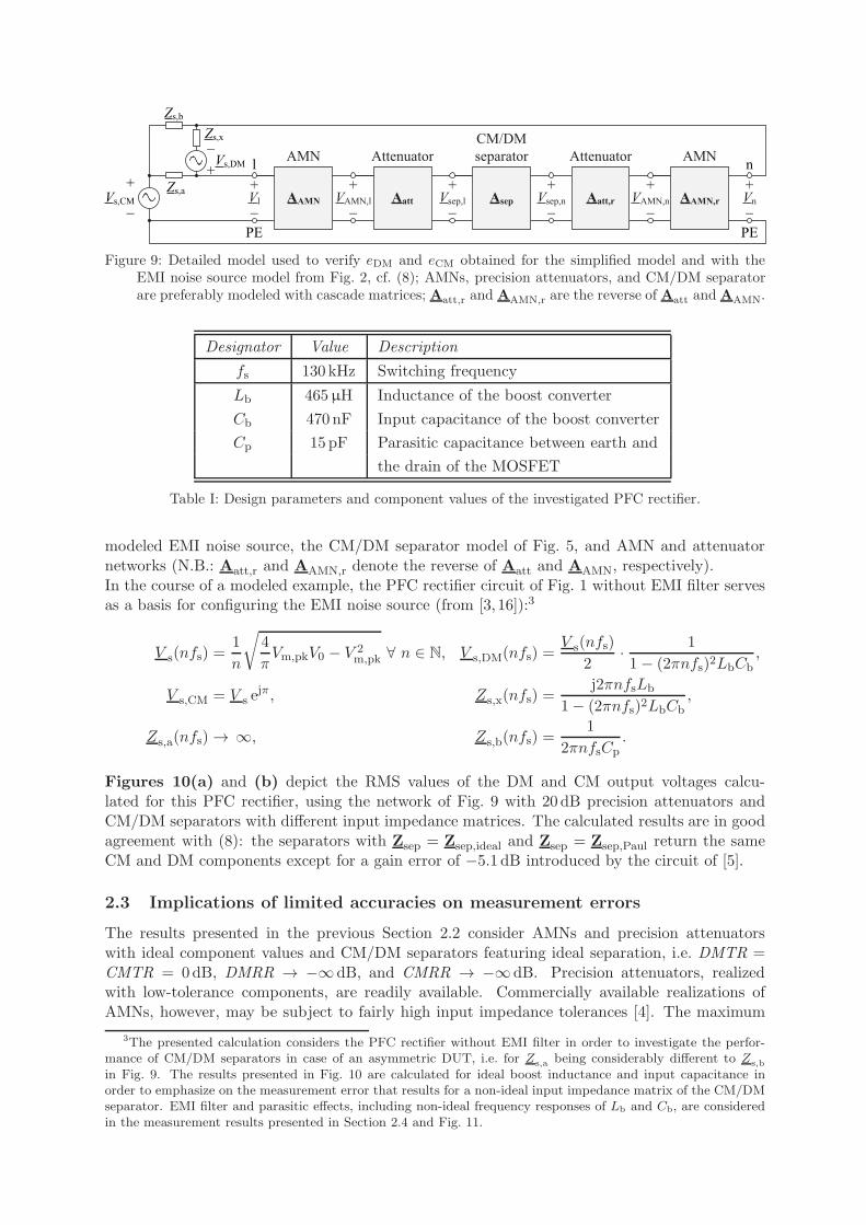
Figure 9: Detailed model used to verify eDM and eCM obtained for the simplified model and with theEMI noise source model from Fig. 2, cf. (8); AMNs, precision attenuators, and CM/DM separatorare preferably modeled with cascade matrices; Aatt,r and AAMN,r are the reverse of Aatt and AAMN.
Designator Value Description
fs 130 kHz Switching frequency
Lb 465µH Inductance of the boost converter
Cb 470 nF Input capacitance of the boost converter
Cp 15 pF Parasitic capacitance between earth and
the drain of the MOSFET
Table I: Design parameters and component values of the investigated PFC rectifier.
modeled EMI noise source, the CM/DM separator model of Fig. 5, and AMN and attenuatornetworks (N.B.: Aatt,r and AAMN,r denote the reverse of Aatt and AAMN, respectively).In the course of a modeled example, the PFC rectifier circuit of Fig. 1 without EMI filter servesas a basis for configuring the EMI noise source (from [3,16]):3
V s(nfs) =1
n
√
4
πVm,pkV0 − V 2
m,pk ∀ n ∈ N, V s,DM(nfs) =V s(nfs)
2·
1
1− (2πnfs)2LbCb
,
V s,CM = V s ejπ, Zs,x(nfs) =
j2πnfsLb
1− (2πnfs)2LbCb
,
Zs,a(nfs) → ∞, Zs,b(nfs) =1
2πnfsCp
.
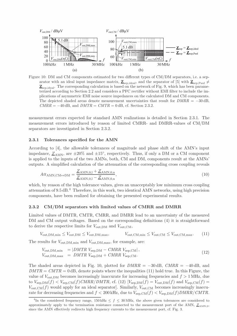
Figures 10(a) and (b) depict the RMS values of the DM and CM output voltages calcu-lated for this PFC rectifier, using the network of Fig. 9 with 20 dB precision attenuators andCM/DM separators with different input impedance matrices. The calculated results are in goodagreement with (8): the separators with Zsep = Zsep,ideal and Zsep = Zsep,Paul return the sameCM and DM components except for a gain error of −5.1 dB introduced by the circuit of [5].
2.3 Implications of limited accuracies on measurement errors
The results presented in the previous Section 2.2 consider AMNs and precision attenuatorswith ideal component values and CM/DM separators featuring ideal separation, i.e. DMTR =CMTR = 0dB, DMRR → −∞dB, and CMRR → −∞dB. Precision attenuators, realizedwith low-tolerance components, are readily available. Commercially available realizations ofAMNs, however, may be subject to fairly high input impedance tolerances [4]. The maximum
3The presented calculation considers the PFC rectifier without EMI filter in order to investigate the perfor-mance of CM/DM separators in case of an asymmetric DUT, i.e. for Zs,a being considerably different to Zs,b
in Fig. 9. The results presented in Fig. 10 are calculated for ideal boost inductance and input capacitance inorder to emphasize on the measurement error that results for a non-ideal input impedance matrix of the CM/DMseparator. EMI filter and parasitic effects, including non-ideal frequency responses of Lb and Cb, are consideredin the measurement results presented in Section 2.4 and Fig. 11.
Vout,DM / dBμV Vout,CM / dBμV
f
100
80
60
0
20
40
100 kHz 30 MHz1 MHz
f
100
80
60
100 kHz 30 MHz1 MHz
(a) (b)
5.1 dB
Vout,DM(nfs)
5.1 dB
Vout,CM(nfs)
Zsep = Zsep,ideal
Zsep = Zsep,Paul
Vout,DM,max
Vout,DM,minVout,CM,min
Vout,CM,max
Figure 10: DM and CM components estimated for two different types of CM/DM separators, i.e. a sep-arator with an ideal input impedance matrix, Zsep,ideal, and the separator of [5] with Zsep,Paul 6=Zsep,ideal. The corresponding calculation is based on the network of Fig. 9, which has been parame-terized according to Section 2.2 and considers a PFC rectifier without EMI filter to include the im-plications of asymmetric EMI noise source impedances on the calculated DM and CM components.The depicted shaded areas denote measurement uncertainties that result for DMRR = −30 dB,CMRR = −40 dB, and DMTR = CMTR = 0dB, cf. Section 2.3.2.
measurement errors expected for standard AMN realizations is detailed in Section 2.3.1. Themeasurement errors introduced by reason of limited CMRR- and DMRR-values of CM/DMseparators are investigated in Section 2.3.2.
2.3.1 Tolerances specified for the AMN
According to [4], the allowable tolerances of magnitude and phase shift of the AMN’s inputimpedance, ZAMN, are ±20% and ±15, respectively. Thus, if only a DM or a CM componentis applied to the inputs of the two AMNs, both, CM and DM, components result at the AMNs’outputs. A simplified calculation of the attenuation of the corresponding cross coupling reveals
AttAMN,CM↔DM =ZAMN,0,l + ZAMN,0,n
ZAMN,0,l − ZAMN,0,n
, (10)
which, by reason of the high tolerance values, gives an unacceptably low minimum cross couplingattenuation of 9.5 dB.4 Therefore, in this work, two identical AMN networks, using high precisioncomponents, have been realized for obtaining the presented experimental results.
2.3.2 CM/DM separators with limited values of CMRR and DMRR
Limited values of DMTR, CMTR, CMRR, and DMRR lead to an uncertainty of the measuredDM and CM output voltages. Based on the corresponding definitions (4) it is straightforwardto derive the respective limits for Vout,DM and Vout,CM,
Vout,DM,min ≤ Vout,DM ≤ Vout,DM,max, Vout,CM,min ≤ Vout,CM ≤ Vout,CM,max. (11)
The results for Vout,DM,min and Vout,DM,max, for example, are:
Vout,DM,min = |DMTR Vsep,DM − CMRR Vsep,CM| ,Vout,DM,max = DMTR Vsep,DM + CMRR Vsep,CM.
(12)
The shaded areas depicted in Fig. 10, plotted for DMRR = −30 dB, CMRR = −40 dB, andDMTR = CMTR = 0dB, denote points where the inequalities (11) hold true. In this Figure, thevalue of Vout,DM becomes increasingly inaccurate for increasing frequencies and f > 1MHz, dueto Vsep,DM(f) < Vsep,CM(f)CMRR/DMTR, cf. (12) [Vsep,DM(f) = Vout,DM(f) and Vsep,CM(f) =Vout,CM(f) would apply for an ideal separator]. Similarly, Vout,CM becomes increasingly inaccu-rate for decreasing frequencies and f < 200 kHz, due to Vsep,CM(f) < Vsep,DM(f)DMRR/CMTR.
4In the considered frequency range, 150 kHz ≤ f ≤ 30MHz, the above given tolerances are considered toapproximately apply to the termination resistance connected to the measurement port of the AMN, ZAMN,0,since the AMN effectively redirects high frequency currents to the measurement port, cf. Fig. 3.

(a) (b)
Figure 11: DM and CM components measured with two different types of CM/DM separators, i.e. aseparator with an ideal input impedance matrix, Zsep,ideal, and the separator of [5] with Zsep,Paul 6=Zsep,ideal, and with 20 dB precision attenuators. Thus, 20 dB need to be added to the depictedvalues in order to obtain the actual CM and DM components of the generated EMI noise. N.B.: again of 6dB is inherent to the CM/DM separator of [5] and has been removed by means of initialcalibration.
2.4 Comparison to measurement results
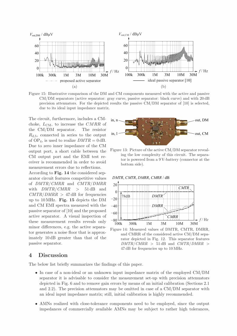
Figures 11(a) and (b) depict measured DM and CM components, which have been obtainedfor the considered PFC rectifier with EMI filters in order to avoid excessive high frequencyload of the AMNs. The separator proposed by C. Paul [5] again provides output voltages thatare approximately 5 dB below the output voltage measured with the separator proposed by S.Wang in [10], which features an input impedance matrix close to Zsep,ideal. The measurement,however, also includes additional errors in the higher frequency range, e.g. due to limited ratiosof DMTR/CMRR and CMTR/DMRR. Still, the difference of approximately 5 dB is clearlyapparent for DM and CM components.
3 Performance achieved with an active CM/DM separator
Figure 12: Schematic drawing of the presented activeCM/DM separator.
A successful realization of a passiveCM/DM separator includes careful opti-mization of broadband transformers andPCB layout in order to achieve accept-able separation capabilities in the re-quired wide frequency range between150 kHz and 30MHz. The CM/DM sep-arator, however, is subject to small sig-nal excitations, i.e. the AMNs keep thesupply currents away from it, a passiveCM/DM separator can be directly re-placed by an active realization, which al-lows for a straightforward implementa-tion with relatively low effort, i.e. thereis no need for cumbersome fine-tuning ofthe circuit.Fig. 12 depicts the circuit of the consid-ered active CM/DM separator, Fig. 13 depicts a picture of the realized device. It employs fouroperational amplifiers: OP1 and OP2 realize an ideal input impedance matrix [together withRin,l and Rin,n, cf. (3)], and OP3 and OP4 determine the CM and DM voltages, respectively.Adequate operational amplifiers (in the presented circuit four AD8051 are used) and close-tolerance resistors need to be employed in order to achieve high CM/DM separation capability.
out,DM
(a)
[10]
(b)
Figure 15: Illustrative comparison of the DM and CM components measured with the active and passiveCM/DM separators (active separator: gray curve, passive separator: black curve) and with 20 dBprecision attenuators. For the depicted results the passive CM/DM separator of [10] is selected,due to its ideal input impedance matrix.
in, n
in, l
out, DM
out, CM
Figure 13: Picture of the active CM/DM separator reveal-ing the low complexity of this circuit. The separa-tor is powered from a 9V-battery (connector at thebottom side).
CMRR
DMTR, CMTR, DMRR, CMRR / dB
DMTR
DMRR
CMTR
Figure 14: Measured values of DMTR, CMTR, DMRR,and CMRR of the considered active CM/DM sepa-rator depicted in Fig. 12. This separator featuresDMTR/CMRR > 51 dB and CMTR/DMRR >47 dB for frequencies up to 10MHz.
The circuit, furthermore, includes a CM-choke, LCM, to increase the CMRR ofthe CM/DM separator. The resistorRd,5, connected in series to the outputof OP4, is used to realize DMTR = 0dB.Due to zero inner impedance of the CMoutput port, a short cable between theCM output port and the EMI test re-ceiver is recommended in order to avoidmeasurement errors due to reflections.According to Fig. 14 the considered sep-arator circuit features competitive valuesof DMTR/CMRR and CMTR/DMRR
with DMTR/CMRR > 51 dB andCMTR/DMRR > 47 dB for frequenciesup to 10MHz. Fig. 15 depicts the DMand CM EMI spectra measured with thepassive separator of [10] and the proposedactive separator. A visual inspection ofthese measurement results reveals onlyminor differences, e.g. the active separa-tor generates a noise floor that is approx-imately 10 dB greater than that of thepassive separator.
4 Discussion
The below list briefly summarizes the findings of this paper.
• In case of a non-ideal or an unknown input impedance matrix of the employed CM/DMseparator it is advisable to consider the measurement set-up with precision attenuatorsdepicted in Fig. 6 and to remove gain errors by means of an initial calibration (Sections 2.1and 2.2). The precision attenuators may be omitted in case of a CM/DM separator withan ideal input impedance matrix; still, initial calibration is highly recommended.
• AMNs realized with close-tolerance components need to be employed, since the outputimpedances of commercially available AMNs may be subject to rather high tolerances,
which considerably deteriorates the measurement results (Section 2.3.1).
• The value of the DM output signal is inaccurate if Vsep,DM(f) < Vsep,CM(f)CMRR/DMTR
applies, i.e. in presence of a comparably high CM input signal. The value of the CM outputsignal is inaccurate if Vsep,DM(f) < Vsep,CM(f)CMRR/DMTR applies, i.e. in presence of acomparably high DM input signal (Section 2.3.2).
5 Conclusion
Two contributions to the practical measurement of CM and DM components of conducted EMIare detailed. First, the implications of the impedance criterion given with (3) on the measure-ment errors are investigated. Analytical results obtained for a simplified model are verified bymeans of a more detailed model of the considered measurement set-up and experimental results.According to the obtained results, only a gain error is expected with the considered measure-ment configuration, which can be removed by initial calibration. Second, an active CM/DMseparator is detailed, which features straightforward realization and competitive separation ca-pability, DMTR/CMRR > 51 dB and CMTR/DMRR > 47 dB for frequencies up to 10MHz. Agood matching of EMI spectra measured with passive and active separators is presented.
References
[1] IEC 61000-3-2: Electromagnetic compatibility (EMC) – Part 3 Limits, Section 2: Limits for har-monic current emissions (equipment input current 16 A per phase), 2005.
[2] IEC 61000-6-3: Electromagnetic compatibility (EMC) – Part 6 Generic standards, Section 3: Emis-sion standard for residential, commercial and light-industrial environments, 2006.
[3] I. Kovacevic, F. Krismer, S. Schroth, and J. W. Kolar: “Practical characterization of EMI filtersreplacing CISPR 17 approximate worst case measurements,” Proc. of the IEEE 14th COMPEL 2013,10 pp., June 2013.
[4] IEC/CISPR 16-1-2 Specification for radio disturbance and immunity measuring apparatus and meth-ods – Part 1: Radio disturbance and immunity measuring apparatus, Section 2: Ancillary equipment– Conducted disturbances, 2003.
[5] C. Paul and K. B Hardin, “Diagnosis and reduction of conducted noise emmisions,” IEEE Trans-
action on Electromagnetic Compatibility, vol. 30, no. 4, pp. 553–560, Nov. 1988.[6] K.Y. See, “Network for conducted EMI diagnosis,” Electronic Letters, vol. 35, no. 17, pp. 1446–1447,
Aug. 1999.[7] M. J. Nave, “A novel differential mode rejection network for conducted emissions diagnostics,” IEEE
National Symposium on Electromagnetic Compatibility 1989, pp. 223–227, May 1989.[8] T. Guo, D.Y. Chen, and F.C. Lee, “Separation of the common-mode- and differential-mode-
conducted EMI noise,” IEEE Transaction on Power Electronics, vol. 11, no. 3, pp. 480–488,May 1996.
[9] A. Nagel and R. W. De Doncker, “Separating common mode and differential mode noise in EMImeasurements,” Proc. of the 8th EPE 1999, 8 pp., Sept. 1999.
[10] S. Wang, F. C. Lee, and W. G. Odendaal, “Characterization, evaluation, and design of noise sepa-rator for conducted EMI noise diagnosis,” IEEE Transaction on Power Electronics, vol. 20, no. 4,pp. 974–982, July 2005.
[11] T. von Rauner, “A measurement system for evaluatiom of the coupling modes and mechanisms ofconductive noise,” Master’s thesis, Electrical and Communications Engineering, Helsinki Universityof Technology, June 1999.
[12] P.-S. Chen, “Software-based separation of conductive EMI signals,” Proc. of the IEEE 10th
IAS 2006, vol. 3, pp. 1209–1214, Oct. 2006.[13] J. Kelin, W. Jingmei, W. Chang, and B. Chuang, “A new method for conducted EMI noise diagno-
sis,” Proc. of the IEEE 8th ICEMI 2007, pp. 4-59–4-63, Aug. 2007.[14] Y.-K. Lo, H.-J. Chiu, T.-H. Song, M.-P. Chen, and T.-S. Luor, “A software-based CM and DM
measurement system for the conducted EMI,” Proc. of the IEEE 25th IECON 1999, vol. 1, pp. 253–255, Nov./Dec. 1999.
[15] J. Stahl, D. Kuebrich, and T. Duerbaum, “Modification and characterization of a standard LISNfor effective EMI noise separation,” Proc. of the IEEE 12th ICEAA 2010, pp. 39–42, Sept. 2010.
[16] K. S. Kostov, H.-P. Nee, M. Priecinsky, “The input impedance of common mode and differentialmode noise separators,” Proc. of the IEEE 5th ECCE 2013, pp. 1688–1695, Sept. 2013.


![Time DomainMeasurement System EMI and CM/DM … · to lower the generation of conducted EMI, the R&Dpeople is getting more and ... [1]. In this study, the Front Panel including theof](https://img.pdfslide.net/doc/110x75/5ad6fd197f8b9a5b538c0e5a/time-domainmeasurement-system-emi-and-cmdm-lower-the-generation-of-conducted.jpg)