Embed Size (px)
Citation preview
Annual Report 2001
Solid-State Electronics Department Prof.Dr.rer.nat. F.J.Tegude
Gerhard-Mercator-Universität Duisburg Fakultät für Ingenieurwissenschaften
Institut für Technologien der Informationstechnik
Halbleitertechnik/Halbleitertechnologie
Lotharstrasse 55 / ZHO D-47057 Duisburg
Germany
Tel.: ++49 (0)203 379 3392 (Secr.) Fax: ++49 (0)203 379 3400 email: [email protected] www: http://www.zho.uni-duisburg.de
Editor: Dr.-Ing. Wolfgang Brockerhoff
Gerhard - MercatorUniversität Duisburg Halbleitertechnik/
Halbleitertechnologie

Annual Report 2001 - Solid-State Electronics Department
Table of Contents 1 Preface ................................................................................................................................. 1
2 Members of the Department ...................................................................................................... 3
3 Teaching Activities..................................................................................................................... 5 3.1 Lectures and Laboratory Exercises ............................................................................................ 5 3.2 Student Reports and Diploma Thesis (Studien-/Diplomarbeiten).............................................. 8 3.3 Doctor Thesis.............................................................................................................................. 8 3.4 Seminar on Semiconductor Electronics...................................................................................... 9
4 Research Activities .................................................................................................................. 11 4.1 Materials, Growth and Characterization............................................................................. 11
4.1.1 MOVPE Growth and Polarisation Dependence of (dis-)ordered InGaAsP PIN diodes for Optical Fibre Applications
S. Neumann, J. Spieler1), R. Blache1) .................................................................... 12 1): Technische Physik I, G. H. Döhler, University Erlangen-Nürnberg
4.1.2 Growth of Carbon doped InAlAs with LP-MOVPE and Non Gaseous Sources S. Neumann, M. Haase .......................................................................................... 15
4.1.3 Growth of III/V Resonant Tunnelling Diode on Si Substrate with LP-MOVPE S. Neumann, A. Bakin1), A. Osinski 1): Institut für Halbleitertechnik, A. Schlachetzki, TU Braunschweig ..................................... 18
4.1.4 Investigation of Different Composite-Collector Designs in In0.53Ga0.47As/InP DHBTs T. Reimann, S. Neumann, P. Velling (Innovative Processing AG, Duisburg), A. Osinski, M. Haase.................................................................................................. 21
4.1.5 Growth and Thermal Desorption of the Thin As Layer for Temporary Passivation of a Semiconductor Surface
V. Khorenko, W. Prost, R. Geitmann..................................................................... 24 4.2 Device and Circuit Simulation, Measurement and Modeling .......................................... 27
4.2.1 A Consistent PSPICE Model for InP based HBT S. Ehrich ............................................................................................................... 28
4.2.2 RF-Simulations of InGaP/GaAs Heterojunction Bipolar Transistors B. Schlothmann , S. Ehrich, M. Agethen, P. Velling.............................................. 31
4.2.3 Development of a Calibration Procedure for High-speed Time Domain Measurements
T. Gernandt,H. van Husen..................................................................................... 35
4.2.4 Design, Build-Up and Testing of a Full Digital Controller for DC/DC-Converters J. Driesen, R.M. Bertenburg.................................................................................. 38
4.2.5 Automated Wafer Probing O. El Alami, M. Agethen, S. Ehrich....................................................................... 42

Annual Report 2001 - Solid-State Electronics Department
4.3 Device and Circuit Processing and Characterization ....................................................... 45
4.3.1 Lithographic Tools for Laterally Controlled Nanocrystal Deposition F. Otten.................................................................................................................. 46
4.3.2 Integration of HBTs with Electroabsorption Waveguide Modulators and Applications T. Reimann, S. Neumann, H. van Husen, M. Schneider, A. Stöhr, M. Haase........ 49
4.3.3 Fabrication and Characterisation of Metamorphic InP/InGaAs HBTs Grown on GaAs Substrate
S-O. Kim, S. Ehrich ............................................................................................... 52
4.3.4 Design and Fabrication of RTD/HBT NOR Gate Grown by MOVPE/MBE Hybride Epitaxy
S-O. Kim, P. Glösekötter ...................................................................................... 55
4.3.5 The ELPHY SCRIPT GENERATOR: new tool to translate layout datas into machine control statement for an electron beam direct writing system
J. Degenhardt ........................................................................................................ 58
4.3.6 Development of a Control Program for the Leybold Vacuum Coating Plant Model L560
J. Driesen, R.M.Bertenburg................................................................................... 63 4.4 Conference Contributions......................................................................................................... 67 4.5 Publications ............................................................................................................................. 70 4.6 Research Projects ..................................................................................................................... 73
5 Guide to the Solid-State Electronics Department .................................................................... 74

Annual Report 2001 - Solid-State Electronics Department 1
1 Preface
For our Gerhard-Mercator-University 2001 continued to be characterized by reorganization. The former Faculty of Electrical Engineering and Information Technology has now been integrated into the Faculty of Engineering Science, containing also the divisions of Mechanical Engineering and Material Science. Further, negotiations are being conducted to strongly cooperate or even merge with the University of Essen, which is situated very near to Duisburg.
This report again presents the teaching and research activities of the Solid State Electronics Department (Fachgebiet Halbleitertechnik/Halbleitertechnolgie) during the year 2001.
As in recent years, our work concentrated on III-V materials, devices and circuits, based on Indium Phosphide (InP), mainly. After the maturing of research on single Heterostructure Fieldeffect-Transistors (HFET), even on InP, main emphasis has been put on Heterostructure Bipolar Transistors (HBT). Device combinations with enhanced functionality, like HBT merged with Resonant Tunnelling Diodes (RTD), and HBT / Electro-Optical Absorption Modulators, have been developed and investigated thoroughly.
The success of our work can be expressed by new major funding within three projects of the EU, within the Sonderforschungsbereich 445 “Nano-Particles From the Gas Phase”, and within a special program of our university on “New Technologies for Signal Demodulation” , which are conducted in addition to single projects funded by the DFG, BMBF and different industry partners.
Our HFET activities concentrate on design, fabrication and modelling of digital circuits, with a complexity of several hundred transistor functions on a chip. Besides fundamental activities on single HBT, like MOVPE layer growth with alternative sources, device processing, rf- and noise characterization as well as simulation and modelling, we started to fabricate HBT circuits. Special progress has been achieved on RTD/HBT digital circuits.
We appreciate a continuing increase of candidates for Diploma and PhD theses, which, after the strong decrease in recent years, is a very important and positive development for us. This clearly originates from the enhanced attractiveness of our department due to the excellent research facilities of our department.
Finally, I want to thank all friends and partners for cooperation and support, and especially all members and students of the department for their efforts and contributions to this report.
Duisburg, April 2002
Prof. Dr.rer.nat. F.J.Tegude

2 Annual Report 2001 - Solid-State Electronics Department
2
Annual Report 2001 - Solid-State Electronics Department 3
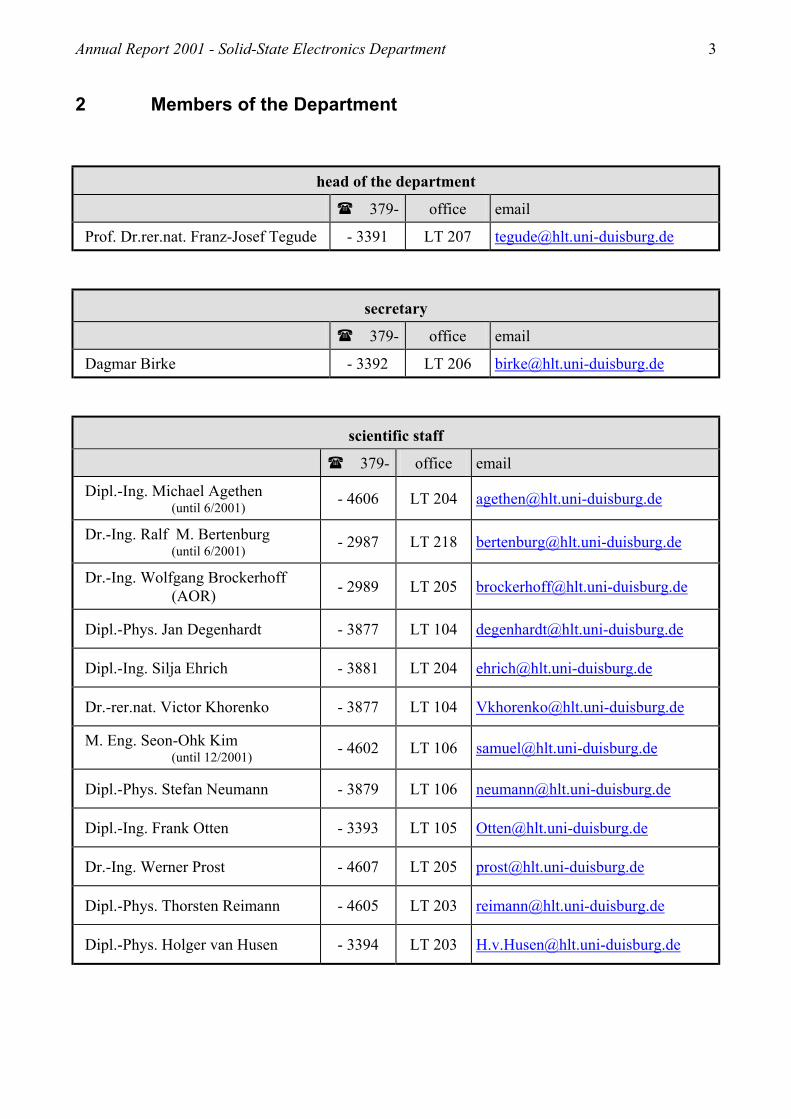
2 Members of the Department
head of the department
379- office email
Prof. Dr.rer.nat. Franz-Josef Tegude - 3391 LT 207 [email protected]
secretary
379- office email
Dagmar Birke - 3392 LT 206 [email protected]
scientific staff
379- office email
Dipl.-Ing. Michael Agethen (until 6/2001) - 4606 LT 204 [email protected]
Dr.-Ing. Ralf M. Bertenburg (until 6/2001) - 2987 LT 218 [email protected]
Dr.-Ing. Wolfgang Brockerhoff (AOR) - 2989 LT 205 [email protected]
Dipl.-Phys. Jan Degenhardt - 3877 LT 104 [email protected]
Dipl.-Ing. Silja Ehrich - 3881 LT 204 [email protected]
Dr.-rer.nat. Victor Khorenko - 3877 LT 104 [email protected]
M. Eng. Seon-Ohk Kim (until 12/2001) - 4602 LT 106 [email protected]
Dipl.-Phys. Stefan Neumann - 3879 LT 106 [email protected]
Dipl.-Ing. Frank Otten - 3393 LT 105 [email protected]
Dr.-Ing. Werner Prost - 4607 LT 205 [email protected]
Dipl.-Phys. Thorsten Reimann - 4605 LT 203 [email protected]
Dipl.-Phys. Holger van Husen - 3394 LT 203 [email protected]

4 Annual Report 2001 - Solid-State Electronics Department
technical staff
379- office email
Udo Doerk - 3395 LT 202 [email protected]
Dipl.-Ing. Ralf Geitmann - 4604 LT 202 [email protected]
Dipl.-Ing. Matthias Haase - 4602 LT 106 [email protected]
Dipl.-Ing. Wolfgang Molls - 4603 LT 201 [email protected]
Andrea Osinski - 4600 LT 104 [email protected]
Sabine Schwartz - 4601 LT 105 [email protected]
Ing. (grad.) Reimund Tilders - 3396 LT 201 [email protected]
Claudia Schmidt - 4095 LT 106 [email protected]
Jana Bödige - 4618 LT 106 [email protected]
students Gurujai Bagepalli Giuseppe Landi Matthias Barth Andreas Matiss Kartsen Bettray Mohana Reddy Sadan Celik Markus Menzel Adam Chwalczyk Augustine Che Mofor Serge Deragopian Artur Poloczek Quoc Thai Do Ingo Regolin Jörn Driesen Pyla Satya Sai Sridhar Ouafa El Alami Thorsten Scholz Tassilo Gernandt Michael Tekloth Urs Heidemann Conny Walzebug Raju Joy
guests Prof.Dr. Pinaki-Mazumder University of Michigan
Dr. Knut Deppert Lund University

Annual Report 2001 - Solid-State Electronics Department 5
3 Teaching Activities 3.1 Lectures and Laboratory Exercises
Lectures and exercises Schedule
Solid-State Electronics 1,2 (Festkörperelektronik 1,2)
3rd and 4th semester
Field Effect Electronics (Technische Elektronik 1)
5th semester
Bipolar Transistors and Circuits (Technische Elektronik 2)
6th semester
Semiconductor Microelectronics Technology 1,2 (Halbleitertechnologie 1,2) 7th and 8th semester
Fundamentals of Electronic Devices and Circuits (Grundlagen elektronischer Bauelmente und Schaltungen)
3rd semester / AOS
Basic Electronic Devices and Circuits 6th semester / AOS
III-V Technologies and Components 1/ Semiconductor Technology 1 (Halbleitertechnologie 1)
5th semester
Laboratory exercises
Communication Electronics (Praktikum Technische Elektronik und Hochfrequenztechnik)
7th semester
Introduction to Operational Amplifiers (Operationsverstärker-Praktikum)
6th semester
Semiconductor Technology 2 (Halbleitertechnologie 2)
8th semester
Seminars and Colloquia
Seminar on Semiconductor Electronics (Probleme der modernen Halbleiterphysik)
Seminar on Epitaxial Problems
Colloquium on Optoelectronics (together with other departments)
6 Annual Report 2001 - Solid-State Electronics Department
6
Lectures and Exercises:
Introduction to Solid-State Electronics / Solid-State Electronics 1,2 (Einführung in die Festkörperelektronik) / (Festkörperelektronik 1,2)
These courses start with an introduction to the basics of Quantum physics. Based on Schroedinger's equation and Heisenberg's uncertainty relations a comprehensive understanding of semiconductor band structure is achieved. The first part (Introduction to Solid-State Electronics) also includes carrier statistics and ends up with a discussion of current continuity and Poisson's equation. In the second part of this lecture the basic building blocks of electronic devices, i.e. semiconductor-metal contact, MIS system, pn junction and heterostructures, are treated for subsequent courses on field effect and bipolar electronics.
Field Effect Electronics (Technische Elektronik 1)
The main topic of this course are the MOS-devices and circuits. Starting with the basics concerning MOS-capacitors and charge-coupled devices, the fundamentals of field-effect transistors (MOSFET, MESFET, JFET) are treated. The basic methods to calculate complex electronic circuits are covered and applied to numerous analog and digital circuits.
Bipolar Transistors and Circuits (Technische Elektronik 2)
This course covers aspects of bipolar devices including an overview about special devices like tunneling and zener diodes. The DC- and AC-behaviour of pn-diodes and bipolar transistors is intensively studied resulting in a discussion of various small-signal equivalent circuits. In the second part fundamental integrated analog (e.g. operational amplifiers) and digital circuits are analysed and discussed.
Semiconductor Microelectronics Technology 1,2 (Halbleitertechnologie 1,2)
The semiconductor microelectronics technology lectures are devoted to III/V-semiconductor heterostructures for high speed electronic devices. The process steps from crystal growth to circuit fabrication are discussed. The first semester is focused on heterostructure material issues. Modern growth techniques like molecular beam epitaxy (MBE) and metal-organic vapour-phase epitaxy (MOVPE) are discussed in terms atomic layer control of thickness, composition, and doping. High Resolution X-ray diffraction, photoluminescence, and ellipsometry are explained for non-destructive material assessment in the mono-layer scale. The second semester is devoted to microelectronic fabrication techniques for high speed (f ≥100 GHz) devices and circuits. The lateral and vertical processing of epitaxial films, insulating layers, and metallizations are presented for high performance monolithic high speed analog and digital integrated circuits.
Annual Report 2001 - Solid-State Electronics Department 7
Laboratory exercises
Communication Electronics (Praktikum Technische Elektronik und Hochfrequenztechnik)
Within the laboratory exercises students apply their theoretical knowledge based on the lectures "Field Effect Electronics" and "Bipolar Transistors and Circuits". The capacitance-voltage charac-teristics of schottky diodes are measured and evaluated. The switching behaviour of bipolar transistors is experimentally investigated as well as the dynamical performance of digital circuits. Additionally, numerical simulation and synthesis of basic electronic circuits are carried out on a UNIX system.
Introduction to Operational Amplifiers (Operationsverstärker-Praktikum)
The aim of this course is the understanding of the basic principles and the characteristics of operational amplifiers (OpAmps). The laboratory exercises demonstrate their applicability in electronic circuits enabling the students to an independent design and understanding of complex circuits. Starting with the measurement and interpretation of the most important characteristic parameters of OpAmps, circuits like adders and multipliers, amplifiers and active filters are intensively calculated and investigated. Oscillators and generators are designed and measured.
Seminars and Colloquia
Seminar on Semiconductor Electronics (Probleme der modernen Halbleiterphysik)
Within this seminar modern topics of the semiconductor electronics are discussed and students, but also members of the department, report about their own work, e.g. the diploma thesis.
Seminar on Epitaxial Problems
Problems of the epitaxial growth of semiconductor structures are analysed, results are interpreted and future trends are discussed.
Colloquium on Optoelectronics Recent developments and problems in the Optoelectronics/Photonics field and neighboured topics are presented by invited experts from all over the world.

8 Annual Report 2001 - Solid-State Electronics Department
3.2 Student Reports and Diploma Thesis (Studien-/Diplomarbeiten)
Student reports
DRIESEN, JÖRN
Entwicklung eines Programmes zur Aufdampfsteuerung eines Leybold Pumpstands L560 February 2001
GERNANDT, TASSILO Entwicklung eines Kalibrierverfahrens für die Hochgeschwindigkeits-Zeitbereichsmesstechnik
July 2001
EL-ALAMI, OUAFA Entwicklung eines Agilent-VEE Programms zur Ansteuerung eines halbautomatischen DC-Messplatzes August 2001
Diploma thesis
DRIESEN, JÖRN Entwicklung, Aufbau und Erprobung einer vollständig digitalen Regelung für Gleichspannungswandler November 2001
3.3 Doctor Thesis
PASSENBERG, WOLFGANG Überwachsen strukturierter Epitaxieschichten mit der Molekularstrahl-Epitaxie zur Herstellung opto-elektronischer integrierter Schaltkreise October 2001

Annual Report 2001 - Solid-State Electronics Department 9
3.4 Seminar on Semiconductor Electronics 18.01.2001 B. SCHLOTHMANN, , report on the diploma work:
Zweidimensiona le physikalische Simulation von InP-HBT mit TCAD 24.04.2001 J.DRIESEN, , report on the student work:
"Entwicklung eines Programmes zur Aufdampfsteuerung eines Leybold Pumpstands L560"
07.06.2001 S.SCHÜLLER, Bericht über die Tagung:
"11th Conference and Exhibtion on Microwaves and Radio Communication"
21.06.2001 F.J.TEGUDE, report on: "Workshop on Compound Semiconductor Devices and Circuits" ( WOCSDICE
2001), Italy
J.DEGENHARDT, report on:the project:
"Logic Circuits with Reduced Complexity based on Devices with Higher Functionality"
28.06.2001 T.REIMANN, S.NEUMANN, Stand der Arbeiten im Projekt "Wellenleiter-Modulatoren"
05.07.2001 M.AGETHEN, report on: "IEEE Int. Microwave Symposium" ( MTT-S), USA M.AGETHEN, Stand der Arbeiten im Projekt
"Hochlinearisierte Sendeverstärker"
12.07.2001 T. GERNANDT, report on the student work: "Fehlermodell für den Zeitbereichsmessplatz"
15.11.2001 W. PROST, report on: '13th Int. Conf. on InP and Related Materials ( IPRM'01), Nara, Japan, 14.05.01-
18.05.01' F.J. TEGUDE, report on: '31st European Microwave Conference ( EuMC'2001), London, U.K., 25.09.01-
27.09.01'
22.11.2001 O. EL-ALAMI, report on the student work: 'Entwicklung eines Agilent-VEE Programms zur Ansteuerung eines
halbautomatischen DC-Messplatzes'
29.11.2001 B. SCHLOTHMANN, report on: 'Physikalische Simulation von InP basierenden Heterostrukturbipolartransistoren
(HBT)' - Stand der Arbeiten

10 Annual Report 2001 - Solid-State Electronics Department
06.12.2001 M. AGETHEN, report on:
'27th European Conference on Optical Communication ( ECOC '01), Amsterdam, The Netherlands, 30.09.01-04.10.01'
S. EHRICH, report on: 'Rauschmessungen für die Kommunikationstechnik ( 2001), Kamp-Lintfort,
Germany, 23.10.01-24.10.01'
13.12.2001 J. DRIESEN, report on the diploma thesis: 'Entwicklung, Aufbau und Erprobung einer vollständig digitalen Regelung für
Gleichspannungswandler'
20.12.2001 W. PROST, V. KHORENKO, report on: 'Nanopartikel in Heterostrukturschichten''

Annual Report 2001 - Solid-State Electronics Department 11
4 Research Activities
4.1 Materials, Growth and Characterization
12 Annual Report 2001 - Solid-State Electronics Department
4.1.1 MOVPE Growth and Polarisation Dependence of (dis-)ordered InGaAsP PIN Diodes for Optical Fibre Applications
Scientist: S. Neumann, J. Spieler1)
Student: Robert Blache1)
1): Technische Physik I, G. H. Döhler, University Erlangen-Nürnberg
Background
The polarisation mode dispersion (PMD) is limiting the transmission capacity of conventional multi-mode optical fibre [e.g. 1]. The on-line correction of PMD may become feasible if a dynamic polarisation dispersion measurement could trigger a PMD correction circuitry [1]. The near band-gap absorption anisotropy of ordered semiconductor layers is proposed here for polarisation measurement. Microelectronic polarisation dependent devices could be of considerable interest for PMD compensation if their wavelength of operation could be transferred to the wavelength of the optical fibre.
In this work a polarisation anisotropy of ordered InGaAsP layers adopted to the optical fibre wavelength regime of 1.3 µm and 1.55 µm is demonstrated and first polarisation dependent devices are presented.
Approach
Some MOVPE grown III/V ternary and quaternary layers exhibit under certain growth conditions a natural superlattice of binary monolayers along the [111]B direction. In ordered layers the degeneracy of the valence band is reversed and an energy splitting between light and heavy hole valence band ∆EVBS occurs [2-5]. Moreover, due to selection rules the absorption of polarised light with an energy close to the band-gap becomes dependent on the crystal orientation. It is well known that the ternary layers InGaAs on InP-substrate and GaInP on GaAs-substrate exhibit a high degree of group-III ordering [2-4]. An optical anisotropy was also achieved using In.64Ga.36As.12P.88 layers on GaAs-substrates [5] resulting in a low wavelength of ~ 700 nm.
A suitable candidate for the desired wavelength regime, however, is an In1-xGaxAs1-yPy absorption layer lattice matched to InP. The specific need of ordering is here a low growth temperature (Tg = 520 – 575 °C). Using the standard hydrides as group-V sources this temperature is below the diffusion controlled growth regime and results in unstable growth conditions. Therefore, we have used liquid group-V precursors (TBAs, TBP). Especially the better thermal decomposition of TBP compared to PH3 is a key component to realise a constant phosphorous content y during growth of even thick In1-xGaxAs1-yPy layers. This way the exploitation of the ordering effect of thick and lattice matched In1-xGaxAs1-yPy layers is feasible for various wavelengths including 1.3 µm and 1.55 µm.
Annual Report 2001 - Solid-State Electronics Department 13
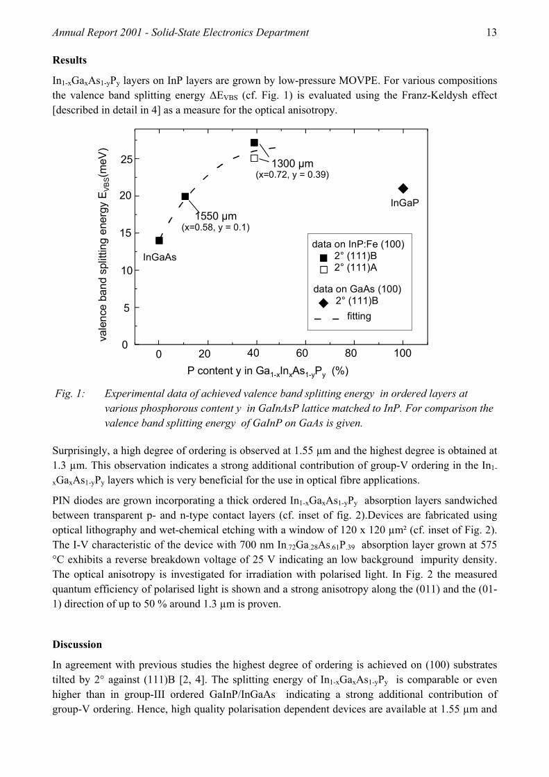
Results
In1-xGaxAs1-yPy layers on InP layers are grown by low-pressure MOVPE. For various compositions the valence band splitting energy ∆EVBS (cf. Fig. 1) is evaluated using the Franz-Keldysh effect [described in detail in 4] as a measure for the optical anisotropy.
Fig. 1: Experimental data of achieved valence band splitting energy in ordered layers at various phosphorous content y in GaInAsP lattice matched to InP. For comparison the valence band splitting energy of GaInP on GaAs is given.
Surprisingly, a high degree of ordering is observed at 1.55 µm and the highest degree is obtained at 1.3 µm. This observation indicates a strong additional contribution of group-V ordering in the In1-
xGaxAs1-yPy layers which is very beneficial for the use in optical fibre applications.
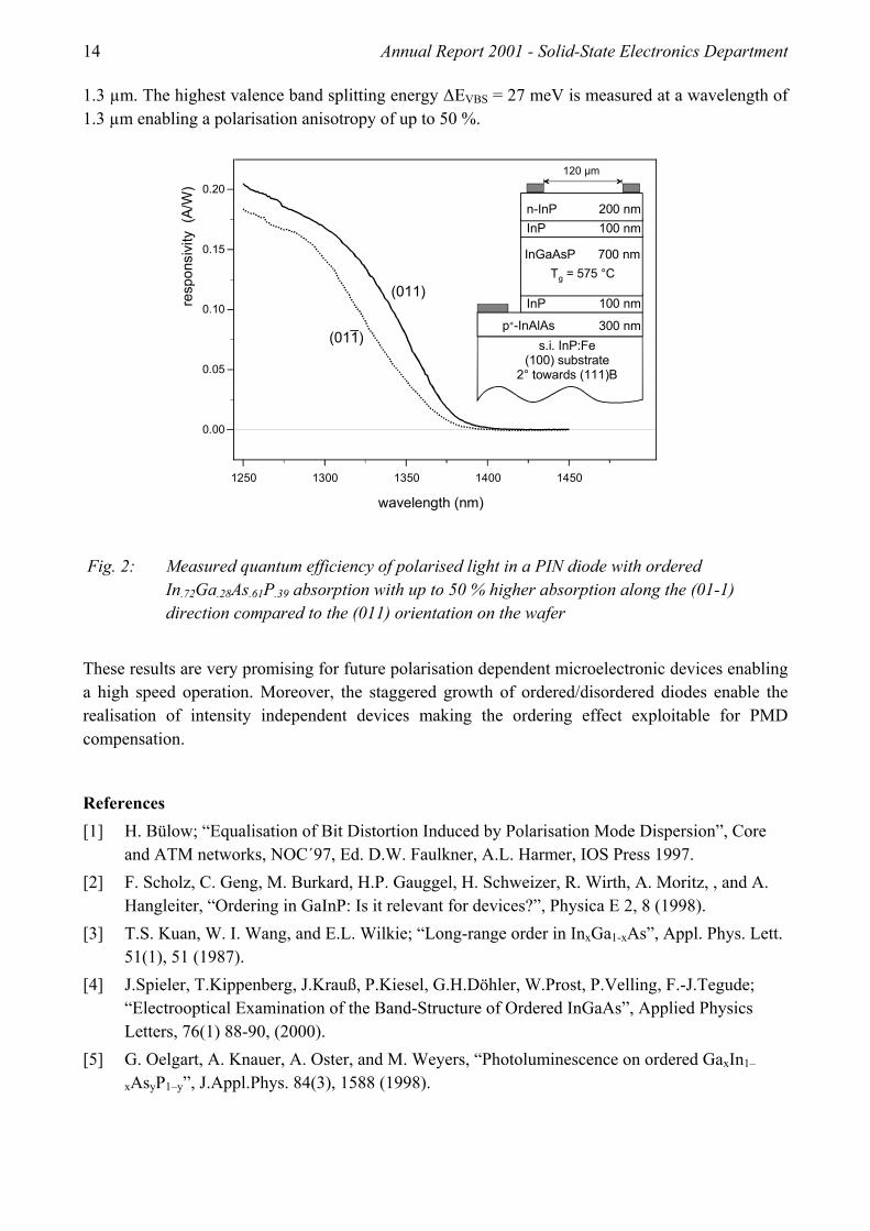
PIN diodes are grown incorporating a thick ordered In1-xGaxAs1-yPy absorption layers sandwiched between transparent p- and n-type contact layers (cf. inset of fig. 2).Devices are fabricated using optical lithography and wet-chemical etching with a window of 120 x 120 µm² (cf. inset of Fig. 2). The I-V characteristic of the device with 700 nm In.72Ga.28As.61P.39 absorption layer grown at 575 °C exhibits a reverse breakdown voltage of 25 V indicating an low background impurity density. The optical anisotropy is investigated for irradiation with polarised light. In Fig. 2 the measured quantum efficiency of polarised light is shown and a strong anisotropy along the (011) and the (01-1) direction of up to 50 % around 1.3 µm is proven.
Discussion
In agreement with previous studies the highest degree of ordering is achieved on (100) substrates tilted by 2° against (111)B [2, 4]. The splitting energy of In1-xGaxAs1-yPy is comparable or even higher than in group-III ordered GaInP/InGaAs indicating a strong additional contribution of group-V ordering. Hence, high quality polarisation dependent devices are available at 1.55 µm and
0
20
25
15
10
5
0 20 40 60 80 100
vale
nce
band
spl
ittin
g en
ergy
EVB
S(m
eV)
P content y in Ga1-xInxAs1-yPy (%)
1550 µm(x=0.58, y = 0.1)
data on InP:Fe (100) 2° (111)B 2° (111)A
fitting
InGaP
data on GaAs (100) 2° (111)B
InGaAs
1300 µm(x=0.72, y = 0.39)
14 Annual Report 2001 - Solid-State Electronics Department
1.3 µm. The highest valence band splitting energy ∆EVBS = 27 meV is measured at a wavelength of 1.3 µm enabling a polarisation anisotropy of up to 50 %.
Fig. 2: Measured quantum efficiency of polarised light in a PIN diode with ordered In.72Ga.28As.61P.39 absorption with up to 50 % higher absorption along the (01-1) direction compared to the (011) orientation on the wafer
These results are very promising for future polarisation dependent microelectronic devices enabling a high speed operation. Moreover, the staggered growth of ordered/disordered diodes enable the realisation of intensity independent devices making the ordering effect exploitable for PMD compensation.
References [1] H. Bülow; “Equalisation of Bit Distortion Induced by Polarisation Mode Dispersion”, Core
and ATM networks, NOC´97, Ed. D.W. Faulkner, A.L. Harmer, IOS Press 1997. [2] F. Scholz, C. Geng, M. Burkard, H.P. Gauggel, H. Schweizer, R. Wirth, A. Moritz, , and A.
Hangleiter, “Ordering in GaInP: Is it relevant for devices?”, Physica E 2, 8 (1998). [3] T.S. Kuan, W. I. Wang, and E.L. Wilkie; “Long-range order in InxGa1-xAs”, Appl. Phys. Lett.
51(1), 51 (1987). [4] J.Spieler, T.Kippenberg, J.Krauß, P.Kiesel, G.H.Döhler, W.Prost, P.Velling, F.-J.Tegude;
“Electrooptical Examination of the Band-Structure of Ordered InGaAs”, Applied Physics Letters, 76(1) 88-90, (2000).
[5] G. Oelgart, A. Knauer, A. Oster, and M. Weyers, “Photoluminescence on ordered GaxIn1–
xAsyP1–y”, J.Appl.Phys. 84(3), 1588 (1998).
1250 1300 1350 1400 1450
0.00
0.05
0.10
0.15
0.20re
spon
sivi
ty (
A/W
)
wavelength (nm)
(011)
(011)
200 nm100 nm
700 nmInGaAsP
InPn-InP
s.i. InP:Fe (100) substrate
2° towards (111)B
300 nm
100 nm
p+-InAlAs
InP
120 µm
Tg = 575 °C
Annual Report 2001 - Solid-State Electronics Department 15
4.1.2 Growth of Carbon doped InAlAs with LP-MOVPE and Non Gaseous Sources
Scientist: S. Neumann Technical Assistant: M. Haase Backround
Highly p-type doped wide bandgap materials are required as window layer for buried, optical transparent, contact layers for 1,55µm and 1,3µm glass fibre applications. The use of carbon for p-type doping has the advantages of the extremely high levels and a negligible diffusion compared to Zn. The possibility of a high doping of InAlAs as wide bandgap material (Eg=1.45 eV) with CBr4 as carbon source in combination with usual group III sources and AsH3 are shown first by Ito et al. [1] (p=7.1018 cm-3) and later by Ougazzaden et al [2] with the highest reported value of p=1.8.1019 cm-3 of electrically activated carbon. In this work, we investigate p-type doping of InAlAs by LP-MOVPE. The use of the alternative precursor TBA exhibit a reduced hazard potential due to their low vapour pressure and their less toxic potential. Another advantage for chosen not gaseous sources is to enable higher doping efficiency and higher layer quality at lower V/III ratio at reduced growth temperature.
Experimental Set-up
The experiments were done on (001)±0.5° orientated s.i. InP:Fe epi-ready substrates in an AIX200-system with rf-heating at 50mbar reactor pressure using N2 carrier gas and a total gas flow of Qtot= 3.4slm. TBAs/TBP/TMAs are used as group V, CBr4 as group IV doping sources and the metal organic sources TMIn, TMAl. After the removal of the oxide from the substrate using TBP for surface stabilization a 50nm thick InP buffer layer is grown at Tg=600°C. A growth temperature range from 600°C down to 520°C was investigated for the growth of the 400nm thick carbon doped InAlAs. A in-situ annealing sequence with TMAs at T>600°C is used to activate the carbon atoms by reducing the passivation. The group-V to group-III ratios (V/III) and also the group-IV to group-III ratios (IV/III) are calculated from the ratio of the partial pressures of the involved precursors by the assumption of 100% source efficiency. The better thermal decomposition of TBA compared to AsH3 enable the growth at low temperature and low V/III ratios. We use a V/III ratio from 5 to achieve a high materiel quality and surface morphology. At lower V/III ratios a degraded surface morphology can be observed. The p-type doping level of the p+-InAlAs:C layers is determined at room temperature by van der Pauw Hall measurements. The quality of the layer structures is proven by HRXRD measurements in the vicinity of the 004 -reflection in a coupled Θ-2Θ-mode using a double monochromator set-up.
16 Annual Report 2001 - Solid-State Electronics Department
Inte
nsity
HRXRD
100
101
103
102
104
300020001000-3000 -2000 -1000 0
M2287Tg=520°Cgr=14nm/minp=4,46.1019cm-3
p-In50Al50As∆a/a=-2160ppm
FWHM (p-InAlAs) =144 arcsec
Seconds
si.-InP-substrate
p-InAlAs 400 nm
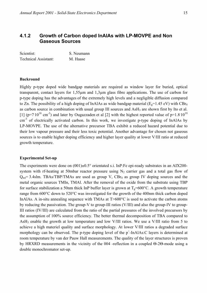
Results and Discussion
In fig. 1 a well defined peak with a high intensity of a strained 400 nm thick C-doped InAlAs layer at p=4.46.1019 cm-3 is obtained.
Fig.: 1 HRXRD measurement of the (004)-reflection of a 400 nm p-InAlAs/InP layer in a coupled Θ-2Θ-mode
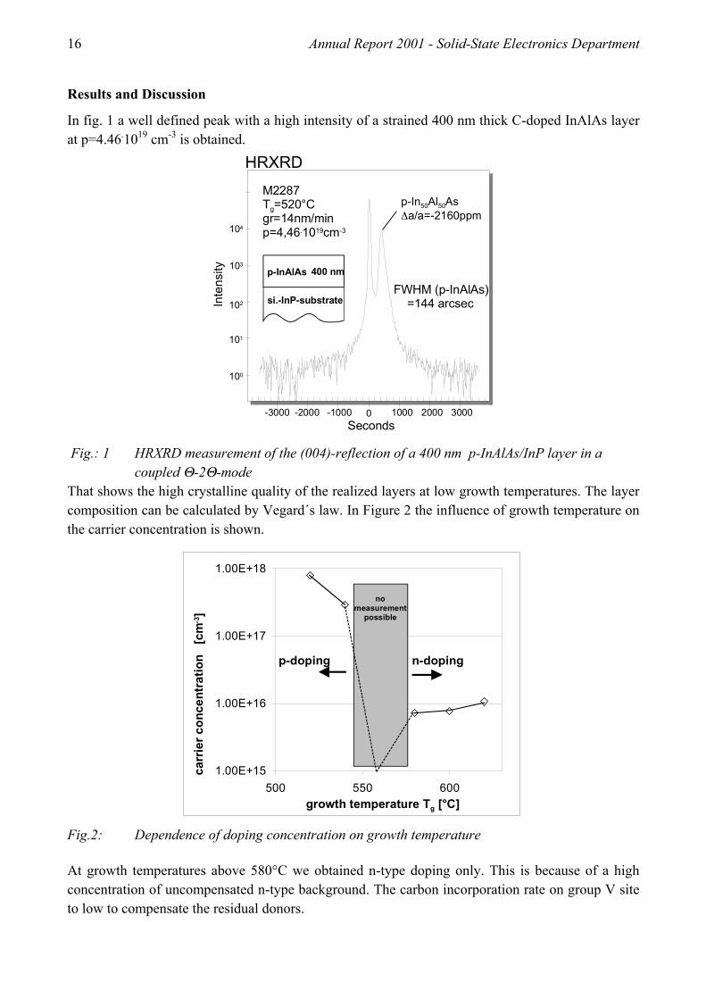
That shows the high crystalline quality of the realized layers at low growth temperatures. The layer composition can be calculated by Vegard´s law. In Figure 2 the influence of growth temperature on the carrier concentration is shown.
Fig.2: Dependence of doping concentration on growth temperature At growth temperatures above 580°C we obtained n-type doping only. This is because of a high concentration of uncompensated n-type background. The carbon incorporation rate on group V site to low to compensate the residual donors.
1.00E+15
1.00E+16
1.00E+17
1.00E+18
500 550 600
carr
ier c
once
ntra
tion
[cm
-3]
growth temperature Tg [°C]
n-dopingp-doping
no measurement
possible
Annual Report 2001 - Solid-State Electronics Department 17
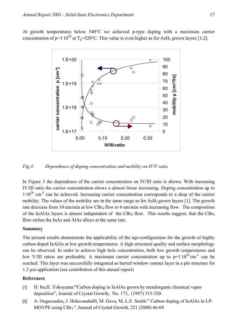
At growth temperatures below 540°C we achieved p-type doping with a maximum carrier concentration of p=1.1020 at Tg=520°C. This value is even higher as for AsH3 grown layers [1,2].
Fig.3: Dependence of doping concentration and mobility on IV/V ratio
In Figure 3 the dependence of the carrier concentration on IV/III ratio is shown. With increasing IV/III ratio the carrier concentration shows a almost linear increasing. Doping concentration up to 1.1020 cm-3 can be achieved. Increasing carrier concentration corresponds to a drop of the carrier mobility. The values of the mobility are in the same range as for AsH3 grown layers [1]. The growth rate decrease from 10 nm/min at low CBr4 flow to 6 nm/min with increasing flow. The composition of the InAlAs layers is almost independent of the CBr4 flow. This results suggest, that the CBr4 flow etches the InAs and AlAs alloys at the same rate.
Summary
The present results demonstrate the applicability of the ngs-configuration for the growth of highly carbon doped InAlAs at low growth temperatures. A high structural quality and surface morphology can be observed. In order to achieve high hole concentration, both low growth temperatures and low V/III ratios are preferable. A maximum carrier concentration up to p=1.1020 cm-3 can be reached. This layer was successfully integrated as buried window contact layer in a pin structure for 1.3 µm application (see contribution of this annual report)
References
[1] H. Ito,H. Yokoyama:”Carbon doping in InAlAs grown by metalorganic chemical vapor deposition”, Journal of Crystal Growth, No. 173, (1997) 315-320
[2] A. Ougazzaden, J. Holavanahalli, M. Geva, M, L.E. Smith:” Carbon doping of InAlAs in LP-MOVPE using CBr4 “, Journal of Crystal Growth, 221 (2000) 66-69
1.E+17
1.E+18
1.E+19
1.E+20
0.00 0.10 0.20 0.300102030405060708090100
carr
ier c
once
ntra
tion
p [c
m-3]
IV/III-ratio
mob
ility
µ [c
m2 /V
s]
18 Annual Report 2001 - Solid-State Electronics Department
0
100
200
300
400
500
600
700
800
X R D F W H M o f In P o n S i su b s tra te :
min 725
min 353
min 155min 90
max 144
(G. P. Tang et al, 1994)
(A. Bartels et al, 1995) (A. Bakin et al, present work)FW
HM
/ ar
csec
4 µm InP 1,5µm InP 2µm GaAs+2µm InP 2µm InP 1,5µm InP
4.1.3 Growth of III/V Resonant Tunnelling Diode on Si Substrate with LP-MOVPE
Scientist: S. Neumann, A. Bakin1)
Technical Assistant: A. Osinski 1): Institut für Halbleitertechnik, A. Schlachetzki, TU Braunschweig
Background
The growth of III-V compound semiconductors on Si substrates was initiated for the monolithically integration of III-V optoelectronics. A variety of heteroepitaxially grown InP based devices, such as laser diodes [1], high- speed phototransistors [2] for optical control have been fabricated on Si-subtrates. Large mismatch of lattice constants (8 % in case of InP on Si), different thermal expansion coefficients and crystal symmetry inevitably cause one- and two-dimensional lattice defects in III/V layers epitaxially grown on Si. But high quality III-V layer growth on Si would allow for combination of resonant tunnelling diodes (RTDs) and CMOS circuits enabling an improvement in circuit functionality, speed and power dissipation. Integration with hybrid technology, flip-chip mounting or epitaxial lift-off of III/V (opto-) electronic components today still remain complicated. First realized III/V RTDs on Si were bonded on a existing CMOS circuit [3] and a first resonant tunnelling CMOS circuit, a clocked 1-bit comparator [4], were demonstrated.
Experimental Setup
The experiments were done on exact (001) orientated Si-substrates in two different LP-MOVPE systems (AIX200) in a cooperative approach of University Braunschweig and Gerhard-Mercator-Universität Duisburg. Standard group-V precursors AsH3/PH3 are used in the LP-MOVPE at University Braunschweig. Alternative group-V precursors TBAs/TBP and a liquid Si group-IV source are used at University Duisburg.
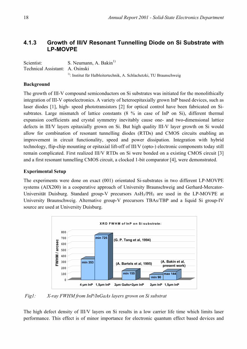
Fig1: X-ray FWHM from InP/InGaAs layers grown on Si substrat
The high defect density of III/V layers on Si results in a low carrier life time which limits laser performance. This effect is of minor importance for electronic quantum effect based devices and
Annual Report 2001 - Solid-State Electronics Department 19
may also have a positive impact on photodetector applications with respect to speed. There are several well-known procedures in order to minimise the defect densities [5].However, up to now most of these procedures suffer from their incompatibility to silicon technology or are not adequate due to complicated and expensive techniques. At TU Braunschweig an InP-growth process is developed which is compatible to Si MOS-technology. By adding a GaAs intermediate layer the width of X-ray rocking curves could be reduced by 50 %. Recently, another 50 % reduction could be achieved, even without GaAs, by patterning the silicon surface on the nanoscale (RMS of about 0.4 nm), thus reducing the technological effort tremendously for growing high quality InP on Si . In Figure 1 the FWHM of the x-ray measurements show the high quality of the realized prepatterned InP layers compared to prior works.
On this prepatterned InP starting layer a RTD is grown on a additional buffer layer. The quality of the layer structures is proven by HRXRD measurements in the vicinity of the 004-reflection in a couped Θ-2Θ-mode using a double monochromator setup. The recorded reflection curves are compared to simulations using BEDE RADS Mercury Optimiser software. Device fabrication is done by wet chemical etching and optical lithography
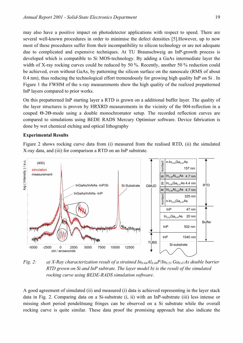
Experimental Results
Figure 2 shows rocking curve data from (i) measured from the realised RTD, (ii) the simulated X-ray data, and (iii) for comparison a RTD on an InP substrate.
Fig. 2: a) X-Ray characterization result of a strained In0.64Al0.46P/In0.53 Ga0.47As double barrier RTD grown on Si and InP subtrate. The layer model b) is the result of the simulated rocking curve using BEDE-RADS simulation software.
A good agreement of simulated (ii) and measured (i) data is achieved representing in the layer stack data in Fig. 2. Comparing data on a Si-substrate (i, ii) with an InP-substrate (iii) less intense or missing short period pendelösung fringes can be observed on a Si substrate while the overall rocking curve is quite similar. These data proof the promising approach but also indicate the
∆Θ / arcseconds
log
( Int
ensi
ty )
/ a.u
.
-5000 -2500 0 2500 75005000 10000 12500
(400)
simulationmeasurement
InGaAs/InAlAs -InP
In0.59Ga0.31As
n-In0.53Ga0.47As
kont
act
Bko
ntac
t
157 nm
4.7 nm
325 nm
In0.38Al0.62As
4.4 nm
4.7 nmIn0.38Al0.62As
BW
n-In0.53Ga0.47As
InP 47 nm
In0.53Ga0.47As 20 nm
InP 502 nm
RTD
Buffer
InP 1540 nm
Si-substrate
GMUD
TUBS
InGaAs/InAlAs -InP/Si Si-Substrate
20 Annual Report 2001 - Solid-State Electronics Department
necessity of further work. With conventional wet chemical etching the first III/V RTD was directly fabricated on Si substrate.
-1-2
0
5
2.5
7.5
-5
-2.5
-7.50 1 2
Vdiode / V
S p /
104 A
/cm
2
AE=2.10 µm2 (nsa)T=300PVR=1.13
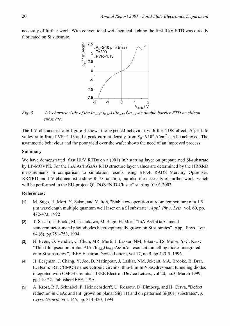
Fig. 3: I-V characteristic of the In0.38Al0.62As/In0.59 Ga0. 41As double barrier RTD on silicon
substrate. The I-V characteristic in figure 3 shows the expected behaviour with the NDR effect. A peak to valley ratio from PVR=1.13 and a peak current density from Sp=6.104 A/cm2 can be achieved. The asymmetric behaviour and the poor yield over the wafer shows the need of an improved process.
Summary
We have demonstrated first III/V RTDs on a (001) InP starting layer on prepatterned Si-substrate by LP-MOVPE. For the InAlAs/InGaAs RTD structure layer values are determined by the HRXRD measurements in comparison to simulation results using BEDE RADS Mercury Optimiser. XRXRD and I-V characteristic show RTD function, but also the necessity of further work which will be performed in the EU-project QUDOS “NID-Cluster” starting 01.01.2002.
References:
[1] M. Sugo, H. Mori, Y. Sakai, and Y. Itoh, "Stable cw operation at room temperature of a 1.5 µm wavelength multiple quantum well laser on a Si substrate", Appl. Phys. Lett., vol. 60, pp. 472-473, 1992
[2] T. Sasaki, T. Enoki, M, Tachikawa, M. Sugo, H. Mori: ”InAlAs/InGaAs metal-semocontuctor-metal photodiodes heteroepitaxially grown on Si subtrates”, Appl. Phys. Lett. 64 (6), pp.751-753, 1994.
[3] N. Evers, O. Vendier, C. Chun, MR. Murti, J. Laskar, NM. Jokerst, TS. Moise, Y-C. Kao : ”Thin film pseudomorphic AlAs/In0.53Ga0.47As/InAs resonant tunnelling diodes integrated onto Si substrates.”, IEEE Electron Device Letters, vol.17, no.9, pp.443-5, 1996.
[4] JI. Bergman, J. Chang, Y. Joo, B. Matinpour, J. Laskar, NM. Jokerst, MA. Brooke, B. Brar, E. Beam:”RTD/CMOS nanoelectronic circuits: thin-film InP-basedresonant tunneling diodes integrated with CMOS circuits.”, IEEE Electron Device Letters, vol.20, no.3, March 1999, pp.119-22. Publisher:IEEE, USA.
[5] A. Krost, R.F. Schnabel, F. Heinrichsdorff, U. Rossow, D. Bimberg, and H. Cerva, "Defect reduction in GaAs and InP grown on planar Si(111) and on patterned Si(001) substrates", J. Cryst. Growth, vol. 145, pp. 314-320, 1994
Annual Report 2001 - Solid-State Electronics Department 21
4.1.4 Investigation of Different Composite-Collector Designs in In0.53Ga0.47As/InP DHBTs
Scientists: T. Reimann, S. Neumann P. Velling (Innovative Processing AG, Duisburg) Technical Assistant: A. Osinski, M. Haase Introduction
Double heterojunction bipolar transistors (DHBTs) make use of wide-band gap material also for the collector. This increases breakdown voltage BVCEO and makes the device useable for circuits in which loads have to be driven with 10 V or higher. But the wide-gap collector has also a disadvantage in the InGaAs/InP material system because of the conduction band offset which is about ∆WC = 275 meV (∆WV = 325 meV) [1]. The band offset reduces electron current from the base to the collector (current blocking effect) and a higher voltage VCE is needed to help electrons tunneling through the barrier. In common-emitter characteristics the effect leads to degraded turn-on behaviour and the available active voltage region is reduced limiting the bias range. The composite collector design, however, is a way to suppress current blocking. Various thin layers were added between the base/collector junction for smoothing the conduction band discontinuity.
Approach and results
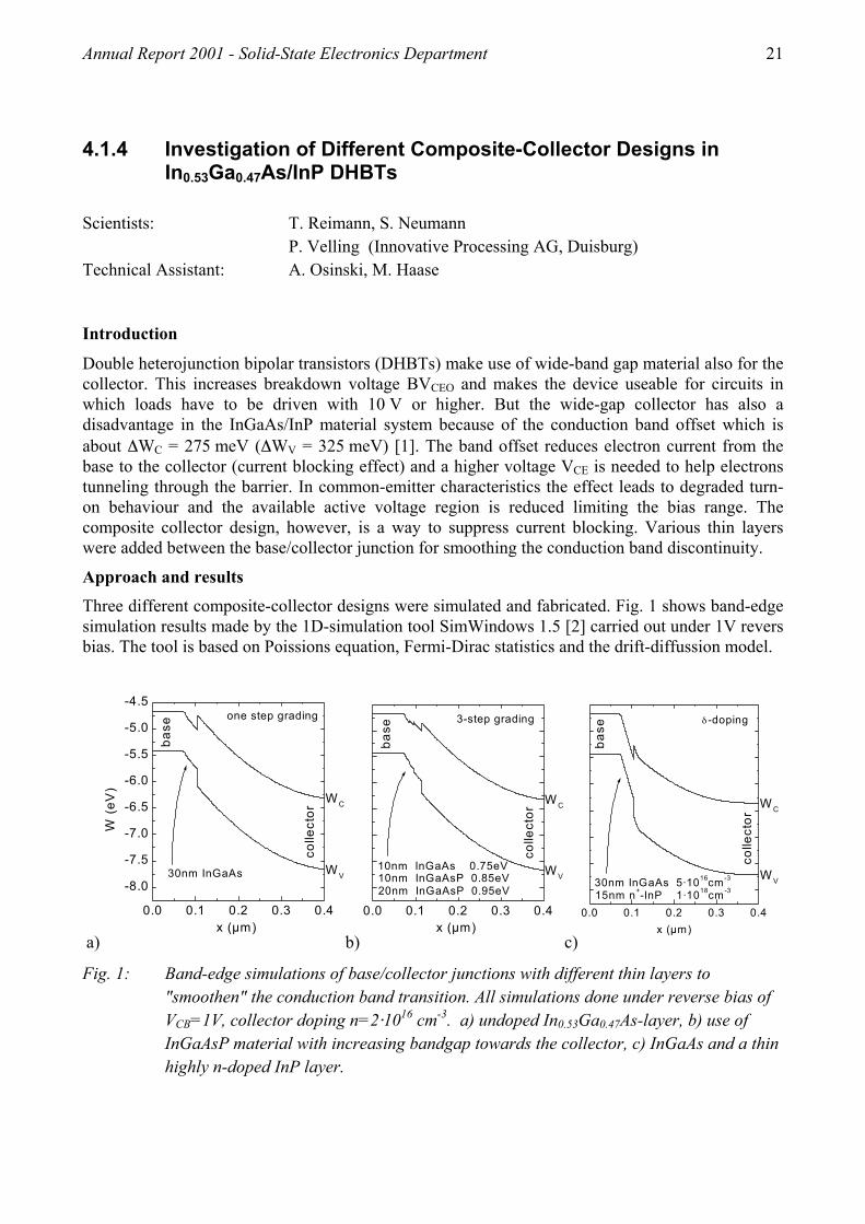
Three different composite-collector designs were simulated and fabricated. Fig. 1 shows band-edge simulation results made by the 1D-simulation tool SimWindows 1.5 [2] carried out under 1V revers bias. The tool is based on Poissions equation, Fermi-Dirac statistics and the drift-diffussion model.
a)
0.0 0.1 0.2 0.3 0.4
-8.0
-7.5
-7.0
-6.5
-6.0
-5.5
-5.0
-4.5
WV
WC
colle
ctor
base
one step grading
30nm InGaAs
W (e
V)
x (µm)b)
0.0 0.1 0.2 0.3 0.4
3-step grading
20nm InGaAsP 0.95eV10nm InGaAsP 0.85eV10nm InGaAs 0.75eV W V
W C
colle
ctor
base
x (µm)c)
0.0 0.1 0.2 0.3 0.4
base
colle
ctor
W V
W C
δ -doping
30nm InGaAs 5·1016cm-3
15nm n+-InP 1·1018cm-3
x (µm)
Fig. 1: Band-edge simulations of base/collector junctions with different thin layers to "smoothen" the conduction band transition. All simulations done under reverse bias of VCB=1V, collector doping n=2⋅1016 cm-3. a) undoped In0.53Ga0.47As-layer, b) use of InGaAsP material with increasing bandgap towards the collector, c) InGaAs and a thin highly n-doped InP layer.
22 Annual Report 2001 - Solid-State Electronics Department
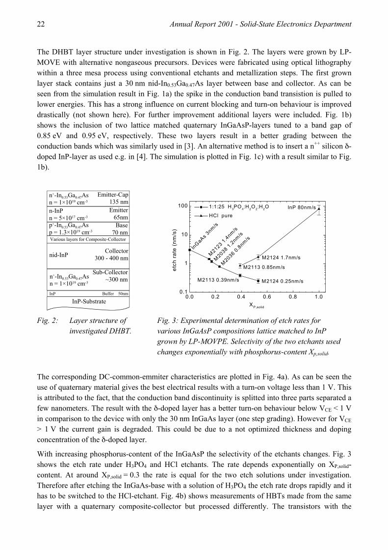
The DHBT layer structure under investigation is shown in Fig. 2. The layers were grown by LP-MOVE with alternative nongaseous precursors. Devices were fabricated using optical lithography within a three mesa process using conventional etchants and metallization steps. The first grown layer stack contains just a 30 nm nid-In0.53Ga0.47As layer between base and collector. As can be seen from the simulation result in Fig. 1a) the spike in the conduction band transistion is pulled to lower energies. This has a strong influence on current blocking and turn-on behaviour is improved drastically (not shown here). For further improvement additional layers were included. Fig. 1b) shows the inclusion of two lattice matched quaternary InGaAsP-layers tuned to a band gap of 0.85 eV and 0.95 eV, respectively. These two layers result in a better grading between the conduction bands which was similarly used in [3]. An alternative method is to insert a n++ silicon δ-doped InP-layer as used e.g. in [4]. The simulation is plotted in Fig. 1c) with a result similar to Fig. 1b).
n+-In0.53Ga0.47Asn = 1×1019 cm-3
n-InPn = 5×1017 cm-3
p+-In0.53Ga0.47Asp = 1.3×1019 cm-3
Emitter-Cap135 nmEmitter
65nmBase
70 nmVarious layers for Composite-Collector
nid-InP
InP-Substrate
Sub-Collector~300 nm
Collector300 - 400 nm
InP Buffer 50nm
n+-In0.53Ga0.47Asn = 1×1019 cm-3
0.0 0.2 0.4 0.6 0.8 1.0
0.1
1
10
100 InP 80nm/s
M2124 1.7nm/s
M2113 0.85nm/s
M2124 0.25nm/sM2113 0.39nm/s
M2036 0.8nm/s
M2038 1.2nm/s
M2123 1.4nm/s
InGaAs 3nm/s
1:1:25 H3PO4:H2O2:H2O
HCl pure
etch
rate
(nm
/s)
XP,solid Fig. 2: Layer structure of Fig. 3: Experimental determination of etch rates for investigated DHBT. various InGaAsP compositions lattice matched to InP grown by LP-MOVPE. Selectivity of the two etchants used changes exponentially with phosphorus-content Xp,solid.
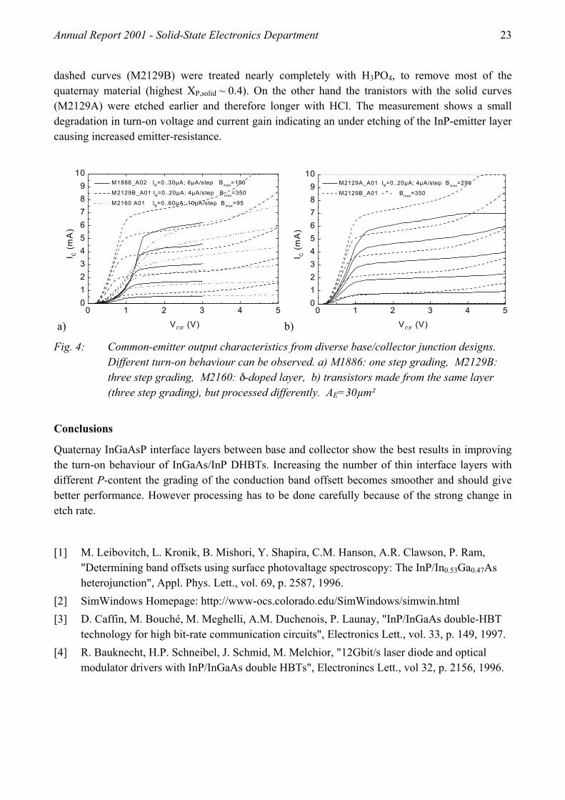
The corresponding DC-common-emmiter characteristics are plotted in Fig. 4a). As can be seen the use of quaternary material gives the best electrical results with a turn-on voltage less than 1 V. This is attributed to the fact, that the conduction band discontinuity is splitted into three parts separated a few nanometers. The result with the δ-doped layer has a better turn-on behaviour below VCE < 1 V in comparison to the device with only the 30 nm InGaAs layer (one step grading). However for VCE > 1 V the current gain is degraded. This could be due to a not optimized thickness and doping concentration of the δ-doped layer.
With increasing phosphorus-content of the InGaAsP the selectivity of the etchants changes. Fig. 3 shows the etch rate under H3PO4 and HCl etchants. The rate depends exponentially on XP,solid-content. At around XP,solid = 0.3 the rate is equal for the two etch solutions under investigation. Therefore after etching the InGaAs-base with a solution of H3PO4 the etch rate drops rapidly and it has to be switched to the HCl-etchant. Fig. 4b) shows measurements of HBTs made from the same layer with a quaternary composite-collector but processed differently. The transistors with the
Annual Report 2001 - Solid-State Electronics Department 23
dashed curves (M2129B) were treated nearly completely with H3PO4, to remove most of the quaternay material (highest XP,solid ~ 0.4). On the other hand the tranistors with the solid curves (M2129A) were etched earlier and therefore longer with HCl. The measurement shows a small degradation in turn-on voltage and current gain indicating an under etching of the InP-emitter layer causing increased emitter-resistance.
a)0 1 2 3 4 5
0123456789
10 M1886_A02 IB=0..30µA; 6µA/step Bmax=180
M2129B_A01 IB=0..20µA; 4µA/step Bmax=350
M2160 A01 IB=0..60µA; 10µA/step Bmax=95
I C (
mA
)
VCE (V) b)0 1 2 3 4 5
0123456789
10 M2129A_A01 IB=0..20µA; 4µA/step Bmax=290
M2129B_A01 - " - Bmax=350
I C (
mA
)
VCE (V)
Fig. 4: Common-emitter output characteristics from diverse base/collector junction designs. Different turn-on behaviour can be observed. a) M1886: one step grading, M2129B: three step grading, M2160: δ-doped layer, b) transistors made from the same layer (three step grading), but processed differently. AE=30µm²
Conclusions
Quaternay InGaAsP interface layers between base and collector show the best results in improving the turn-on behaviour of InGaAs/InP DHBTs. Increasing the number of thin interface layers with different P-content the grading of the conduction band offsett becomes smoother and should give better performance. However processing has to be done carefully because of the strong change in etch rate.
[1] M. Leibovitch, L. Kronik, B. Mishori, Y. Shapira, C.M. Hanson, A.R. Clawson, P. Ram, "Determining band offsets using surface photovaltage spectroscopy: The InP/In0.53Ga0.47As heterojunction", Appl. Phys. Lett., vol. 69, p. 2587, 1996.
[2] SimWindows Homepage: http://www-ocs.colorado.edu/SimWindows/simwin.html [3] D. Caffin, M. Bouché, M. Meghelli, A.M. Duchenois, P. Launay, "InP/InGaAs double-HBT
technology for high bit-rate communication circuits", Electronics Lett., vol. 33, p. 149, 1997. [4] R. Bauknecht, H.P. Schneibel, J. Schmid, M. Melchior, "12Gbit/s laser diode and optical
modulator drivers with InP/InGaAs double HBTs", Electronincs Lett., vol 32, p. 2156, 1996.
24 Annual Report 2001 - Solid-State Electronics Department
4.1.5 Growth and Thermal Desorption of the Thin As Layer for Temporary Passivation of a Semiconductor Surface
Scientists: V. Khorenko, W. Prost Technician: R. Geitmann Present work was carried out within the framework of preparation for the new research project “Nanoparticles in epitaxial heterostructures” within the Sonderforschungsbereich 445 (SFB 445), that will start in January 2002. In this project two, earlier assumed incompatible fabrication techniques should be combined allowing to embed the nanometer-size (5…20 nm) indium particles synthesized in the gas-phase [1] into the epitaxial grown (Al)GaAs layer. It is expected, that these heterostructures will be comparable on their electronic and optical properties with the well-known Stranski-Krastanov quantum dots [2] and at the same time will give much better material, particle sizes and density control [3].
According to the proposed fabrication procedure the substrate should be ex-situ transferred from the molecular beam epitaxy (MBE) chamber to the particle deposition chamber and then back to the MBE. In order to keep during this transfer the substrate surface maximally clean a thin As protect layer should be used. In addition, the initial regrowth temperature after particle deposition should be as low as possible in order to preserve the spherical size of the particles. Our goal in this work was to optimise the growth and thermal desorption parameters of the As layer and to investigate its structure properties and possible degradation upon exposition on the air.
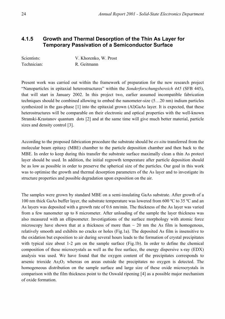
The samples were grown by standard MBE on a semi-insulating GaAs substrate. After growth of a 100 nm thick GaAs buffer layer, the substrate temperature was lowered from 600 ºC to 35 ºC and an As layers was deposited with a growth rate of 0.6 nm/min. The thickness of the As layer was varied from a few nanometer up to 8 micrometer. After unloading of the sample the layer thickness was also measured with an ellipsometer. Investigations of the surface morphology with atomic force microscopy have shown that at a thickness of more than ~ 20 nm the As film is homogenous, relatively smooth and exhibits no cracks or holes (Fig.1a). The deposited As film is insensitive to the oxidation but exposition to air during several hours leads to the formation of crystal precipitates with typical size about 1-2 µm on the sample surface (Fig.1b). In order to define the chemical composition of these microcrystals as well as the free surface, the energy dispersive x-ray (EDX) analysis was used. We have found that the oxygen content of the precipitates corresponds to arsenic trioxide As2O3 whereas on areas outside the precipitates no oxygen is detected. The homogeneous distribution on the sample surface and large size of these oxide microcrystals in comparison with the film thickness point to the Oswald ripening [4] as a possible major mechanism of oxide formation.
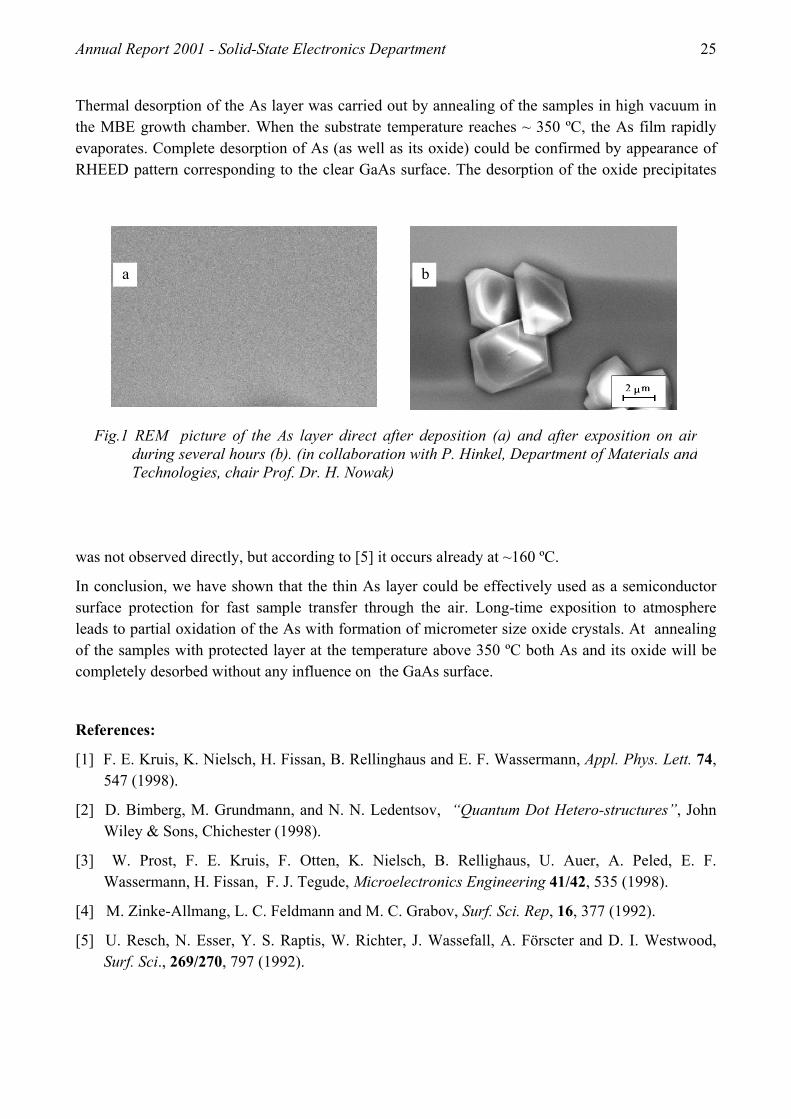
Annual Report 2001 - Solid-State Electronics Department 25
Thermal desorption of the As layer was carried out by annealing of the samples in high vacuum in the MBE growth chamber. When the substrate temperature reaches ~ 350 ºC, the As film rapidly evaporates. Complete desorption of As (as well as its oxide) could be confirmed by appearance of RHEED pattern corresponding to the clear GaAs surface. The desorption of the oxide precipitates
was not observed directly, but according to [5] it occurs already at ~160 ºC.
In conclusion, we have shown that the thin As layer could be effectively used as a semiconductor surface protection for fast sample transfer through the air. Long-time exposition to atmosphere leads to partial oxidation of the As with formation of micrometer size oxide crystals. At annealing of the samples with protected layer at the temperature above 350 ºC both As and its oxide will be completely desorbed without any influence on the GaAs surface.
References:
[1] F. E. Kruis, K. Nielsch, H. Fissan, B. Rellinghaus and E. F. Wassermann, Appl. Phys. Lett. 74, 547 (1998).
[2] D. Bimberg, M. Grundmann, and N. N. Ledentsov, “Quantum Dot Hetero-structures”, John Wiley & Sons, Chichester (1998).
[3] W. Prost, F. E. Kruis, F. Otten, K. Nielsch, B. Rellighaus, U. Auer, A. Peled, E. F. Wassermann, H. Fissan, F. J. Tegude, Microelectronics Engineering 41/42, 535 (1998).
[4] M. Zinke-Allmang, L. C. Feldmann and M. C. Grabov, Surf. Sci. Rep, 16, 377 (1992).
[5] U. Resch, N. Esser, Y. S. Raptis, W. Richter, J. Wassefall, A. Förscter and D. I. Westwood, Surf. Sci., 269/270, 797 (1992).
Fig.1 REM picture of the As layer direct after deposition (a) and after exposition on air
during several hours (b). (in collaboration with P. Hinkel, Department of Materials and Technologies, chair Prof. Dr. H. Nowak)
a b

26 Annual Report 2001 - Solid-State Electronics Department

Annual Report 2001 - Solid-State Electronics Department 27
4.2 Device and Circuit Simulation, Measurement and Modeling
28 Annual Report 2001 - Solid-State Electronics Department
4.2.1 A Consistent PSPICE Model for InP based HBT
Scientist: S. Ehrich Introduction
For simulations of digital circuits based on HBT a model is required which is able to represent the real transistor behaviour. We developed a new analytical large-signal model for InP HBT based on a conventional PSPICE model using subcircuits which allows the description of the real transistor behaviour e.g. including temperature effects and the influence of impact ionization. The specific advantage of the procedure is the numerical stability which allows the simulation of HBT characteristics and HBT circuits as well without any convergence problems.
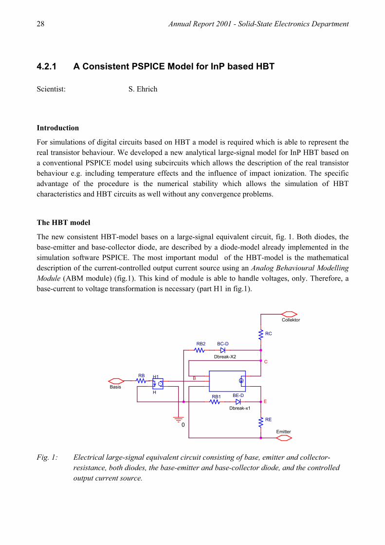
The HBT model
The new consistent HBT-model bases on a large-signal equivalent circuit, fig. 1. Both diodes, the base-emitter and base-collector diode, are described by a diode-model already implemented in the simulation software PSPICE. The most important modul of the HBT-model is the mathematical description of the current-controlled output current source using an Analog Behavioural Modelling Module (ABM module) (fig.1). This kind of module is able to handle voltages, only. Therefore, a base-current to voltage transformation is necessary (part H1 in fig.1).
RB1
RB2
Dbreak-x1
BE-D
0
RC
Dbreak-X2
BC-D
Collektor
C
Basis
RE
Emitter
+-
H1
H
B
E
RB
Fig. 1: Electrical large-signal equivalent circuit consisting of base, emitter and collector-
resistance, both diodes, the base-emitter and base-collector diode, and the controlled output current source.
Annual Report 2001 - Solid-State Electronics Department 29
The complete analytical description of this specific module is given in eq. 1, taking into account all relevant intrinsic and parasitic effects as temperature effects, the influence of impact ionisation as well as leakage-current.
The various parameters of this current-source module are not correlated which allows the separate description of various intrinsic and parasitic effects. Due to the pure analytical character of the procedure high numerical stability is achieved.
(1)
The procedure
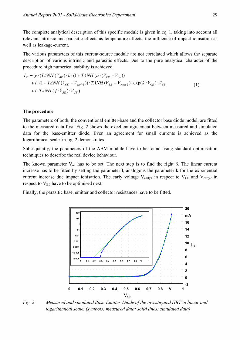
The parameters of both, the conventional emitter-base and the collector base diode model, are fitted to the measured data first. Fig. 2 shows the excellent agreement between measured and simulated data for the base-emitter diode. Even an agreement for small currents is achieved as the logarithmical scale in fig. 2 demonstrates.
Subsequently, the parameters of the ABM module have to be found using standard optimisation techniques to describe the real device behaviour.
The known parameter Von has to be set. The next step is to find the right β. The linear current increase has to be fitted by setting the parameter l, analogous the parameter k for the exponential current increase due impact ionisation. The early voltage Vearly1 in respect to VCE and Vearly2 in respect to VBE have to be optimised next.
Finally, the parasitic base, emitter and collector resistances have to be fitted.
0 0.1 0.2 0.3 0.4 0.5 0.6 0.7 0.8 V 1-2
0
2
4
6
8
10
12
14
16
mA
20
0 0.1 0.2 0.3 0.4 0.5 0.6 0.7 0.8 V 11E-006
1E-005
0.0001
0.001
0.01
0.1
1
mA
100
VCE
IB
Fig. 2: Measured and simulated Base-Emitter-Diode of the investigated HBT in linear and
logarithmical scale. (symbols: measured data; solid lines: simulated data)
))(
)exp()())(1())((1()((
21
CEBE
CBCEearlyBEearlyCE
onCEBEC
VVjTANHi
VVkVVTANHVVTANHlVVaTANHbVTANHyI
⋅⋅⋅+
⋅⋅⋅−⋅−+⋅+
−⋅+⋅⋅⋅=
30 Annual Report 2001 - Solid-State Electronics Department
Comparison between measured and simulated data
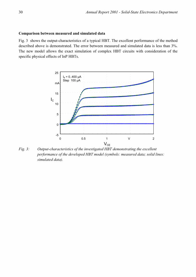
Fig. 3 shows the output-characteristics of a typical HBT. The excellent performance of the method described above is demonstrated. The error between measured and simulated data is less than 3%. The new model allows the exact simulation of complex HBT circuits with consideration of the specific physical effects of InP HBTs.
0 0.5 1 V 2-5
0
5
10
15
mA
25
VCE
IC
IB = 0..400 µAStep 100 µA
Fig. 3: Output-characteristics of the investigated HBT demonstrating the excellent
performance of the developed HBT model (symbols: measured data; solid lines: simulated data).
Annual Report 2001 - Solid-State Electronics Department 31
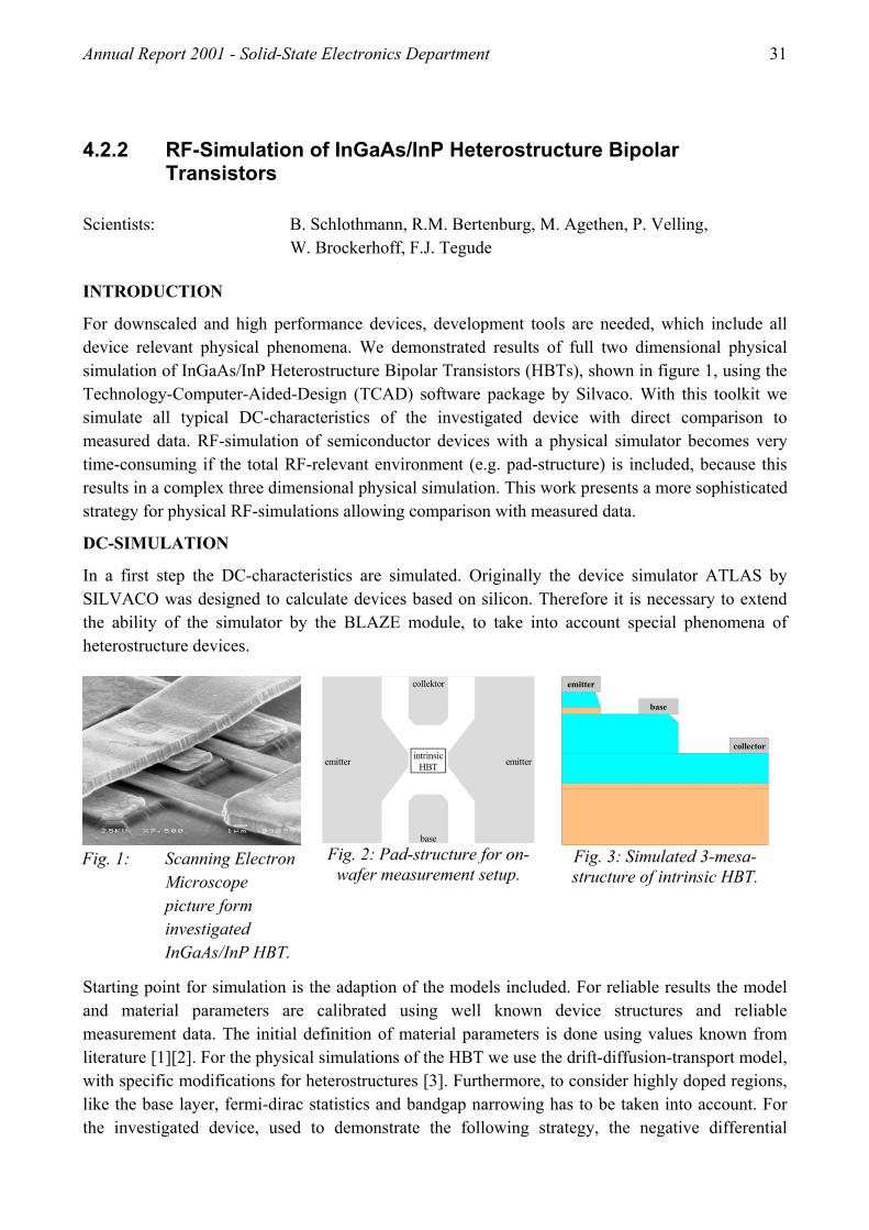
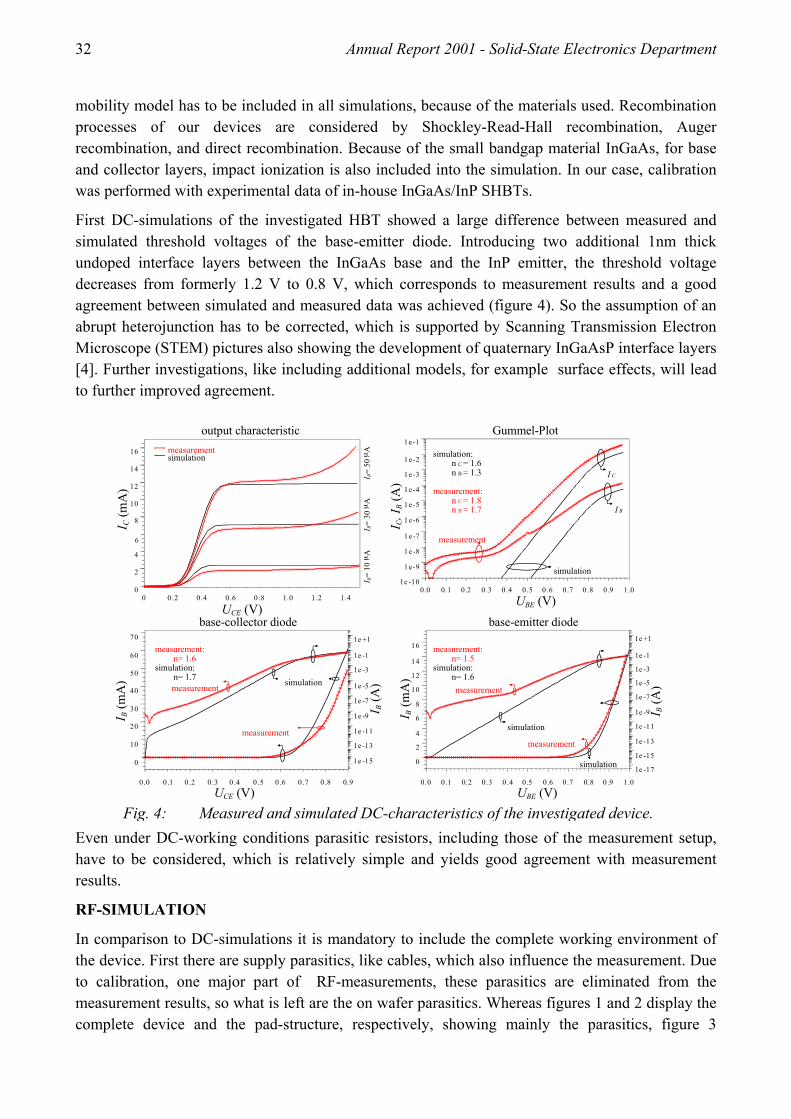
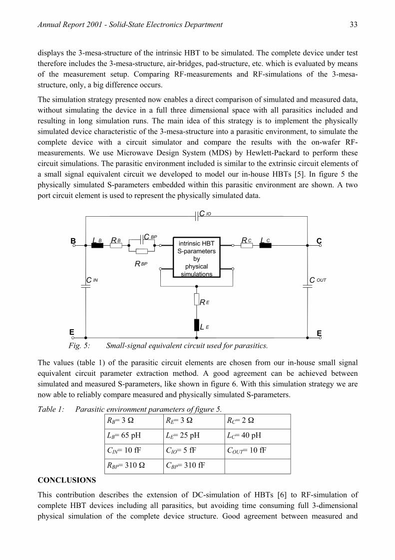
4.2.2 RF-Simulation of InGaAs/InP Heterostructure Bipolar Transistors
Scientists: B. Schlothmann, R.M. Bertenburg, M. Agethen, P. Velling, W. Brockerhoff, F.J. Tegude INTRODUCTION
For downscaled and high performance devices, development tools are needed, which include all device relevant physical phenomena. We demonstrated results of full two dimensional physical simulation of InGaAs/InP Heterostructure Bipolar Transistors (HBTs), shown in figure 1, using the Technology-Computer-Aided-Design (TCAD) software package by Silvaco. With this toolkit we simulate all typical DC-characteristics of the investigated device with direct comparison to measured data. RF-simulation of semiconductor devices with a physical simulator becomes very time-consuming if the total RF-relevant environment (e.g. pad-structure) is included, because this results in a complex three dimensional physical simulation. This work presents a more sophisticated strategy for physical RF-simulations allowing comparison with measured data.
DC-SIMULATION
In a first step the DC-characteristics are simulated. Originally the device simulator ATLAS by SILVACO was designed to calculate devices based on silicon. Therefore it is necessary to extend the ability of the simulator by the BLAZE module, to take into account special phenomena of heterostructure devices.
Starting point for simulation is the adaption of the models included. For reliable results the model and material parameters are calibrated using well known device structures and reliable measurement data. The initial definition of material parameters is done using values known from literature [1][2]. For the physical simulations of the HBT we use the drift-diffusion-transport model, with specific modifications for heterostructures [3]. Furthermore, to consider highly doped regions, like the base layer, fermi-dirac statistics and bandgap narrowing has to be taken into account. For the investigated device, used to demonstrate the following strategy, the negative differential
Fig. 1: Scanning Electron Microscope picture form investigated InGaAs/InP HBT.
base
collektor
emitteremitter intrinsicHBT
Fig. 2: Pad-structure for on-wafer measurement setup.
emitter
base
collector
Fig. 3: Simulated 3-mesa-structure of intrinsic HBT.
32 Annual Report 2001 - Solid-State Electronics Department
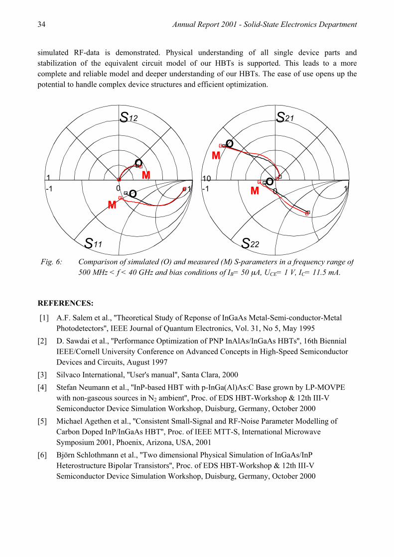
mobility model has to be included in all simulations, because of the materials used. Recombination processes of our devices are considered by Shockley-Read-Hall recombination, Auger recombination, and direct recombination. Because of the small bandgap material InGaAs, for base and collector layers, impact ionization is also included into the simulation. In our case, calibration was performed with experimental data of in-house InGaAs/InP SHBTs.
First DC-simulations of the investigated HBT showed a large difference between measured and simulated threshold voltages of the base-emitter diode. Introducing two additional 1nm thick undoped interface layers between the InGaAs base and the InP emitter, the threshold voltage decreases from formerly 1.2 V to 0.8 V, which corresponds to measurement results and a good agreement between simulated and measured data was achieved (figure 4). So the assumption of an abrupt heterojunction has to be corrected, which is supported by Scanning Transmission Electron Microscope (STEM) pictures also showing the development of quaternary InGaAsP interface layers [4]. Further investigations, like including additional models, for example surface effects, will lead to further improved agreement.
Even under DC-working conditions parasitic resistors, including those of the measurement setup, have to be considered, which is relatively simple and yields good agreement with measurement results.
RF-SIMULATION
In comparison to DC-simulations it is mandatory to include the complete working environment of the device. First there are supply parasitics, like cables, which also influence the measurement. Due to calibration, one major part of RF-measurements, these parasitics are eliminated from the measurement results, so what is left are the on wafer parasitics. Whereas figures 1 and 2 display the complete device and the pad-structure, respectively, showing mainly the parasitics, figure 3
0 0.2 0.4 0.6 0.8 1.21.0 1.40
2
4
6
8
10
12
14
16
output characteristicmeasurementsimulation
0.0 0.1 0.2 0.3 0 .4 0.5 0.6 0.7 0 .8 0.9 1.01e -10
1e-9
1e -8
1e -7
1e -6
1e -5
1e-4
1e-3
1e -2
1e-1Gummel-Plot
simulation:
measurement
simulation
measurement:
0.0 0.1 0.2 0.3 0 .4 0 .5 0.6 0.7 0.8
0
10
20
30
40
50
60
70
1e -15
1e -13
1e -11
1e -9
1e -7
1e -5
1e -3
1e -1
1e +1
0.9
base-collector diode
measurement
measurement simulation
0.0 0.1 0.2 0.3 0.4 0.5 0.6 0.7 0.8 0.9 1 .0
0
2
4
6
8
10
12
14
16
1e -17
1e -15
1e -13
1e -11
1e -9
1e -7
1e -5
1e -3
1e -1
1e +1
base-emitter diode
measurement
measurement
simulation
simulation
n C = 1.6n B = 1.3
n C = 1.8n B = 1.7
measurement:
simulation:n= 1.5
n= 1.6
measurement:
simulation:n= 1.6
n= 1.7
I C
I B
I C (m
A)
I B (m
A)
I B (m
A)
I B (A
)
I B (A
)
UBE (V)
UBE (V)UCE (V)
UCE (V)
I C, I
B (A
)
I B=
10 µ
A
I B=
30 µ
A
I B=
50 µ
A
Fig. 4: Measured and simulated DC-characteristics of the investigated device.
Annual Report 2001 - Solid-State Electronics Department 33
displays the 3-mesa-structure of the intrinsic HBT to be simulated. The complete device under test therefore includes the 3-mesa-structure, air-bridges, pad-structure, etc. which is evaluated by means of the measurement setup. Comparing RF-measurements and RF-simulations of the 3-mesa-structure, only, a big difference occurs.
The simulation strategy presented now enables a direct comparison of simulated and measured data, without simulating the device in a full three dimensional space with all parasitics included and resulting in long simulation runs. The main idea of this strategy is to implement the physically simulated device characteristic of the 3-mesa-structure into a parasitic environment, to simulate the complete device with a circuit simulator and compare the results with the on-wafer RF-measurements. We use Microwave Design System (MDS) by Hewlett-Packard to perform these circuit simulations. The parasitic environment included is similar to the extrinsic circuit elements of a small signal equivalent circuit we developed to model our in-house HBTs [5]. In figure 5 the physically simulated S-parameters embedded within this parasitic environment are shown. A two port circuit element is used to represent the physically simulated data.
The values (table 1) of the parasitic circuit elements are chosen from our in-house small signal equivalent circuit parameter extraction method. A good agreement can be achieved between simulated and measured S-parameters, like shown in figure 6. With this simulation strategy we are now able to reliably compare measured and physically simulated S-parameters.
Table 1: Parasitic environment parameters of figure 5. RB= 3 Ω RE= 3 Ω RC= 2 Ω
LB= 65 pH LE= 25 pH LC= 40 pH
CIN= 10 fF CIO= 5 fF COUT= 10 fF
RBP= 310 Ω CBP= 310 fF
CONCLUSIONS
This contribution describes the extension of DC-simulation of HBTs [6] to RF-simulation of complete HBT devices including all parasitics, but avoiding time consuming full 3-dimensional physical simulation of the complete device structure. Good agreement between measured and
intrinsic HBTS-parameters
byphysical
simulations
C IO
C IN C OUT
C BP
R BP
R BL B R C L C
R E
L EE E
CB
Fig. 5: Small-signal equivalent circuit used for parasitics.
34 Annual Report 2001 - Solid-State Electronics Department
simulated RF-data is demonstrated. Physical understanding of all single device parts and stabilization of the equivalent circuit model of our HBTs is supported. This leads to a more complete and reliable model and deeper understanding of our HBTs. The ease of use opens up the potential to handle complex device structures and efficient optimization.
REFERENCES:
[1] A.F. Salem et al., ''Theoretical Study of Reponse of InGaAs Metal-Semi-conductor-Metal Photodetectors'', IEEE Journal of Quantum Electronics, Vol. 31, No 5, May 1995
[2] D. Sawdai et al., ''Performance Optimization of PNP InAlAs/InGaAs HBTs'', 16th Biennial IEEE/Cornell University Conference on Advanced Concepts in High-Speed Semiconductor Devices and Circuits, August 1997
[3] Silvaco International, ''User's manual'', Santa Clara, 2000 [4] Stefan Neumann et al., ''InP-based HBT with p-InGa(Al)As:C Base grown by LP-MOVPE
with non-gaseous sources in N2 ambient'', Proc. of EDS HBT-Workshop & 12th III-V Semiconductor Device Simulation Workshop, Duisburg, Germany, October 2000
[5] Michael Agethen et al., ''Consistent Small-Signal and RF-Noise Parameter Modelling of Carbon Doped InP/InGaAs HBT'', Proc. of IEEE MTT-S, International Microwave Symposium 2001, Phoenix, Arizona, USA, 2001
[6] Björn Schlothmann et al., ''Two dimensional Physical Simulation of InGaAs/InP Heterostructure Bipolar Transistors'', Proc. of EDS HBT-Workshop & 12th III-V Semiconductor Device Simulation Workshop, Duisburg, Germany, October 2000
S22
S21
S11
S12
OM
OM
OM
OM1
-1 10 0 1-110
Fig. 6: Comparison of simulated (O) and measured (M) S-parameters in a frequency range of
500 MHz < f < 40 GHz and bias conditions of IB= 50 µA, UCE= 1 V, IC= 11.5 mA.
Annual Report 2001 - Solid-State Electronics Department 35
f = 1.0 GHz
-0,06
-0,04
-0,02
0
0,02
0,04
0,06
0 0,2 0,4 0,6 0,8 1
time [ns]
absolute erroroutin
4.2.3 Development of a Calibration Procedure for High-speed Time Domain Measurements
Student: T. Gernandt Scientist: H. van Husen
Introduction
Losses on transmission lines hardly influence the performance of digital circuits at lower frequencies. But, in high-speed time domain measurement phenomena such as rise time degrad-ation, added delays and bandwidth reduction must be considered. Skin effect and dielectric losses are the most important causes of these effects. For exact and correct measurements coaxial cable and probe tips, respectively, to connect the digital circuits has to be carefully characterized using the method described in the paper “Practical Characterization of Lossy Transmission Lines” [1].
Measurement including lossy effects
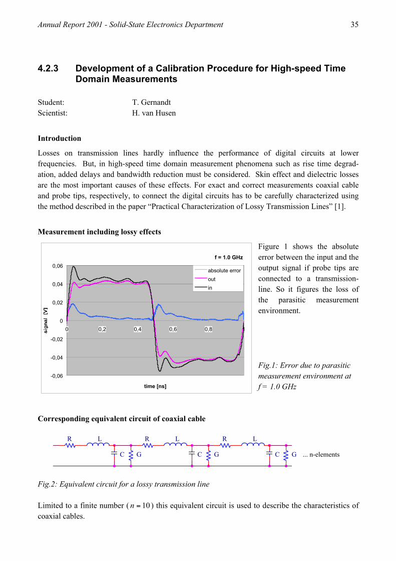
Figure 1 shows the absolute error between the input and the output signal if probe tips are connected to a transmission-line. So it figures the loss of the parasitic measurement environment.
Fig.1: Error due to parasitic measurement environment at f = 1.0 GHz
Corresponding equivalent circuit of coaxial cable
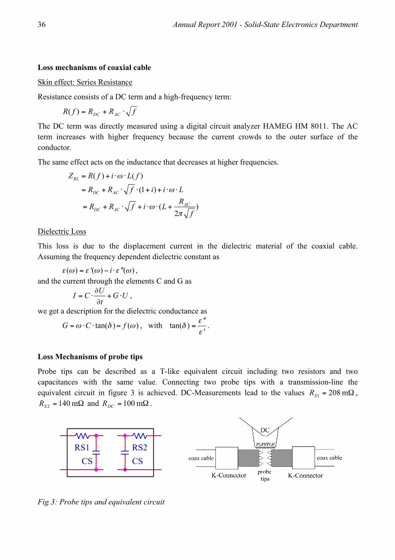
Fig.2: Equivalent circuit for a lossy transmission line Limited to a finite number ( 10=n ) this equivalent circuit is used to describe the characteristics of coaxial cables.
RR L
G ... n-elements
L
C
LR
GC C G
36 Annual Report 2001 - Solid-State Electronics Department
Loss mechanisms of coaxial cable
Skin effect: Series Resistance
Resistance consists of a DC term and a high-frequency term:
fRRfR ACDC ⋅+=)(
The DC term was directly measured using a digital circuit analyzer HAMEG HM 8011. The AC term increases with higher frequency because the current crowds to the outer surface of the conductor.
The same effect acts on the inductance that decreases at higher frequencies.
( ) ( )
(1 )RL
DC AC
Z R f i L f
R R f i i L
ω
ω
= + ⋅ ⋅
= + ⋅ ⋅ + + ⋅ ⋅
Dielectric Loss
This loss is due to the displacement current in the dielectric material of the coaxial cable. Assuming the frequency dependent dielectric constant as
( ) '( ) ''( )iε ω ε ω ε ω= − ⋅ , and the current through the elements C and G as
UI C G Ut
∂= ⋅ + ⋅
∂,
we get a description for the dielectric conductance as
tan( ) ( )G C fω δ ω= ⋅ ⋅ = , with ''tan( )'
εδ
ε= .
Loss Mechanisms of probe tips
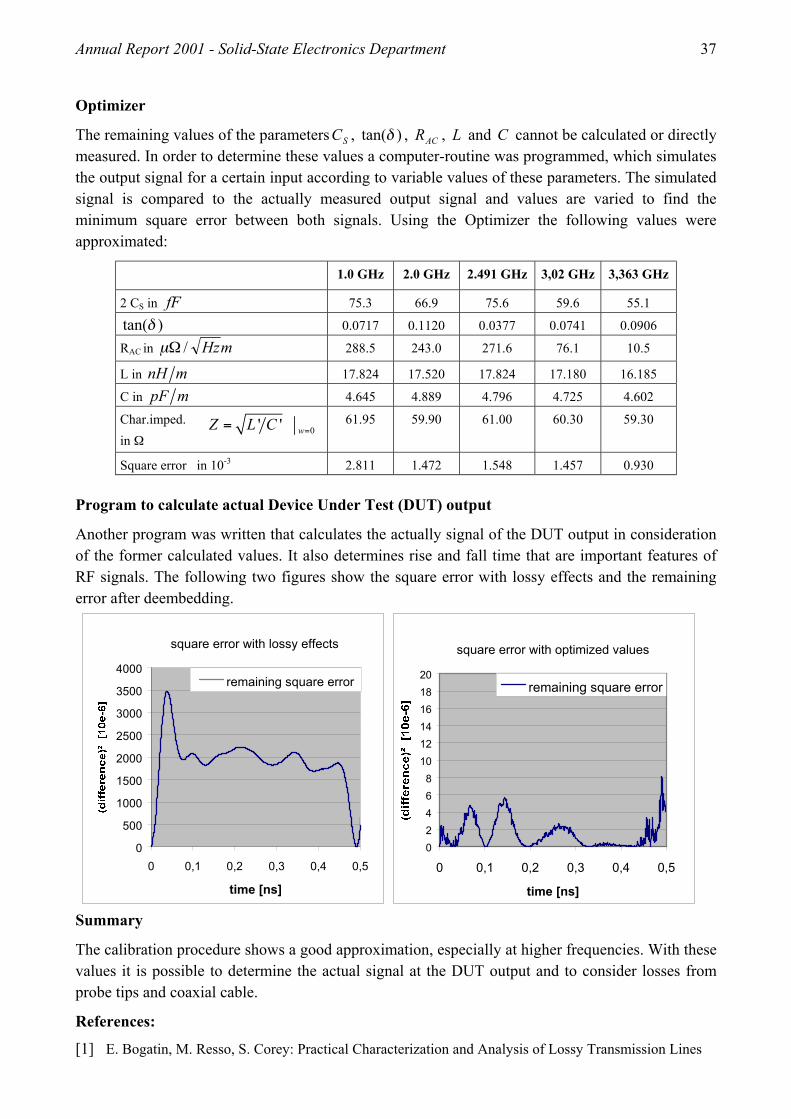
Probe tips can be described as a T-like equivalent circuit including two resistors and two capacitances with the same value. Connecting two probe tips with a transmission-line the equivalent circuit in figure 3 is achieved. DC-Measurements lead to the values Ω= m 2081SR ,
Ω= m 1402SR and Ω= m 100DCR .
Fig.3: Probe tips and equivalent circuit
( )2
ACDC AC
RR R f i Lf
ωπ
= + ⋅ + ⋅ ⋅ +
RS2RS1CSCS
Annual Report 2001 - Solid-State Electronics Department 37
Optimizer
The remaining values of the parameters SC , )tan(δ , ACR , L and C cannot be calculated or directly measured. In order to determine these values a computer-routine was programmed, which simulates the output signal for a certain input according to variable values of these parameters. The simulated signal is compared to the actually measured output signal and values are varied to find the minimum square error between both signals. Using the Optimizer the following values were approximated:
Program to calculate actual Device Under Test (DUT) output
Another program was written that calculates the actually signal of the DUT output in consideration of the former calculated values. It also determines rise and fall time that are important features of RF signals. The following two figures show the square error with lossy effects and the remaining error after deembedding.
Summary
The calibration procedure shows a good approximation, especially at higher frequencies. With these values it is possible to determine the actual signal at the DUT output and to consider losses from probe tips and coaxial cable.
References:
[1] E. Bogatin, M. Resso, S. Corey: Practical Characterization and Analysis of Lossy Transmission Lines
1.0 GHz 2.0 GHz 2.491 GHz 3,02 GHz 3,363 GHz
2 CS in fF 75.3 66.9 75.6 59.6 55.1
)tan(δ 0.0717 0.1120 0.0377 0.0741 0.0906
RAC in mHz/Ωµ 288.5 243.0 271.6 76.1 10.5
L in nH m 17.824 17.520 17.824 17.180 16.185
C in pF m 4.645 4.889 4.796 4.725 4.602
Char.imped. in Ω
61.95 59.90 61.00 60.30 59.30
Square error in 10-3 2.811 1.472 1.548 1.457 0.930
square error with lossy effects
0
500
1000
1500
2000
2500
3000
3500
4000
0 0,1 0,2 0,3 0,4 0,5
time [ns]
remaining square error
square error with optimized values
02468
101214161820
0 0,1 0,2 0,3 0,4 0,5
time [ns]
remaining square error
0' ' wZ L C ==

38 Annual Report 2001 - Solid-State Electronics Department
4.2.4 Design, Build-Up and Testing of a Full Digital Controller for DC/DC-Converters
Student: J. Driesen Supervisor: R.M. Bertenburg Introduction
The work was carried out in cooperation with Infineon Technologies, Angermund, Germany.
Modern applications need a long life power supply with high efficiency. Especially for mobile com-munications and other hand held devices – where usually storage-batteries are used – the highly efficient use of the charge is crucial.
A headset for use in mobile communications implementing the Bluetooth radio standard is used as a background application for the design realised in this work. Normally, linear voltage regulators are implemented in this type of applications. The step-down or buck converter described in this work was designed to improve the efficiency while offering a low output voltage as it is needed for future ICs. A linear regulator would have an efficiency of 28%, while the step-down converter in this design achieves an efficiency of about 85%.
Principles
To perfom the conversion from one DC voltage into a higher or lower one, the converter switches the input voltage. It takes energy portions from the source, filters it through an LC filter and provides a lower DC voltage for the resistive load.
Fig. 1: Schematic of the step-down converter structure. The control provides a pulse width modulated square wave signal at its output to drive transistor T1. The signal is derived by measuring the output voltage UA.
Figure 1 shows the structure of this converter type. Effectively, the inductor reduces the current ripple of the resulting square wave signal behind the switch while the capacitor reduces the voltage ripple.
Two operating modes of the cicuit can be distinguished. In the first mode – the continuous current mode – a current always flows through the inductor, as it is described above. The output voltage of the circuit then can be assumed as
EidealEON
A UpUT
tU ⋅=⋅= ,
with the turn-on time tON, the time of the whole cycle T and the resulting ideal pulse width pideal.
Annual Report 2001 - Solid-State Electronics Department 39
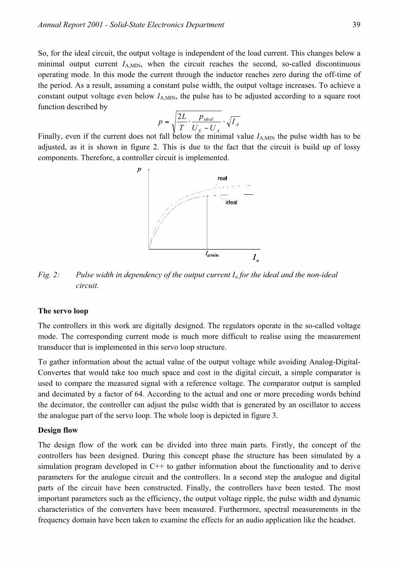
So, for the ideal circuit, the output voltage is independent of the load current. This changes below a minimal output current IA,MIN, when the circuit reaches the second, so-called discontinuous operating mode. In this mode the current through the inductor reaches zero during the off-time of the period. As a result, assuming a constant pulse width, the output voltage increases. To achieve a constant output voltage even below IA,MIN, the pulse has to be adjusted according to a square root function described by
AAE
ideal IUU
pTLp ⋅
−⋅=
2
Finally, even if the current does not fall below the minimal value IA,MIN the pulse width has to be adjusted, as it is shown in figure 2. This is due to the fact that the circuit is build up of lossy components. Therefore, a controller circuit is implemented.
Fig. 2: Pulse width in dependency of the output current Ia for the ideal and the non-ideal circuit.
The servo loop
The controllers in this work are digitally designed. The regulators operate in the so-called voltage mode. The corresponding current mode is much more difficult to realise using the measurement transducer that is implemented in this servo loop structure.
To gather information about the actual value of the output voltage while avoiding Analog-Digital-Convertes that would take too much space and cost in the digital circuit, a simple comparator is used to compare the measured signal with a reference voltage. The comparator output is sampled and decimated by a factor of 64. According to the actual and one or more preceding words behind the decimator, the controller can adjust the pulse width that is generated by an oscillator to access the analogue part of the servo loop. The whole loop is depicted in figure 3.
Design flow
The design flow of the work can be divided into three main parts. Firstly, the concept of the controllers has been designed. During this concept phase the structure has been simulated by a simulation program developed in C++ to gather information about the functionality and to derive parameters for the analogue circuit and the controllers. In a second step the analogue and digital parts of the circuit have been constructed. Finally, the controllers have been tested. The most important parameters such as the efficiency, the output voltage ripple, the pulse width and dynamic characteristics of the converters have been measured. Furthermore, spectral measurements in the frequency domain have been taken to examine the effects for an audio application like the headset.
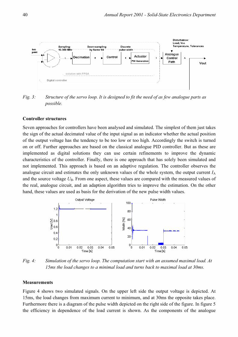
40 Annual Report 2001 - Solid-State Electronics Department
Fig. 3: Structure of the servo loop. It is designed to fit the need of as few analogue parts as possible.
Controller structures
Seven approaches for controllers have been analysed and simulated. The simplest of them just takes the sign of the actual decimated value of the input signal as an indicator whether the actual position of the output voltage has the tendency to be too low or too high. Accordingly the switch is turned on or off. Further approaches are based on the classical analogue PID controller. But as these are implemented as digital solutions they can use certain refinements to improve the dynamic characteristics of the controller. Finally, there is one approach that has solely been simulated and not implemented. This approach is based on an adaptive regulation. The controller observes the analogue circuit and estimates the only unknown values of the whole system, the output current IA and the source voltage UB. From one aspect, these values are compared with the measured values of the real, analogue circuit, and an adaption algorithm tries to improve the estimation. On the other hand, these values are used as basis for the derivation of the new pulse width values.
Fig. 4: Simulation of the servo loop. The computation start with an assumed maximal load. At 15ms the load changes to a minimal load and turns back to maximal load at 30ms.
Measurements
Figure 4 shows two simulated signals. On the upper left side the output voltage is depicted. At 15ms, the load changes from maximum current to minimum, and at 30ms the opposite takes place. Furthermore there is a diagram of the pulse width depicted on the right side of the figure. In figure 5 the efficiency in dependence of the load current is shown. As the components of the analogue
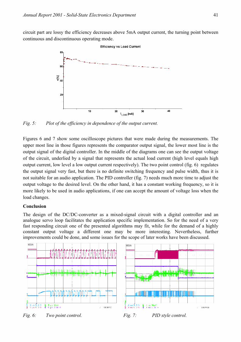
Annual Report 2001 - Solid-State Electronics Department 41
circuit part are lossy the efficiency decreases above 5mA output current, the turning point between continuous and discontinuous operating mode.
Fig. 5: Plot of the efficiency in dependence of the output current.
Figures 6 and 7 show some oscilloscope pictures that were made during the measurements. The upper most line in those figures represents the comparator output signal, the lower most line is the output signal of the digital controller. In the middle of the diagrams one can see the output voltage of the circuit, underlied by a signal that represents the actual load current (high level equals high output current, low level a low output current respectively). The two point control (fig. 6) regulates the output signal very fast, but there is no definite switching frequency and pulse width, thus it is not suitable for an audio application. The PID controller (fig. 7) needs much more time to adjust the output voltage to the desired level. On the other hand, it has a constant working frequency, so it is more likely to be used in audio applications, if one can accept the amount of voltage loss when the load changes.
Conclusion
The design of the DC/DC-converter as a mixed-signal circuit with a digital controller and an analogue servo loop facilitates the application specific implementation. So for the need of a very fast responding circuit one of the presented algorithms may fit, while for the demand of a highly constant output voltage a different one may be more interesting. Nevertheless, further improvements could be done, and some issues for the scope of later works have been discussed.
Fig. 6: Two point control. Fig. 7: PID style control.

42 Annual Report 2001 - Solid-State Electronics Department
4.2.5 Automated Wafer Probing
Student: O. El Alami Scientist: M. Agethen, S. Ehrich Introduction
The DC-characterization and statistical analysis of semiconductor devices provide information aboutquality and fabrication process - information that can be used to improve process efficiency and yield. The measurement of complete wafers on manual wafer probe stations is very time-consuming and can be simplified enormously by the use of full-automatic or semi-automatic wafer probers. Within this work a program controlled probing solution in combination with a measurement system for DC-characterization of heterojunction bipolar transistors (HBT) has been developed. Function and Solution The program, which has been developed using the graphical programming tool Agilent VEE for MS Windows, contains the semi-automatic wafer probe station SUSS PA150 and an HP4145 parameter analyser. It can be used to control automated measurements and wafer prober movements via the GPIB interface (IEEE488). The system developed allows a device-by-device measurement of complete wafers of any lateral device arrangement and enables an additional of other measurement methods for different devices like field effect transistors. Defect devices are identified and catalogued as a reject by the program. This makes possible statistical analysis like yield and variation of output characteristics of a single device type over a complete wafer. Several steps are necessary to realize this flexible program-controlled system: The first step is the preparation of a mask data file, in which the operator collects the layout information of the design. A prepared mask data file can be loaded into the program and allows flexible use of various mask types. The second step is the use of a two-point alignment to correct the rotational placement error by the program. This enables a precise positioning of a device relative to a set of probe tips. After contacting a reference device, the operator defines the optimal parameters for measuring the DC-characteristics. The data of the reference measurements can be used later for analysis of defect devices. After each device measurement the detection of defects begins. Defects in layout or on wafer can cause electrical short, open or other failures. By using the reference data these defects can be identified by the program. If a faulty device is detected the remaining DC-characteristics are skipped to save time. The statistical evaluation of a single device type starts after the examination of the complete wafer.
Annual Report 2001 - Solid-State Electronics Department 43
The results of the measurements and the statistical analysis are stored in ASCII files and may be loaded back into the program or imported into external software like EXCEL or ORIGIN for later visualization. Results To demonstrate the capabilities of the program a test wafer (M2106) was measured and the results of the statistical analysis are visualized (fig.1 and fig. 2). Figure 1 shows the result of a non self-aligned (A01) and a self-aligned (A27) HBT. All cells available on the wafer were selected for measurement. The distribution of one HBT type and the yield is illustrated in a wafer map, which gives a fast und easy feedback to the operator. The device state in a cell on the wafer map is coded in the following way:
• Crossed - cell not available for measurement • Hatched - failed device • Blank - passed device
B6
A6 A7A5
96 979594 98
86 878584 8883
72 76 777574 7873
62 66 676564 686361
52 56 575554 5853
46 474544 4843
36 373534 38
26 2725
16A01
52.5 %
B6
A6 A7A5
96 979594 98
86 878584 8883
72 76 777574 7873
62 66 676564 686361
52 56 575554 5853
46 474544 4843
36 373534 38
26 2725
16A27
40 %
Fig.1: Wafer map and yield of non self-aligned and self-aligned HBT (M2106, AE=30µm2) A typical distribution is shown in the right wafer map. Faulty devices are often localized at the periphary of the wafer due to photo resist inhomogeneity during processing. The left wafer map displays a inhomogeneous distribution due to non-uniform epitaxy or/and process technology. The mean values and the variation of common emitter DC-output characteristics are diagrammed in figure 2. It represents the quality and the reproducibility of the investigated device type. The tested HBT (A01) shows variations with respect to different turn-on voltage and current gain.
44 Annual Report 2001 - Solid-State Electronics Department
0.0 0.2 0.4 0.6 0.8 1.0 1.2
02468
1012141618
I B =
0...
40 µ
A
I C (
mA
)
UCE (V)
Fig. 2: Mean and variation of common emitter DC-outputs Conclusion The program developed allows automated measurements of complete wafers on a semi-automatic wafer probe station. Complete wafer maps of data that took hours to measure manually can now be finished in a shorter time. This will allow much more data to be collected than in the past and will lead to a better characterization of device performance and give feedback for process technology.
Annual Report 2001 - Solid-State Electronics Department 45
4.3 Device and Circuit Processing and Characterization
46 Annual Report 2001 - Solid-State Electronics Department
4.3.1 Lithographic Tools for Laterally Controlled Nanocrystal Deposition
Scientist: F. Otten in collaboration with: F.E. Kruis, H. Fißan
(Dept. of Process- and Aerosol Technology, Prof. H. Fißan) Introduction
Quantum devices have minimum feature sizes of a few nanometers. Producing small structures (d< 50 nm) by high resolution lithography reaches the economical and physical limits. The use of simpler nanopatterning techniques result in loss of structure control and engineering design. The goal of this research project is to implement the gas-phase synthesis of nanostructures [1] into microelectronic technology to fulfill the design control.
Electrostatic lenses formed by charged and patterned 500 nm thick photo resist are employed to control the deposition process of the nanoparticles. This technique is a parallel process and has therefore a big advantage compared to serial pattern definition e.g. by electron beam lithography [2]. In fig.1a) the electric field of the electrostatic lenses and b) a SEM figure of deposited 20 nm PbS nanocrystals are depicted. Nanocrystals are collected from a projected area with a diameter of 3 µm and focussed into the 1 µm wide open area. The superposition of the applied field of 2 kV/cm with this coming from the electrostatic lenses results in a field of 0.6 kV/cm in 2 µm distance above the substrate.
(a) (b)
Fig.1: (a) Result of a Quickfield® simulation of an electrostatic field of patterned photo resist
charged with 500 charges / µm2 on top of s.i. GaAs substrate in a deposition chamber with an external field of 2 kV/cm. Within the box the field lines are decreased by a factor of 5 for visibility. The broken guide lines are to identify the hopper-like focussing of the nanocrystals deposition. (b) SEM picture of s.i. GaAs substrate (1) with patterned photo resist (2) and deposited 20 nm PbS nanocrystals (3).
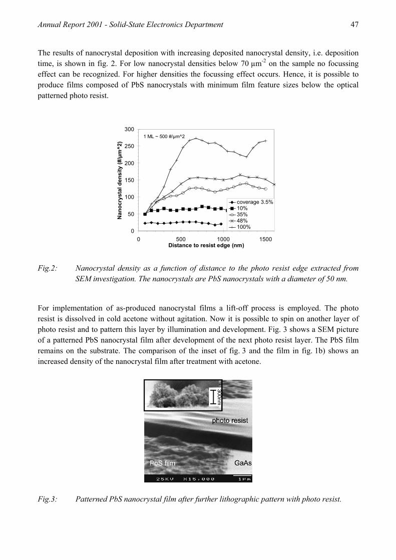
Annual Report 2001 - Solid-State Electronics Department 47
The results of nanocrystal deposition with increasing deposited nanocrystal density, i.e. deposition time, is shown in fig. 2. For low nanocrystal densities below 70 µm-2 on the sample no focussing effect can be recognized. For higher densities the focussing effect occurs. Hence, it is possible to produce films composed of PbS nanocrystals with minimum film feature sizes below the optical patterned photo resist.
0
50
100
150
200
250
300
0 500 1000 1500Distance to resist edge (nm)
Nan
ocry
stal
den
sity
(#/µ
m^2
)
coverage 3.5%10%35%48%100%
1 ML ~ 500 #/µm^2
Fig.2: Nanocrystal density as a function of distance to the photo resist edge extracted from
SEM investigation. The nanocrystals are PbS nanocrystals with a diameter of 50 nm. For implementation of as-produced nanocrystal films a lift-off process is employed. The photo resist is dissolved in cold acetone without agitation. Now it is possible to spin on another layer of photo resist and to pattern this layer by illumination and development. Fig. 3 shows a SEM picture of a patterned PbS nanocrystal film after development of the next photo resist layer. The PbS film remains on the substrate. The comparison of the inset of fig. 3 and the film in fig. 1b) shows an increased density of the nanocrystal film after treatment with acetone.
Fig.3: Patterned PbS nanocrystal film after further lithographic pattern with photo resist.
48 Annual Report 2001 - Solid-State Electronics Department
Acknowledgement
The authors would like to thank T. Krinke for fruitful discussions on the gas-phase deposition mechanisms and W. Kunze from Low-Temperature Physics Dept. for his support with the SEM. The financial support by Deutsche Forschungsgemeinschaft is greatly acknowledged.
References:
[1] F.E. Kruis, K. Nielsch, H. Fissan, B. Rellinghaus and E.F. Wassermann: Appl. Phys. Lett., 1998, 74, 547.
[2] W. Prost, F.E. Kruis, F. Otten, K. Nielsch, B. Rellinghaus, U. Auer, A. Peled, E.F. Wassermann, H. Fissan and F.J. Tegude, Microelectron. Eng.,1998, 41/42, 535.
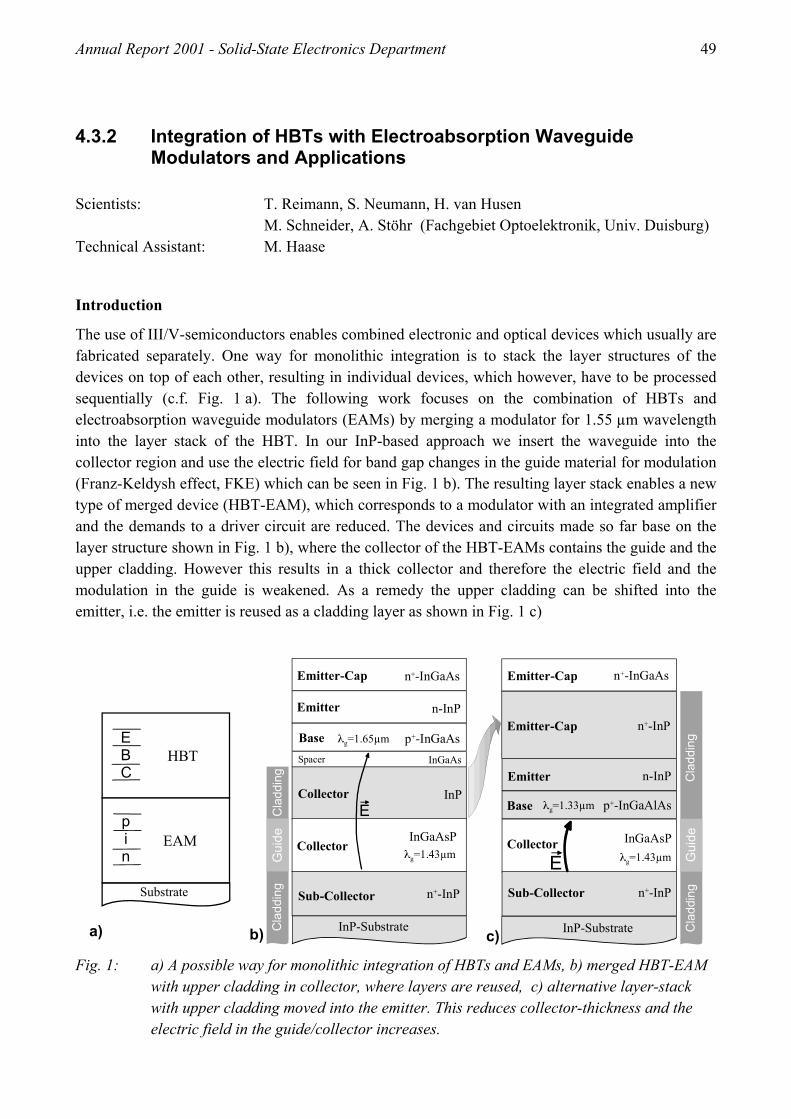
Annual Report 2001 - Solid-State Electronics Department 49
4.3.2 Integration of HBTs with Electroabsorption Waveguide Modulators and Applications
Scientists: T. Reimann, S. Neumann, H. van Husen M. Schneider, A. Stöhr (Fachgebiet Optoelektronik, Univ. Duisburg) Technical Assistant: M. Haase Introduction
The use of III/V-semiconductors enables combined electronic and optical devices which usually are fabricated separately. One way for monolithic integration is to stack the layer structures of the devices on top of each other, resulting in individual devices, which however, have to be processed sequentially (c.f. Fig. 1 a). The following work focuses on the combination of HBTs and electroabsorption waveguide modulators (EAMs) by merging a modulator for 1.55 µm wavelength into the layer stack of the HBT. In our InP-based approach we insert the waveguide into the collector region and use the electric field for band gap changes in the guide material for modulation (Franz-Keldysh effect, FKE) which can be seen in Fig. 1 b). The resulting layer stack enables a new type of merged device (HBT-EAM), which corresponds to a modulator with an integrated amplifier and the demands to a driver circuit are reduced. The devices and circuits made so far base on the layer structure shown in Fig. 1 b), where the collector of the HBT-EAMs contains the guide and the upper cladding. However this results in a thick collector and therefore the electric field and the modulation in the guide is weakened. As a remedy the upper cladding can be shifted into the emitter, i.e. the emitter is reused as a cladding layer as shown in Fig. 1 c)
Cla
ddin
gC
ladd
ing
Gui
de
n+-InP
p+-InGaAlAs
Emitter-Cap
Emitter-Cap
Base
n+-InP
InP-Substrate
Sub-Collector
Collector
n-InPEmitter
p+-InGaAsInGaAsSpacer
InP
InP-Substrate
Emitter-Cap
Emitter
Base
n+-InGaAs
n-InP
InGaAsP
Collector
Collector
Sub-Collector n+-InP
Cla
ddin
gC
ladd
ing
Gui
de
E
HBT
EAM
Substrate
a) b) c)
EBC
pin Eλg=1.43µm
InGaAsP
n+-InGaAs
λg=1.43µm
λg=1.65µm
λg=1.33µm
Fig. 1: a) A possible way for monolithic integration of HBTs and EAMs, b) merged HBT-EAM
with upper cladding in collector, where layers are reused, c) alternative layer-stack with upper cladding moved into the emitter. This reduces collector-thickness and the electric field in the guide/collector increases.
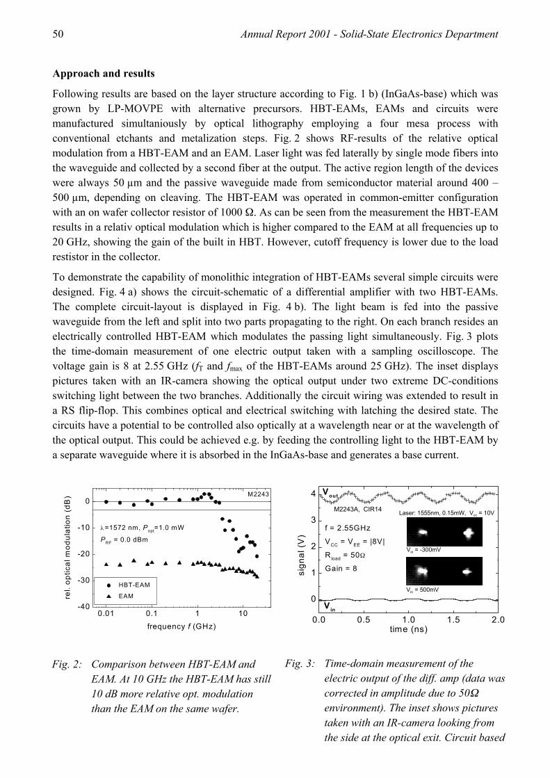
50 Annual Report 2001 - Solid-State Electronics Department
0.01 0.1 1 10-40
-30
-20
-10
0M2243
λ =1572 nm, Popt=1.0 mW
PRF = 0.0 dBm
HBT-EAM
EAMrel.
optic
al m
odul
atio
n (d
B)
frequency f (GHz)
Fig. 2: Comparison between HBT-EAM and EAM. At 10 GHz the HBT-EAM has still 10 dB more relative opt. modulation than the EAM on the same wafer.
Approach and results
Following results are based on the layer structure according to Fig. 1 b) (InGaAs-base) which was grown by LP-MOVPE with alternative precursors. HBT-EAMs, EAMs and circuits were manufactured simultaniously by optical lithography employing a four mesa process with conventional etchants and metalization steps. Fig. 2 shows RF-results of the relative optical modulation from a HBT-EAM and an EAM. Laser light was fed laterally by single mode fibers into the waveguide and collected by a second fiber at the output. The active region length of the devices were always 50 µm and the passive waveguide made from semiconductor material around 400 – 500 µm, depending on cleaving. The HBT-EAM was operated in common-emitter configuration with an on wafer collector resistor of 1000 Ω. As can be seen from the measurement the HBT-EAM results in a relativ optical modulation which is higher compared to the EAM at all frequencies up to 20 GHz, showing the gain of the built in HBT. However, cutoff frequency is lower due to the load restistor in the collector.
To demonstrate the capability of monolithic integration of HBT-EAMs several simple circuits were designed. Fig. 4 a) shows the circuit-schematic of a differential amplifier with two HBT-EAMs. The complete circuit-layout is displayed in Fig. 4 b). The light beam is fed into the passive waveguide from the left and split into two parts propagating to the right. On each branch resides an electrically controlled HBT-EAM which modulates the passing light simultaneously. Fig. 3 plots the time-domain measurement of one electric output taken with a sampling oscilloscope. The voltage gain is 8 at 2.55 GHz (fT and fmax of the HBT-EAMs around 25 GHz). The inset displays pictures taken with an IR-camera showing the optical output under two extreme DC-conditions switching light between the two branches. Additionally the circuit wiring was extended to result in a RS flip-flop. This combines optical and electrical switching with latching the desired state. The circuits have a potential to be controlled also optically at a wavelength near or at the wavelength of the optical output. This could be achieved e.g. by feeding the controlling light to the HBT-EAM by a separate waveguide where it is absorbed in the InGaAs-base and generates a base current.
0.0 0.5 1.0 1.5 2.0
0
1
2
3
4
Vin
Vout
f = 2.55GHz
VCC = VEE = |8V|
Rload = 50Ω
Gain = 8
sign
al (V
)
time (ns)
Vin = 500mV
Vin = -300mV
M2243A, CIR14 Laser: 1555nm, 0.15mW, Vcc = 10V
Fig. 3: Time-domain measurement of the electric output of the diff. amp (data was corrected in amplitude due to 50Ω environment). The inset shows pictures taken with an IR-camera looking from the side at the optical exit. Circuit based
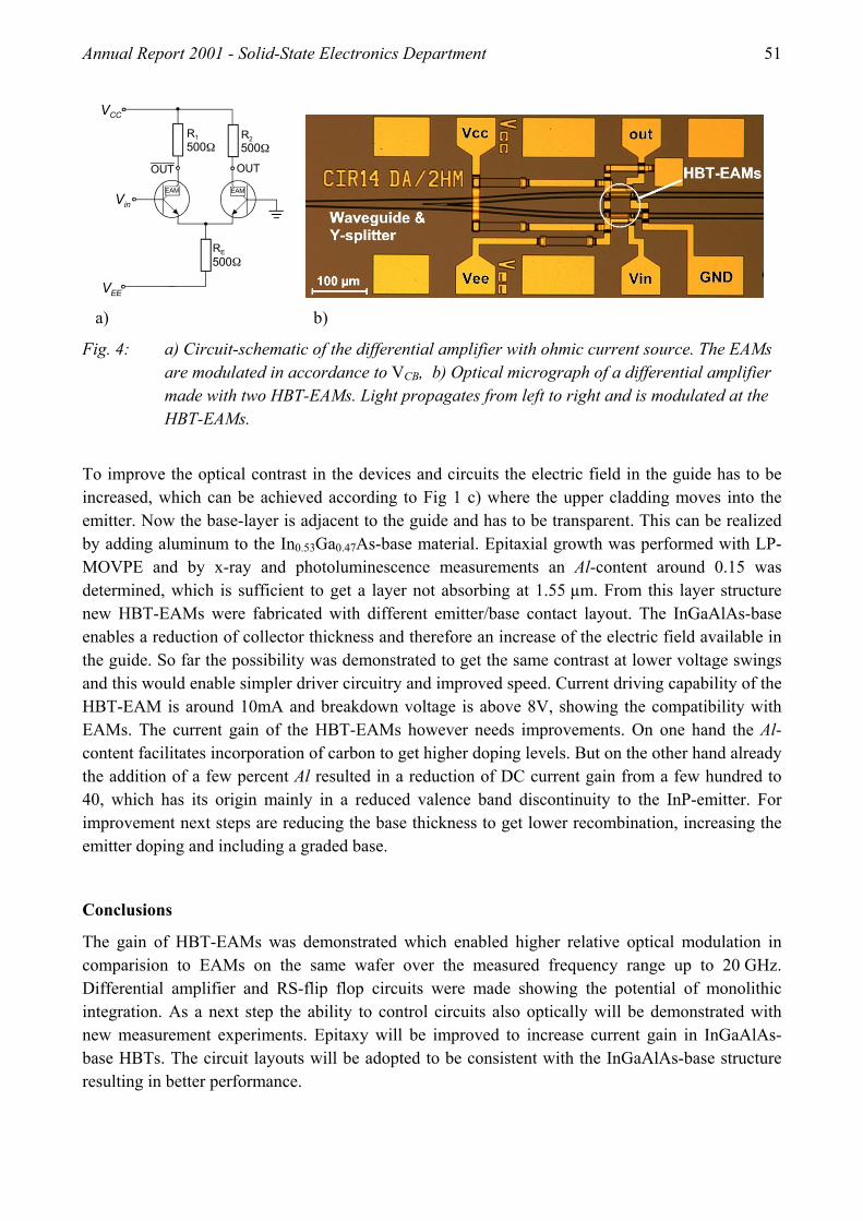
Annual Report 2001 - Solid-State Electronics Department 51
R1
EAM EAM
R2500Ω 500Ω
OUTOUT
RE
500Ω
Vin
VCC
VEE a) b)
Fig. 4: a) Circuit-schematic of the differential amplifier with ohmic current source. The EAMs are modulated in accordance to VCB, b) Optical micrograph of a differential amplifier made with two HBT-EAMs. Light propagates from left to right and is modulated at the HBT-EAMs.
To improve the optical contrast in the devices and circuits the electric field in the guide has to be increased, which can be achieved according to Fig 1 c) where the upper cladding moves into the emitter. Now the base-layer is adjacent to the guide and has to be transparent. This can be realized by adding aluminum to the In0.53Ga0.47As-base material. Epitaxial growth was performed with LP-MOVPE and by x-ray and photoluminescence measurements an Al-content around 0.15 was determined, which is sufficient to get a layer not absorbing at 1.55 µm. From this layer structure new HBT-EAMs were fabricated with different emitter/base contact layout. The InGaAlAs-base enables a reduction of collector thickness and therefore an increase of the electric field available in the guide. So far the possibility was demonstrated to get the same contrast at lower voltage swings and this would enable simpler driver circuitry and improved speed. Current driving capability of the HBT-EAM is around 10mA and breakdown voltage is above 8V, showing the compatibility with EAMs. The current gain of the HBT-EAMs however needs improvements. On one hand the Al-content facilitates incorporation of carbon to get higher doping levels. But on the other hand already the addition of a few percent Al resulted in a reduction of DC current gain from a few hundred to 40, which has its origin mainly in a reduced valence band discontinuity to the InP-emitter. For improvement next steps are reducing the base thickness to get lower recombination, increasing the emitter doping and including a graded base.
Conclusions
The gain of HBT-EAMs was demonstrated which enabled higher relative optical modulation in comparision to EAMs on the same wafer over the measured frequency range up to 20 GHz. Differential amplifier and RS-flip flop circuits were made showing the potential of monolithic integration. As a next step the ability to control circuits also optically will be demonstrated with new measurement experiments. Epitaxy will be improved to increase current gain in InGaAlAs-base HBTs. The circuit layouts will be adopted to be consistent with the InGaAlAs-base structure resulting in better performance.
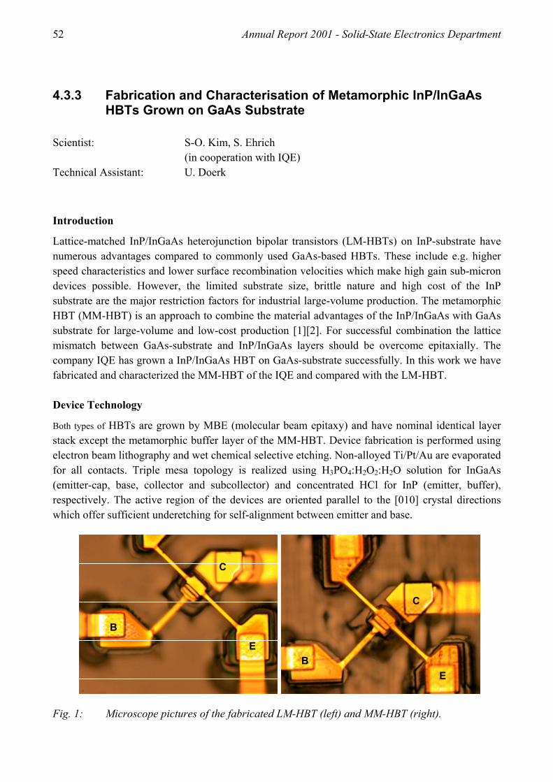
52 Annual Report 2001 - Solid-State Electronics Department
4.3.3 Fabrication and Characterisation of Metamorphic InP/InGaAs HBTs Grown on GaAs Substrate
Scientist: S-O. Kim, S. Ehrich (in cooperation with IQE) Technical Assistant: U. Doerk
Introduction
Lattice-matched InP/InGaAs heterojunction bipolar transistors (LM-HBTs) on InP-substrate have numerous advantages compared to commonly used GaAs-based HBTs. These include e.g. higher speed characteristics and lower surface recombination velocities which make high gain sub-micron devices possible. However, the limited substrate size, brittle nature and high cost of the InP substrate are the major restriction factors for industrial large-volume production. The metamorphic HBT (MM-HBT) is an approach to combine the material advantages of the InP/InGaAs with GaAs substrate for large-volume and low-cost production [1][2]. For successful combination the lattice mismatch between GaAs-substrate and InP/InGaAs layers should be overcome epitaxially. The company IQE has grown a InP/InGaAs HBT on GaAs-substrate successfully. In this work we have fabricated and characterized the MM-HBT of the IQE and compared with the LM-HBT. Device Technology
Both types of HBTs are grown by MBE (molecular beam epitaxy) and have nominal identical layer stack except the metamorphic buffer layer of the MM-HBT. Device fabrication is performed using electron beam lithography and wet chemical selective etching. Non-alloyed Ti/Pt/Au are evaporated for all contacts. Triple mesa topology is realized using H3PO4:H2O2:H2O solution for InGaAs (emitter-cap, base, collector and subcollector) and concentrated HCl for InP (emitter, buffer), respectively. The active region of the devices are oriented parallel to the [010] crystal directions which offer sufficient underetching for self-alignment between emitter and base.
Fig. 1: Microscope pictures of the fabricated LM-HBT (left) and MM-HBT (right).
B
E
C
BE
C
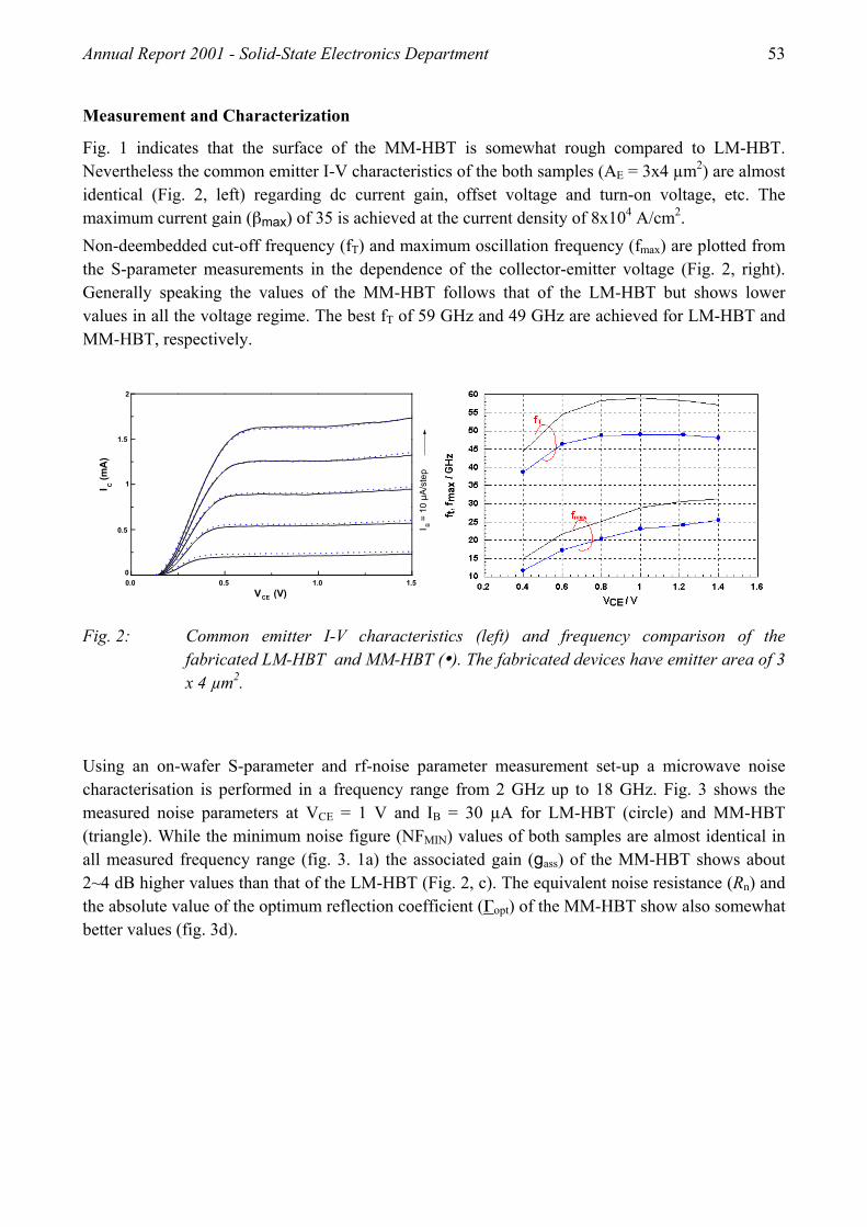
Annual Report 2001 - Solid-State Electronics Department 53
Measurement and Characterization
Fig. 1 indicates that the surface of the MM-HBT is somewhat rough compared to LM-HBT. Nevertheless the common emitter I-V characteristics of the both samples (AE = 3x4 µm2) are almost identical (Fig. 2, left) regarding dc current gain, offset voltage and turn-on voltage, etc. The maximum current gain (βmax) of 35 is achieved at the current density of 8x10⁴ A/cm2. Non-deembedded cut-off frequency (fT) and maximum oscillation frequency (fmax) are plotted from the S-parameter measurements in the dependence of the collector-emitter voltage (Fig. 2, right). Generally speaking the values of the MM-HBT follows that of the LM-HBT but shows lower values in all the voltage regime. The best fT of 59 GHz and 49 GHz are achieved for LM-HBT and MM-HBT, respectively.
Fig. 2: Common emitter I-V characteristics (left) and frequency comparison of the fabricated LM-HBT and MM-HBT (•). The fabricated devices have emitter area of 3 x 4 µm2.
Using an on-wafer S-parameter and rf-noise parameter measurement set-up a microwave noise characterisation is performed in a frequency range from 2 GHz up to 18 GHz. Fig. 3 shows the measured noise parameters at VCE = 1 V and IB = 30 µA for LM-HBT (circle) and MM-HBT (triangle). While the minimum noise figure (NFMIN) values of both samples are almost identical in all measured frequency range (fig. 3. 1a) the associated gain (gass) of the MM-HBT shows about 2~4 dB higher values than that of the LM-HBT (Fig. 2, c). The equivalent noise resistance (Rn) and the absolute value of the optimum reflection coefficient (Γopt) of the MM-HBT show also somewhat better values (fig. 3d).
0.0 0.5 1.0 1.50
2
1.5
1
0.5 I B = 1
0 µA
/ste
p
I C (mA
)
VCE (V)
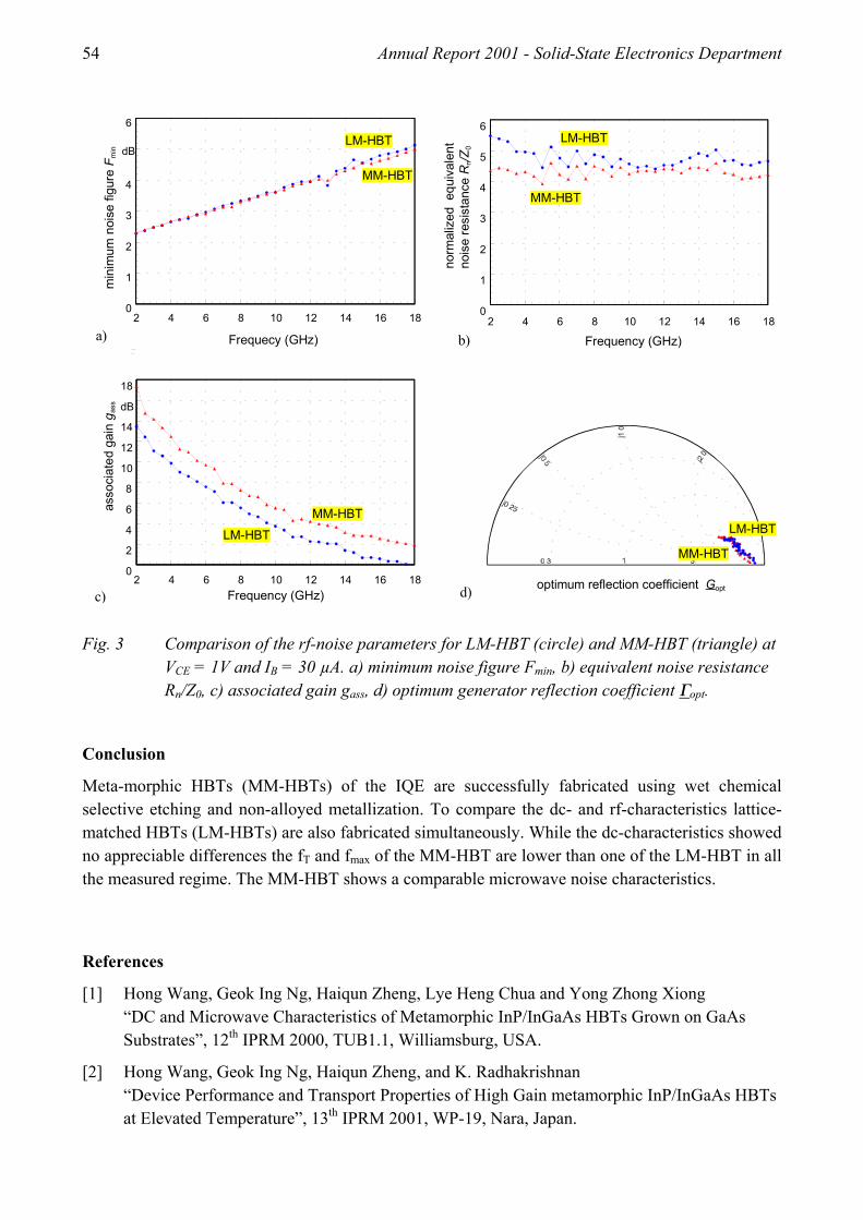
54 Annual Report 2001 - Solid-State Electronics Department
Fig. 3 Comparison of the rf-noise parameters for LM-HBT (circle) and MM-HBT (triangle) at
VCE = 1V and IB = 30 µA. a) minimum noise figure Fmin, b) equivalent noise resistance Rn/Z0, c) associated gain gass, d) optimum generator reflection coefficient Γopt.
Conclusion
Meta-morphic HBTs (MM-HBTs) of the IQE are successfully fabricated using wet chemical selective etching and non-alloyed metallization. To compare the dc- and rf-characteristics lattice-matched HBTs (LM-HBTs) are also fabricated simultaneously. While the dc-characteristics showed no appreciable differences the fT and fmax of the MM-HBT are lower than one of the LM-HBT in all the measured regime. The MM-HBT shows a comparable microwave noise characteristics. References
[1] Hong Wang, Geok Ing Ng, Haiqun Zheng, Lye Heng Chua and Yong Zhong Xiong “DC and Microwave Characteristics of Metamorphic InP/InGaAs HBTs Grown on GaAs Substrates”, 12th IPRM 2000, TUB1.1, Williamsburg, USA.
[2] Hong Wang, Geok Ing Ng, Haiqun Zheng, and K. Radhakrishnan “Device Performance and Transport Properties of High Gain metamorphic InP/InGaAs HBTs at Elevated Temperature”, 13th IPRM 2001, WP-19, Nara, Japan.
Frequecy (GHz)
min
imum
noi
se fi
gure
Fm
in
2 4 6 8 10 12 14 16 180
1
2
3
4
dB
6
2 4 6 8 10 12 14 16 180
1
2
3
4
5
6
Frequency (GHz)
norm
aliz
ed e
quiv
alen
t no
ise
resi
stan
ce R
n/Z0
0
2
4
6
8
10
12
14
dB
18
Frequency (GHz)2 4 6 8 10 12 14 16 18
asso
ciat
ed g
ain
g ass
optimum reflection coefficient Gopt
a) b)
c) d)
MM-HBT
MM-HBT
MM-HBT
LM-HBT
LM-HBT
LM-HBT
LM-HBT
MM-HBT
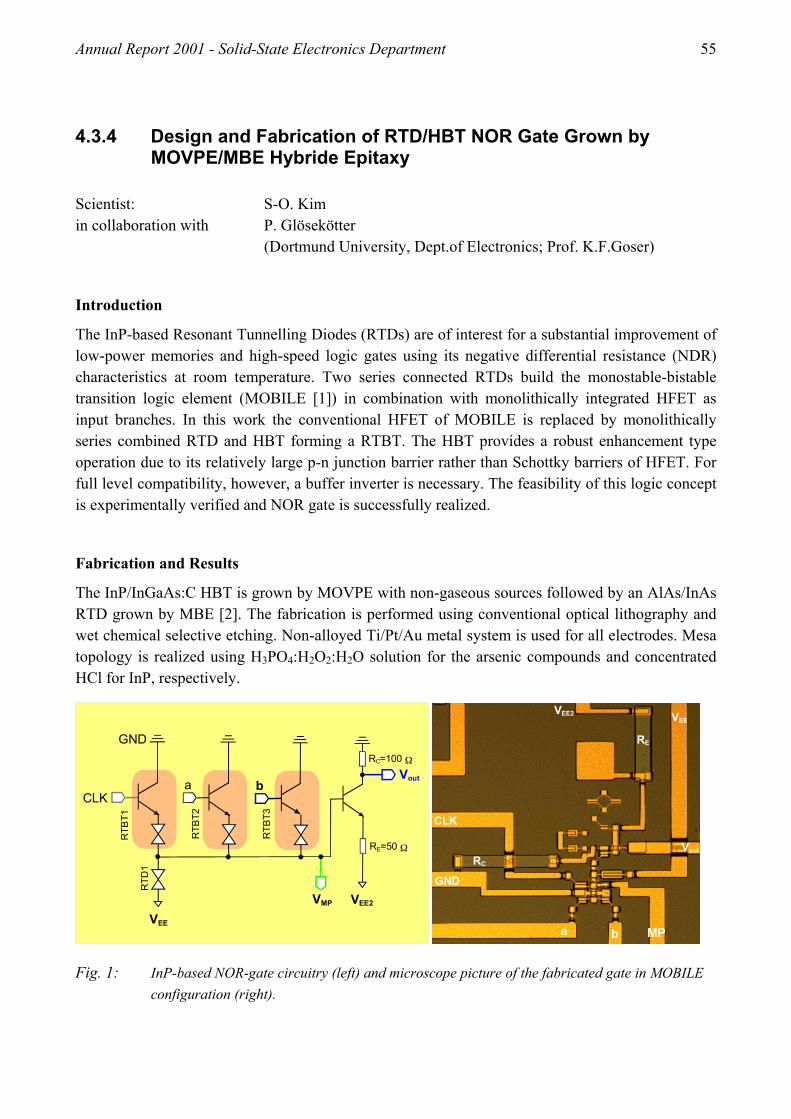
Annual Report 2001 - Solid-State Electronics Department 55
4.3.4 Design and Fabrication of RTD/HBT NOR Gate Grown by MOVPE/MBE Hybride Epitaxy
Scientist: S-O. Kim in collaboration with P. Glösekötter (Dortmund University, Dept.of Electronics; Prof. K.F.Goser) Introduction
The InP-based Resonant Tunnelling Diodes (RTDs) are of interest for a substantial improvement of low-power memories and high-speed logic gates using its negative differential resistance (NDR) characteristics at room temperature. Two series connected RTDs build the monostable-bistable transition logic element (MOBILE [1]) in combination with monolithically integrated HFET as input branches. In this work the conventional HFET of MOBILE is replaced by monolithically series combined RTD and HBT forming a RTBT. The HBT provides a robust enhancement type operation due to its relatively large p-n junction barrier rather than Schottky barriers of HFET. For full level compatibility, however, a buffer inverter is necessary. The feasibility of this logic concept is experimentally verified and NOR gate is successfully realized.
Fabrication and Results
The InP/InGaAs:C HBT is grown by MOVPE with non-gaseous sources followed by an AlAs/InAs RTD grown by MBE [2]. The fabrication is performed using conventional optical lithography and wet chemical selective etching. Non-alloyed Ti/Pt/Au metal system is used for all electrodes. Mesa topology is realized using H3PO4:H2O2:H2O solution for the arsenic compounds and concentrated HCl for InP, respectively.
Fig. 1: InP-based NOR-gate circuitry (left) and microscope picture of the fabricated gate in MOBILE configuration (right).
GN
D
CLK
a
bM
P VEE
VEE2
RC
RE
CLK
VEE
Vout
RE=50 Ω
a b
GND
VMP VEE2
RC=100 Ω
RTB
T1
RTB
T2
RTB
T3
RTD
1
GND
CLK
VEE
Vout
RE
RC
VEE2
a b MP
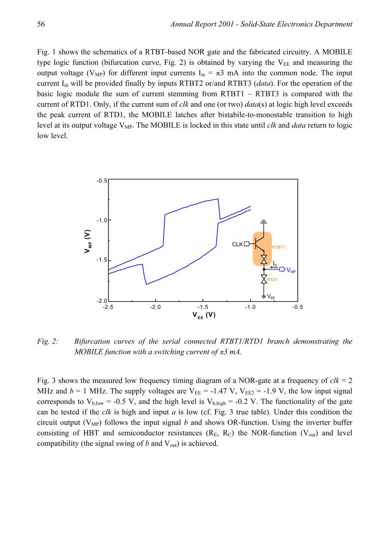
56 Annual Report 2001 - Solid-State Electronics Department
Fig. 1 shows the schematics of a RTBT-based NOR gate and the fabricated circuitry. A MOBILE type logic function (bifurcation curve, Fig. 2) is obtained by varying the VEE and measuring the output voltage (VMP) for different input currents Iin = ±3 mA into the common node. The input current Iin will be provided finally by inputs RTBT2 or/and RTBT3 (data). For the operation of the basic logic module the sum of current stemming from RTBT1 – RTBT3 is compared with the current of RTD1. Only, if the current sum of clk and one (or two) data(s) at logic high level exceeds the peak current of RTD1, the MOBILE latches after bistabile-to-monostable transition to high level at its output voltage VMP. The MOBILE is locked in this state until clk and data return to logic low level.
Fig. 2: Bifurcation curves of the serial connected RTBT1/RTD1 branch demonstrating the MOBILE function with a switching current of ±3 mA.
Fig. 3 shows the measured low frequency timing diagram of a NOR-gate at a frequency of clk = 2 MHz and b = 1 MHz. The supply voltages are VEE = -1.47 V, VEE2 = -1.9 V, the low input signal corresponds to Vb,low = -0.5 V, and the high level is Vb,high = -0.2 V. The functionality of the gate can be tested if the clk is high and input a is low (cf. Fig. 3 true table). Under this condition the circuit output (VMP) follows the input signal b and shows OR-function. Using the inverter buffer consisting of HBT and semiconductor resistances (RE, RC) the NOR-function (Vout) and level compatibility (the signal swing of b and Vout) is achieved.
-2.5 -2.0 -1.5 -1.0 -0.5
-0.5
-1.0
-1.5
-2.0
VM
P (V
)
VEE (V)
CLK
VEE
VMP
Iin
RTBT1
RTD1
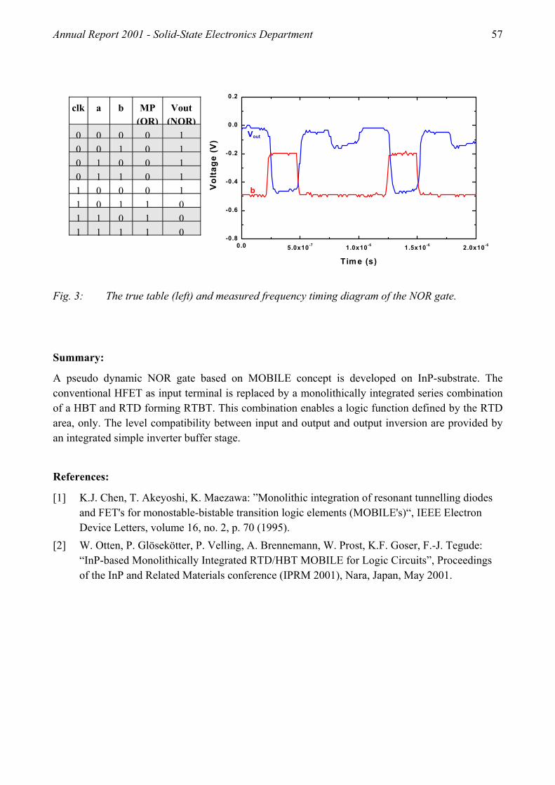
Annual Report 2001 - Solid-State Electronics Department 57
Fig. 3: The true table (left) and measured frequency timing diagram of the NOR gate.
Summary:
A pseudo dynamic NOR gate based on MOBILE concept is developed on InP-substrate. The conventional HFET as input terminal is replaced by a monolithically integrated series combination of a HBT and RTD forming RTBT. This combination enables a logic function defined by the RTD area, only. The level compatibility between input and output and output inversion are provided by an integrated simple inverter buffer stage.
References:
[1] K.J. Chen, T. Akeyoshi, K. Maezawa: ”Monolithic integration of resonant tunnelling diodes and FET's for monostable-bistable transition logic elements (MOBILE's)“, IEEE Electron Device Letters, volume 16, no. 2, p. 70 (1995).
[2] W. Otten, P. Glösekötter, P. Velling, A. Brennemann, W. Prost, K.F. Goser, F.-J. Tegude: “InP-based Monolithically Integrated RTD/HBT MOBILE for Logic Circuits”, Proceedings of the InP and Related Materials conference (IPRM 2001), Nara, Japan, May 2001.
0.0 5.0x10⁻⁷ 1.0x10⁻⁶ 1.5x10⁻⁶ 2.0x10⁻⁶-0.8
-0.6
-0.4
-0.2
0.0
0.2
Vol
tage
(V)
T ime (s)
Vout
b
clk a b MP (OR)
Vout (NOR)
0 0 0 0 1 0 0 1 0 1 0 1 0 0 1 0 1 1 0 1 1 0 0 0 1 1 0 1 1 0 1 1 0 1 0 1 1 1 1 0
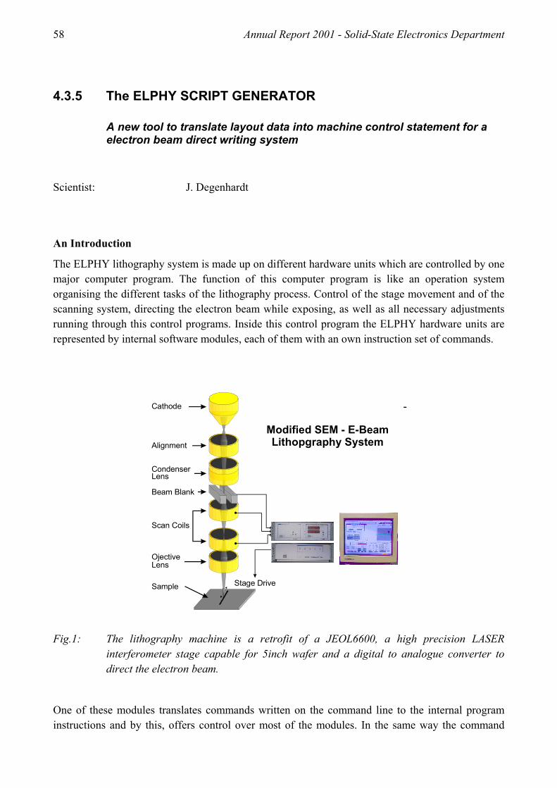
58 Annual Report 2001 - Solid-State Electronics Department
4.3.5 The ELPHY SCRIPT GENERATOR
A new tool to translate layout data into machine control statement for a electron beam direct writing system
Scientist: J. Degenhardt
An Introduction
The ELPHY lithography system is made up on different hardware units which are controlled by one major computer program. The function of this computer program is like an operation system organising the different tasks of the lithography process. Control of the stage movement and of the scanning system, directing the electron beam while exposing, as well as all necessary adjustments running through this control programs. Inside this control program the ELPHY hardware units are represented by internal software modules, each of them with an own instruction set of commands.
Cathode
Alignment
CondenserLens
Beam Blank
Scan Coils
LensOjective
Sample Stage Drive
Modified SEM - E-BeamLithopgraphy System
Fig.1: The lithography machine is a retrofit of a JEOL6600, a high precision LASER interferometer stage capable for 5inch wafer and a digital to analogue converter to direct the electron beam.
One of these modules translates commands written on the command line to the internal program instructions and by this, offers control over most of the modules. In the same way the command
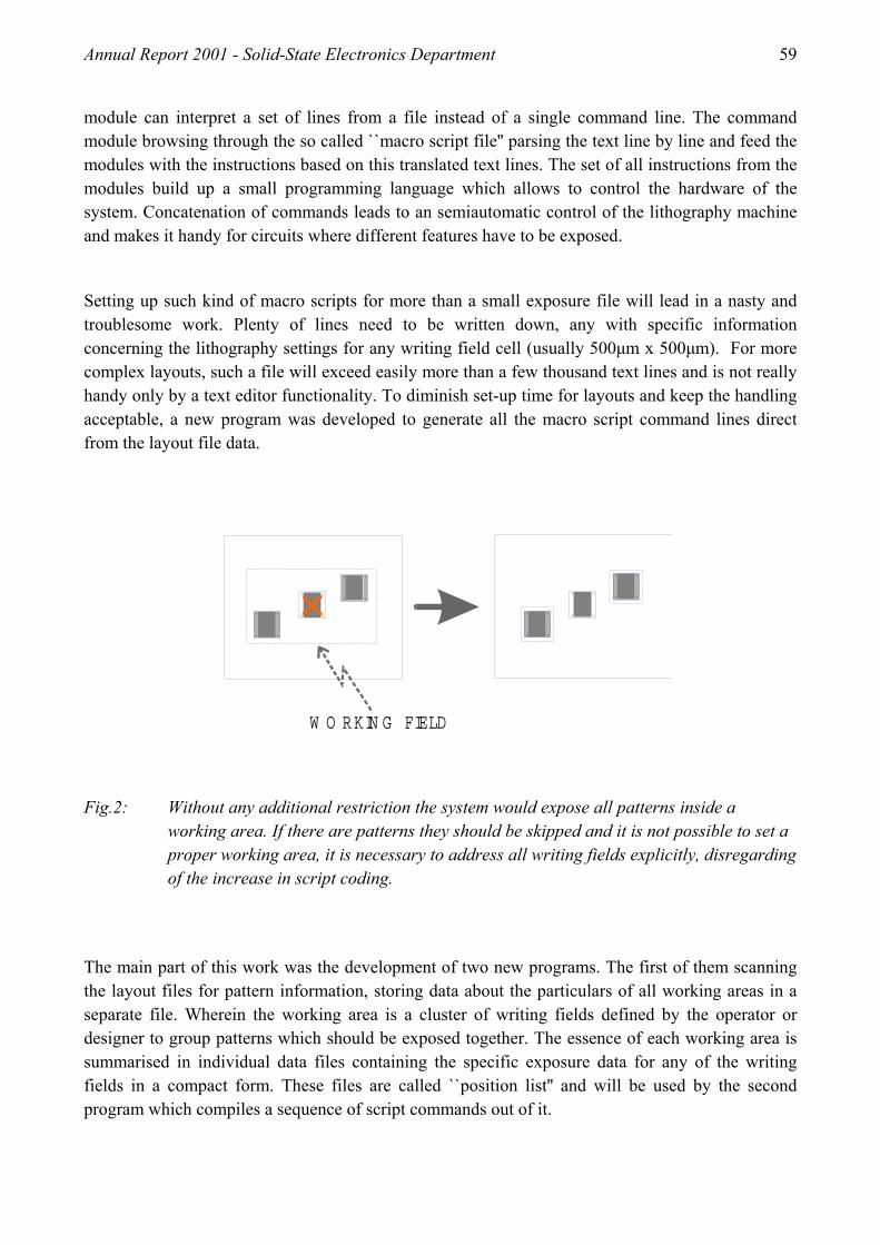
Annual Report 2001 - Solid-State Electronics Department 59
module can interpret a set of lines from a file instead of a single command line. The command module browsing through the so called ``macro script file'' parsing the text line by line and feed the modules with the instructions based on this translated text lines. The set of all instructions from the modules build up a small programming language which allows to control the hardware of the system. Concatenation of commands leads to an semiautomatic control of the lithography machine and makes it handy for circuits where different features have to be exposed.
Setting up such kind of macro scripts for more than a small exposure file will lead in a nasty and troublesome work. Plenty of lines need to be written down, any with specific information concerning the lithography settings for any writing field cell (usually 500µm х 500µm). For more complex layouts, such a file will exceed easily more than a few thousand text lines and is not really handy only by a text editor functionality. To diminish set-up time for layouts and keep the handling acceptable, a new program was developed to generate all the macro script command lines direct from the layout file data.
Fig.2: Without any additional restriction the system would expose all patterns inside a working area. If there are patterns they should be skipped and it is not possible to set a proper working area, it is necessary to address all writing fields explicitly, disregarding of the increase in script coding.
The main part of this work was the development of two new programs. The first of them scanning the layout files for pattern information, storing data about the particulars of all working areas in a separate file. Wherein the working area is a cluster of writing fields defined by the operator or designer to group patterns which should be exposed together. The essence of each working area is summarised in individual data files containing the specific exposure data for any of the writing fields in a compact form. These files are called ``position list'' and will be used by the second program which compiles a sequence of script commands out of it.
W O RKIN G FIELD

60 Annual Report 2001 - Solid-State Electronics Department
Table 1: position list
WF = 500.00 BASE = (0.00, 0.00) # This is the position data file for the power devices # The power transistors are arranged in rows to 2, 3 and 5 lines # where each line consist of 11 transistor fields per die. # P0-11-11 / Mon Jun 21 17:54:48 2001 1000.00 1000.00 1 1 500.00 500.00 4 # position of glb alignment mark for 4000.00 4000.00 1 1 0.00 0.00 16
It has different advantage to split this routine into two programs. The writing field data gathered from the layout file and stored in plain text files can be modified by a simple text editor. Because the data are in a compact presentation one can change the settings and/or positions of a cluster of writing fields by a few text lines (see table 1).
After generating the position list, the second program uses these data to generate a sequence of program module instructions (see table 2). The sequence includes the definition of the writing fields to be exposed, the initialisation of automatic mark alignment and commands to activate all settings. Parts of these commands are linked to other routines which contain sets of typical instruction sequences.
Table 2: macro sequence
! This is the process control file : D0-11-11 ! The file was compiled on : Tue Aug 8 11:16:42 2001 OpenDatabase(FILEDB) ViewStructure(STRUCTURE) !***************************************! SetWorkingArea(1000.00, 1000.00, 1500.00, 1500.00) ViewStructure(STRUCTURE) DriveUVAbs(1250.00, 1250.00) Call(RSTSWP) Call(EXPOSURE) !***************************************!
All these individual files for any of the writing field positions have an index which identifies them for a certain working area. After a general machine set-up and settings for the expose parameter, these file will be call one after the other to initialise the exposure sequence for the individual areas on the wafer, later during the exposure process.
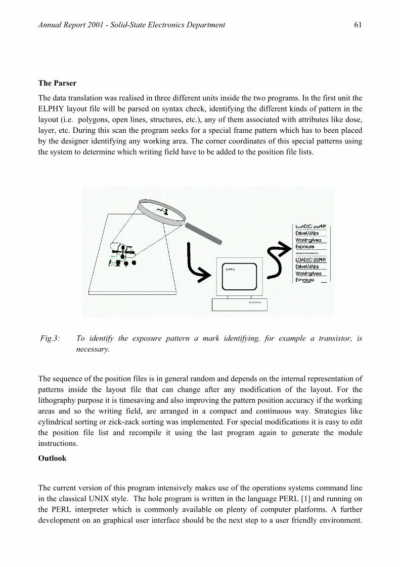
Annual Report 2001 - Solid-State Electronics Department 61
The Parser
The data translation was realised in three different units inside the two programs. In the first unit the ELPHY layout file will be parsed on syntax check, identifying the different kinds of pattern in the layout (i.e. polygons, open lines, structures, etc.), any of them associated with attributes like dose, layer, etc. During this scan the program seeks for a special frame pattern which has to been placed by the designer identifying any working area. The corner coordinates of this special patterns using the system to determine which writing field have to be added to the position file lists.
Fig.3: To identify the exposure pattern a mark identifying, for example a transistor, is necessary.
The sequence of the position files is in general random and depends on the internal representation of patterns inside the layout file that can change after any modification of the layout. For the lithography purpose it is timesaving and also improving the pattern position accuracy if the working areas and so the writing field, are arranged in a compact and continuous way. Strategies like cylindrical sorting or zick-zack sorting was implemented. For special modifications it is easy to edit the position file list and recompile it using the last program again to generate the module instructions.
Outlook
The current version of this program intensively makes use of the operations systems command line in the classical UNIX style. The hole program is written in the language PERL [1] and running on the PERL interpreter which is commonly available on plenty of computer platforms. A further development on an graphical user interface should be the next step to a user friendly environment.
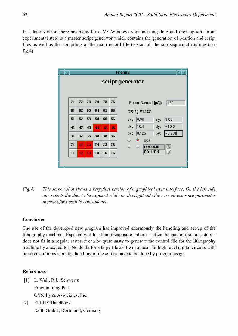
62 Annual Report 2001 - Solid-State Electronics Department
In a later version there are plans for a MS-Windows version using drag and drop option. In an experimental state is a master script generator which contains the generation of position and script files as well as the compiling of the main record file to start all the sub sequential routines.(see fig.4)
Fig.4: This screen shot shows a very first version of a graphical user interface. On the left side one selects the dies to be exposed while on the right side the current exposure parameter appears for possible adjustments.
Conclusion
The use of the developed new program has improved enormously the handling and set-up of the lithography machine . Especially, if location of exposure pattern -- often the gate of the transistors –does not fit in a regular raster, it can be quite nasty to generate the control file for the lithography machine by a text editor. No doubt for a large file as it will appear for high level digital circuits with hundreds of transistors the handling of these files have to be done by program usage.
References:
[1] L. Wall, R.L. Schwartz Programming Perl O’Reilly & Associates, Inc.
[2] ELPHY Handbook Raith GmbH, Dortmund, Germany
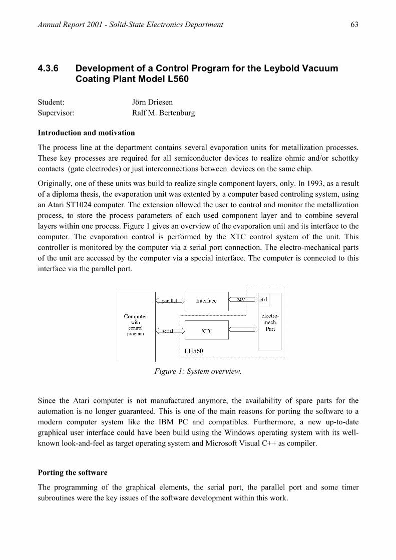
Annual Report 2001 - Solid-State Electronics Department 63
4.3.6 Development of a Control Program for the Leybold Vacuum Coating Plant Model L560
Student: Jörn Driesen Supervisor: Ralf M. Bertenburg Introduction and motivation
The process line at the department contains several evaporation units for metallization processes. These key processes are required for all semiconductor devices to realize ohmic and/or schottky contacts (gate electrodes) or just interconnections between devices on the same chip.
Originally, one of these units was build to realize single component layers, only. In 1993, as a result of a diploma thesis, the evaporation unit was extented by a computer based controling system, using an Atari ST1024 computer. The extension allowed the user to control and monitor the metallization process, to store the process parameters of each used component layer and to combine several layers within one process. Figure 1 gives an overview of the evaporation unit and its interface to the computer. The evaporation control is performed by the XTC control system of the unit. This controller is monitored by the computer via a serial port connection. The electro-mechanical parts of the unit are accessed by the computer via a special interface. The computer is connected to this interface via the parallel port.
Figure 1: System overview.
Since the Atari computer is not manufactured anymore, the availability of spare parts for the automation is no longer guaranteed. This is one of the main reasons for porting the software to a modern computer system like the IBM PC and compatibles. Furthermore, a new up-to-date graphical user interface could have been build using the Windows operating system with its well-known look-and-feel as target operating system and Microsoft Visual C++ as compiler.
Porting the software
The programming of the graphical elements, the serial port, the parallel port and some timer subroutines were the key issues of the software development within this work.
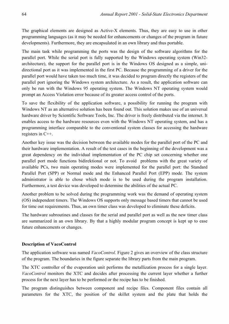
64 Annual Report 2001 - Solid-State Electronics Department
The graphical elements are designed as Active-X elements. Thus, they are easy to use in other programming languages (as it may be needed for enhancements or changes of the program in future developments). Furthermore, they are encapsulated in an own library and thus portable.
The main task while programming the ports was the design of the software algorithms for the parallel port. While the serial port is fully supported by the Windows operating system (Win32-architecture), the support for the parallel port is in the Windows OS designed as a simple, uni-directional port as it was implemented in the first PC. Because the programming of a driver for the parallel port would have taken too much time, it was decided to program directly the registers of the parallel port ignoring the Windows system architecture. As a result, the application software can only be run with the Windows 95 operating system. The Windows NT operating system would prompt an Access Violation error because of its greater access control of the ports.
To save the flexibility of the application software, a possibility for running the program with Windows NT as an alternative solution has been found out. This solution makes use of an universal hardware driver by Scientific Software Tools, Inc. The driver is freely distributed via the internet. It enables access to the hardware resources even with the Windows NT operating system, and has a programming interface comparable to the conventional system classes for accessing the hardware registers in C++.
Another key issue was the decision between the available modes for the parallel port of the PC and their hardware implementation. A result of the test cases in the beginning of the development was a great dependency on the individual implementation of the PC chip set concerning whether one parallel port mode functions bidirektional or not. To avoid problems with the great variety of available PCs, two main operating modes were implemented for the parallel port: the Standard Parallel Port (SPP) or Normal mode and the Enhanced Parallel Port (EPP) mode. The system administrator is able to chose which mode is to be used during the program installation. Furthermore, a test device was developed to determine the abilities of the actual PC.
Another problem to be solved during the programming work was the demand of operating system (OS) independent timers. The Windows OS supports only message based timers that cannot be used for time out requirements. Thus, an own timer class was developed to eliminate these deficits.
The hardware subroutines and classes for the serial and parallel port as well as the new timer class are summarized in an own library. By that a highly modular program concept is kept up to ease future enhancements or changes.
Description of VacoControl
The application software was named VacoControl. Figure 2 gives an overview of the class structure of the program. The boundaries in the figure separate the library parts from the main program.
The XTC controller of the evaporation unit performs the metallization process for a single layer. VacoControl monitors the XTC and decides after processing the current layer whether a further process for the next layer has to be performed or the recipe has to be finished.
The program distinguishes between component and recipe files. Component files contain all parameters for the XTC, the position of the skillet system and the plate that holds the
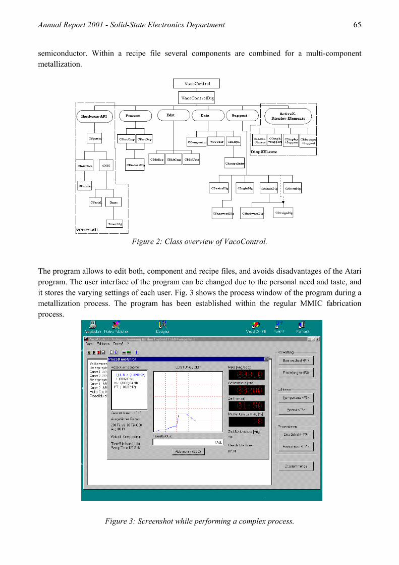
Annual Report 2001 - Solid-State Electronics Department 65
semiconductor. Within a recipe file several components are combined for a multi-component metallization.
Figure 2: Class overview of VacoControl.
The program allows to edit both, component and recipe files, and avoids disadvantages of the Atari program. The user interface of the program can be changed due to the personal need and taste, and it stores the varying settings of each user. Fig. 3 shows the process window of the program during a metallization process. The program has been established within the regular MMIC fabrication process.
Figure 3: Screenshot while performing a complex process.

66 Annual Report 2001 - Solid-State Electronics Department
References:
[1] Leybold Technical Manuals, 1989.
[2] Microsoft Microsoft Windows 95 – Technical Reference. Microsoft Press, 1996.
[3] Craig Peacock Beyond Logic: Internet Sites for Interfacing the PC Computer. http://www.beyondlogic.org, 2000.
[4] Christian Spiska Automatisierung des Aufdampfprozesses zur Herstellung von Mehrlagen-Metallsystemen in einem Leybold-Pumpstand LH560. Diploma thesis, University of Duisburg, Germany, 1993.
[5] Scientific Software Tools, Inc. Freeware port driver for Windows 95/98/NT. http://www.sstnet.com, 2000.
Annual Report 2001 - Solid-State Electronics Department 67
4.4 Conference Contributions
1. W. PROST LOCOM MEL-ARI NID Meeting, Plenary, Barcelona, 08.02.2001
2. W. PROST Speed-Index and Digital Circuit Applications of Si/SiGe Interband Tunnelling Diodes MEL-ARI NID Meeting, Working Group Devices, 08.02.2001
3. F.-J. TEGUDE Technologien und Komponenten für die Hochgeschwindigkeits-InP-Elektronik BMBF InP-Workshop, 02.04.01, Erlangen, Germany
4. W.PROST Tunnelling Diode Technology a) 31st IEEE International Symposium on Multiple-Valued Logic' (ISMVL 2001), 2001, Seminar at: a) NTT Photonics Laboratories, Atsugi, 10. Mai 2001 b) Sophia University, Tokyo, 11. Mai 2001 c) Nagoya University, Nagoya, 14. Mai 2001
5. S.SCHÜLLER, R.M.BERTENBURG, M.AGETHEN, A.BRENNEMANN, W.BROCKERHOFF, F.J.TEGUDE A New Consistent and Scalable PSPICE Model for Enhancement and Depletion-Type HFET '11th Conf. and Exhibition on Microwaves, Radio Communication and Electromagnetics Compatibility' (MIOP 2001), Stuttgart, FRG, 08.-10.05.01
6. W.PROST, U.AUER, J.DEGENHARDT, A.BRENNEMANN, C.PACHA1, K.F.GOSER1, F.-J.TEGUDE 1 Universität Dortmund, LS Bauelemente der Elektrotechnik
Technology of a Depth-2 Full-Adder Circuit using the InP RTD/HFET MOBILE Poster WP 26, '13th Int. Conf. on InP and Related Materials' (IPRM 2001), Nara, Japan 16.05.01.
7. W.OTTEN, P.GLÖSEKÖTTER1, P.VELLING, A.BRENNEMANN, W.PROST, K.F.GOSER1, F.-J.TEGUDE 1 Universität Dortmund, LS Bauelemente der Elektrotechnik
InP-based monolithically integrated RTD/HBT MOBILE for logic circuits Poster WP 27, '13th Int. Conf. on InP and Related Materials' (IPRM 2001), Nara, Japan 16.05.01.
8. T. REIMANN, M. SCHNEIDER1, P. VELLING, S. NEUMANN, M. AGETHEN, R. M. BERTENBURG, R. HEINZELMANN1, A. STÖHR1, D. JÄGER1, F.-J. TEGUDE 1): Gerhard-Mercator-Universität - GH Duisburg, Dept. of Optoelectronics
Integration of HBT and electroabsorption modulator based on a multifunctional layer design for 1,55 µm '13th Int. Conf. on InP and Related Materials' (IPRM 2001), Nara, Japan 16.05.01.
9. W.PROST, U.AUER, F.-J.TEGUDE, C.PACHA1, K.F.GOSER1, R.DUSCHL1, K.EBERL2, O.G.SCHMIDT1 (INVITED) 1 Universität Dortmund, LS Bauelemente der Elektrotechnik 2 Max-Planck Institut, Stuttgart, Germany
Tunnelling Diode Technology '31st IEEE International Symposium on Multiple-Valued Logic' (ISMVL 2001), IEEE Computer Society, Warshaw, May 21st, 2001
68 Annual Report 2001 - Solid-State Electronics Department
10. M.AGETHEN, S.SCHÜLLER, P.VELLING, W.BROCKERHOFF, F.J.TEGUDE Carbon Doped InP/InGaAs HBT: Consistent Small_Signal and RF-Noise Modelling and Characterization 'Workshop on Compound Semiconductor Devices and Circuits' (WOCSDICE 2001), Cagliari , Italy, 27.05.01 - 30.05.01
11. M. AGETHEN, S. SCHÜLLER, P. VELLING, W. BROCKERHOFF, F.-J. TEGUDE Consistent small signal and rf-noise parameter modeling of carbon doped InP/InGaAs HBT 'Microwave Theory and Technics Symposium' (MTTS), Phoenix, Arizona USA June 2001.
12. W.PROST, F.-J.TEGUDE Nanopartikel in epitaktischen Heterostrukturschichten Vorbereitungsseminar des "SFB 445 - Nano-Partikel aus der Gasphase: Entstehung, Struktur, Eigenschaften", Hirschegg, Klein-Walsertal, 26. Juni 2001.
13. F.OTTEN, U.AUER, F.E. KRUIS1, W.PROST, F.-J.TEGUDE, H.FISSAN1 1: Process- and Aerosol Measurement Technology Division, Gerhard-Mercator University Duisburg
Gas-Phase Generated Nanocrystals with Self-Adjusted Sub-µm Film Feature Size '43rd Electronic Materials Conference', June 27-29, 2001.
14. P. VELLING1, M. AGETHEN1, W. PROST, G. JANSSEN1, R. M. BERTENBURG1 AND F.J. TEGUDE An intrinsically coupled HBT/RTD device enabling an adjustable Peak-Current-Density 'Device Research Conference' (DRC), Notre Dame, USA, June 2001
15. P. VELLING1, S. NEUMANN, F. SCHULZE-KRAASCH2, M. AGETHEN1, W. PROST, G. JANSSEN1, R. M. BERTENBURG1 AND F.J. TEGUDE 1now with IPAG – Innovative Processing AG, Duisburg 2 Materials for Electrical Engineering, Gerhard-Mercator Universität Duisburg.
X-ray Analysis of InP/(InGa)As:C HBT and (InAl)As/(InGa)As RTD Structures Grown by LP-MOVPE Using Non-Gaseous-Sources '9th European Workshop on Metal-Organic Vaphor Phase Epitaxy and Related Growth Techniques' (EW-MOVPE), Wrexham, UK, June 2001
16. F.OTTEN, P.MUESCHENBORN1, A.TRAMPE1, S.NEUMANN, H.FISSAN1 1: Process- and Aerosol Measurement Technology Division, Gerhard-Mercator University Duisburg
Unipolar Aerosol Charger for Singly Charged Particles Between 3 to 1000 nm '2nd Asian Aerosol Conference', 02.-04.07.2001, Pusan, Korea (Poster)
17. F.OTTEN , W.GERBER1, F.E.KRUIS1, H.FISSAN1 1: Process- and Aerosol Measurement Technology Division, Gerhard-Mercator University Duisburg
Development of a Nanoparticle Precipitation and Characterization System 'International Symposium on “Nanoparticles: Aerosols and Materials”', 05.-06.07.2001, Pusan, Korea (Poster)
18. M.N.MIHAILA1, F.SCHEFFER2, C.HEEDT3, F.J.TEGUDE (INVITED) 1: National Institute of Microtechnology, Bucharest, Romania 2: ELMOS Semiconductor AG, Dortmund, Germany 3: Wacker Siltronic AG, Freiberg, Germany
Nonlinear Effects in the 1/f Noise of a 2D Electron Gas '9th Int. Federation of Automation and Control Symposium on Large Scale Systems', 19.07.01
Annual Report 2001 - Solid-State Electronics Department 69
19. C.PACHA1, W.PROST, F.-J.TEGUDE, R.THEWES2, K.GOSER1 (INVITED) 1 Universität Dortmund, LS Bauelemente der Elektrotechnik, 2 Infineon, München
Resonant Tunneling Device Logic: A Circuit Designer's Perspective '2001 European Conference on Circuit Theory and Design' (ECCTD'01), Helsinki, 28.-31. August 2001.
20. S.EHRICH, M.AGETHEN, R.M.BERTENBURG, A.BRENNEMANN, W.BROCKERHOFF, F.J.TEGUDE A Consistent and Scalable PSPICE Compound Semiconductor HFET Model for DC- and S-Parameter Simulation '9th GaAs Application Symposium' (GAAS 2001), London, U.K., 24.-25.09.01
21. T. REIMANN, M. SCHNEIDER1), S. NEUMANN, H. VAN HUSEN, A. STÖHR1), D. JÄGER1), F.-J. TEGUDE 1): Gerhard-Mercator-Universität - Duisburg, Dept. of Optoelectronics
Integration of Heterostrucutre Bipolartransisitors with Electroabsorption Waveguide Modulators and Applications '11th European Heterostructure Technology Workshop', (HETECH), 28.-30.10.01, Padova , Italy
22. W. PROST (INVITED) Digital Circuits '11th European Heterostructure Technology Workshop', (HETECH), 28.-30.10.01, Padova , Italy
23. S.EHRICH, M.AGETHEN, W.BROCKERHOFF, F.-J.TEGUDE RF- and Noise-Modeling of Semiconductor Devices based on InP 'ITG-Diskussionssitzung', IMST, Kamp-Lintfort, 23.-24.10.2001
70 Annual Report 2001 - Solid-State Electronics Department
4.5 Publications 1. U.AUER, W.PROST, F-J.TEGUDE, R.DUSCHL1, K.EBERL1
1 Max-Planck Institut, Stuttgart Low-Voltage MOBILE Logic Module Based on Si/SiGe Interband Tunnelling Diodes, Electron Device Letters, vol. 22, no. 5, pp.215-217, 2001.
2. W.PROST, U.AUER, J.DEGENHARDT, A.BRENNEMANN, C.PACHA1, K.F.GOSER1, F.-J.TEGUDE 1 Universität Dortmund, LS Bauelemente der Elektrotechnik
Technology of a Depth-2 Full-Adder Circuit using the InP RTD/HFET MOBILE Proc. '13th Int. Conf. on InP and Related Materials' (IPRM 2001), Nara, Japan, pp.228-231, May 2001.
3. W.OTTEN, P.GLÖSEKÖTTER1, P.VELLING, A.BRENNEMANN, W.PROST, K.F.GOSER1, F.-J.TEGUDE 1 Universität Dortmund, LS Bauelemente der Elektrotechnik
InP-based monolithically integrated RTD/HBT MOBILE for logic circuits Proc. '13th Int. Conf. on InP and Related Materials' (IPRM 2001), Nara, Japan, pp.232-235, May 2001.
4. T. REIMANN, M. SCHNEIDER1, P. VELLING, S. NEUMANN, M. AGETHEN, R. M. BERTENBURG, R. HEINZELMANN1, A. STÖHR1, D. JÄGER1, F.-J. TEGUDE 1): Gerhard-Mercator-Universität Duisburg, Dept. of Optoelectronics
Integration of HBT and electroabsorption modulator based on a multifunctional layer design for 1.55 µm Proc. '13th Int. Conf. on InP and Related Materials' (IPRM 2001), Nara, Japan , May 2001
5. C. PACHA1, W. PROST, F.-J. TEGUDE, R. THEWES2, K. GOSER1 1 Universität Dortmund, LS Bauelemente der Elektrotechnik, 2 Infineon, München,
Resonant Tunneling Device Logic: A Circuit Designer's Perspective Proc. '2001 European Conference on Circuit Theory and Design' (ECCTD'01), (invited).
6. W.PROST, U.AUER, F.-J.TEGUDE, C.PACHA1, K.F.GOSER1, R.DUSCHL1, K.EBERL1, O.G.SCHMIDT1 1 Universität Dortmund, LS Bauelemente der Elektrotechnik
Tunnelling Diode Technology Inv. Address, Proc. '31st IEEE International Symposium on Multiple-Valued Logic' (ISMVL 2001), 2001, IEEE Computer Society, ISBN 0-7695-1083-3, pp. 49-58, 2001.
7. F.OTTEN, P.MÜSCHENBORN1, A.TRAMPE1, S.NEUMANN, H.FISSAN1 1 Process- and Aerosol Measurement Technology Division, Gerhard-Mercator-University Duisburg
Unipolar Aerosol Charger for Single Charged Particles 3 to 1000 nm Proc '2nd Asian Aerosol Conference', 02.-04.07.01, Pusan, Korea
8. F.OTTEN, W.GERBER1, F.E.KRUIS1, H.FISSAN1 1 Process- and Aerosol Measurement Technology Division, Gerhard-Mercator-University Duisburg
Development of a Nanoparticle Precipitation and Characterization System Proc. 'Int. Symposium on 'Nanoparticles: Aerosols and Materials'', 05.-06.07.01, Pusan, Korea
9. S.SCHÜLLER, R.M.BERTENBURG, M.AGETHEN, A.BRENNEMANN, W.BROCKERHOFF, F.J.TEGUDE A New Consistent and Scalable PSPICE Model for Enhancement and Depletion-Type HFET Proc. '11th Conf. and Exhibition on Microwaves, Radio Communication and Electromagnetics Compatibility' (MIOP 2001), Stuttgart, FRG, 08.-10.05.01
Annual Report 2001 - Solid-State Electronics Department 71
10. S.EHRICH, M.AGETHEN, R.M.BERTENBURG, A.BRENNEMANN, W.BROCKERHOFF, F..J.TEGUDE A Consistent and Scalable PSPICE Compound Semiconductor HFET Model for DC- and S-Parameter Simulation Proc. '9th GaAs Application Symposium' (GAAS 2001), London, U.K., 24.-25.09.01
11. M.N.MIHAILA, F.SCHEFFER, C.HEEDT, F.J.TEGUDE Nonlinear Effects in the 1/f Noise of a 2D Electron Gas Proc. '9th Int. Federation of Automation and Control Symposium on Large Scale Systems', 19.07.01, (invited)
12. M.N.MIHAILA, C.HEEDT, F.J.TEGUDE On the Microscopic Origin of 1/f Noise in Lattice-Matched InAlAs/InGaAs HEMT's Proc. of the Romanian Academy, series A: Mathematics, Physics, Technical Sciences and Information Science
13. M. AGETHEN, S. SCHÜLLER, P. VELLING, W. BROCKERHOFF, F.-J. TEGUDE Consistent small signal and rf-noise parameter modeling of carbon doped InP/InGaAs HBT 'Microwave Theory and Technics Symposium' (MTTS), Phoenix, Arizona USA June 2001.

72 Annual Report 2001 - Solid-State Electronics Department
Annual Report 2001 - Solid-State Electronics Department 73
4.8 Research Projects • Logic Circuits with Reduced Complexity Based on Devices with Higher Functionality
(LOCOM)
supported by European Community
together with
- Dept. of Electronic Devices, University of Dortmund, Germany - Dept. of Electronic Devices, Technical University of Eindhoven, The Netherlands - Institut für Schicht- und Ionentchnik (ISI), research centre Jülich, Germany - Dept. for Information, Technology and Mathematics, School of Electronic Engineering,
University of Surrey, U.K.
• Waveguide modulators
together with the Dept. of Optoelectronics, Gerhard-Mercator Universität, Duisburg
supported by Deutsche Forschungsgemeinschaft (DFG)
• RTDs and HBTs for dynamic digital circuits
supported by Deutsche Forschungsgemeinschaft (DFG)
• Investigations of spontaneous self-ordering of InGaAs(P) on InP with regard to device applications
supported by Deutsche Forschungsgemeinschaft (DFG) together with Erlangen University, Prof. Döhler
• Lateral Deposition Control
supported by Deutsche Forschungsgemeinschaft (DFG), together with the Dept. of Process and Aerosol Technoogy
• Development of a Monolithically Integrated 40Gb/s Optoelectronic Receiver Front-End on InP
supported by Fa. Multilink
• Development of highly linear transmitter amplifier
supported by BMBF, subcontractor of the United Monolithic Semiconductors UMS
• Simulations of Heterostructure Bipolar Transistors
supported by Deutsche Forschungsgemeinschaft (DFG)
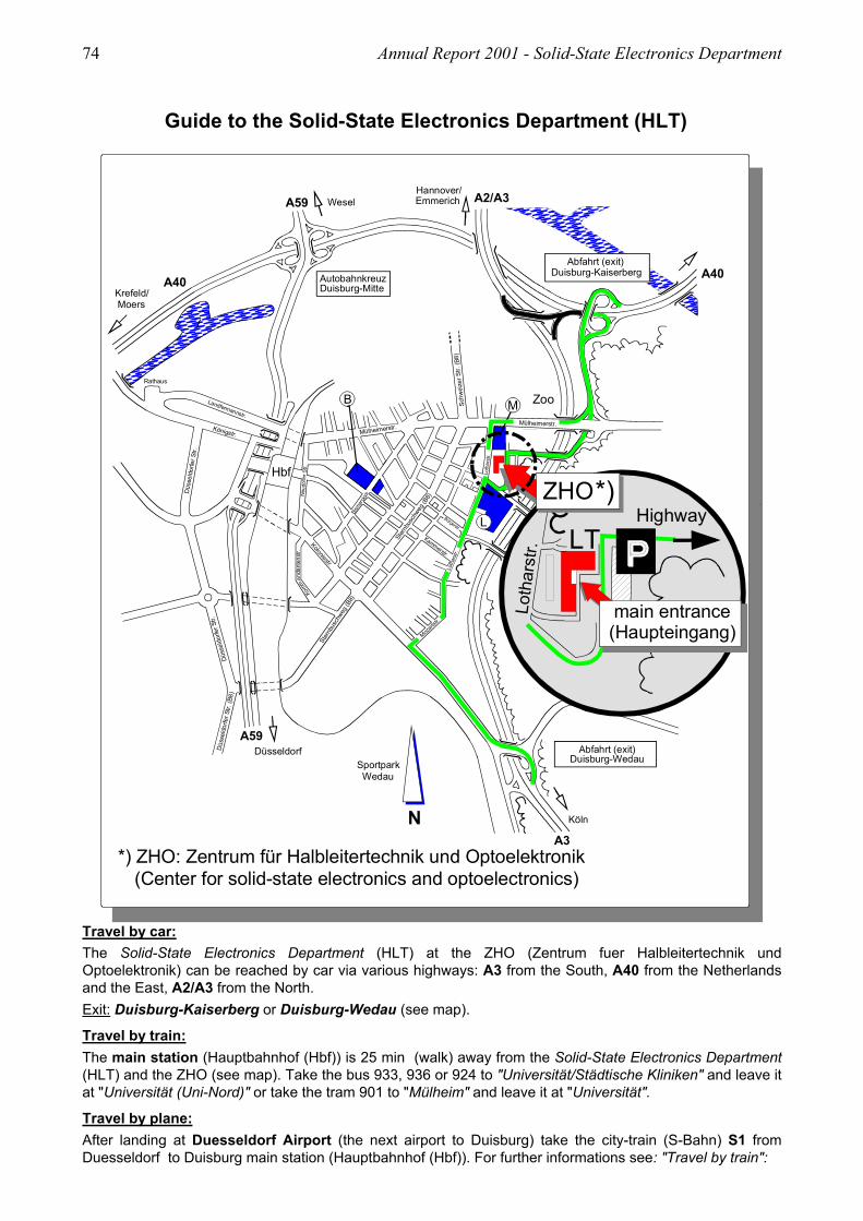
74 Annual Report 2001 - Solid-State Electronics Department
Guide to the Solid-State Electronics Department (HLT)
B M
Hbf
Mülheimerstr.Mülheimerstr.
Landfermannstr.
Königstr.
Neu
dorfe
r Str.
Komm
anda
nten
str.
Koloniestr.
Bism
arck
str.
Ster
nbus
chwe
g (B8
)
Ster
nbus
chweg
(B8)
Schw
eize
r Str.
(B8)
Mozart
str.
Loth
arst
r.
Loth
arst
r,Finkenstr.
Bürgerstr.
Kammerstr.
Zoo
Abfahrt (exit)Duisburg-Kaiserberg
Abfahrt (exit)Duisburg-Wedau
Autobahnkreuz Duisburg-Mitte
A59 Wesel A2/A3Hannover/Emmerich
A40
A3Köln
A59Düsseldorf
A40Krefeld/ Moers
Rathaus
Düs
seld
orfe
r Str.
Düs
seld
orfe
r Str.
Düs
seld
orfe
r Str.
(B8)
Sportpark Wedau
N
*) ZHO: Zentrum für Halbleitertechnik und Optoelektronik(Center for solid-state electronics and optoelectronics)
LLo
thar
str.
(Haupteingang)main entrance
HighwayLT
ZHO*)
Travel by car: The Solid-State Electronics Department (HLT) at the ZHO (Zentrum fuer Halbleitertechnik und Optoelektronik) can be reached by car via various highways: A3 from the South, A40 from the Netherlands and the East, A2/A3 from the North. Exit: Duisburg-Kaiserberg or Duisburg-Wedau (see map).
Travel by train: The main station (Hauptbahnhof (Hbf)) is 25 min (walk) away from the Solid-State Electronics Department (HLT) and the ZHO (see map). Take the bus 933, 936 or 924 to "Universität/Städtische Kliniken" and leave it at "Universität (Uni-Nord)" or take the tram 901 to "Mülheim" and leave it at "Universität".
Travel by plane: After landing at Duesseldorf Airport (the next airport to Duisburg) take the city-train (S-Bahn) S1 from Duesseldorf to Duisburg main station (Hauptbahnhof (Hbf)). For further informations see: "Travel by train":