Embed Size (px)
Citation preview

ESE-2018 PRELIMS TEST SERIESDate: 29thOctober, 2017
ANSWERS
1. (a)
2. (a)
3. (c)
4. (b)
5. (c)
6. (b)
7. (a)
8. (a)
9. (c)
10. (a)
11. (a)
12. (b)
13. (d)
14. (c)
15. (a)
16. (b)
17. (d)
18. (d)
19. (a)
20. (a)
21. (b)
22. (d)
23. (c)
24. (b)
25. (a)
26. (a)
27. (a)
28. (c)
29. (c)
30. (c)
31. (a)
32. (a)
33. (d)
34. (a)
35. (a)
36. (d)
37. (a)
38. (c)
39. (b)
40. (d)
41. (b)
42. (b)
43. (d)
44. (b)
45. (d)
46. (c)
47. (d)
48. (a)
49. (a)
50. (b)
51. (c)
52. (c)
53. (a)
54. (d)
55. (b)
56. (c)
57. (c)
58. (a)
59. (c)
60. (b)
61. (d)
62. (c)
63. (c)
64. (b)
65. (a)
66. (c)
67. (d)
68. (c)
69. (c)
70. (d)
71. (c)
72. (b)
73. (d)
74. (a)
75. (b)
76. (d)
77. (d)
78. (a)
79. (a)
80. (b)
81. (c)
82. (c)
83. (c)
84. (b)
85. (b)
86. (d)
87. (d)
88. (a)
89. (c)
90. (c)
91. (b)
92. (d)
93. (c)
94. (b)
95. (a)
96. (d)
97. (a)
98. (a)
99. (c)
100. (b)
101. (c)
102. (d)
103. (b)
104. (c)
105. (a)
106. (d)
107. (a)
108. (a)
109. (c)
110. (c)
111. (d)
112. (a)
113. (a)
114. (c)
115. (c)
116. (b)
117. (c)
118. (c)
119. (c)
120. (a)
121. (a)
122. (c)
123. (d)
124. (d)
125. (c)
126. (d)
127. (c)
128. (a)
129. (b)
130. (a)
131. (c)
132. (b)
133. (c)
134. (c)
135. (b)
136. (b)
137. (b)
138. (b)
139. (d)
140. (b)
141. (a)
142. (d)
143. (c)
144. (c)
145. (c)
146. (c)
147. (d)
148. (b)
149. (d)
150. (a)

IES M
ASTER
(2) (Test - 06)-29 October 2017
Mobile : E-mail: 8010009955, 9711853908 [email protected], [email protected]. office : Phone : F-126, (Lower Basement), Katwaria Sarai, New Delhi-110016 011-26522064
Web : iesmasterpublications.com, iesmaster.org
1. (a)
Bandgap energy (Eg) of different materials is givenbelow :
Metals : gE 0eV as both the conduction band
and valance band overlapInsulators : Eg > 3 eV
Semiconductors: gE 1 eV
2. (a)
The property of material by which material getspolarized in the direction of external field andremain polarized even after removal of externalfield is called spontaneous polarization. Amongdielectric materials only ferroelectric andpyroelectric materials show spontaneouspolarization; But ferroelectric materials havestrong spontaneous polarization as compared topyroelectric materials.
Material Ferroelectric Para electric
SpontaneousPolarization
Strong Zero Zero
Pyroelectric
Weak
3. (c)
Elements lose (or gain) and share electrons toform ionic and covalent bonds respectively andthese bonds are stable bonds.Conductivity in ionic crystals depends oni) Carrier concentration
ii) Carrier mobility, : This in turn, depends ontemperature and is given by the Arrenhius
expression 0 aexp E kT .
Where Ea = activation energyT = Temperaturek = Boltzmann’s constant
4. (b)The relation between dielectric loss and frequencyis
P f 2 r
rP v 2 fC
so as frequency is doubled, the power loss isdoubled.
5. (c)
There is always dielectric losses occurring in acondenser containing lossy dielectric and thislosses may be accounted as ohmic lossoccurring in resistance R. So, the condensercan be represented as
R C
6. (b)
Steps to find Miller indices :i) Find the intercepts of the plane on the three
crystal axes (OX, OY, OZ) as (pa, qb, rc);where a, b, c are corresponding primitivesand p, q, r be integer.
ii) Write the reciprocal of the number p, q, r as
1 1 1, ,p q r .
iii) Find the LCM of their denominator.iv) Multiply the reciprocals by the LCM, to get
Miller Indices.Herei) Intercepts are (4, 1, 2)
ii) reciprocals : 1 1, 1,4 2
iii) LCM of 4, 1, 2 is 4
iv) Miller indices are 1 14, 1 4, 4 1,4,24 2
7. (a)
Crystal system Unit cell dimension Angle between AxisOrthorhombic a b c 90
Triclinic a b c 90Hexagonal a b c 90 , 120
Cubic a b c 90
8. (a)
Magnetic material
Magnetic susceptibility
DiamagneticParamagneticFerromagneticAntiferromagneticFerrimagnetic
Negative and smallPositive and smallPositive and very largePositive and smallPositive and large
9. (c)
Permanent magnetic materials are difficult todemagnetize. Properties of permanent magneticmaterials :-• High retentivity• High coercivity• High permeability

IES M
ASTER
(Test - 06)-29 October 2017 (3)
Mobile : E-mail: 8010009955, 9711853908 [email protected], [email protected]. office : Phone : F-126, (Lower Basement), Katwaria Sarai, New Delhi-110016 011-26522064
Web : iesmasterpublications.com, iesmaster.org
• Tall and wide Hysteresis loop
• High saturation magnetization
• High Curie temperature
• High hysteresis loss because of large area ofhysteresis loop
10. (a)
• Paramagnetic material are characterized byrandom arrangement of dipole. Due to randomdipole arrangement the value of spontaneousmagnetization is zero.
• When these materials are placed in a magneticfield, they acquire weak magnetization in samedirection of the field.
11. (a)
Hydrogen molecule is a diamagnetic materialwhere as hydrogen atom is paramagnet.
In principle any system that contains atoms,ions or molecules with unpaired spin can becalled a paramagnet. A system with unpairedspins that do not interact with each other aresystem with minimal interaction. Each hydrogenatom has one non-interacting unpaid electron.
12. (b)
Magnetic susceptibility
= Relative permeability – 1
= 5500 – 1 = 5499
13. (d)Total polarization of a polyatomic gas,
P = Pe + Pi + Po
0 eE = 2p
e iNp E
N E N E3KT
0 r 1 E =
2p
e ip
N E3KT
0 r
y
1=
2p
e i
c xm
Np 1N3K T
i.e. y = mx + cThis is an equation of straight line, having slope
m = 2pNp
3K
14. (c)Face centred cubic :
a
r
rr
r
where r = radius of an atomIn face-centred cubic lattice, atoms are locatedat each corner and at the centre of each face ofunit cell.
So, 4.r = a 2
r =a 2
4 =
a2 2
15. (a)
We know that
C
D
| J || J |
9 9
101100 10 10
36
= 1010 36
= 1036 10 1
hence it is a good conductor.
16. (b)
17. (d)Ferromagnetic materials obey Curie - Weisslaw,
m = C
Twhere, C is the curie constant and is calledthe paramagnetic curie temperature.Above the curie-temperature ferromagneticmaterials, behaves l ike paramagneticmaterials.
18. (d)
Half-coefficient of semiconductor materials
RH =1
ne

IES M
ASTER
(4) (Test - 06)-29 October 2017
Mobile : E-mail: 8010009955, 9711853908 [email protected], [email protected]. office : Phone : F-126, (Lower Basement), Katwaria Sarai, New Delhi-110016 011-26522064
Web : iesmasterpublications.com, iesmaster.org
where n is the carrier-concentration,
A
B
RR
=
21B
21A
n 4 10 4 : 1n 1 10
19. (a)Superconductor shows diamagnetism. Hence,it expels magnetic flux from within its volume.A superconductor becomes a normal metalwhen a critical magnetic field is applied.
Superconductor
(T < T )C
BB = 0
H
HC
0 TC T
Normal StateSuperConductingState
20. (a)At equilibrium,
yqE = x zqV .B
Vx =y
z
EB ....(1)
and, Jx = NqVx .....(2)So, Hall coefficient, RH
= y x
z x x
E V 1B J Nq.V Nq
21. (b)
Hall effect occurs when a transverse magneticfield is applied to a conductor carrying current.Due to the current, a longitudinal electric fieldnormally present in the direction of flow ofcurrent.
22. (d)The conductivity at any given temperature(except at absolute zero) is due to bothelectrons and holes, and it is given by
i = i e hn e
=
e h2
ie h
n em m
where
i = conductivity of intrinsic material
e h, = relaxation time for electrons andholes
e hm ,m = mass of electron and holes
e h, = mobility of electron and holes
23. (c)
• The semiconductor in its purest form iscalled intrinsic semiconductor e.g. Si, Ge
• When some impurity is added to theintrinsic semiconductor, i t is calledextrinsic semiconductor.
• N-type semiconductor and P-typesemiconductor are classified on the basisof type of impurity added.
• If impurity is a donor (or Penta valent) e.g.P, Ar, Sb, etc. it is cal led N-typesemiconductor.
• If impurity is a acceptor (or tri valent) e.g.B, Al, Ga etc.
24. (b)
Let x is the displacement of electron and Eis applied electric field across conductor.
F =
2
e 2d xm eEdt
dxdt =
e
eE drift velocitym
As, mobility,
µ =drift velocity
Electric field intensity
=
e
eEm
E
=
e
em
25. (a)For a superconductor, critical field HC varieswith temperature as,
HC =
2
0C
TH 1T
where, H0 is the critical field at absolute zeroand TC is the transition temperatureSo, at T = TC; HC = 0

IES M
ASTER
(Test - 06)-29 October 2017 (5)
Mobile : E-mail: 8010009955, 9711853908 [email protected], [email protected]. office : Phone : F-126, (Lower Basement), Katwaria Sarai, New Delhi-110016 011-26522064
Web : iesmasterpublications.com, iesmaster.org
26. (a)A good electric contact should offer lowresistance to flow of current. This reducesthe voltage drop and also heat generated atcontact points.
27. (a)• Superconductors are used for generating
very strong magnetic field.If a superconductor caries a current I, thendeveloped magnetic field
H =I
2 r
where r is the radius of superconductorwire.
• Magnetic bubble memories are built usingferrites.
28. (c)The temperature below which a normalmaterial behaves as a superconductor, iscalled transition temperature of that material.Experimentally, it is found that transitiontemperature of mercury is 4.12 K.
29. (c)For any intrinsic semiconductor, the intrinsicconcentration is directly proportional to T3/2.As conductivity of the instrinsic semiconductoris directly proportional to intrinsic
concentration. So, 3/2T .
30. (c)For the semiconductor material,
The Hall’s coefficient, Rx =
y
x z
E 1J B ne
As, = ne
So, RH =
1 1
ne
31. (a)
Since, Hall coefficient, RH = 1
ne
Where n is number of charge-carrier per unitvolume; m–3.and e is the charge of electron; coulomb. Sounit of RH : (meter)3 (coulomb)–1
So, option (a)
32. (a)
The current required to flowing through a superconductor of radius ‘r’ to produce a criticalmagnetic field Hc is
Ic = c2 r H
= cd2 H2
=
3
322 102 7 107 2
= 22 Ampere
33. (d)
As, fermi level for P-type semiconductor,
EF = VV e
A
nE KT log
N
where,EV = maximum energy of valence band in eV.
nV = no. of electrons in valence band,NA = concentration of acceptor atoms.
i.e.
Conduction band
Fermi level for P-type semiconductor
Valence band
34. (a)
35. (a)According to the Messener’s ef fect,superconductors expels the magnetic fieldflowing through it.So, relative permeabil i ty is zero forsuperconductor.
36. (d)Transformer oil acts as insulator and coolingmedium for transformer cores and chokes. Itsdielectric strength should be high to work as agood insulator. Flash point and viscosity arealso important parameters for transformer oil.Flash point is the lowest temperature at whichit vaporize. For better temperature stability it

IES M
ASTER
(6) (Test - 06)-29 October 2017
Mobile : E-mail: 8010009955, 9711853908 [email protected], [email protected]. office : Phone : F-126, (Lower Basement), Katwaria Sarai, New Delhi-110016 011-26522064
Web : iesmasterpublications.com, iesmaster.org
should be high. Viscosity is a measure of itsresistance to gradual deformation by stress soits should also be high for transformer oil.
37. (a)Power loss of a dielectric in alternating electric
field 20 0 r
1 E2
So power loss
38. (c)Temperature has no effect upon ionic polarizabilityand electronic polarizability.
39. (b)Sodium is paramagnetic.
40. (d)Ferrites from magnetic would be in form of
MO.Fe2O3 (M = divalent metal)it can be represented as
AB2O4 (A, B = metals)41. (b)
Neel temperature is the transition temperaturebetween anti-ferromagnetism and para-magnetism behaviour of a material.
42. (b)Bohr magneton is the unit of permanent dipolemoment due to spin of electrons in orbit.
1 Bohr magneton = eh
4 m= 9.27 × 10⁻²⁴ ampere.m2
where, h = plank’s constant= 6.62 × 10⁻³⁴ joule sec.
m = mass of electrone = charge of electron
43. (d)
As we know, mean free path, d= v and
31T
44. (b)According to wiedemann – Franz law
=TKThermal conductivity
Electrical conductivity =
22 k .T3 e
where, k = Boltzmann’s constant
e = Electronic charge
T = Temperature
The ratio of thermal conductivity and electricalconductivity is proportional to temperature andthis law holds good above debye temperature.
45. (d)If a super conducting material is placed inmagnetic field (H) it remains superconductorupto a critical field (Hc) above that it turns intonormal state. Similarly it remains superconductorbelow a transition temperature and above thattemperature it converts into normal state.
Magnetic impurities can also contribute towardscritical field.
46. (c)Rochelle’ salt is a piezoelectric crystal, whichis used as piezoelectric transducer.Piezoelectric transducers convert mechanicalmotion to electrical signal.
47. (d)
Diamagnetic material is the only magneticmaterial which has no dipoles.
48. (a)
Vab = ab cd1
d i d iL m
dt dt
= 38 10 5 100 cos t
315 10 5 100 cos t
= 4cos t 7.5cos t volt.
= 11.5cos t volt.
Vcd = cd ab2
d i diL M
dt dt
= 324 10 5 100 cos t 315 10 5 100 cos t
= 12 cos t 7.5cos t
= 22.5cos t volt.
Where 100rad / s.
49. (a)Here, the instantaneous voltage andinstantaneous current are in phase whichindicates that the circuit is in resonance so,the net impedance z = R.
R =m
m
VI
= 75 515
At resonance,
20 =
1LC

IES M
ASTER
(Test - 06)-29 October 2017 (7)
Mobile : E-mail: 8010009955, 9711853908 [email protected], [email protected]. office : Phone : F-126, (Lower Basement), Katwaria Sarai, New Delhi-110016 011-26522064
Web : iesmasterpublications.com, iesmaster.org
L = 20
1C
= 2 6
1
100 400 10
=14
= 0.25 H
50. (b)
Since the current flowing in the loop is ‘i’,
Hence,
3i – 5 = i
2i = 5
i = 2.5A
So, the voltage across the 5 resistor..
VL = 5i
= 5 × 2.5
= 12.5 volt
51. (c)
From the circuit, we can observe that voltageat point ‘b’ is 20V
bV 20 V
Also, Va–10 = Vb
Va = Vb + 10 = 20 + 10 = 30V
i.e. aV 30 V
and, Vb–5 = Vc
VC = 20 – 5 = 15V
CV 15 V
52. (c)Given circuit is,
5
31
3i4A
i(i–i )L
1
Current through 5 resistor, i 4A
Applying KVL is loop (1), we get
3i + (i – iL) – 3iL = 0 i = iL iL = 4A
So, voltage across 3 resistor = 4 × 3 = 12V
53. (a)
R R
B BY
Y
rr
Let RY YB BRV V V V
If all the resistance are present is loadPower, P = 3 VPh·IPh cos
= 3·V·VR
cos 1, resistive
=23V
RIf one of the resistances of the load gets opencircuited,Power P = 2 VPh IPh cos
= 2 V VR
=22V
R% reduction in power
=
P P 3 2100 100
P 3= 33.33%
54. (d)
In a power measurement of 3 unbalancedload,
1 L L
2 L L
W V I cos (30 )W V I cos (30 )
and,
2 1
2 1
W Wtan 3W W
When, = 0 ie. Pf is unity W1 = W2 > 0When, = 60° ie. pf = 0.5 (lag) W1 = 0 but W2 > 0When, = 90° ie. pf is zero W1 = –0.5 Vl ILand W2 = 0.5 VL ILie. W2 = –W1 or, W1 + W2 = 0.
55. (b)A. For RL circuit voltage loads current by an
angle 1 Ltan
RB. For RC circuit voltage lags current by an
angle
1 1tanRC

IES M
ASTER
(8) (Test - 06)-29 October 2017
Mobile : E-mail: 8010009955, 9711853908 [email protected], [email protected]. office : Phone : F-126, (Lower Basement), Katwaria Sarai, New Delhi-110016 011-26522064
Web : iesmasterpublications.com, iesmaster.org
C. For a pure capacitive circuit current leadsvoltage by an angle 2 .
D. For a pure inductive circuit current lags
voltage by an angle 2 .
56. (c)
50V Choke10AHeater
200V, 50Hz
Given : I 10A, VH (drop across heater) = 50VRC ( Resistance of choke) 5Vs = 200V
RH (Resistance of heater) = 50 510
Hence, net resistance of the circuit is,
R = RH + RC = 5 + 5 = 10
HRV (drop across RH) = RH × I = 5× 10 = 50V
CRV = RC × I = 50V
LRV (drop across XL, the inductive reactance
of the choke) = I XL = 10 XL V.
However, the supply voltage being the vectorsum of the drops VR and VL.
V = C HR R LV V jV
(200)2 = 2 2L50 50 V
2LV = 2002 – 1002
VL = 173.21 V
XL =173.21 173.21 17.23
I 10
This gives the impedance of the choke as
Z = 2 2 2 2C LR X 5 (17.32) 18
57. (c)Given voltage source, v = 1+sint
v 2
1
t
we see that, 0 0,i 10v
Here, v = the voltage across the non linearVoltage across the non linear resistor
= v – 1 × i = v – i
i = 10 (v – i)
i = 10 v – 10 i
11i = 10 v
i =10 v11
= 0.91 (1+sint)
58. (a)The circuit shown in question, can be redrawnas,
b
d
2
2
2 2
I
a n c
3
10V
Here, Rbn = Rcn = Rdn =
6 6
6 6 6
= 36 218
Req = [(4) || 5] + 2
= 20 3829 9
Current, =eq
VR
= 10
(38 / 9)
= 90 2.34 A38
59. (c)Given circuit is,
4A +– 2V
5Va
+ –
b1
2
(I–1)
(4–I)
1AI
Current in 2 resistor
= 2 1A2
Applying kVL in loop (i), we get
– 5 + I × 1 = 0 I = 5A
So, current in section a–b,
abΙ = I – 1
= 5 – 1 = 4A

IES M
ASTER
(Test - 06)-29 October 2017 (9)
Mobile : E-mail: 8010009955, 9711853908 [email protected], [email protected]. office : Phone : F-126, (Lower Basement), Katwaria Sarai, New Delhi-110016 011-26522064
Web : iesmasterpublications.com, iesmaster.org
60. (b)Given circuit is,
6V +– 6A 2
1
(I+6)+
I4
–Let current delivered by voltage source = IApplying kVL in loop-1, we get6 – 4I – 2(I + 6) = 0
6 – 4I – 2I – 12 = 0
6I = –6 I = –1A
So, power delivered by voltage source = 6I
= 6 × (–1)
= –6W
Now, voltage across current source
= 2 ( 6)
= 2 × (–1 + 6)
= 10 volt
So, power delivered by current source
= 6 × 10
= 60 W
61. (d)Since,
cos2t = cos²t – sin²t
= 1 – 2sin²t
sin²t = 1 (1 cos2t)2
L[sin²t] = 2 21 1 s2 s s 2
=2 2
21 s 4 s2 s(s 4)
= 21 42 s(s 4)
= 22
s(s 4)
62. (c)Since, capacitive reactance
Xc =1c
= 1
2 fc
ie. capacitive reactance Xc increases if both Cand f decreases.
63. (c)Given circuit is under resonance, so currentwill be maximum,
Irms = rmsVR
= (10 / 2)
100Average power will be dissipated only inresistor.
So, Pavg = 2rms( ) R
=
210 / 2 100
100
=100
2 100= 0.5 W
= 500 mW
64. (b)Since, current will leave the dot in first inductorand enter the dot in second inductor, hence.equivalent inductance will be,
Leq = L1 + L2 – 2M= 6 + 4 – 2 × 2
= 6 H
So, resonance frequency, 0 = eq
1L C
0 =
1163
= 12
= 0.707 rad/sec.
65. (a)
For RTh
2
2 2a
b Rab = (4) 2
=86
= 1.33

IES M
ASTER
(10) (Test - 06)-29 October 2017
Mobile : E-mail: 8010009955, 9711853908 [email protected], [email protected]. office : Phone : F-126, (Lower Basement), Katwaria Sarai, New Delhi-110016 011-26522064
Web : iesmasterpublications.com, iesmaster.org
i.e. RTh = 1.33
For VTh:By transformation theorem, the circuit can beredrawn as,
–
+
20A
2 2a
b
4V
+–
2
I
I =
20 4
4A6
Vab = 2I – 4 = (2 × 4) – 4 = 4V
i.e. VTh = 4V66. (c)
For lattice network, the z-parameters are,
z11 = z22 = 1 2z z2
and z1 = z11 = 2 1z z2
So, z11= z22 =
6 4 5
2
and, z12 = z21 =
6 4 1
2 |z| = z11 z22 – z12 z21
= (5 × 5) – (1 × 1) = 24Then,
h11 =
22
z 24z 5
h21 = 21
22
z 1z 5
67. (d)For T-network,
Z1 Z2
V1 V2
+ +
––
Z2
11 12
21 22
Z ZZ Z
=1 2 3
3 2 3
Z Z ZZ Z Z
=40 R R
R 30 R
Fiven, Z12 = Z21 = 20ie. R = 20So, Z11 = 40+R = 40 20 60
and Z22 = 30 + R = 30 20 50
68. (c)For the given circuit
V1 = (I1 + I2) Za
And, V2 – 2 b 1 2 aI z (I I )z 0
V2 – 2 b 1I z V 0 V1 = V2 – I2 zb
V1 = V2 – I2 × 2 …(1)and V2 = I2 (za + zb) + I1 za
I1 = 2 2 a ba
1 V I z zz
I1 = V2 – 3I2 …(2)For ABCD parameters
1
1
VI
=
2
2
VA BIC D
A BC D
=
1 21 3
69. (c)The frequency at which the voltage across thecapacitor is maximum,
maxcf =
2
21 1 R
2 LC 2Lwhich is below the resonance frequency, f0 =
1
2 LC
The frequency at which the voltage across theinductor is maximum
maxLf =
2 2
1 12 C RLC
2which is above the resonance frequency, f0 =
1
2 LC
70. (d) Quality factor,
Q =resonant frequency
Bandwidth =
0ff
=
6
320 10
100 10 = 200

IES M
ASTER
(Test - 06)-29 October 2017 (11)
Mobile : E-mail: 8010009955, 9711853908 [email protected], [email protected]. office : Phone : F-126, (Lower Basement), Katwaria Sarai, New Delhi-110016 011-26522064
Web : iesmasterpublications.com, iesmaster.org
71. (c)
72. (b)
11 22 12 21
11 22 12 21
11 22 21 12
21 12
Symmetry Reciprocity1. Z parameter Z Z Z Z2. Y parameter Y Y Y Y3. h parameter h h h h
h h 14. ABCD parameter A D AD BC 1
73. (d)
Transmission Parameters Network ‘b’
=1 a 1 a3 2 3 2
=
1 3a 3a A B9 3a 4 C D
For reciprocity, [AD – BC] = 1
9 13a 4 1 3a 3a
29a 12a 4 = 1
a = 1 or 1/3
74. (a)
For z-parameter, we get
V1 = 1 225I 10I ...(1)
and V2 = 1 2200I 200I ...(2)
For the given network,
V2 = 250I ...(3)
From (1) and (3),
V2 = 21
V200I 5050
V2 = 1100I
100I1 = –50I2 [For eqn. (2)]
–2I1 = I2
V1 = 1 225I 10 2I
[For eqn. (1)]
= 45I1
Zin = 1
1
V45
I
75. (b)
For a passive network, the output power cannotbe greater than the input power.
76. (d)
For Z11 and Z21, put I2 = 0, then
Z11 = 11
1
V ZI
Z21 = 21
1
V ZI
For Z12 and Z2, put I1 = 0, then
Z12 = 11
2
V ZI
Z22 = 21 2
2
V Z ZI
Z-parameters are
1 1
1 1 2
Z ZZ Z Z
77. (d)
A
B
CinCin
Cin = in
in
C CC
C C
CAB = in1 5C C
278. (a)
When in series, we have to add the Z-parametersto combine the two, two network.
79. (a)
L-C network has only energy storage element.Power dissipation elements ‘R’ is not there, sothe poles and zeros lie on the imaginary axis.Network function should be determined by zeroinitial condition.
80. (b)
2Ai
6A 1A
4A3A
a

IES M
ASTER
(12) (Test - 06)-29 October 2017
Mobile : E-mail: 8010009955, 9711853908 [email protected], [email protected]. office : Phone : F-126, (Lower Basement), Katwaria Sarai, New Delhi-110016 011-26522064
Web : iesmasterpublications.com, iesmaster.org
Applying KCL at node a, we get
6A 1A 4A 3A 0
i = 2A
81. (c)For obtaining equivalent resistance,we haveto short circuit the independent voltage sourceand open circuit indepdent current source.Therefore the circuit is,
2 2
1
1
RTh
RTh= 2 2 2
= 2 1= 3
82. (c)
Using superposition theorm, current in 10resistor due to 10A current source is
I1 = 1010A20
= 5A
5
5 10 10A
Current in 10 resistor due to 20A currentsource is
5
5 1020A
I2 =
520A20 = 5A
Total current = I1+I2= 5+5 = 10A
83. (c)
From linearity we known that s LV I ratioremains constant.
Now power absourbed is 2.5W, so2L LI R = 2.5W
IL = 0.5AFrom Linearity,
20V200mA = SV
500mAVs = 50V
84. (b)Applying superposition therom, it is knownthat if all current source value are doubled,then node voltages also are doubled.
85. (b)
Power obserbed by RL is,
PL =
2s L
2s L
V R
R R
from the expression, power is maximum whenRs = 0.
86. (d)
Thevenin equivalent of unknown circuit is
RV
RTh
VTh
by voltage division V =
ThTh
RVR R
substituting values from table,
6 =
ThTh
3VR 3
...(1)
8 =
ThTh
8VR 8
...(2)
Solving the equation (1) and (2), we get
RTh = 2 and VTh = 10V
87. (d)
[Y] = 1Z
11 12
21 22
Y YY Y =
22 12
21 1111 22 12 21
Z Z1Z ZZ Z Z Z
=
22 12
21 11
Z Z1Z ZZ
[Where Z = Z111Z22 – Z12Z21]

IES M
ASTER
(Test - 06)-29 October 2017 (13)
Mobile : E-mail: 8010009955, 9711853908 [email protected], [email protected]. office : Phone : F-126, (Lower Basement), Katwaria Sarai, New Delhi-110016 011-26522064
Web : iesmasterpublications.com, iesmaster.org
88. (a)When switch was open, total charge q= 1 1C V
Let after closing the switch; voltage acrossparallel combination is V.
t 0
VC1 C2
As charge will be conserved.
Now, q = eqC .V
ie. 1 1C V = 1 2C C V
V =1 1
1 2
C VC C
89. (c)
Power P = 2rmsi R
Here 2rmsi =
T2
0
1 i t dtT
= 3
2
0
1 3t dt 273
2rmsi R = 270W
R =270 1027
90. (c)
1
1L 1 1 2
di t dV t L M i t i tdt dt
2
1L 2 1 2
di tdV t L i t i t Mdt dt
• Multually induced voltage occurs due toother current .
• Self induced voltage occurs due to selfcurrent.
91. (b)
T0
A
t
f t
T0
A
t
1Af t tT
T0
1
t
2f t u ut t T
= ×
f(t) = 1 2f .ft t
= A t u ut t TT
= A Atu tut t TT T
= A Atu ut t T T t TT T
= A Atu u Aut t T t T t TT T
92. (d)The single voltage source may be consideredto be equivalent to two identical sources inparallel. So option (1) and option (4) areequivalent.Option (4) and option (3) are equivalent sincea connection from the positive terminals of thetwo sources does not affect the networkbecause there would be no current in such aconnection.Note: The single current source may beconsidered to be equivalent to two identicalsources in series.
93. (c)L1 = 5 mH, L2 = 20 mH
L N2
It the number of turns are doubled the newvalue of
1L = 212 L
= 4 5 20 mH
2L = 222 L
= 4 20 80 mH
Total InductanceLeq = L1 + L2 – 2 M
(For negative polarity)
M = 1 2K L L
= 0.5 20 80= 0.5 40= 20
Leq = 20 + 80 – 40= 60 mH
94. (b)
Applying KVL in 1st loop we get
36 = 3120 10 I
I1 = 336 1.8mA
20 10

IES M
ASTER
(14) (Test - 06)-29 October 2017
Mobile : E-mail: 8010009955, 9711853908 [email protected], [email protected]. office : Phone : F-126, (Lower Basement), Katwaria Sarai, New Delhi-110016 011-26522064
Web : iesmasterpublications.com, iesmaster.org
+
–5 k
10 I2
vI2
20 kI1
36V
1
1
Applying KCL at node 1I2 = I1 + 10 I2
I2 = 1I 0.2mA9
Voltage across 5K resister
v = 325 10 10I
= 3 35 10 10 0.2 10= 10 V
95. (a)i = 2 A
Applying KVL, we getVab– 3i +10 = 0
Vab = 3i – 10
= 3 2 10
= –4 V96. (d)
20V
2
i+
–v
Given4i = v2 – 8 ...(1)
Applying KVL we get20 – 2i = v ...(2)
From equation (1) and (2), we get4i = (20 – 2i)2 – 8
4i = 400 + 4i2 – 80i – 8 i = 100 + i2 – 20i – 2 i2 –21i + 98 = 0 (i – 7) (1– 14) = 0 i = 7, 14 A
97. (a)
Irms = T
2
0
1 8t dtT
=31 64 T
T 3
Here T = 1
Irms =643
Average Power loss in 9 resistorPav = 2
rmsI 9
=64 93
= 192 W98. (a)
Electric field is given by :
1 21 22
0 1 0 2
Q Qˆ ˆE r a a4 r r 4 r r
where 1a and 2a are unit vectors along 1r r
and 2r r
.
Here, 1ˆ ˆ ˆr r 0 1 i 0 2 j 0 2 k
ˆ ˆ ˆi 2j 2k
2 2 21r r 1 2 2 3
And, 2ˆ ˆ ˆr r 0 3 i 0 6 j 0 6 k
ˆ ˆ ˆ3i 6 j 6k
2 2 22r r 3 6 6 9
9 6 ˆ ˆ ˆi 2j 2k3 9 10 10E 0,0,0
9 3
6 9 ˆ ˆ ˆ3i 6 j 6k27 10 9 1081 9
3 3ˆ ˆ ˆ ˆ ˆ ˆE 10 i 2j 2k 10 i 2j 2k V m
3ˆ ˆ ˆ ˆ ˆE i i 2 j 2 j 2k 2k 10 V m
ˆ ˆE 4 j k kV m
99. (c)
C1
C2
C3

IES M
ASTER
(Test - 06)-29 October 2017 (15)
Mobile : E-mail: 8010009955, 9711853908 [email protected], [email protected]. office : Phone : F-126, (Lower Basement), Katwaria Sarai, New Delhi-110016 011-26522064
Web : iesmasterpublications.com, iesmaster.org
Here, C2 = 0 03 A 3 Ad d22
C3 = 0 04 A 4 Ad d22
C1 = 0 02 A 4 Ad d2
C2 and C3 are in parallel : 2 3C C C
C = 07 Ad
Now, C and C1 are in series.
Ceq =
2
001
10
A28ACC 28d
AC C 11 d11d
100. (b)
Magnetic flux is given by B A weber
2WeberB
mA.
Magnetic field intensity unit is Ampere/m.
101. (c)
Ampere law states that line integral oftangential component of H around a closedpath is the same as net current I enclosed bythe path.
encH dl I
Applying Stokes Theorem:
Ienc =
s
H dl H dS
Ienc =
S
J dS
H =
J (in point or differential form)
102. (d)
Gauss Law is given by :
eneD ds Q
VB p
Magnetic field lines always exist in closed pathsand magnetic monopole does not exists.
E 0Electric field lines never exist in closed path
Hence,
E 0
103. (b)
Magnetic monopoles does not exist and hencemagnetic field lines are always closed. So, ithas no sinks or sources.
S
B ds = or
B 0
Hence,
B is solenoidal but it is non-
conservative as
H 0.
104. (c)
×
M N
H2H1
Here, = 30°
and H1 = 2I 5H
2 a 2
H1 is due to 10 A at M and H2 is due to 10Aat N.
H1 cos and H2 cos will cancel each other..
Net field intensity = H1 2sin H sin
= 2H1 sin 30°
=
5 122 2
H =
5 Am2 .
IES M
ASTER
(16) (Test - 06)-29 October 2017
Mobile : E-mail: 8010009955, 9711853908 [email protected], [email protected]. office : Phone : F-126, (Lower Basement), Katwaria Sarai, New Delhi-110016 011-26522064
Web : iesmasterpublications.com, iesmaster.org
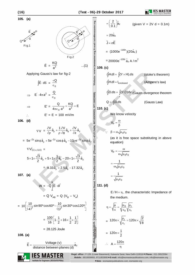
105. (a)
P
Qa
Fig.2
Fig.1
'EP
Qa
E
E = 2
KQa
...(1)
Applying Gauss’s law for fig-2
E ds =
0
Q
' 2E 4 a = 0
Q
E' = 2 2
0
Q KQ E4 a a
E' = E = 100 mV/m
106. (d)
V =
zV 1 V Vˆ ˆ ˆa a a
z
= 2z 2z 2z
zˆ ˆ ˆ5e sin a 5e cos a 10 e sin a
2, 3,0V =
z3 1 3ˆ ˆ ˆ5 1 a 5 1 a 20 1 a
2 2 2
= zˆ ˆ ˆ4.33a 2.5a 17.32a
107. (a)
W = B
A
Q E dl
= Q VAB = Q (VB – VA)
=
2 210 10sin90ºcos60º sin30ºcos120º104 1
= 100 1 1 11 1616 2 2 2
= 28.125 Joule
108. (a)
zVoltage (v)E a
distance between planes (d)
z2 a
0.1
(given V = 2V d = 0.1m)
z20a
J E
= 100rz(1000e )(20a )
= 100r 2z20000e a A / m
109. (c)
H.dl ( H).ds (stoke’s theorem)
enclosedH.dl I (Ampere’s law)
v
D.ds ( .D)dv (Gauss divergence theorem
Q D.ds (Gauss Law)
110. (c)We know velocity
PV
0 0
(as it is free space substituting in aboveequation)
P0 0
V
0 0
1
0 0
1
111. (d)
E / H , the characteristic Impedance ofthe medium.
0 r
0 r
= r
r
2120 1208
= 11202
120A

IES M
ASTER
(Test - 06)-29 October 2017 (17)
Mobile : E-mail: 8010009955, 9711853908 [email protected], [email protected]. office : Phone : F-126, (Lower Basement), Katwaria Sarai, New Delhi-110016 011-26522064
Web : iesmasterpublications.com, iesmaster.org
120 2120 1/ 2
A 2
PV
here 610 Pr r
1 CV
=8 83 10 3 10
42 8
6
810 0.044 0.042
33 10
112. (a)
One may arrive at the correct choice bycomparing the two sides dimensionally.
Since 1 has the dimension of velocity
squared the pertinent choice is:
2 2y y
2 2
E E1
t x
113. (a)The electromagnetic wave equation is given by
22
2E EE 0t t
114. (c)
For free space and are each zero
hence 1 and 2 are false
hence statements 3 and 4 are correct
H J, D
115. (c)
given refractive index ( ) 1.5
frequency = 1410 HZ
Velocity of light in vacuum 8o(C ) 3 10
Velocity of light in glass = C
Refractive index oC( )C
83 101.5C
83 10C1.5
82 10
We know Cf
8
142 1010
62 10
2 m
116. (b)
f(x) V t)0- forward
represents a wave motion in forward direction
f(x) V t)0+ reverse
represents a wave motion in reverse direction
117. (c)dvEdr
given 5
0
6rV
, r 1m
5
0
d 6rEdr
4
0
30r
We also know 20
1 qE4 r
(by Coloumb’s law)
equating both
4
20 0
30r 1 q4 r
6q 30r 4
6q 120 r ( r 1)
q 120 coloumbs
118. (c)
given j /2 jstE (0.5x ye )e
x| E | 0.5

IES M
ASTER
(18) (Test - 06)-29 October 2017
Mobile : E-mail: 8010009955, 9711853908 [email protected], [email protected]. office : Phone : F-126, (Lower Basement), Katwaria Sarai, New Delhi-110016 011-26522064
Web : iesmasterpublications.com, iesmaster.org
2 2y| E | cos / 2 sin / 2 =1
So, x y| E | | E |
and phase = 90°hence it is elliptically polarised wave
119. (c)
For a uniform plane wave
E and H must be in a plane
But both are perpendicular to each other.
120. (a)
• Intrinsic impedance, =
j
j
• For free space, 0 ,
=
0 r 0
0 r 0
jj
r r1, 1
• For conducting medium, ; so,
=
j 45
• For perfect dielectric; 0 ,
=
jj
121. (a)
1.Kirchoff’s current law : Rate of flow of chargeentering at a node is equal to rate of flow ofcharge leaving the node.
2.Ampere’s Law :
H.d Il
3.Faraday’s Law :
dd BAEdt dt
4.Gauss’ Law : D.ds q
122. (c)
As the wave is propagating in Y-direction. Sothe component of electric field will be either inx-direction or in z-direction but never in Y-direction.
123. (d)
When a charged particle is moving itexperiences force due to both magnetic andelectric field.
124. (d)Number of revolutions = 1800/60
= 30 r.p.s
t =1 sec
30
e = t
=425 10
1/ 30
0.23 V
125. (c)
Since, there is no electric field inside theconductor, hence there will be no tangentialcomponent at the surface of conductor. Onlynormal component of electric field will be there.Hence electric lines of force will be alwaysperpendicular to the surface of conductor.
126. (d)As A and B are at the same potential, thework done will be zero.
127. (c)
a
Since charge density = 0
According to Gauss’s Law, D.ds Q
For r < a
2D.4 r = 30
4 r3
D = 0r3
For r a
128. (a)
For a quarter wave
20
inL
ZZ
Z
20 in LZ Z Z
0 in LZ Z Z

IES M
ASTER
(Test - 06)-29 October 2017 (19)
Mobile : E-mail: 8010009955, 9711853908 [email protected], [email protected]. office : Phone : F-126, (Lower Basement), Katwaria Sarai, New Delhi-110016 011-26522064
Web : iesmasterpublications.com, iesmaster.org
given LZ 200
inZ 50
0Z 200 50
10000
0Z 100
129. (b)
given LZ (75 j40)
0Z 75
f 6MHz
as LZ is capacitive in order to havecancelling effect an inductance should beconnected at load so that load matchingtakes place.
130. (a)
We know reflection co-efficient
r 2 1
i 2 1
EE
and 2r
1120
[ r 1 for non-magnetic material]
112016
1204
30
1 120 for free space
30 120150
90150
3
5
131. (c)
Transmission of power to a load over atransmission line achieves optimum valuewhen SWR becomes 1 : 1
This is possible when L 0Z Z
where no reflected wave exists and reflectionco-efficient is zero.
Voltage is uniform along the line
max min| V | | V |
1 0SWR1 0
= 1 : 1
132. (b)
Given 8PV 4 10 m / s
8Zf 10 H
We know PVf
8
84 10
10
4m
length of line l 2m
Since the length of the line is half the wavelength therefore in lZ Z .
133. (c)
We know that
0R j LZG j C
with 0Z as pure resistance we have
L 0 , C 0 , 0RZG
Loss less line
R G 0
0LZC
Distortion less line :
R L ,G C
0LZC
hence it is not lossless line and notdistortionless line
134. (c)
We know reflection co-efficient

IES M
ASTER
(20) (Test - 06)-29 October 2017
Mobile : E-mail: 8010009955, 9711853908 [email protected], [email protected]. office : Phone : F-126, (Lower Basement), Katwaria Sarai, New Delhi-110016 011-26522064
Web : iesmasterpublications.com, iesmaster.org
L 0
L 0
Z ZZ Z
j60 60j60 60
| | =2 2
2 2
60 60
60 60
= 1
VSWR = 1 | |1 | |
= 1 11 1
10
135. (b)
for 2
line
in LZ Z 200
for line4
20
inC
ZZ
Z
2(100)50
100 10050
200
/ 2 line and / 4 line are parallel
in200 200Z 100200 200
for / 8 line, in 0| Z | Z 100
136. (b)
If a change of polarisation direction is required,a twist section may be used extending overtwo or more wavelengths.
Tapers are used to couple waveguides ofdifferent dimensions.
Bends & corners are used to change direction.
137. (b)
Average power is given by d radave 2
G PP
4 r
Here, d 10 dG 10dB 10log G
dG 10
3radP 20 10 w and 3r 10 m
3
ave 610 20 10P
4 10
=
1 W20
138. (b)
Horn antenna, an example of an apertureantenna is a tapered section of a waveguideproviding a transection between a waveguideand the surroundings. It finds its applicationin aircraft.
Parabolic dish Reflector reflects EM waves byconducting sheet. Wired antennas are led bytransmission lines.
139. (d)
The wave is propagating in +z direction. Theexpression of electric field for TM mode isgiven by :
i zZ 0
m x n yE E sin sin ea b
comparing with
i zZE 30sin 50 x sin 60 y e
i zsin 60 y e
m 50a
2m 50a 50 8 10 4
n 60b
2n 60 5 10 3
Mode is 43TM
140. (b)
A waveguide behaves as a high pass filter.There is heavy attenuation for frequenciesbelow cut-off although the waveguide itself isvirtually lossless. Such attenuation is due toreflection at the mouth of the guide and sometake place in evanescent modes.

IES M
ASTER
(Test - 06)-29 October 2017 (21)
Mobile : E-mail: 8010009955, 9711853908 [email protected], [email protected]. office : Phone : F-126, (Lower Basement), Katwaria Sarai, New Delhi-110016 011-26522064
Web : iesmasterpublications.com, iesmaster.org
141. (a)
The wavelength of the wave propagating in awaveguide is given by
2m12a
where Free space wavelength.
Hence is always greater than A.
142. (d)
Phase velocity is the velocity with which thewavechanges phase at a plan foundary andnot the velocity with which it travels along theboundary this apparent velocity which is greaterthan velocity of light in space is called phasevelocity.
143. (c)
A parasitic element shorter than the drivenone or radiator tends to increase radiation inits own direction and behaves as convergentconvex lense which is called a Director.
Radiator
Director
Reflector
A parasitic element longer than the driven oneand which reduces signal strength in its owndirection and increases in opposite directionis called a reflector.
144. (c)
TEM (Transverse Electromagnetic Mode) doesnot have any cut-off frequency and hence itwill be supported at any frequency.
Cut-off frequency is given lay: 0 = m c
nd (formode m)
145. (c)
A waveguide may consist of one or moreconductors, or no conductors at all and willsupport waveguide modes.
146. (c)
For a Transverse magnetic wave propagatingin a waveguide, the electric field component
along the wave propagation is given by:
Ez =
z0
m x n yE sin sin ea b
For m = 0, n 0 , Ez = 0
For n = 0, m 0 , Ez = 0
TM01 and TM10 will not exist and TEM modecannot propagate in a rectangular waveguide.
Only TM11 can propagate.
147. (d)
Loop Antenna consists of a wire with one ormore turns. They are also called wire Antennasand used in Buildings, ships, Automobiles,etc.
Horn Antenna is an example of ApertureAntenna is a tapered section of a wave guide.It is used in Aircraft as it can be convenientlyflush mounted.
Parabolic dish reflector reflects EM wave by aconducting sheet. It is used in communication,Radar & Astronomy. Yagi Uda Array is usedfor short wave transmissions by RadioAmateurs.
148. (b)At absolute temperature, intrinsic semi-conductor behaves like on insulator as thereis no free electrons available.
149. (d)In intrinsic semiconductor, the total electricalconductivity.
e h e hne ne
Although the number of electrons inconduction band and holes in valence bandare equal in intrinsic semiconductor, theconductivity due to electrons is more thanthe conductivity due to holes. Because themobility of electrons is higher than that ofholes.
150. (a)
Alloying elements always increases theresistivity of the metal to which they are added.One reason behind this is, the atomic size ofparent atom and alloying element, are differentwhich leads to the variation in the latticeparameter and thus, the electron scatteringoccurs.