Embed Size (px)
Citation preview
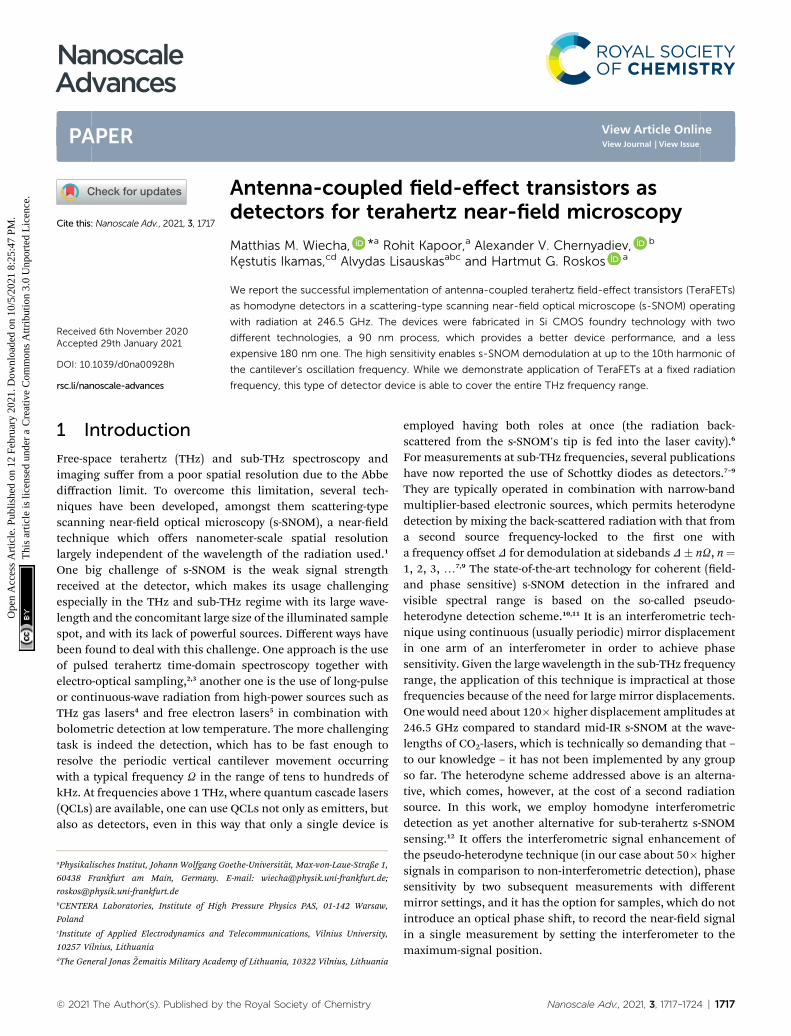
NanoscaleAdvances
PAPER
Ope
n A
cces
s A
rtic
le. P
ublis
hed
on 1
2 Fe
brua
ry 2
021.
Dow
nloa
ded
on 1
0/5/
2021
8:2
5:47
PM
. T
his
artic
le is
lice
nsed
und
er a
Cre
ativ
e C
omm
ons
Attr
ibut
ion
3.0
Unp
orte
d L
icen
ce.
View Article OnlineView Journal | View Issue
Antenna-coupled
aPhysikalisches Institut, Johann Wolfgang Go
60438 Frankfurt am Main, Germany.
[email protected] Laboratories, Institute of High
PolandcInstitute of Applied Electrodynamics and
10257 Vilnius, LithuaniadThe General Jonas Zemaitis Military Academ
Cite this: Nanoscale Adv., 2021, 3, 1717
Received 6th November 2020Accepted 29th January 2021
DOI: 10.1039/d0na00928h
rsc.li/nanoscale-advances
© 2021 The Author(s). Published by
field-effect transistors asdetectors for terahertz near-field microscopy
Matthias M. Wiecha, *a Rohit Kapoor,a Alexander V. Chernyadiev, b
Kestutis Ikamas,cd Alvydas Lisauskasabc and Hartmut G. Roskos a
We report the successful implementation of antenna-coupled terahertz field-effect transistors (TeraFETs)
as homodyne detectors in a scattering-type scanning near-field optical microscope (s-SNOM) operating
with radiation at 246.5 GHz. The devices were fabricated in Si CMOS foundry technology with two
different technologies, a 90 nm process, which provides a better device performance, and a less
expensive 180 nm one. The high sensitivity enables s-SNOM demodulation at up to the 10th harmonic of
the cantilever's oscillation frequency. While we demonstrate application of TeraFETs at a fixed radiation
frequency, this type of detector device is able to cover the entire THz frequency range.
1 Introduction
Free-space terahertz (THz) and sub-THz spectroscopy andimaging suffer from a poor spatial resolution due to the Abbediffraction limit. To overcome this limitation, several tech-niques have been developed, amongst them scattering-typescanning near-eld optical microscopy (s-SNOM), a near-eldtechnique which offers nanometer-scale spatial resolutionlargely independent of the wavelength of the radiation used.1
One big challenge of s-SNOM is the weak signal strengthreceived at the detector, which makes its usage challengingespecially in the THz and sub-THz regime with its large wave-length and the concomitant large size of the illuminated samplespot, and with its lack of powerful sources. Different ways havebeen found to deal with this challenge. One approach is the useof pulsed terahertz time-domain spectroscopy together withelectro-optical sampling,2,3 another one is the use of long-pulseor continuous-wave radiation from high-power sources such asTHz gas lasers4 and free electron lasers5 in combination withbolometric detection at low temperature. The more challengingtask is indeed the detection, which has to be fast enough toresolve the periodic vertical cantilever movement occurringwith a typical frequency U in the range of tens to hundreds ofkHz. At frequencies above 1 THz, where quantum cascade lasers(QCLs) are available, one can use QCLs not only as emitters, butalso as detectors, even in this way that only a single device is
ethe-Universitat, Max-von-Laue-Straße 1,
E-mail: [email protected];
Pressure Physics PAS, 01-142 Warsaw,
Telecommunications, Vilnius University,
y of Lithuania, 10322 Vilnius, Lithuania
the Royal Society of Chemistry
employed having both roles at once (the radiation back-scattered from the s-SNOM's tip is fed into the laser cavity).6
For measurements at sub-THz frequencies, several publicationshave now reported the use of Schottky diodes as detectors.7–9
They are typically operated in combination with narrow-bandmultiplier-based electronic sources, which permits heterodynedetection by mixing the back-scattered radiation with that froma second source frequency-locked to the rst one witha frequency offset D for demodulation at sidebands D� nU, n¼1, 2, 3, .7,9 The state-of-the-art technology for coherent (eld-and phase sensitive) s-SNOM detection in the infrared andvisible spectral range is based on the so-called pseudo-heterodyne detection scheme.10,11 It is an interferometric tech-nique using continuous (usually periodic) mirror displacementin one arm of an interferometer in order to achieve phasesensitivity. Given the large wavelength in the sub-THz frequencyrange, the application of this technique is impractical at thosefrequencies because of the need for large mirror displacements.One would need about 120� higher displacement amplitudes at246.5 GHz compared to standard mid-IR s-SNOM at the wave-lengths of CO2-lasers, which is technically so demanding that –to our knowledge – it has not been implemented by any groupso far. The heterodyne scheme addressed above is an alterna-tive, which comes, however, at the cost of a second radiationsource. In this work, we employ homodyne interferometricdetection as yet another alternative for sub-terahertz s-SNOMsensing.12 It offers the interferometric signal enhancement ofthe pseudo-heterodyne technique (in our case about 50� highersignals in comparison to non-interferometric detection), phasesensitivity by two subsequent measurements with differentmirror settings, and it has the option for samples, which do notintroduce an optical phase shi, to record the near-eld signalin a single measurement by setting the interferometer to themaximum-signal position.
Nanoscale Adv., 2021, 3, 1717–1724 | 1717
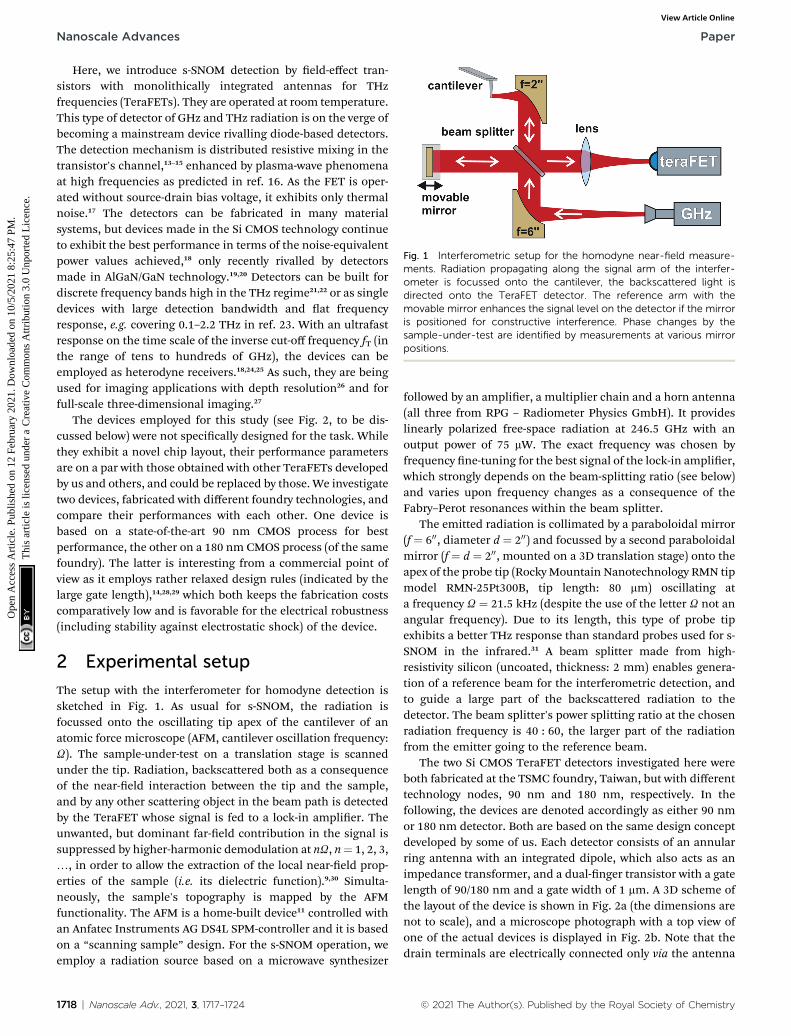
Fig. 1 Interferometric setup for the homodyne near-field measure-ments. Radiation propagating along the signal arm of the interfer-ometer is focussed onto the cantilever, the backscattered light isdirected onto the TeraFET detector. The reference arm with themovable mirror enhances the signal level on the detector if the mirroris positioned for constructive interference. Phase changes by thesample-under-test are identified by measurements at various mirrorpositions.
Nanoscale Advances Paper
Ope
n A
cces
s A
rtic
le. P
ublis
hed
on 1
2 Fe
brua
ry 2
021.
Dow
nloa
ded
on 1
0/5/
2021
8:2
5:47
PM
. T
his
artic
le is
lice
nsed
und
er a
Cre
ativ
e C
omm
ons
Attr
ibut
ion
3.0
Unp
orte
d L
icen
ce.
View Article Online
Here, we introduce s-SNOM detection by eld-effect tran-sistors with monolithically integrated antennas for THzfrequencies (TeraFETs). They are operated at room temperature.This type of detector of GHz and THz radiation is on the verge ofbecoming a mainstream device rivalling diode-based detectors.The detection mechanism is distributed resistive mixing in thetransistor's channel,13–15 enhanced by plasma-wave phenomenaat high frequencies as predicted in ref. 16. As the FET is oper-ated without source-drain bias voltage, it exhibits only thermalnoise.17 The detectors can be fabricated in many materialsystems, but devices made in the Si CMOS technology continueto exhibit the best performance in terms of the noise-equivalentpower values achieved,18 only recently rivalled by detectorsmade in AlGaN/GaN technology.19,20 Detectors can be built fordiscrete frequency bands high in the THz regime21,22 or as singledevices with large detection bandwidth and at frequencyresponse, e.g. covering 0.1–2.2 THz in ref. 23. With an ultrafastresponse on the time scale of the inverse cut-off frequency fT (inthe range of tens to hundreds of GHz), the devices can beemployed as heterodyne receivers.18,24,25 As such, they are beingused for imaging applications with depth resolution26 and forfull-scale three-dimensional imaging.27
The devices employed for this study (see Fig. 2, to be dis-cussed below) were not specically designed for the task. Whilethey exhibit a novel chip layout, their performance parametersare on a par with those obtained with other TeraFETs developedby us and others, and could be replaced by those. We investigatetwo devices, fabricated with different foundry technologies, andcompare their performances with each other. One device isbased on a state-of-the-art 90 nm CMOS process for bestperformance, the other on a 180 nm CMOS process (of the samefoundry). The latter is interesting from a commercial point ofview as it employs rather relaxed design rules (indicated by thelarge gate length),14,28,29 which both keeps the fabrication costscomparatively low and is favorable for the electrical robustness(including stability against electrostatic shock) of the device.
2 Experimental setup
The setup with the interferometer for homodyne detection issketched in Fig. 1. As usual for s-SNOM, the radiation isfocussed onto the oscillating tip apex of the cantilever of anatomic force microscope (AFM, cantilever oscillation frequency:U). The sample-under-test on a translation stage is scannedunder the tip. Radiation, backscattered both as a consequenceof the near-eld interaction between the tip and the sample,and by any other scattering object in the beam path is detectedby the TeraFET whose signal is fed to a lock-in amplier. Theunwanted, but dominant far-eld contribution in the signal issuppressed by higher-harmonic demodulation at nU, n¼ 1, 2, 3,., in order to allow the extraction of the local near-eld prop-erties of the sample (i.e. its dielectric function).9,30 Simulta-neously, the sample's topography is mapped by the AFMfunctionality. The AFM is a home-built device11 controlled withan Anfatec Instruments AG DS4L SPM-controller and it is basedon a “scanning sample” design. For the s-SNOM operation, weemploy a radiation source based on a microwave synthesizer
1718 | Nanoscale Adv., 2021, 3, 1717–1724
followed by an amplier, a multiplier chain and a horn antenna(all three from RPG – Radiometer Physics GmbH). It provideslinearly polarized free-space radiation at 246.5 GHz with anoutput power of 75 mW. The exact frequency was chosen byfrequency ne-tuning for the best signal of the lock-in amplier,which strongly depends on the beam-splitting ratio (see below)and varies upon frequency changes as a consequence of theFabry–Perot resonances within the beam splitter.
The emitted radiation is collimated by a paraboloidal mirror(f ¼ 600, diameter d ¼ 200) and focussed by a second paraboloidalmirror (f ¼ d ¼ 200, mounted on a 3D translation stage) onto theapex of the probe tip (RockyMountain Nanotechnology RMN tipmodel RMN-25Pt300B, tip length: 80 mm) oscillating ata frequency U ¼ 21.5 kHz (despite the use of the letter U not anangular frequency). Due to its length, this type of probe tipexhibits a better THz response than standard probes used for s-SNOM in the infrared.31 A beam splitter made from high-resistivity silicon (uncoated, thickness: 2 mm) enables genera-tion of a reference beam for the interferometric detection, andto guide a large part of the backscattered radiation to thedetector. The beam splitter's power splitting ratio at the chosenradiation frequency is 40 : 60, the larger part of the radiationfrom the emitter going to the reference beam.
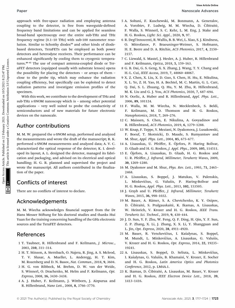
The two Si CMOS TeraFET detectors investigated here wereboth fabricated at the TSMC foundry, Taiwan, but with differenttechnology nodes, 90 nm and 180 nm, respectively. In thefollowing, the devices are denoted accordingly as either 90 nmor 180 nm detector. Both are based on the same design conceptdeveloped by some of us. Each detector consists of an annularring antenna with an integrated dipole, which also acts as animpedance transformer, and a dual-nger transistor with a gatelength of 90/180 nm and a gate width of 1 mm. A 3D scheme ofthe layout of the device is shown in Fig. 2a (the dimensions arenot to scale), and a microscope photograph with a top view ofone of the actual devices is displayed in Fig. 2b. Note that thedrain terminals are electrically connected only via the antenna
© 2021 The Author(s). Published by the Royal Society of Chemistry

Fig. 2 (a) Schematic and (b) real image of the Si CMOS TeraFETdetectors. The dimensions of the antenna metallization (yellow) and ofthe substrate lens (violet) in (a) are not to scale in order bring out thetransistor structure in a clear manner. The annular antenna is thebrighter brown structure in (b), while the dark brown area around itconsists of metal patches which have no antenna functionality at thetarget frequency range; they had to be placed into the detector designin order to obey the design rules of the foundry which demanda certain metal coverage in order to prevent the build-up of excessivemechanical stress.
Fig. 3 (a) Voltage responsivity and (b) noise-equivalent power (NEP) ofthe detector devices. The vertical dotted lines indicate the radiationfrequency of 246.5 GHz.
Paper Nanoscale Advances
Ope
n A
cces
s A
rtic
le. P
ublis
hed
on 1
2 Fe
brua
ry 2
021.
Dow
nloa
ded
on 1
0/5/
2021
8:2
5:47
PM
. T
his
artic
le is
lice
nsed
und
er a
Cre
ativ
e C
omm
ons
Attr
ibut
ion
3.0
Unp
orte
d L
icen
ce.
View Article Online
metallization. Unlike annular ring microstrip antennas or otherpatch antennas,28 the design is based on a ground-plane-freeapproach in order to enable in-coupling of the THz radiationfrom the substrate side. This allows us to easily apply a hyper-hemispherical substrate lens made from high-resistivity single-crystalline silicon (diameter: 12 mm) as schematically shown inFig. 2a. The backside in-coupling comes at the penalty ofmoderate free-carrier-induced absorption losses of the THzradiation in the 280 mm-thick silicon substrates of the detectorchips, which are lightly p-doped (specic resistance as speciedby the foundry: 10 U cm, which corresponds to a carrier densityof 1.25 � 1015 cm�3). The absorption losses lead to a powerattenuation of the THz radiation by about 26%.
A detailed performance characterization of a 90 nm device32
is found in ref. 33. The red curve in Fig. 3 displays the voltageresponsivity and the noise-equivalent power (NEP) of thepresent detector. The responsivity peaks at a value of 408 VW�1,while the best NEP value is 21 pW Hz�1/2. These optimal valuesare reached at 250 GHz, near the operation frequency of ourradiation source, where the responsivity is 402 V W�1 and theNEP remains at 21 pW Hz�1/2. The 180 nm detector exhibits
© 2021 The Author(s). Published by the Royal Society of Chemistry
a responsivity of 380 V W�1 and a noise-equivalent power of27 pW Hz�1/2 at 225 GHz, the frequency of best performance,with the corresponding values at the operation frequency of thes-SNOM being 308 VW�1 and 32 pWHz�1/2, respectively, see theblack curve in Fig. 3. In both cases, the gate bias voltage was0.55 V, and – as usual for TeraFETs – no source-drain biasvoltage was applied in order to operate at the best noiseperformance.
During the s-SNOM measurements, the rectied outputsignal of the TeraFET is fed into a lock-in amplier (ZurichInstruments MFLI) for higher-harmonic demodulation. In theexperiments described in the following, the position of themirror in the reference arm remained xed at a position ofconstructive beam interference, found by maximizing the 1U s-SNOM signal at the beginning of themeasurement on ametallicregion of the respective sample-under-test.
3 Results and discussion
Fig. 4 and 5 display so-called approach curves at variousdemodulation frequencies for the two detectors. The curveswere recorded with a Au-on-Si sample bymeasuring the s-SNOMsignal as a function of the distance between tip apex and sampleupon retraction of the tip. All data represent single distancescans and were measured with the same integration timeconstant tc ¼ 100 ms of the lock-in amplier. The slow decay ofthe 1U s-SNOM signal with increasing distance indicates thatthere are strong background contributions present at the
Nanoscale Adv., 2021, 3, 1717–1724 | 1719

Fig. 4 Approach curves recorded with a Au film as sample-under-testwith the 180 nm detector. The curves were recorded at differentdemodulation frequencies: at the fundamental tip oscillationfrequency 1U and at different harmonics n from 2U to 7U. The dottedline at 100 nm serves as a guide to the eye to facilitate visual distinctionof the signal rise upon approach of null distance.
Fig. 5 Approach curves at different harmonics from 1U up to 10Umeasured with the 90 nm detector. The dotted line is placed ata distance of 100 nm, cf. Fig. 4.
Table 1 SNR values obtained for radiation back-scattered froma freely oscillating tip and recorded at the fundamental frequency 1U(“1U (free)”) in comparison with the SNR values found in s-SNOMmeasurements with demodulation at nU for a tip in interaction witha Au surface (“nU (s-SNOM)”). Values are for a time constant of tc ¼ 1 sof the MFLI lock-in amplifier for both detectors. In addition, the lowerline presents values for tc ¼ 100 ms for the 90 nm detector
SNR1U(free)
1U(s-SNOM)
2U(s-SNOM)
3U(s-SNOM)
4U(s-SNOM)
180 nm (1 s) 53 108 39 10 1290 nm (1 s) 388 387 49 49 3990 nm (100 ms) 58 78 18 10 8
5U(s-SNOM)
6U(s-SNOM)
7U(s-SNOM)
8U(s-SNOM)
9U(s-SNOM)
10U(s-SNOM)
— — — — — —27 15 12 8 8 54.6 4.0 2.9 2.1 1.7 1.4
Nanoscale Advances Paper
Ope
n A
cces
s A
rtic
le. P
ublis
hed
on 1
2 Fe
brua
ry 2
021.
Dow
nloa
ded
on 1
0/5/
2021
8:2
5:47
PM
. T
his
artic
le is
lice
nsed
und
er a
Cre
ativ
e C
omm
ons
Attr
ibut
ion
3.0
Unp
orte
d L
icen
ce.
View Article Online
fundamental tip oscillation frequency, whereas the signals athigher harmonics (n $ 2) continue to decay more rapidly withrising distance as the order number n increases, revealingincreasingly stronger localization of the respective electric eldsat the apex region of the tip. In addition, one clearly notices theincrease of the noise level with the order of the harmonicswhich is a consequence of the decrease of the signal-to-noiseratio (SNR) with rising value of n. The high sensitivity of the90 nm detector allows to obtain useful signals up to n ¼ 10.
Table 1 species SNR values obtained with both devices fromthese and other approach-curve measurements. The table listsvalues for a time constant of the lock-in amplier of tc ¼ 1 s; forthe 90 nm device, we also present SNR values for tc ¼ 100 ms,because it is common in the literature to provide noise-relatedperformance data such as SNR and NEP values for this inte-gration time. The rst value in the table is for a freely oscillatingtip away from a sample surface, the signal being that back-scattered from the tip upon standard illumination alignmentand recorded at 1U. The other values are for the tip interactingwith the Au surface (same beam alignment), recorded at thevarious demodulation frequencies 1U to 10U. The 90 nm Ter-aFET exhibits a 3–5� better SNR than the 180 nm device, andreaches a performance level which is comparable to (or evenbetter than) that reached with Schottky diodes as detectors, forwhich one nds SNR values > 10 for demodulation at 2U in
1720 | Nanoscale Adv., 2021, 3, 1717–1724 © 2021 The Author(s). Published by the Royal Society of Chemistry

Fig. 7 Large-area images at a Au–Si edgewith a dirt particle sticking tothe edge (length of scale bar in (a): 2 mm). Au is on the left side, Si on theright. (a) Topography, (b–d) 1U to 3U s-SNOM maps taken with the180 nm TeraFET detector. Noise levels of the s-SNOM maps are notdirectly comparable as the 1U and 2U signals were recorded witha 7265 Dual Phase DSP lock-in amplifier, the 3U signal in parallel withthe MFLI lock-in amplifier which has a better SNR. Integration timeconstant: 20 ms, time needed for recording the full image: 1.5 h.
Paper Nanoscale Advances
Ope
n A
cces
s A
rtic
le. P
ublis
hed
on 1
2 Fe
brua
ry 2
021.
Dow
nloa
ded
on 1
0/5/
2021
8:2
5:47
PM
. T
his
artic
le is
lice
nsed
und
er a
Cre
ativ
e C
omm
ons
Attr
ibut
ion
3.0
Unp
orte
d L
icen
ce.
View Article Online
ref. 9, and values of 14 at 2U, respectively 7 at 3U, in ref. 7, inmeasurements on Au/highly doped Si for tc ¼ 100 ms. Also, s-SNOM systems measuring with pulsed THz radiation, gener-ated and detected optoelectronically with femtosecond laserpulses, do not seem to reach better SNR values (SNR of >20,respectively >14, at 2U reported in ref. 34 and 35] on graphenefor tc ¼ 100 ms).
In the following, we test the application of the TeraFETdetectors in typical s-SNOM measurement situations.
Sensitivity to different materials is demonstrated in Fig. 6which display line scans across an edge of an Au patch on a Sisubstrate. The data were recorded with a lock-in integrationtime of tc ¼ 61.15 ms, 10 scans were averaged. The s-SNOMsignal is stronger on the Au surface than on the Si surface.The 1U curve shows the step only with a weak contrast becauseof the dominance of the strong background signal. For higher-harmonic demodulation, the signal change at the step is muchmore pronounced, with barely any difference in abruptnessbetween the curves for the high harmonics.
Fig. 7 even more clearly highlights the ability to distinguishmaterials even when working only at a single radio frequency.The measurement was again taken over an Au–Si edge (Au onthe le side) on which a dirt particle was found to stick to theedge. The three types of materials yield different height proles(Fig. 7a), but also are discernible by different s-SNOM scattering
Fig. 6 Line scans across a Si–Au step (Si: left, Au: right). The data weremeasured with the 180 nm detector. The black line in the panel at thebottom represents the AFM-recorded topography, while the coloredlines are s-SNOM data obtained at various demodulation frequencies1U–6U. The vertical dotted line marks the boundary between the twomaterials.
© 2021 The Author(s). Published by the Royal Society of Chemistry
strengths as seen for all demodulation frequencies 1U to 3U(Fig. 7b–d).
Another typical measurement which we reproduced with oneof the TeraFET detectors is a basic test of the lateral spatialresolution. For an evaluation of the resolution which can bereached with an s-SNOM, a metal edge on an insulatingdielectric substrate is not a suitable object (as is the case for anymaterial with a strong near-eld interaction with the tip at thegiven wavelength of the radiation).36 For Au, which is a near-perfect conductor at THz frequencies (no excitation of plas-mon polaritons), the interaction with the tip is expected tostrongly vary as the tip moves across the edge and the local elddistribution strongly changes. This is different for edges ofdielectric lms with their weaker tip interaction. We thereforeperformed measurements on dielectric surface contaminations(patches of residual photoresist) on the Si layer. Fig. 8a showsAFM topography maps of two such sample regions, Fig. 8b thesimultaneously recorded 2U s-SNOM images. The amplitude ofthe 2U s-SNOM signal is higher on the Si surface than on theresist residue. Fig. 8c displays proles of the topography and the2U s-SNOM signal along the red lines shown in the maps. Thelines are oriented along (le gure) and perpendicular (rightgure) to the horizontal scan direction of the probe tip. The 2Us-SNOM signal changes in both cases abruptly at the edges ofthe dielectric material, the signal change occurring over a scandistance of less than 100 nm, with the smallest distance foundto be 40 nm. While we do not identify this distance as theresolution limit of the measurement system in the strict sense,as one should avoid or at least minimize topography differenceswhen determining the lateral resolution, the data show that oneobtains good contrast with the TeraFET detectors in such typeof measurements.
We nally veried that we obtain the phase sensitivity ofhomodyne detection1 with our detectors, and demonstrate thiswith s-SNOM measurements on photo-excited silicon. The
Nanoscale Adv., 2021, 3, 1717–1724 | 1721

Fig. 8 (a) AFM-topography maps of two regions of a Si surface withdielectric islands on the sample (length of white scale bar: 1 mm). Theline scans were taken with motion of the tip in horizontal direction andraster translation for each following scan in vertical direction. (b)Simultaneously recorded 2U s-SNOM images (length of black scalebar: 1 mm, tc ¼ 61.15 ms). The measurements were made with the180 nm detector. (c) AFM and 2U s-SNOM line profiles along the redlines shown in (a) and (b). The AFM data (with values on the left y-axis)are plotted in grey color, the 2U s-SNOM data (right y-axis) in redcolor. The width of the end bars of the red lines in the images shown in(a) and (b) indicate the spatial range over which the line-scan data of (c)were averaged. The vertical dotted black lines demarcate the distancerange of the step-like change of the s-SNOM signal.
Fig. 9 (a and b) Consecutive 3U homodyne s-SNOM measurementsat f ¼ 246.5 GHz with shift of the reference phase by mirrordisplacement. After half of each areal scan, the exciting 800 nm laserlight was blocked (top half of each panel in (a) to (d): light on; bottomhalf: light off). (c) Optical amplitude and (d) optical phase calculatedfrom the raw data displayed in (a) and (b) (for details, see main text). (e)Line profiles across the near-field maps (along the red lines in (c) and(d)) reveal the measured amplitude and phase contrast. Scale bars:200 nm, lock-in integration time: tc ¼ 1 s, all measurements made withthe 90 nm detector.
Nanoscale Advances Paper
Ope
n A
cces
s A
rtic
le. P
ublis
hed
on 1
2 Fe
brua
ry 2
021.
Dow
nloa
ded
on 1
0/5/
2021
8:2
5:47
PM
. T
his
artic
le is
lice
nsed
und
er a
Cre
ativ
e C
omm
ons
Attr
ibut
ion
3.0
Unp
orte
d L
icen
ce.
View Article Online
results are displayed in Fig. 9. The specimen was a polished Siwafer (thickness: 500 mm, h100i-cut, vendor: University WaferInc.) with weak B-doping (specic resistance: 10–20 U cm). Thewafer was illuminated by continuous-wave laser light ata wavelength l of 800 nm from a Ti:sapphire laser. The laserradiation was ber-coupled and focused by a lens with a focallength of 10 cm onto the sample in the region of the probe tip ofthe s-SNOM, where it generated an electron–hole plasma whoseDrude response modied amplitude and phase of the s-SNOMsignal of the semiconductor.7,37 The laser power was adjustedto maximize the phase contrast.
Fig. 9a and b show two signal maps recorded by consecutive3U s-SNOMmeasurements at f¼ 246.5 GHz, the data taken withthe same sensitivity and phase settings of the lock-in amplier.1
Between those measurements, the mirror of the reference arm
was translated by a distance ofl
8which corresponds to a total
shi of the optical phase byp
2. Fig. 9a hence displays the lock-in
signal r1,3U¼ s3U cos(f3U), Fig. 9b the corresponding signal r2,3U¼ s3U sin(f3U). f3U is the optical phase which includes propa-gation effects of the scattered radiation as well as a phasechange by the interaction of the radiation with the specimen-under-test. In order to demonstrate the latter in our experi-ment, the illumination light was blocked aer half of each s-
1722 | Nanoscale Adv., 2021, 3, 1717–1724
SNOM scan, such that the upper half of each image shows thes-SNOM response of laser-illuminated Si, the lower half that ofthe un-illuminated Si.
From the lock-in signals r1,3U and r2,3U, one calculatesamplitude s3U and phase f3U of the scattered near-eld signal,using the equations s3U ¼ ffiffiffiffiffiffiffiffiffiffiffiffiffiffiffiffiffiffiffiffiffiffiffiffiffiffiffiffi
r1;3U2 þ r2;3U2p
and f3U ¼arctan2(r1,3U,r2,3U), respectively. Fig. 9c displays the resultingamplitude map, Fig. 9d the phase map. One clearly sees theeffect of the photo-excited charge carriers on both the ampli-tude and phase of the scattered radiation. The changes arepresented also in the line proles in Fig. 9e, taken along the redlines in Fig. 9c and d.
4 Conclusions
In summary, we demonstrated the applicability of TeraFETdetectors based on antenna-coupled eld-effect transistors fornear-eld s-SNOM microscopy at (sub-)terahertz frequencies.We employed homodyne detection whose phase sensitivityprovides access to the imaginary part of the dielectric functionof materials. The high responsivity of the detectors alloweddemodulation of the s-SNOM signal even at the tenth harmonicof the cantilever oscillation frequency.
Unlike microwave imaging, which operates with waveguidecoupling of the radiation to the probe tip,38 the presented
© 2021 The Author(s). Published by the Royal Society of Chemistry
Paper Nanoscale Advances
Ope
n A
cces
s A
rtic
le. P
ublis
hed
on 1
2 Fe
brua
ry 2
021.
Dow
nloa
ded
on 1
0/5/
2021
8:2
5:47
PM
. T
his
artic
le is
lice
nsed
und
er a
Cre
ativ
e C
omm
ons
Attr
ibut
ion
3.0
Unp
orte
d L
icen
ce.
View Article Online
approach with free-space radiation and employing antennacoupling to the detector, is free from waveguide-denedfrequency band limitations and can be applied for seamlessbroad-band spectroscopy over the entire sub-THz and THzfrequency regime (0.1–10 THz) with sub-100 nanometer reso-lution. Similar to Schottky diodes39 and other kinds of diode-based detectors, TeraFETs can be employed as both powerdetectors and heterodyne receivers. Their performance can beenhanced signicantly by cooling them to cryogenic tempera-tures.40–42 The use of compact antenna-coupled diode or Ter-aFET detectors (equipped usually with substrate lenses) opensthe possibility for placing the detectors – or arrays of them –
close to the probe tip, which may enhance the radiationcoupling efficiency, but specically can be exploited to detectradiation patterns and investigate emission proles of thespecimen.
With this work, we contribute to the development of THz andsub-THz s-SNOM nanoscopy which is – among other potentialapplications – very well suited to probe the conductivity ofsemiconductors and of new materials for future electronicdevices on the nanoscale.
Author contributions
M. M. W. prepared the s-SNOM setup, performed and analyzedthe measurements and wrote the dra of the manuscript; R. K.performed s-SNOM measurements and analyzed data; A. V. C.characterized the optical response of the detector; K. I. devel-oped its layout; A. L. designed the detector, managed its fabri-cation and packaging, and advised on its electrical and opticalhandling; H. G. R. planned and supervised the project andwrote the manuscript. All authors contributed in the naliza-tion of the paper.
Conflicts of interest
There are no conicts of interest to declare.
Acknowledgements
M. M. Wiecha acknowledges nancial support from the DrHans Messer Stiung for his doctoral studies and thanks HuiYuan for the training concerning handling of the GHz electronicsources and the TeraFET detectors.
References
1 T. Taubner, R. Hillenbrand and F. Keilmann, J. Microsc.,2003, 210, 311–314.
2 H. T. Stinson, A. Sternbach, O. Najera, R. Jing, A. S. Mcleod,T. V. Slusar, A. Mueller, L. Anderegg, H. T. Kim,M. Rozenberg and D. N. Basov, Nat. Commun., 2018, 9, 3604.
3 H. G. von Ribbeck, M. Brehm, D. W. van der Weide,S. Winnerl, O. Drachenko, M. Helm and F. Keilmann, Opt.Express, 2008, 16, 3430–3438.
4 A. J. Huber, F. Keilmann, J. Wittborn, J. Aizpurua andR. Hillenbrand, Nano Lett., 2008, 8, 3766–3770.
© 2021 The Author(s). Published by the Royal Society of Chemistry
5 A. Soltani, F. Kuschewski, M. Bonmann, A. Generalov,A. Vorobiev, F. Ludwig, M. M. Wiecha, D. Cibiraite,F. Walla, S. Winnerl, S. C. Kehr, L. M. Eng, J. Stake andH. G. Roskos, Light: Sci. Appl., 2020, 9, 97.
6 R. Degl'Innocenti, R. Wallis, B. B. Wei, L. Xiao, S. J. Kindness,O. Mitrofanov, P. Braeuninger-Weimer, S. Hofmann,H. E. Beere and D. A. Ritchie, ACS Photonics, 2017, 4, 2150–2157.
7 C. Liewald, S. Mastel, J. Hesler, A. J. Huber, R. Hillenbrandand F. Keilmann, Optica, 2018, 5, 159–163.
8 G. B. Dai, G. S. Geng, X. X. Zhang, J. Wang, T. Y. Chang andH.-L. Cui, IEEE Access, 2019, 7, 48060–48067.
9 X. Z. Chen, X. Liu, X. D. Guo, S. Chen, H. Hu, E. Nikulina,X. L. Ye, Z. H. Yao, H. A. Bechtel, M. C. Martin, G. L. Carr,Q. Dai, S. L. Zhuang, Q. Hu, Y. M. Zhu, R. Hillenbrand,M. K. Liu and G. J. You, ACS Photonics, 2020, 7, 687–694.
10 N. Ocelic, A. Huber and R. Hillenbrand, Appl. Phys. Lett.,2006, 89, 101124.
11 F. Walla, M. M. Wiecha, N. Mecklenbeck, S. Beldi,F. Keilmann, M. D. Thomson and H. G. Roskos,Nanophotonics, 2018, 7, 269–276.
12 C. Maissen, S. Chen, E. Nikulina, A. Govyadinov andR. Hillenbrand, ACS Photonics, 2019, 6, 1279–1288.
13 W. Knap, F. Teppe, Y. Meziani, N. Dyakonova, J. Lusakowski,F. Boeuf, T. Skotnicki, D. Maude, S. Rumyantsev andM. Shur, Appl. Phys. Lett., 2004, 85, 675–677.
14 A. Lisauskas, U. Pfeiffer, E. Ojefors, P. Haring Bolıvar,D. Glaab and H. G. Roskos, J. Appl. Phys., 2009, 105, 114511.
15 E. Ojefors, A. Lisauskas, D. Glaab, H. G. Roskos andU. R. Pfeiffer, J. Infrared, Millimeter, Terahertz Waves, 2009,30, 1269–1280.
16 M. Dyakonov and M. Shur, Phys. Rev. Lett., 1993, 71, 2465–2468.
17 A. Lisauskas, S. Boppel, J. Matukas, V. Palenskis,L. Minkevicius, G. Valusis, P. Haring-Bolıvar andH. G. Roskos, Appl. Phys. Lett., 2013, 102, 153505.
18 J. Grzyb and U. Pfeiffer, J. Infrared, Millimeter, TerahertzWaves, 2015, 36, 998–1032.
19 M. Bauer, A. Ramer, S. A. Chevtchenko, K. Y. Osipov,D. Cibiraite, S. Pralgauskaite, K. Ikamas, A. Lisauskas,W. Heinrich, V. Krozer and H. G. Roskos, IEEE Trans.Terahertz Sci. Technol., 2019, 9, 430–444.
20 J. D. Sun, Y. F. Zhu, W. Feng, Q. F. Ding, H. Qin, Y. F. Sun,Z. P. Zhang, X. Li, J. Zhang, X. X. Li, Y. Shangguan andL. Jin, Opt. Express, 2020, 28, 4911–4920.
21 M. Bauer, R. Venckevicius, I. Kasalynas, S. Boppel,M. Mundt, L. Minkevicius, A. Lisauskas, G. Valusis,V. Krozer and H. G. Roskos, Opt. Express, 2014, 22, 19235–19241.
22 A. Lisauskas, S. Boppel, D. Seliuta, L. Minkevicius,I. Kasalynas, G. Valusis, B. Khamaisi, V. Krozer, E. Socherand H. G. Roskos, Latin America Optics and PhotonicsConference, 2012, p. LM4A.1.
23 K. Ikamas, D. Cibiraite, A. Lisauskas, M. Bauer, V. Krozerand H. G. Roskos, IEEE Electron Device Lett., 2018, 39,1413–1416.
Nanoscale Adv., 2021, 3, 1717–1724 | 1723

Nanoscale Advances Paper
Ope
n A
cces
s A
rtic
le. P
ublis
hed
on 1
2 Fe
brua
ry 2
021.
Dow
nloa
ded
on 1
0/5/
2021
8:2
5:47
PM
. T
his
artic
le is
lice
nsed
und
er a
Cre
ativ
e C
omm
ons
Attr
ibut
ion
3.0
Unp
orte
d L
icen
ce.
View Article Online
24 D. Glaab, S. Boppel, A. Lisauskas, U. Pfeiffer, E. Ojefors andH. G. Roskos, Appl. Phys. Lett., 2010, 96, 042106.
25 A. Lisauskas, S. Boppel, M. Mundt, V. Krozer andH. G. Roskos, IEEE Sens. J., 2013, 13, 124–132.
26 S. Boppel, A. Lisauskas, A. Max, V. Krozer and H. G. Roskos,Opt. Lett., 2012, 37, 536–538.
27 H. Yuan, D. Voss, A. Lisauskas, D. Mundy and H. G. Roskos,APL Photonics, 2019, 4, 106108.
28 S. Boppel, A. Lisauskas, M. Mundt, D. Seliuta,L. Minkevicius, I. Kasalynas, G. Valusis, M. Mittendorf,S. Winnerl, V. Krozer and H. G. Roskos, IEEE Trans.Microwave Theory Tech., 2012, 60, 3834–3843.
29 E. Ojefors, U. Pfeiffer, A. Lisauskas and H. G. Roskos, IEEE J.Solid-State Circuits, 2009, 44, 1968–1976.
30 R. Hillenbrand, B. Knoll and F. Keilmann, J. Microsc., 2001,202, 77–83.
31 S. Mastel, M. B. Lundeberg, P. Alonso-Gonzalez, Y. Gao,K. Watanabe, T. Taniguchi, J. Hone, F. H. L. Koppen,A. Y. Nikitin and R. Hillenbrand, Nano Lett., 2017, 17,6526–6533.
32 These detectors are now becoming commercially available.33 D. Cibiraite-Lukenskiene, A. Lisauskas, K. Ikamas, P. Martın-
Mateos, C. de Dios Fernandez, P. Acedo Gallardo andV. Krozer, Proc. of the 23rd International Microwave andRadar Conference (MIKON), 2020, pp. 1–5.
1724 | Nanoscale Adv., 2021, 3, 1717–1724
34 J. Zhang, X. Chen, S. Mills, T. Ciavatti, Z. Yao, R. Mescall,H. Hu, V. Semenenko, Z. Fei, H. Li, V. Perebeinos, H. Tao,Q. Dai, X. Du and M. Liu, ACS Photonics, 2018, 5, 2645–2651.
35 Z. Yao, V. Semenenko, J. Zhang, S. Mills, X. Zhao, X. Chen,H. Hu, R. Mescall, T. Ciavatti, S. March, S. R. Bank,T. H. Tao, X. Zhang, V. Perebeinos, Q. Dai, X. Du andM. Liu, Opt. Express, 2019, 27, 13611–13623.
36 V. E. Babicheva, S. Gamage, M. I. Stockman and Y. Abate,Opt. Express, 2017, 25, 23935–23944.
37 A. Huber, D. Kazantsev, F. Keilmann, J. Wittborn andR. Hillenbrand, Adv. Mater., 2007, 19, 2209–2212.
38 S.-S. Tuca, M. Kasper, F. Kienberger and G. Gramse, IEEETrans. Nanotechnol., 2017, 16, 991–998.
39 Z. Ahmad, A. Lisauskas, H. G. Roskos and K. K. O, J. Appl.Phys., 2019, 125, 194501.
40 O. A. Klimenko, W. Knap, B. Iniguez, D. Coquillat,Y. A. Mityagin, F. Teppe, N. Dyakonova, H. Videlier, D. But,F. Lime, J. Marczewski and K. Kucharski, J. Appl. Phys.,2012, 112, 014506.
41 H. Qin, X. Li, J. D. Sun, Z. P. Zhang, Y. F. Sun, Y. Yu, X. X. Liand M. C. Luo, Appl. Phys. Lett., 2017, 110, 171109.
42 K. Ikamas, A. Solovjovas, D. Cibiraite-Lukenskiene,V. Krozer, A. Lisauskas and H. G. Roskos, Proc. of theInternational Conference on Infrared, Millimeter, andTerahertz Waves (IRMMW-THz), New York, NY, USA, 2020.
© 2021 The Author(s). Published by the Royal Society of Chemistry