Embed Size (px)
Citation preview


www.recom-international.com2014APP NOTES
SPECIFICATION CHECKLIST
Use this checklist to help you define your specification. If you can’t find a converter that fulfils your
needs then call us, fax us, e-mail us or use our Web Sample Enquiry link and we will find the best
match for you.
1. c Non-Isolated c Isolation Required _____kVDC or ____kVAC
2. c Single Output c Dual Bipolar Output c Other:
Output Voltages (V) _____ /______/______
Output Currents (A) _____/______/______
3. Total Output Power (V x A) _________________
4. c Regulated c Unregulated
5. Short Circuit Protection: c No c Yes
6. Remote Control Pin: c No c Yes
7. Output Voltage Trim: c No c Yes
8. Input Voltage: minimum ______ maximum ______
9. Mounting Style: c Through Hole c SMD
Single-In-Line Pins c SIP4 c SIP6 c SIP7 c SIP8 c SIP12
Dual-In-Line Pins c DIP8 c DIP14 c DIP16 c DIP24 - Pinout? A_B_C_
Standard Brick c 1” x 1” c 1” x 2” c 1.6” x 2” c 2” x 2”
Case Style: c Metal Case c Plastic Case c Open Frame
10. Certifications Required: c None c EN 60950-1 c EN 60601-1 c UL 60950-1
11. Operating Temperature Range: minimum ______ maximum ______
12. Heatsink required : c No c Yes
13. Other Requirements:________________________________________
Application Notes
REMEMBER: THERE IS AN INTERACTIVE SELECTION GUIDE ON OUR WEBSITES
RECOM makes every effort to ensure that the
specifications in this catalogue are complete
and accurate. RECOM reserves the right to
alter or improve the specification, internal de-
sign or manufacturing process at any time,
visiting the RECOM website at:
www.recom-international.com
www.recom-power.com,
www.recom-asia.com or by calling or sen-
ding an e-mail to RECOM Technical Support.
without notice. Please check with your
supplier that you have the most current and
complete specification for your product
before use. Customers may check that they
have the most up to date datasheets by

2014 APP NOTES
CHOOSING THE RIGHT CONVERTER: A GUIDE for DC/DC Converters
Step 1: Do you need Isolation? (An isolated converter has outputs that are floating and not
connected to the inputs i.e. they are galvanically isolated)
No isolation needed: Check our Innoline parts first (R-78 series, R-5xxx, R-6xxx and
R-7xxx series)
Isolation needed: decide whether you need 1kVDC/1 sec (standard) or 1.6VDC/
1 sec, 2kVDC/1 sec, 3kVDC/1 sec, 4kVDC/1 sec, 5.2kVDC/1 sec or 6kVDC/1 sec.
Step 2: Decide on the output voltage and number of outputs: single, dual bipolar (+/-), dual
isolated or triple.
It is also important to decide whether the output voltage needs to be regulated or
unregulated.
Unregulated converters are offered standard without short circuit protection or
optionally with short circuit protection (option /P)
All Series are available with single outputs.
Please note that a dual output converter can be used as a single output by leaving
the common pin unconnected i.e. +/-5V = 10V, +/-12V = 24V, +/-15V = 30V, etc.
Step 3: Decide on the output current. The output voltage times the output current gives the
output power of the converter in Watts.
DC/DC converters are designed to run at full load, so only round up the power if a
suitable converter is not available.
e.g. 5V @ 150mA = 0.75W = 1W converter.
e.g. +/-15V @ +/-1A = 30W = 30W converter.
Step 4: Decide on the input voltage. Standard input voltage ranges are:
3.3, 5, 9, 12, 15, and 24VDC with +/-10% tolerance
4.5 ~ 9V, 9 ~ 18V, 18 ~ 36V and 36 ~ 72VDC with 2:1 input voltage range
9 ~ 36V and 18 ~ 72VDC with 4:1 input voltage range.
Step 5: Decide on the case style and pin-out. Many Recom series are available in either
through hole or surface mount styles and with several pin-out options, including
Remote On/Off Control.
Step 6: Use either the Selection guide or Contents guide at the start of each section to
find the most appropriate converter.
Application Notes
www.recom-international.com
REMEMBER: THERE IS AN INTERACTIVE SELECTION GUIDE ON OUR WEBSITES
RECOM makes every effort to ensure that the
specifications in this catalogue are complete
and accurate. RECOM reserves the right to
alter or improve the specification, internal de-
sign or manufacturing process at any time,
visiting the RECOM website at:
www.recom-international.com
www.recom-power.com,
www.recom-asia.com or by calling or sen-
ding an e-mail to RECOM Technical Support.
without notice. Please check with your
supplier that you have the most current and
complete specification for your product
before use. Customers may check that they
have the most up to date datasheets by

www.recom-international.com2014
ECONOLINE (General Apps.)● Terminology
Input Range
Load Regulation
Line Voltage Regulation
Output Voltage Accuracy
Input and Output Ripple and Noise
Input to Output Isolation
Insulation Resistance
Efficiency at FulI Load
Temperature Drift
Switching Frequency
No Load Power Consumption
Isolation Capacitance
Mean Time Between Failure (MTBF)
Noise
Operating Temperature Range
Calculation of Heatsinks
● Isolation
Isolation Voltage vs. Rated Working Voltage
● Isolation mode in IGBT Driver Circuits
● Connecting DC-DC Converters in Series
● Connecting DC-DC Converters in Parallel
● Chaining DC-DC Converters
● Filtering
Output Filtering Calculation
● Limiting Inrush Current
● Maximum Output Capacitance
● Settling Time
● Isolation Capacitance and Leakage Current
● Application Examples
Overload Protection
Input Voltage Drop-Out (brown-outs)
No Load Over Voltage Lock-Out
Long Distance Supply Lines
LCD Display Bias
Pre- and Post Regulation
EIA-232 Interface
3V/5V Logic Mixed Supply Rails
Isolated Data Acquisition System
● EMC Considerations
Power Supply Considerations
Interpretation of DC-DC Converter EMC Data
Conducted and Radiated Emissions
Line Impedance Stabilisation Network (LISN)
Shielding
Line Spectra of DC-DC Converters
● Temperature Performance of DC-DC Converters
● Transfer Moulded (SMD) DC-DC Converters
Production Guideline Application Note
Component Materials
Component Placement
Component Alignment
Solder Pad Design
Solder Reflow Profile
Recommended Solder Reflow Profile
Adhesive Requirements
Adhesive Placement
Cleaning
Vapour Phase Reflow Soldering
● Tin Whisker Mitigation
INNOLINE● EMC Filter Suggestion
● Soft Start Circuit
● Positve - to - Negative Converters
POWERLINE DC-DC● EMC Filter Suggestion
● General Test Set-Up
● Input Voltage Range
● PI Filter
● Output Voltage Accuracy
● Voltage Balance
● Line Regulations
● Load Regulation
● Efficiency
● Switching Frequency
● Output Ripple and Noise
● Output Ripple and Noise (continued)
● Transient Recovery Time
● Current Limiting
● Fold Back Current Limiting
● Isolation
● Break-Down Voltage
● Temperature Coefficient
● Ambient Temperature
● Operating Temperature Range
● Storage Temperature Range
● Output Voltage Trimming
● Heat Sinks
POWERLINE AC/DC ● Input Fuse
● Earthing
● External Filter
● Paralleling AC/DC Converters
● Chaining Converters
● DC Inputs
POWERLINE PLUS
● IEC Technology
● Trim Tables
● Block Diagrams
BLOCK DIAGRAMS
Transport Tubes & Reels
Contents
Application Notes
APP NOTES

DC-DC Converter Applications
www.recom-international.com A-12014
The data sheet specification for DC-DC con-verters contains a large quantity of information.This terminology is aimed at ensuring that theuser can interpret the data provided correctlyand obtain the necessary information for theircircuit application.
Input RangeThe range of input voltage that the device cantolerate and maintain functional performanceover the Operating Temperature Range at fullload.
Load RegulationThe change in output voltage over the specifiedchange in output load. Usually specified as apercentage of the nominal output voltage, forexample, if a 1V change in output voltage ismeasured on a 12V output device, load voltageregulation is 8.3%. For unregulated devicesthe load voltage regulation is specified overthe load range from 10% to 100% of fullload.
Line Voltage RegulationThe change in output voltage for a givenchange in input voltage, expressed as percen-tages. For example, assume a 12V in-put, 5Voutput device exhibited a 0.5V change at theoutput for a 1.2V change at the input, lineregulation would be 10%/10%.
Output Voltage AccuracyThe proximity of the output voltage to thespecified nominal value. This is given as atolerance envelope for unregulated deviceswith the nominal input voltage applied. For ex-ample, a 5V specified output device at 100%load may exhibit a measured output voltage of4.75V, i.e. a voltage accuracy of –5%).
Input and Output Ripple and NoiseThe amount of voltage drop at the input, oroutput between switching cycles. The value ofvoltage ripple is a measure of the storageability of the filter capacitors. The values givenin the datasheets include the higher frequencyNoise interference superimposed on the rippledue to switching spikes.The measurement islimited to 20MHz Bandwidth.
Input to Output IsolationThe dielectric breakdown strength test be tweeninput and output circuits. This is the isolationvoltage the device is capable of withstandingfor a specified time, usually 1 se cond (for moredetails see chapter “Isolation Voltage vs. RatedWorking Voltage”).
Insulation ResistanceThe resistance between input and outputcircuits. This is usually measured at 500V DCisolation voltage.
Efficiency at FulI LoadThe ratio of power delivered from the device topower supplied to the device when the part isoperating under 100% load conditions at 25°C.
Temperature DriftThe change in voltage, expressed as apercentage of the nominal, per degree changein ambient temperature. This parameter isrelated to several other temperature dependentparameters, mainly internal component drift.
Switching FrequencyThe nominal frequency of operation of theswitching circuit inside the DC-DC converter.The ripple observed on the input and outputpins is usually twice the switching frequency,due to full wave rectification and the push-pullconfiguration of the driver circuit.
No Load Power ConsumptionThis is a measure of the switching circuitspower cunsumption; it is determined with zerooutput load and is a limiting factor for the totalefficiency of the device.
Isolation CapacitanceThe input to output coupling capacitance. Thisis not actually a capacitor, but the parasiticcapacitive coupling between the transformerprimary and secondary windings. Isolationca pacitance is typically measured at 1 MHz toreduce the possibility of the on-board filtercapacitors affecting the results.
Mean Time Between Failure (MTBF)RECOM uses MIL-HDBK-217F standard forcalculation of MTBF values for +25°C as well asfor max. operating temperature and 100% load.When comparing MTBF values with othervendor's products, please take into account thedifferent conditions and standards i.e. MIL-HDBK-217E is not as se ve re and therefore valuesshown will be higher than those shown by RECOM.(1000 x 10³ hours =1000000 hours = 114 years!)These figures are calculated expected devicelifetime figures using the hybrid circuit model ofMIL-HDBK-217F. POWERLINE converters alsocan use BELLCORE TR-NWT-000332 forcalculation of MTBF. The hybrid model hasvarious accelerating factors for operatingenvironment (πE), maturity (πL), screening (πQ),hybrid func tion (πF) and a summation of eachindividual component characteristic (λC).
The equation for the hybrid model is then givenby:λ = Σ (NC λC) (1 + 0.2πE) πL πF πQ(failures in 106 hours)
The MTBF figure is the reciprocal of this value.In the data sheets, all figures for MTBF aregiven for the ground benign (GB) environment(πE = 0.5); this is considered the mostappropriate for the majority of applications inwhich these devices are likely to be used.However, this is not the only operatingenvironment possible, hence those userswishing to incorporate these devices into amore severe en vironment can calculate thepredicted MTBF from the following data.
The MIL-HDBK-217F has military environ-ments specified, hence some interpretation ofthese is required to apply them to standardcommercial environments. Table 1 givesapproximate cross references from MIL-HDBK-217F descriptions to close commercial equi-valents. Please note that these are not impliedby MIL-HDBK-217F, but are our interpretation.Also we have reduced the number of environ-ments from 14 to 6, which are most appro-priate to commercial applications. For a moredetailed understanding of the environmentsquoted and the hybrid model, it isrecommended that a full copy of MIL-HDBK-217F is obtained.
It is interesting to note that space flight andground benign have the same environmentfactors. It could be suggested that the actof achieving space flight should be thedetermining environmental factor (i.e. missilelaunch).
The hybrid model equation can therefore berewritten for any given hybrid, at a fixedtemperature, so that the environmental factoris the only variable:λ = k (1 + 0.2 πE)
The MTBF values for other environment factorscan therefore be calculated from the groundbenign figure quoted at each temperature pointin the data book. Hence predicted MTBFfigures for other environments can be calcula-ted very quickly. All the values will in generalbe lower and, since the majority of the mobileenvironments have the same factor, a quickdivisor can be calculated for each condition.Therefore the only calculation necessary is todevide the quoted MTBF fig. by the divisorgiven in table 2.
Terminology

DC-DC Converter Applications
A-2 www.recom-international.com2014
Environ- πE MIL-HDBK-271F Commercial Interpretationment Symbol Description or ExamplesGround GB Non-mobile, temperature and Laboratory equipment, testBenign humidity controlled environments instruments, desktop PC's,
readily accessible to maintenance static telecommsGround GM Equipment installed in wheeled or In-vehicle instrumentation,Mobile tracked vehicles and equipment mobile radio and telecomms,
manually transported portable PC'sNaval NS Sheltered or below deck Navigation, radio equipmentSheltered equipment on surface ships or and instrumentation below
submarines deckAircraft AIC Typical conditions in cargo Pressurised cabin compart-Inhabited compartments which can be ments and cock-pits, in flightCargo occupied by aircrew entertainment and non-safety
critical applicationsSpace SF Earth orbital. Vehicle in neither Orbital communications satel-Flight powered flight nor in atmospheric lite, equipment only operated
re-entry once in-situMissile ML Severe conditions relating Severe vibrational shock and Launch to missile launch very high accelerating forces,
satellite launch conditions
Table 1: Interpretation of Environmental FactorsFigure 1: Standard Isolated Configurations
�����
�����
�
��
�
��
��
��
���������
���
����
�����
���
�
���
���
Figure 2: Alternative Supply Configurations
b) Non-lsolated Negative Rail
a) Non-lsolated Dual Rails
c) Non Isolated Voltage Booster
� ��
��
���
�������
��
���
��
��
�
�
�� ��
����
�����������
c) Twin Isolated Outputs
b) Dual Output
a) Single Output
NoiseInput conducted noise is given in the lineconducted spectra for each DC-DC converter(see EMC issues for further details). Noise isaffected significantly by PCB layout, measure- ment sys tem configuration, terminatingim pedance etc., and is difficult to quo tereliably and with any accuracy other than via aspec trum analysis type plot. There will be someswitching noise pre sent on top of the ripple,however, most of this is easily reduced by useof small capacitors or filter inductors, as shownin the application notes.
Operating temperature range:Operating temperature range of the converteris limited due to specifications of thecomponents used for the internal circuit of theconverter.
The diagram for temperature derating showsthe safe operating area (SOA) within which thedevice is allowed to operate. At very lowtemperatures, the specifications are onlyguaranteed for full load.
Up to a certain temperature 100% power canbe drawn from the device, above this tempe-rature the output power has to be less toensure function and guarantee specificationsover the whole lifetime of the converter.
These temperature values are valid for naturalconvection only. If the converter is used in aclosed case or in a potted PCB board, highertemperatures will be present in the area aroundthermal converter because the convection maybe blocked.
If the same power is also needed at highertemperatures either the next higher wattageseries should be chosen or if the converter hasa metal case, a heatsink may be considererd.
Please refer to the Powerline Application NotesSection for more information on thermalimpedance and heatsinking.
Environment πE πE DivisorSymbol Value
Ground Benign GB 0.5 1.00
Ground Mobile GM 4.0 1.64
Naval Sheltered GNS 4.0 1.64
Aircraft Inhabited AIC 4.0 1.64Cargo
Space Flight SF 0.5 1.00
Missile Launch ML 12.0 3.09
Table 2: Environmental Factors

DC-DC Converter Applications
www.recom-international.com A-32014
The graph and table above show the requirements from IEC950. According to our experience and in-house tests, we can offer the following conversiontables. Please note that these equivalence tables are for information only and that RECOM assumes no resposibility for their use:
IsolationOne of the main features of the majority ofRecom DC-DC converters is their high galvanicisolation capability. This allows several variationson circuit topography by using a single DC-DCconverter.
The basic input to output isolation can be usedto provide either a simple isolated output powersource, or to generate different voltage rails,and/or dual polarity rails (see figure 1).
These configurations are most often found ininstrumentation, data processing and othernoise sensitive circuits, where it is necessaryto isolate the load and noise presented to thelocal power supply rails from that of the entiresystem. Usually local supply noise appears ascommon mode noise at the converter and doesnot pollute the main system power supply rails.The isolated positive output can be connectedto the input ground rail to generate a negativesupply rail if required. Since the output isisolated from the input, the choice of referencevoltage for the output side can be arbitrary, forexample an additional single rail can begenerated above the main supply rail, or offsetby some other DC value (see figure 2).
Regulated converters need more considerationthan the unregulated types for mixing thereference level. Essentially the single supply railhas a regulator in its +Vout rail only, hencereferencing the isolated ground will only work ifall the current return is through the DC-DC andnot via other external components (e.g. diode
bias, resistor feed). Having an alternative returnpath can upset the regulation and theperformance of the system may not equal thatof the converter.
Isolation Voltage vs. Rated Working VoltageThe isolation voltage given in the datasheet isvalid for 1 second flash tested only.If a isolation barrier is required for longer orinfinite time the Rated Working Voltage has tobe used. Conversion of Isolation Voltage to RatedWorking Voltage can be done by using thistable or graph.
IEC950 Test Voltage for Electrical Strength Tests
Table 2: Typical Breakdown Voltage Ratings According to IEC950
Isolation Test Voltage (V) Rated Working Voltage (V)
1000 130
1500 230
3000 1100
6000 3050
DC AC1 Sec 1 Min Cont. 1 Sec 1 Min Cont.
500VDC 400VDC 350VAC 250VAC
1000VDC 800VDC 130VDC 700VAC 500VAC 130VAC
1500VDC 1200VDC 230VDC 1080VAC 750VAC 230VAC
2kVDC 1.6kVDC 550VDC 1.4kVAC 1kVAC 550VAC
3kVDC 2.4kVDC 1.1kVDC 2.1kVAC 1.5kVAC 1.1kVAC
4kVDC 3.2kVDC 1.8kVDC 2.8kVAC 2kVAC 1.8kVAC
6kVDC 4.8kVDC 3kVDC 4.2kVAC 3kVAC 3kVAC
8kVDC 6.4kVDC 4kVDC 5.6kVAC 4kVAC 4kVAC
10kVDC 8kVDC 5kVDC 7kVAC 5kVAC 5kVAC

ConnectingDC-DC Converters in SeriesGalvanic isolation of the output allows multipleconverters to be connected in series, simply byconnecting the positive output of one converterto the negative of another (see figure 3). In thisway non-standard voltage rails can begenerated, however, the current output of thehighest output voltage converter should not beexceeded.
When converters are connected in series,additional filtering is strongly recommended, asthe converters switching circuits are notsynchronised. As well as a summation of theripple voltages, the output could also producerelatively large beat frequencies. A capacitoracross the output will help, as will a seriesinductor (see filtering).
��
��
��
��
������
���
��
��
���
�
Figure 3: Connecting DC-DC Converters in Series
DC-DC Converter Applications
A-4 www.recom-international.com2014
Isolation mode in IGBT driver circuitsAn application for DC/DC converters is to isolate driver circuits for IGBT stacks. In these applications, the maximum DC voltage applied across theisolation gap is not the only factor to be considered because the highly dynamic switching waveforms are an additional stressing factor (typicalswitching transients can exceed 20kV/µs.) Taking into account that both factors mean a permanent stress on the converter, it is recommended toover specify the converter in terms of isolation voltage and coupling capacitance.
Even if a 3kVDC product seems to be appropriate if you just look at the rated working voltage that is required, it is still recommended to choose aproduct which is specified to 5.2kVDC or 6kVDC to also cover the high dv/dt rates. The higher the isolation voltage rating for a DC/DC converter is,the lower the coupling (isolation) capacitance and a low coupling capacitance is essential in AC or highly dynamic switched DC usage. This willensure a safe usage and avoid a shortened lifetime in such a highly demanding situation.
In the example below, A RP-0524S is used to provide a 5200V isolated supply for the high side drivers and a second, non-isolated converter isused to boost the 5V supply voltage up to 15V for the low side drivers.

DC-DC Converter Applications
www.recom-international.com A-52014
ConnectingDC-DC Converters in ParallelConnecting the outputs of DC/DC converters inparallel is possible but not recommended.Usually DC/DC converters have no possibilityto balance out the output currents.
So there is potential danger that if the loadingis asymmetrical, that one of the convertersstarts to be overloaded while the others have todeliver less current. The over-loadedconverter may then drop out of circuit leadingto power supply oscillation.
The only possibility to balance out theindividual currents is to use a converter with aspecial load balance function (like the R-5xxxseries- see Figure 4) or to use the converterswith an external load-share controller.
LOAD SHARE CONTROLLERRefer to figure 5 for some application exam-ples using the LTC4416 Dual PowerPath con-troller and two external FETs. The load sharecontroller IC can balance out the load currentsas long as the outputs are within 500mV ofeach other.
If two or more converters are operated from acommon supply voltage (inputs in parallel),then input decoupling via LC-filters isrecommended. This helps to avoid hard-to-handle conducted EMI caused by thenon-synchronized oscillators. Also inrushcurrent peaks are lowered. Having severalsmaller filters, one for each converter, is re-commended instead of using one common fil-ter for all converters, as this helps to reducethe possibility of the converters beating againsteach other.
ChainingDC-DC ConvertersConnecting the output of one DC/DC converterto the input of a second converter is some-times a very useful technique. For example, thebenefits of the very wide input voltage rangeof the innoline series can be combined with thehigh isolation of the econoline series to create a combination converter which is both isolated
and with an exceptionally wide 7:1 input voltage range.
Similarly, an isolated DC/DC converter can beused to power a R-78 switchning regulator toprovide dual positive outputs with non-standard voltages.
In every case, some care has to be takenconcerning the inrush current of the secondconverter in the chain. If the peak inrushcurrent is too high, then then the firstconverter in the chain may not start up.
The solution to this problem is to add somecapacitance to supply the peak inrush currentand/or to delay the start-up of the secondconverter in the chain.
Figure 5a shows some typical examples.
���
�
��
��
��
��
��
��
�����������
Figure 4: Paralleled DC-DC Converters with BalanceFunction.
Figure 5: Doubling Output Power via Paralleled DC-DC Converters and a Load Share Controller
�����
�
�����
��
�
��
���������� ��������������
������� ��������
��������
��
��
�
�
��
���������
��!"��
��!"��
#$�%&���'(�����������)����*���+&&�,
����
������� �������'
��������
�
����
�����
�����
�����
�����
��
�
��
���������� ��������������
������� �������'
���"-�'�-"
������� ��������
���"-�'�-"
��
��
�
�
��
"����'-�
��!"��
��!"��
#$�%&����(�--.���������*���+&&�,
�--/0
�--/0���/0
���/0
1
1
1 1
Figure 5a: Chained DC-DC Converter Examples
��
��
������ �
���
���
����������-�"
!�� �� ��"!#$%&$'����
�����( �)*)�
��
��
������+�)+�
�����
�
!,� ��-� "'#
�� �
�����
��� �
!,�.���� �'
� �
�/!�
!,�.����0����1��2��0�3���4���10�5�3�����0��6����0���1���00���
��

DC-DC Converter Applications
A-6 www.recom-international.com2014
FilteringWhen reducing the ripple from the converter,at either the input or the output, there areseveral aspects to be considered. Recomrecommend filtering using simple passive LCnetworks at both input and output (see figure6). A passive RC network could be used,how ever, the power loss through a resistor isoften too high.The self-resonant frequency ofthe inductor needs to be significantly higherthan the characteristic frequency of thedevice (typically 1OOkHz for Recom DC-DCconverters). The DC current rating of theinductor also needs consideration, a rating ofapproximately twice the supply current isrecommended.
The DC resistance of the inductor is the finalconsideration that will give an indication ofthe DC power loss to be expected from theinductor.
Output Filtering calculation:Calculating of the filtering components can bedone using
This frequency should be significant lower thanthe switching frequency of the converter.
Example - RC series:Operating frequency = 85kHz max.then, fc =10 % of 85 kHz = 8,5 kHz
However, depending on your application designand loadsituation may interfer with thecalculated filter so testing in the finalapplication and re-adjustment of thecomponent’s values may be necessary.
When choosing a value for the filtering capacitorplease take care that the maximum capacitiveload is within the specifications of the converter.
Common Mode Chokes
Better results in filtering can be achieved ifcommon mode chokes are used instead of asingle choke.
Common mode chokes are multiple chokessharing a core material so the common moderejection (Electrical noise which comes throughone power line and returns to the noise sourcethrough some type of ground path is commonmode noise.) is higher.
Please refer to our page "Common ModeChokes for EMC" also part of these applicationnotes. These can be used for input filtering aswell as for the output side.
Limiting Inrush CurrentUsing a series inductor at the input will limitthe current that can be seen at switch on(see figure 7). If we consider the circuit without the seriesinductor, then the input current is given by;
i = V exp ( – t )R RC
When the component is initially switched on(i.e. t=O) this simplifies to;
i = VR
This would imply that for a 5V input, with say50mOhm track and wire resistance, the inrushcurrent could be as large as 1OOA. This couldcause a problem for the DC-DC converter.
A series input inductor therefore not only filtersthe noise from the internal switching circuit,but also limits the inrush current at switch on.A typical value for an input inductor used toreduce the inrush current is 1mH or higher.A typical value for an inductor used to filter theinput is 50-300µH. So although the circuitdiagram may look similar, the input inductorshave very different functions and differentvalues.If a common mode choke is used as an inrushcurrent limiter, it has the added advantage overa single inductor that the inrush currents flowingin the two windings cancel out and the ferrite isless likely to go into saturation.
Short Circuit Protection in0.25W - 2W Econoline convertersIn the low wattage, unregulated converter Port-folio we offer continuous short circuit protec-tion (option /P). Especially in applications wherethe output of converters is connected via a plugand socket to an external module, the chancesof having a short circuit across the output isquite high. A conventional unregulated conver-ter can withstand a short circuit across the out-puts for only a limited time. The same conditioncan occur with high capacitive loads if they havea low ESR.
RECOM uses balancing between transformercore saturation ratings and the maximum elec-trical ratings of the switching transistors in theprimary side oscillator to create a converter thatcan withstand a continuous short circuit(<1 Ohm) across the outputs without failing.
However, this is NOT an overload protection.If the coverters are over-loaded but not shortcircuited, the converters may still overheat andfail.
���
��� ��
�����
���
��
��
�
�
���
��
��
Figure 6: Input and Output Filtering
Figure 7: Input Current & Voltage at Switch On
DC-DC Converter Applications
www.recom-international.com A-72014
Maximum Output CapacitanceA simple method of reducing the output rippleis simply to add a large external capacitor. Thiscan be a low cost alternative to the LC filterapproach, although not as effective. There is,however, also the possibility of causing startup problems, if the output capacitance is toolarge.
Recom uses the following definition for maxi-mum capacitive load: “the maximum outputcapacitance that permits start-up in less thanone second and does not damage the conver-ter”
With a large output capacitance at switch on,there is no charge on the capacitors and theDC-DC converter immediately experiences alarge current demand at its output. The inrushcurrent can be so large as to exceed theability of the DC-DC converter, and the devicecan go into current limit. For converters with a constant power limit,the effect of a large capacitive load is tomake the output voltage slowly ramp upover time. However, for converters with ahiccup protected output, the device couldcontinuously oscillate as it tries to start, goesinto overload shutdown and then retries again.The DC-DC converter may not survive if thiscondition persists.
For unregulated converters, the overloadcondition caused by the capacitor charging
current could damage the converter. Ifinstead of single capacitors on outputs anRC-filter or LC-Filter is used, the maximumcapacitive load can be higher because theresistor/choke reduces the capacitor inrushcurrent peak. However, fairly large resistors orinductances are required to have a meaningfuleffect.
Settling TimeThe main reason for not fitting a seriesinductor internally, apart from size constraints,is that many applications require a fast switchon time. When the input voltage is a fast ramp,then the output can respond within 500µs ofthe input reaching its target voltage (measuredon a range of RA/RB and RC/RD convertersunder full output load without external filters).The use of external filters and additional inputor output capacitance will slow this reactiontime. It is therefore left to the designer todecide on the predominant factors importantfor their circuit: settling time or noiseperformance.
Isolation Capacitanceand Leakage Current
The isolation barrier within the DC-DCconverter has a capacitance, which is ameasure of the coupling between input andoutput circuits. Providing this is the largestcoupling source, a calculation of the leakagecurrent between input and output circuits can
be calculated.
Assuming we have a known isolation capaci-tance (Cis - refer to datasheet) and a knownfrequency for either the noise or test signal,then the expected leakage current (iL) betweeninput and output circuits can be calculatedfrom the impedance.
The general isolation impedance equation for agiven frequency (f) is given by:
Zf = ___1___j2π Cis
For an RB-0505D, the isolation capacitance is18pF, hence the isolation impedance to a 50Hztest signal is:
Z50 = ___1_______ = 177 MΩj2π 50 18 pf
If using a test voltage of 1kVrms, the leakagecurrent is:
iL = Vtest = _1000V_ = 5.65 µAZf 177MΩ
It can be easily observed from these simpleequations that the higher the test or noisevoltage, the larger the leakage current, also thelower the isolation capacitance, the lo wer theleakage current. Hence for low leakagecurrent, high noise immunity designs, highisolation DC-DC converters should be selectedwith an appropriate low isolation capacitance.
RECOM converters with Power LimitingOverload Protection
RY-P, R1Z, R0.25Z, RSO, RS, RW2, RS3,RW-S, RW-D, REC3, REC3.5, REC5, REC6,REC7.5, REC8, REC10, REC15, Rxx-B,RP08, RP12, RAC05-A, RAC05-B,RAC10-A, RAC10-B, RAC15-A, RAC15-B,RAC20-A, RAC20-B, RAC30-A, RAC40-A,RAC40-B
RECOM converters with Hiccup OverloadProtection
RP10-E, RP12-SOF, RP15-A, RP15-F,RP20-A, RP20-F, RP30-E, RP30-F, RP40-G,RP60-G, RAC03-A, RAC04-A, RAC06-C,RAC60-B
RECOM converters with Power LimitingOverload Protection, but need diodeprotection with high capacitive loads
R-78xx, R-78Bxx, R-78HBxx, R-5xxx,R-6xxx, R-7xxx
RECOM converters with Hiccup OverloadProtection, but can cope well with highcapacitive loads
RPP20, RPP30, RPP40, RPP40, RPP50

DC-DC Converter Applications
A-8 www.recom-international.com2014
Application ExamplesOverload ProtectionAlthough the use of filtering will preventexcessive current at power-on under normaloperating conditions, many of the lower costconverters have no protection against an outputcircuit taking excessive power or even goingshort-circuit. When this happens, the DC-DCconverter will take a large input current to tryto supply the output. Eventually the converterwill overheat and destroy itself if this conditionis not rectified (short circuit overload durationis only for 1s on a standard unregulated part).
There are several ways to prevent overload atthe outputs destroying the DC-DC converter.The simplest being a straight forward fuse.Sufficient tolerance for inrush current is requiredto ensure the fuse does not blow on power-on(see figure 8). Another simple scheme thatcan be applied is a circuit breaker.
There is also the potential to add someintelligence to the overload scheme by eitherdetecting the input current, or the outputvoltage (see figure 9).
If there is an intelligent power managementsystem at the input, using a series resistor (inplace of the series inductor) and detecting thevoltage drop across the device to signal themanagement system can be used.
A similar scheme can be used at the output todetermine the output voltage, however, if themanagement system is on the input side, thesignal will need to be isolated from thecontroller to preserve the system isolationbarrier (see figure 10).
There are several other current limiting techni- ques that can be used to detect an overloadsituation, the suitability of these is left to thedesigner. The most important thing to consideris how this information will be used. If thesystem needs to signal to a control ler thelocation or module causing the overload, someform of intelligence will be needed. If the devicesimply needs to switch off, a simple fuse typearrangement will be adequate.
Unregulated RECOM DC/DC converters usuallyare short circuit protected only for a short time,e.g. 1 second.
By option they can be continous short circuitprotected (option /P), then their design is ableto withstand the high output current in a shortcircuit situation without any need for extra cir-cuit protection.
All Recom DC-DC converters which includean internal linear regulator have a thermaloverload shut-down condition which protectsthese devices from excessive over-load.
If this condition is to be used to signal a powermanagement system, the most suitablearrangement is the output voltage detector(see figure 10a), since this will fall to near zeroon shut-down. Wide input range regulatedconverters offer overload protection / shortcircuit protection via an internal circuit thatinterfers with the primary oscillator so theswitching is regulated back in situations ofoverload or output short circuit.
���
��� ��
�����
���
Figure 8: Simple Overload Protection
��
��
��
��
���
���
��
�� ����
������
���
���
����
���
Figure 9: Input Monitored Overload Protection
a) Series Resistor for Input Current Measurement
b) Ground Current Monitor
Choose current limit (ILIMIT)and ground resistor (RGND) sothat : 0.7V = RGND x ILIMIT.

DC-DC Converter Applications
www.recom-international.com A-92014
Figure 10 : Ouput Monitored Overload Protection
Opto-Isolated Power Good / Overload Detector(On overload +VO falls and the LED switches off, the VOL. line is then pulled high.)
���
��� ��
�����
� !"
#�$%�
��!��&��'����
Figure 11 : Input Voltage Drop-out
Figure 12: No Load over Voltage Lock-Out
Input VoltageDrop-Out (brown-outs)When the input voltage drops, or is momentarilyremoved, the output circuit would suffer similarvoltage drops. For short period input voltagedrops, such as when other connected circuitshave an instantaneous current demand, ordevices are plugged in or removed from thesupply rail while 'hot', a simple diode-capacitorarrangement can prevent the output circuitfrom being effected.
The circuit uses a diode feed to a large reservoircapacitor (typically 47µF electrolytic), whichprovides a short term reserve current sourcefor the converter, the diode blocking othercircuits from draining the capacitor over thesupply rail. When combined with an in-lineinductor this can also be used to give verygood filtering. The diode volt drop needs to beconsidered in the power supply line undernormal supply conditions. A low drop Schottkydiode is recommended (see figure 11).
No Load Over Voltage Lock-OutUnregulated DC-DC converters are expected tobe under a minimum of 10% load, hencebelow this load level the output voltage isundefined. In certain circuits this could be apotential problem.
The easiest way to ensure the output voltageremains within a specified tolerance, is to addexternal resistors, so that there is always aminimum 10% loading on the device (seefigure 12). This is rather inefficient in that 10%of the power is always being taken by this load,hence only 90% is available to the additionalcircuitry.Zener diodes on the output are another simplemethod. It is recommended that these be usedwith a series resistor or inductor, as when theZener action occurs, a large current surge mayinduce signal noise into the system.
Long Distance Supply LinesWhen the supply is transmitted via a cable,there are several reasons why using an isolatedDC-DC converter is good design practice (seefigure 13). The noise pick up and EMCsusceptibility of a cable is high compared to apcb track. By isolating the cable via a DC-DCconverter at either end, any cable pick-up willappear as common mode noise and should beself-cancelling at the converters.
�
23� ��
�� ����
���4���� �5+ �
�)�'�-"�6�-"�'���7��
Figure 13: Long Distance Power Transfer

DC-DC Converter Applications
A-10 www.recom-international.com2014
Another reason to use converter pairs is toreduce the cable power loss is by using a highvoltage, low current power transfer through thecable and reconverting at the terminatingcircuit. This will also reduce noise and EMCsusceptibility, since the noise voltage requiredto affect the rail is also raised.
For example, compare a system having a 5Vsupply and requiring a 5V, 500mW output at aremote circuit. Assume the connecting cablehas a 100 Ohm resistance. Using an RO-0505to convert the power at either end of the cable,with a 100mA current, the cable will lose 1W(I2R) of power. The RO would not be suitable,since this is its total power delivery; hencethere is no power available for the terminatingcircuit. Using a RB-0512D to generate 24V anda RO-2405S to regenerate the 5V, only a 21mA supply is required through the cable, acable loss of only 44mW.
Some high power, low output voltage circuitsexperience significant voltage drops even alongthe short tracks on a circuit board. ThePowerline RP40 and RP60 and the InnolineR-5xxxA converters feature a senseconnection which can automaticallycompensate for voltage losses in a circuit (seeFigure 13a). The sense inputs are used by theinternal regulator in the converters so that theset output voltage is measured at the loadrather than on the output pins of the converter.
LCD Display BiasA LCD display typically requires a positive ornegative 24V supply to bias the crystal. TheRO-0524S converter was designed specificallyfor this application. Having an isolated OV out-put, this device can be configured as a +24Vsupply by connecting this to the GND input, ora –24V supply by connecting the +Vo output toGND (see figure 14).
Pre- and Post RegulationThe usefulness of many DC-DC converters canbe enhanced by pre- or post-regulation.
The usual input voltage range of a DC-DCconverter is either fixed, 2:1 or 4:1 dependingon the converter technology used inside thedevice. Switching regulators have typically amuch wider input voltage range - up to 8:1,but do not have the advantage of the DC-DCconverter’s galvanic isolation. By combiningthe two techniques and using a switchingregulator as a pre-regulator, an ultra-widerange, isolated DC-DC converter supply can bebuilt (see Figure 15a)
Post regulation is useful to combine theadvantages of a linear regulator’s low noiseoutput with the ability of a DC-DC converter toboost a lower input voltage to a higher outputvoltage.
In this example, a low cost RB unregulatedconverter is used to boost a 5V supply up to6.6V so that a low drop out linear regulator canproduce a low noise, regulated 5V output.
EIA-232 InterfaceIn a mains powered PC often several supplyrails are available to power a RS232 interface.However, battery operated PC’s or remoteequipment having a RS232 interface addedlater, or as an option, may not have the supplyrails to power a RS232 inter face. Using aRB-0512S is a simple sing le chip solution,allowing a fully EIA-232 compatible interfaceto be im plemented from a single 5V supply rail,and only two additional components (see fi gure16a).
Figure 13a: Using Sense Inputs to Compensate for Voltage Drops in the Connections to the Load
��
�����
!,&��7777"
���3
���
�"����
�"����
��
�� � 8+ ���,9���� 9&��,
�)�-"'�
�'��
:+&�����'%�;
Figure 14: LCD Display Bias
Figure 15a: Pre-Regulation Example
��
��
������+89����
� ��:�-��;'
�
����<6-"�-�"
�������3�����
!��� � "
��
��
������ �
���
���
��-"��)
!��� )*)�� �
���
< (���=�����!�>�����3 �����1��
�&*&�
��1�����������
����
�(�
Figure 15b: Post-Regulation Example
DC-DC Converter Applications
www.recom-international.com A-112014
3V/5V Logic Mixed Supply RailsThere has been a lot of attention given to newl.C.'s and logic functions operating at what israpidly emerging as the standard supply levelfor notebook and palmtop computers. The 3.3Vsupply is also gaining rapid acceptance as thedefacto standard for personaltelecommunications, however, not all circuitfunctions required are currently available in a3.3V powered IC. The system designertherefore has previously had only two optionsavailable; use standard 5V logic or wait untilthe required parts are available in a 3.3V form,neither being entirely satisfactory and thelatter possibly resulting in lost market share.
There is now another option, mixed logicfunctions running from separate supply rails. Asingle 3.3V line can be combined with a rangeof DC-DC converters from Recom, to generatevoltage levels to run virtually any standard logicor interface IC.
The Recom range includes dual output partsfor powering analogue bipolar and amplifierfunctions (RB series), as well a single outputfunction for localised logic functions (RM, RN orRNM series). A typical example might be aRS232 interface circuit in a laptop PC using a3.3V interface chip (such as the LT1330),which accepts 3.3V logic signals but requiresa 5V supply (see figure 16b). Recom has anothervariation on this theme and has developed two5V to 3.3V step down DC-DC converters(RNM-053.3S and R0-053.3S). These havebeen designed to allow existing systems tostart incorporating available 3.3V l.C.’swithout having to redesign their powersupply.
This is particularly important when trying toreduce the overall power demand of a system,but not having available all of the functions atthe 3.3V supply.
The main application for this range of devicesare system designers, who want to providesome functionality that requires a highervoltage than is available from the supply rail, orfor a single localised function. Using a fullyisolated supply is particularly useful in interfacefunctions and systems maintaining separateanalogue and digital ground lines.
��
��
�6�-"�'�
�6!
���
�5�
��
3�"���"
23�
���
1�)
��)
)�
"�
1�'�
#=��'�'�����
���
���
��
�>
��
�>
��
�=
���
Figure 16a: Optimised RS232 Interface
23�
������
)�
����
��
��
�3?����-"
�
�
�
�
���
1"�
23�
�/01� ��
�-- 0
1''- 0
1'-- 0
23�
�>�
�>� �>�
�>�
�����-
�'�'�������4 5
��
�
"
'�
'�
'�'�
�
�
��'"
'�
Figure 16b: RS232 Interface with 3V Logic
DC-DC Converter Applications
A-12 www.recom-international.com2014
Figure 17: Isolated Serial ADC System
@3"-!
���
23�
��
�<�-"-"
��
"� 1"���/<
�/0
1"�
�A'
��-�0�=3
���B
��A
����
�A'
�A�
1"�
1"�
���+9
��A�
�A'
0<��-
)&���=9������9�A�
�A'
"�
�A�
�A'
"�
���+9
��A
�
����
"���
�4 5
�� �5
+ �
��/� ��/�
�
���
,"? �
��/� ��/�
�
���
,"? �
Figure 18: Eliminate Loops in Supply Line
Figure 19: Decouple Supply Lines at Local Boundaries
Power Supply Considerations● Eliminate loops in supply lines (see figure 18).● Decouple supply lines at local boundaries (use LC filters with low Q,
see figure 19).● Place high speed sections close to the power line input, slow
speed sections furthest away (reduces power plane transients, seefigure 20).
● Isolate individual systems where possible (especially analogueand digital systems) on both power supply and signal lines (see figure 21).
An isolated DC-DC converter can provide a significant benefit to helpreduce susceptibility and conducted emission due to the isolation ofboth power rail and ground from the system supply. Recom primarilyuses toroidal transformers in our DC-DC converters and as such theyhave negligible radiated EMI, but all DC-DC converters are switchingdevices and as such will have a characteristic switching frequency,which may need some additional filtering.
Interpretation of DC-DC Converter EMC DataElectromagnetic compatibility (EMC) of electrical and electronic productsis a measure of electrical pollution. Throughout the world there areincreasing statutory and regulatory requirements to demonstrate theEMC of end products. In Europe the EC directive 89/336/EEC requiresthat any product sold after 1 January 1996 complies with a series ofEMC limits, otherwise the product will be prohibited from sale withinthe EEC and the seller could be prosecuted and fined.Although DC-DC converters are generally exempt from EMC restrictionson the grounds that they are components, it is the belief of Recom thatinformation on the EMC of these components can help designers planahead so that their end products can meet the relevant statutory EMCrequirements. It must be remembered however, that a DC-DC converteris unlikely to be the only com-ponent in the power supply chain, hencethe information quoted needs interpretation by the circuit designer todetermine its impact on the final EMC performance of their system.
Isolated Data Acquisition SystemAny active system requiring isolation will need a DC-DC converter to provide the power transfer for the isolated circuit. In a data acquisition circuitthere is also the need for low noise on the supply line; hence good filtering is required. The circuit shown (see figure 17) provides a very highvoltage isolation barrier by using an RH converter to provide the power isolation and opto isolators for the data isolation. An overall system isolationof 2.5kV is achieved.
EMC Considerations: When used for isolating a local power supply and incorporating the appropriate filter circuits as illustrated in Fig. 17), DC-DCconverters can present simple elegant solutions to many EMC power supply problems. The range of fixed frequency DC-DC converters isparticularly suitable for use in EMC problem situations, as the stable fixed switching frequency gives easily characterised and easily filtered output.The following notes give suggestions to avoid common EMC problems in power supply circuits.
CCT1 CCT2
GND
VCC
DC-DC Converter Applications
www.recom-international.com A-132014
The notes given here are aimed at helpingthe designer interpret the effect the DC-DCconverter will have on the EMC of their endproduct, by describing the methods and ratio-nale for the measurements made. Wherepossible CISPR and EN standards have beenused to determine the noise spectra of thecomponents, however, all of the standardsreference to mains powered equipment andinterpretation of these specifications isnecessary to examine DC supplied devices.
Conducted andRadiated EmissionsThere are basically two types of emissionscovered by the EC directive on EMC: radiatedand conducted. Conducted emissions arethose transmitted over wire connecting circuitstogether and covers the frequency spectrum150kHz to 30MHz. Radiated are those emissionstransmitted via electromagnetic waves in airand cover the frequency spectrum 30MHz to1GHz.
Hence, the EC directive covers the frequencyspectrum 150kHz to 1GHz, but as twosepara te and distinct modes of transmission.
The Recom range of DC-DC converters featuretoroidal transformers. These have been testedand proved to have negligible radiated noise.The low radiated noise is primarily due totoroidal shaped transformers maintaining themagnetic flux within the core, hence nomagnetic flux is radiated by design. Due to theexceptionally low value of radiated emission,only conducted emissions are quoted.
Conducted emissions are measured on theinput DC supply line. Unfortunately nostandards exist for DC supplies, as moststandards cover mains connected equipment.This poses two problems for a DC supplieddevice, firstly no standard limits can be directlyapplied, since the DC supplied device doesnot directly connect to the mains, also allreference material uses the earth-ground asa reference point. In a DC system often the OVis the reference, however, for EMC purposes, itis probably more effective to maintain the earthas the reference, since this is likely to be thereference that the shielding is connected to.Consequently all measurements quoted arereferenced to the mains borne earth.
Line Impedance StabilisationNetwork (LISN)It is necessary to ensure that anymeasure-ment of noise is from the deviceunder test (DUT) and not from the supply to thisdevice. In mains connected circuits this isimportant and the mains has to be filtered priorto supply to the DUT. The same approach hasbeen used in the testing of DC-DC convertersand the DC supply to the converter was filtered,to ensure that no noise from the PSU aspresent at the measuring instrument.
A line impedance stabilisation network (LISN)conforming to CISPR 16 specification isconnected to both positive and negative supplyrails and referenced to mains earth (see figure22). The measurements are all taken from thepositive supply rail, with the negative railmeasurement point terminated with 50 Ohm toimpedance match the measurement channels.
,�=�0���1��
@����0
�C
%�>6�"1��3��0����
A�3��;�"1��3��0����
��=�"1��3��0����
�����0����
�����
Figure 20: Place High Spead Circuit Close to PSU
��/�
�
���
���� ��/�
����
Figure 21 : Isolate Individual Systems
–
+
LISN
LISN
DCDC
To Spectrum Analyser
Power Supply50Ω
Termination
Load
Figure 22: Filtered Supply to DC-DC Converter

ShieldingAt all times the DUT, LlSN’s and all cablesconnecting any measurement equipment,loads and supply lines are shielded. Theshielding is to prevent possible pick-up oncables and DUT from external EMC sources(e.g. other equipment close by). The shieldingis referenced to mains earth (see figure 22).
Line Spectra of DC-DC ConvertersAll DC-DC converters are switching devices,
hence, will have a frequency spectra.
Fixed input DC-DC converters have fixedswitching frequency, for example the RC/RDrange of converters has a typical switchingfrequency of 50kHz. This gives a stable andpredictable noise spectrum regardless of loadconditions.
If we examine the noise spectrum closely (seefigure 23) we can see several distinct peaks,
these arise from the fundamental switchingfrequency and its harmonics (odd line spectra)and the full rectified spectra, at twice thefundamental switching frequency (even linespectra). Quasi-resonant converters, such asthe Recom range, have square wave switchingwaveforms, this produces lower ripple and ahigher efficiency than soft switching devices,but has the drawback of having a relativelylarge spectrum of harmonics.
The EC regulations for conducted interferencecovers the bandwidth 150kHz to 30MHz.Considering a converter with a 100kHz nominalswitching frequency, this would exhibit 299individual line spectra. There will also be avariation of absolute switching frequency withproduction variation, hence a part with a 90kHznominal frequency would have an additional33 lines over the entire 30MHz bandwidth.Absolute input voltage also produces slightvariation of switching frequency (see figure24). Hence, to give a general level ofconducted noise, we have used a 100kHzresolution bandwidth (RBW) to examine thespectra in the data sheets. This wide RBWgives a maximum level over all the peaks,rather than the individual line spectra. This iseasier to read as well as automaticallycompensating for variances in switchingfrequency due to production variation ordifferences in absolute input voltage (seefigure 25).
The conducted emissions are measured underfull load conditions in all cases. Under lowerloads the emission levels do fall, hence full loadis the worst case condition for conducted linenoise.
Econoline Filters for Conductedand Radiated Emissions
Econoline converters will meet therequirements for FCC / EN55022 Class A andClass B limits for conducted and radiatedemissions with the addition of an external filter.
The following filter circuit suggestions arebased on EMC tests carried out in an EMC testfacility on single converters. Differentcomponent values or filter configurations maybe required if several converters share acommon supply, if different types of converterare used together or if the supply voltage orload is not placed close to the converters.
DC-DC Converter Applications
A-14 www.recom-international.com2014
�
-�
)�
��
��
�@0�B����4���%C
� � - & . ��
��1��������>����
�� �-
Figure 24: Frequency Voltage Dependency
Figure 25 : V Spectrum
Frequency
100
80
60
40
20
100kHz 1MHz 10MHz 100MHz
0Cond
ucte
d Em
issi
on (d
BuV)
Figure 23: Individual Line Spectra
0
1
2
3
4
5
6
7
8
9
10
11
12
13
100
Frequency (kHz)
100
80
60
40
20
0Cond
ucte
d Em
issi
on (d
BuV)
200 300 400 500

DC-DC Converter Applications
www.recom-international.com A-152014
Econoline EMC Filter Suggestions: Low Power Regulated and Unregulated Converters
EN55022 Class A
(Omit C1, L1 and C3)
RM, RSS, RSD, RNM,ROM,RO, RBM,RB,RE.RK, RH, RN,RTS, RTD, RI, RD, RKZ,RJZ,RZ, RSZ, RYC2=3.3µF
RP, RxxPxx, RU, RxxP2xx,RUZ, RVC2=10µF
� ����1��
����1��
��
�)
��
EN55022 Class B
2:1 and 4:1 REC3-REC08Converters: CMC= 7448640395 820µH
2:1 and 4:1 REC10-REC15Converters: CMC= 7446723001 1200µHC3=C4=3.3nF
2:1 and 4:1 REC3-REC7.5C1=10µF, C2=15µF,C3=2.2nF
REC08-05xx: C1= C2 = 22µFREC08/10/15-12xx:C1=C2=10µFREC08/10/15-24xx:C1=C2=4.7µFREC08/10/15-48xx: C1=C2 =2.2µF
For details of common modechokes refer to Powerlineapplication notes section
� �
� �
��"��>�����1����
��1��
�A�
�)
��
�������1����
��1��
�A�
�)
EN55022 Class B
RM, RSS, RSD, RNM,ROM, RO,RBM,RB,RE.RK, RH, RN, RTS, RTD,RI, RD, RKZ,RJZ, RZ, RSZ, RYC1=10µF, L1 = 470µH, C2=4.7µF,C3 = 2.2nF
RP, RxxPxx, RU, RxxP2xx, RUZ, RVC1=10µF, L1 = 470µH, C2=10µF,C3 = 2.2nF
EN55022 Class A
(omit C3)
RS0, RS, RW2RS3, RW-S, RW-D, REC3-RC1=10µF, L1 = 1mH, C2=10µF
EN55022 Class B
RS0, RS, RW2RS3, RW-S, RW-D, REC3-RC1=10µF, L1 = 1mH, C2=20µF,C3 = 2.2nF
All capacitors are MLCC
Recommended Inductors:WE 7447471471 470µHWE 7447471102 1000µH orWE 7687709102 1000µH
��
� ��� ��
�(
�)�
�'����*�+�,
-.-&*�����������,&��!��
Econoline EMC Filter Suggestion: 3W - 15W Regulated Converters
Bottom View
For R1S, R2S: see Datasheet

DC-DC Converter Applications
A-16 www.recom-international.com2014
Temperature Performance
The temperature performance of the DC-DCconverters detailed in this book is always betterthan the quoted operating temperature range.The main reason for being conservative on theoperating temperature range is the difficulty ofaccurately specifying parametric performanceoutside this temperature range.
There are some limiting factors which providephysical barriers to performance, such as theCurie temperature of the core material used inthe DC-DC converter (the lowest Curietemperature material in use at Recom is125°C). Ceramic capacitors are used almostexclusively in the DC-DC converters becauseof their high reliability and extended lifeproperties, however, the absolute capacity ofthese can fall when the temperature risesabove 85°C (i.e. the ripple will increase). Otherconsiderations are the power dissipation withinthe active switching components, althoughthese have a very high temperature rating.Their current carrying capacity derates astemperature exceeds 100°C.
Therefore this allows the DC-DC convertersto be used above their specified operatingtemperature, providing the derating of powerdelivery given in the specification is adhe redto. Components operating outside the quotedoperating temperature range cannot beex pected to exhibit the same parametricperformance that is quoted in the spe cification.
An indication of the stability of a device can beobtained from the change in its operatingfrequency, as the temperature is varied (seefigure 26). A typical value for the frequencyvariation with temperature is 0.5% per °C, avery low value compared to other commercialparts. This illustrates the ease of filtering ofRecom DC-DC converters, since the frequencyis so stable across load and temperature ranges.
Surface Mount DC-DC Converters
Production Guideline Application NoteThe introduction by Recom of a new andinnovative method of encapsulating hybrid DC-DC converters in a transfer moulded (TM)epoxy molding compound plastic has enableda new range of surface mount (SMD) DC-DCconverters to be brought to market, whichaddresses the component placement withSOIC style handling.
With any new component there are of coursenew lessons to be learned with the mountingtechnology. With the Recom SMD DC-DCconverters, the lessons are not new as such,but may require different productiontechniques in certain applications.
Component MaterialsRecom SMD converters are manufactured in aslightly different way than the through-holeconverters. Instead of potting the PCB boardinside a plastic case with conventional epoxythe whole package is molded around the PCBboard with epoxy molding compound plastic.
Open frame SMD parts have no mouldingcompound and the case (when fitted) isprovided purely to allow the pick-amd-placemachine to be able to grip the part and toprovide a surface for the part number anddatecode. As the parts are nor encapsulated,they have more freedom to expand andcontract which makes them ideal for vapourphase reflow processes and allows greaterflexibility in the termperature profile.
All materials used in RECOM lead-free productsare ROHS compliant, thus the total amountof the restricted materials (lead, mercury,cadmium, hexavalent chromium, PBBs andPBDEs) are below the prescribed limits.Detailed chemical analysis reports are avail able.
Component PlacementRecom SMD DC-DC converters are designedto be handled by placement machines in asimilar way to standard SOIC packages. Theparts are available either in tubes (sticks) or inreels. The parts can therefore be placed usingmachines with either vibrational shuttle, gravityfeeders, or reel feeders.The vacuum nozzle forpicking and placing the components can be thesame as used for a standard 14 pin or 18 pinSOIC (typically a 5 mm diameter nozzle). Anincrease in vacuum pressure may bebeneficial, due to the heavier weight of thehybrid compared to a standard SOIC part (atypical 14 pin SOIC weighs 0.1g, the Recom
SMD DC-DC converter weighs 1.5 ~ 2,7g). It is advisable to consult your machine supplieron the best choice of vacuum nozzle if in doubt. If placing these components by hand, handlethe components only by the central body areawhere there are no component pins. Component AlignmentThe components can be aligned by eitheroptical recognition or manual alignment. Ifusing manual alignment it should be ensuredthat the tweezers press on the componentbody and not on the pins. The componentsthemselves are symmetrical along their axis,hence relatively easy to align using eithermethod.
Solder Pad DesignThe Recom SMD DC-DC converters aredesigned on a pin pitch of 2,54mm (0.1") with1,20 mm pad widths and 1,80 mm padlengths.
This allows pads from one part to be usedwithin a PCB CAD package for forming the padlayouts for other SMD converters. These padsare wider than many standard SOIC pad sizes(0.64mm) and CAD packages may notaccommodate these pins with a standard SOICpad pattern. It should be remembered thatthese components are power supply devicesand as such need broader pads and thickercomponent leads to minimise resistive losseswithin the interconnects.
Figure 26: Typical Switching Frequency vs. Temperature
��&�� �*��*��
�*.��*��
.
� -�

DC-DC Converter Applications
www.recom-international.com A-172014
�-��-9
:'�"D�;
% ���--9
������<���
� %��:9�5� �9;
�--
'"-
'--
�"-
�--
"-
"- �-- �"- �--'"-'-- �"- �-- �"- "--
��%
&���
�+��
�:D�;
�����B������5�%%� ��������� 4����B ���:?��&���9;
����"�9�5� �9
������<���
� %��:9�5� �9;�'-
��%
&���
�+��
�:D�;
�����B������5�%%� ��������� 4����B ���:���+4�����&���9;
0��5������� 4�-D��9��? �
3��+�������� 4
# ����.���
��+7���.���
�--D��E���"-D��?�$�
��-�--!-�-�-�-"-�-�-'-�---
'-�-�-�-
�--�'-��-
��-��-'--
''-
'�-'�-'�-
�--�'-��-
3���9(�������*����9������&��B ��� 9�%��9+����� ��������%&����+��������������'��3�������F��&����9������&���9� ��� �����%&����+�����99��� ��7�+��'�-D�
Solder Reflow ProfileRECOM’s SMD converters are designed towithstand a maximum reflow temperature of 245°C (for max. 30seconds) in accordancewith JEDEC STD-020C. If multiple reflowprofiles are to be used (i.e. the part is topassthrough several reflow ovens), it isrecommended that lower ramp rates be usedthan the maximum specified in JEDEC STD-020C. Continual thermal cycling to thisprofile could cause material fatigue, if morethan 3 maximum ramp cycles are used.
In general these parts will exceed the re-flowcapability of most IC and passive componentson a PCB and should prove the most thermallyinsensitive component to the reflow conditions
Recommended Solder Reflow Profile:The following 2 graphs show the typicalrecommended solder reflow profiles for SMDand through-hole ROHS compliant converters.
The exact values of the profile’s peak and itsmaximum allowed duration is also given in thedatasheet of each converter.
Adhesive RequirementsIf SM surface mount components are going tobe wave soldered (i.e. in a mixed through holeand SMD PCB) or are to be mounted on bothsides of a PCB, then it is necessary to use anadhesive to fix them to the board prior toreflow.
The adhesive prevents the SMD parts being”washed off“ in a wave solder, and being”vibrated off“ due to handling on a doublesided SMD board.
As mentioned previously, the Recom range ofSMD DC-DC converters are heavier thanstandard SOIC devices. The heavier weight is adue to their size (volume) and internal hybridconstruction. Consequently the parts place alarger than usual stress on their solder jointsand leads if these are the only method ofattachment. Using an adhesive betweencomponent body and PCB can reduce thisstress considerably. If the final system is to besubjected to shock and vibration testing, thenusing adhesive attachment is essential toensure the parts pass these environmentaltests.
The Recom SMD DC-DC converters all have astand-off beneath the component for theapplication of adhesive to be placed, withoutinterfering with the siting of the component.The method of adhesive dispensing and curing,plus requirements for environmental test andin-service replacement will determine suitabilityof adhesives rather than the component itself.However, having a thermoset plastic body,thermoset epoxy adhesive bonding betweenboard and component is the recommendedadhesive chemistry.
If the reflow stage is also to be used as a curefor a heat cure adhesive, then the componentis likely to undergo high horizontal accelerationand deceleration during the pick and placeoperation. The adhesive must be sufficientlystrong in its uncured (green) state, in order tokeep the component accurately placed.
Adhesive PlacementThe parts are fully compatible with the 3 mainmethods of adhesive dispensing; pin transfer,printing and dispensing. The method of placingadhesive will depend on the available processesin the production line and the reason for usingadhesive attachment. For example, if the partis on a mixed though-hole and SMD board,adhesive will have to be placed and cured priorto reflow. If using a SMD only board and heatcure adhesive, the reflow may be used as thecure stage. If requiring adhesive for shockand vibration, but using a conformal coat, thenit may be possible to avoid a separateadhesive alltogether, and the coating aloneprovides the mechanical restraint on thecomponent body.

DC-DC Converter Applications
A-18 www.recom-international.com2014
Patterns for dispensing or printing adhesive aregiven for automatic lines. If dispensingmanually after placement the patterns for UVcure are easily repeated using a manualsyringe (even if using heat cure adhesive).Ifdispensing manually, dot height and size are not as important, and the ad-hesive should beapplied after the components have beenreflowed. When dispensing after reflow, a chipunderfill formulation adhesive would be thepreferred choice. These types 'wick' un der thecomponent body and offer a good all roundadhesion from a single dispensed dot.
The patterns allow for the process spread ofthe stand-off on the component, but do notaccount for the thickness of the PCB tracks.
If thick PCB tracks are to be used, a groundedcopper strip should be laid beneath the centreof the component (care should be exercised tomaintain isolation barrier limits). The adhesiveshould not retard the pins reaching their solderpads during placement of the part, hence lowviscosity adhesive is recommended.
The height of the adhesive dot, its viscosity andslumping properties are critical. The dot mustbe high enough to bridge the gap betweenboard surface and component, but low enoughnot to slump and spread, or be squeezed bythe component, and so contaminate the solderpads.
If wishing to use a greater number of dots ofsmaller diameter (common for pin transfermethods), the dot pattern can be changed, byfollowing a few simple guidelines. As thenumber of dots is doubled their diametershould be halved and centres should be atleast twice the printed diameter from eachother, but the dot height should remain at0.4mm. The printed dot should always bepositioned by at least its diameter from thenearest edge of the body to the edge of the dot.The number of dots is not important, provi-ded good contact between adhesive and bodycan be guaranteed, but a minimum of two dotsis recommended.
CleaningThe thermoset plastic encapsulating materialused for the Recom range of surface mountDC-DC converters is not fully hermeticallysealed. As with all plastic encapsulated activedevices, strongly reactive agents in hostileenvironments can attack the material and theinternal parts, hence cleaning is recommendedin inert solutions (e.g. alcohol or water based
solvents) and at room temperature in an inertatmospheres (e.g. air or nitrogen).
A batch or linear aqueous cleaning processwould be the preferred method of cleaningusing a deionised water solution.
Vapour Phase Reflow SolderingVapour phase soldering is a still upcomingsoldering practice; therefore there are nostandard temperature profiles available.Principally, the Lead-free Soldering Profilerecommended by RECOM can be used forvapour phase soldering. RECOM has testedlarge quantities of 8-pin and 10-pin SMDconverters and recommends as an absolutemaximum condition 240°C for 90s dwell time.In standard applications with small sizedcomponents on a pcb, 230°C and shorterdwell times will still deliver good results. After discussions with various contractmanufacturers, we recommended that thetemperature gradients used during preheat andcooling phases are be tween 0.5°K/s up to3°K/s.
Other form factors than 8-pin or 10-pin SMD-packages have not been fully tested undervapour phase conditions. Please contactRECOM in this case.
Custom DC-DC ConvertersIn addition to the standard ranges shown in thisdata book, Recom have the capability toproduce custom DC-DC converters designedto your specific requirements. In general, theparts can be rapidly designed using computerba s ed CAD tools to meet any input or outputvoltage requirements within the ranges ofRecom standard products (i.e. up to 48V ateither input or output). Prototype samples canalso be produced in short timescales.
Custom parts can be designed to yourspecification, or where the part fits within astandard series, the generic series specifica-tion can be used. All custom parts receive thesame stringent testing, inspection and qualityprocedures, as standard products. Howeverthere is a minimum order quantity as theadditional documentation and administrativetasks must be covered in terms of costs. A general figure for this MOQ can be around3000pcs of low wattage converters(0,25W ~ 2W), 1000pcs medium sizedwattage (2W~15W) and 500pcs for higherwattages (> 20W).
Recom custom parts are used in manyapplications, which are very specific to theindividual customer, how ever, some typicalexamples are:
● ECL Logic driver● Multiple cell battery configurations● Telecommunications line equipment● Marine apparatus● Automotive electronics● LCD display power circuitry● Board level instrumentation systems
To discuss your custom DC-DC converterrequirements, please contact Recom technicalsupport desk or your local distributor.
Tin Whisker Mitigation
The use of pure tin coating has causedconsiderable customer concern about thepossibility of tin whisker formation. Although itis the opinion of Recom that the risks ofconverter failure due to tin whisker formationare vanishingly small (the only actual recordedfailures due to tin whiskers were in exceptionalenvironments such as deep space or as acontributary factor to corona dischargeflashover in a UHV transformer), we haveundertaken tin whisker mitigation proceduresas recommended by Jedec in their JP002guidelines.
Through Hole Devices:The pins used in all of our through-holeconverters are made of hard silver-copperalloy. The pins are then nickel underplated to0.5µm before being pure tin electroplated to6µm thickness. This thickness of overplating isa compromise between reasonablemanufacturing costs and having a thickenough coating to impair tin whisker formation.The surface is not ‘brightened’, also tomitigate tin whisker formation.
Finally the pins are annealed according to JISC3101. This reduces any residual formingstresses, which is one of the other potentialcauses of tin whisker formation
Surface Mount Devices:The carrier frames used in our SMD conver-ters are made from DF42N nickel alloy whichis pure tin plated. The pins are hot dipped inSn-Ag-Cu solder just before injection molding.Hot dipping with SnAg4 or SnAgCu is generallyan effective mitigation practice and consideredwhisker free.

www.recom-international.com A-192014
Innoline Application Notes
EMC ConsiderationsAlthough all Innoline converters are switching regulators, and contain internal high frequency oscillators, they have been designed to minimiseradiated and conducted emissions.
If the end-application is particularly sensitive to conducted interference, the following input filter can be used for all R-78, R-5xxx, R-6xxx andR-7xxx converters.
Output Soft StartInnoline converters with Vadj pins (R-78AAxx-xxSMD, R-5xxx, R-6xxx and R-7xxx families) can be fitted with an external circuit to create an output soft start. Any general purpose PNP transistor and diode can be used for TR1 and D1 and typical values for R1 = 100K and C1 = 10µF.
���
���
�/""
���� �����
��� �+�0��'� ��
��
��
���
Innoline Application Notes● EMC Considerations
● Soft Start Circuit
● Positive-to-Negative Converters
R-78xx-0.5 Series
R-78Axx-0.5SMD Series
R-78xx-1.0 Series
R-78Axx-1.0SMD Series
R-78Bxx-1.0 Series
R-78Cxx-xx Series
R-78HBxx-xx Series
R-62xxP_D Series
Pos-to-Neg Circuit Ideas
Contents
������1��
����
����
���1��
��
R-78xx EMC Filter
Class B: C1=10µF MLCC, C2=10µF MLCC, L1=56µH
R-78Cxx EMC Filter
Class A: C1=C2=10µF MLCC, L1=10µH
Class B: C1=22µF MLCC, C2=10µF MLCC, L1=56µH
R-78Exx EMC Filter
Class A: C1=C2=10µF MLCC, L1=10µH
Class B: C1=C2=10µF MLCC, L1=33µH
A-20 www.recom-international.com2014
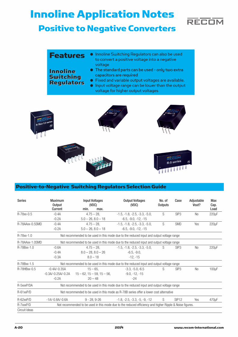
Series Maximum Input Voltages Output Voltages No. of Case Adjustable MaxOutput (VDC) (VDC) Outputs Vout? Cap.Current min. max. Load
R-78xx-0.5 -0.4A 4.75 – 28, -1.5, -1.8, -2.5, -3.3, -5.0, S SIP3 No 220µF-0.2A 5.0 – 26, 8.0 – 18 -6.5, -9.0, -12, -15
R-78AAxx-0.5SMD -0.4A 4.75 – 28, -1.5, -1.8, -2.5, -3.3, -5.0, S SMD Yes 220µF-0.2A 5.0 – 26, 8.0 – 18 -6.5, -9.0, -12, -15
R-78xx-1.0 Not recommended to be used in this mode due to the reduced input and output voltage range
R-78AAxx-1.0SMD Not recommended to be used in this mode due to the reduced input and output voltage range
R-78Bxx-1.0 -0.6A 4.75 – 28, -1.5, -1.8, -2.5, -3.3, -5.0, S SIP3 No 220µF-0.4A 8.0 – 28, 8.0 – 26 -6.5, -9.0,-0.3A 8.0 – 18 -12, -15
R-78Bxx-1.5 Not recommended to be used in this mode due to the reduced input and output voltage range
R-78HBxx-0.5 -0.4A/-0.35A 15 – 65, -3.3, -5.0,-6.5 S SIP3 No 100µF-0.3A/-0.25A/-0.2A 15 – 62, 15 – 59, 15 – 56, -9.0, -12, -15
-0.2A 20 – 48 -24
R-5xxxP/DA Not recommended to be used in this mode due to the reduced input and output voltage range
R-61xxP/D Not recommended to be used in this mode as R-78B series offer a lower cost alternative
R-62xxP/D -1A/-0.8A/-0.6A 9 - 28, 9-26 -1.8, -2.5, -3.3, -5, -9, -12 S SIP12 Yes 470µF
R-7xxxP/D Not recommended to be used in this mode due to the reduced efficiency and higher Ripple & Noise figures.
Circuit Ideas
● Innoline Switching Regulators can also be used to convert a positive voltage into a negative voltage
● The standard parts can be used - only two extra capacitors are required
● Fixed and variable output voltages are available.● Input voltage range can be lower than the output
voltage for higher output voltages
Positive-to-Negative Switching Regulators Selection Guide
Positive to Negative Converters
Innoline Application Notes
Features
InnolineInnolineSwitchingSwitchingRegulatorsRegulators
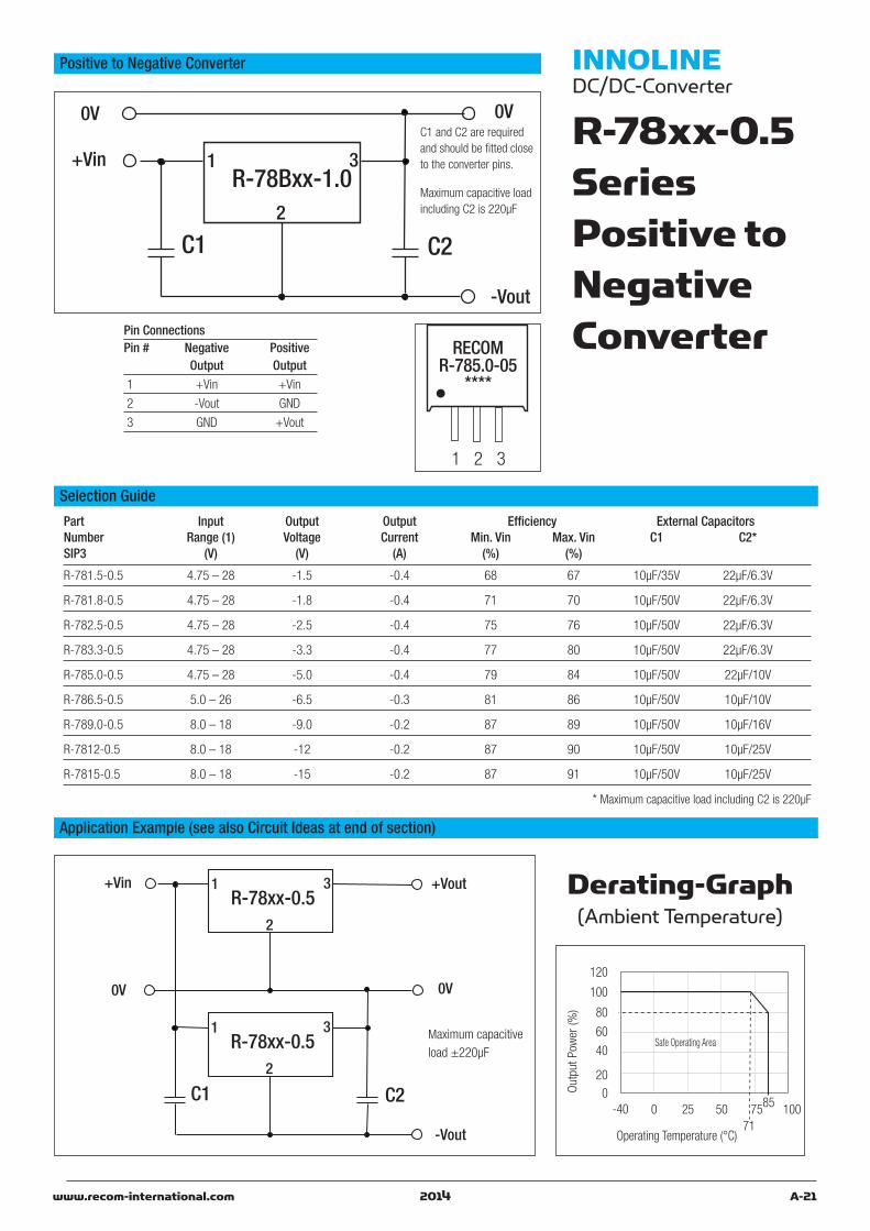
www.recom-international.com A-212014
INNOLINEDC/DC-Converter
R-78xx-0.5SeriesPositive toNegativeConverter
Selection Guide
Part Input Output Output Efficiency External CapacitorsNumber Range (1) Voltage Current Min. Vin Max. Vin C1 C2*SIP3 (V) (V) (A) (%) (%)
R-781.5-0.5 4.75 – 28 -1.5 -0.4 68 67 10µF/35V 22µF/6.3V
R-781.8-0.5 4.75 – 28 -1.8 -0.4 71 70 10µF/50V 22µF/6.3V
R-782.5-0.5 4.75 – 28 -2.5 -0.4 75 76 10µF/50V 22µF/6.3V
R-783.3-0.5 4.75 – 28 -3.3 -0.4 77 80 10µF/50V 22µF/6.3V
R-785.0-0.5 4.75 – 28 -5.0 -0.4 79 84 10µF/50V 22µF/10V
R-786.5-0.5 5.0 – 26 -6.5 -0.3 81 86 10µF/50V 10µF/10V
R-789.0-0.5 8.0 – 18 -9.0 -0.2 87 89 10µF/50V 10µF/16V
R-7812-0.5 8.0 – 18 -12 -0.2 87 90 10µF/50V 10µF/25V
R-7815-0.5 8.0 – 18 -15 -0.2 87 91 10µF/50V 10µF/25V
* Maximum capacitive load including C2 is 220µF
���1���,�=
�0��D
������
��
&�
���9 ��-�
�1�0����>�/�;1�0���0���E�
�
.�
�� 9�
"�2���1�0����>�'0��
.
-�
Derating-Graph(Ambient Temperature)
Application Example (see also Circuit Ideas at end of section)
Positive to Negative Converter
1� ����6$$���-
���+�
�� �'
-�-�
�
'
�
�� )
�#�)?����"�-�-"
GGGG
Pin ConnectionsPin # Negative Positive
Output Output1 +Vin +Vin
2 -Vout GND
3 GND +Vout
C1 and C2 are requiredand should be fitted closeto the converter pins.
Maximum capacitive loadincluding C2 is 220µF
����$$�-�"
���+�
�� �'
-�-�
�
'
�
1� ����$$�-�"
�
'
� 1��+�
Maximum capacitiveload ±220µF

A-22 www.recom-international.com2014
INNOLINEDC/DC-Converter
R-78AAxx-0.5 SMDPositive toNegativeConverter
Selection Guide
Part Input Output Output Efficiency External CapacitorsNumber Range (1) Voltage Current Min. Vin Max. Vin C1 C2SIP3 (V) (V) (A) (%) (%)
R-78AA1.5-0.5SMD 4.75 – 28 -1.5 -0.4 68 67 10µF/35V 22µF/6.3V
R-78AA1.8-0.5SMD 4.75 – 28 -1.8 -0.4 71 70 10µF/50V 22µF/6.3V
R-78AA2.5-0.5SMD 4.75 – 28 -2.5 -0.4 75 76 10µF/50V 22µF/6.3V
R-78AA3.3-0.5SMD 4.75 – 28 -3.3 -0.4 77 80 10µF/50V 22µF/6.3V
R-78AA5.0-0.5SMD 4.75 – 28 -5.0 -0.4 79 84 10µF/50V 22µF/10V
R-78AA6.5-0.5SMD 5.0 – 26 -6.5 -0.3 81 86 10µF/50V 10µF/10V
R-78AA9.0-0.5SMD 8.0 – 18 -9.0 -0.2 87 89 10µF/50V 10µF/16V
R-78AA12-0.5SMD 8.0 – 18 -12 -0.2 87 90 10µF/50V 10µF/25V
R-78AA15-0.5SMD 8.0 – 18 -15 -0.2 87 91 10µF/50V 10µF/25V
* Maximum capacitive load including C2 is 220µF
���1���,�=
�0��D
������
��
&�
���9 ��-�
�1�0����>�/�;1�0���0���E�
�
.�
�� 9�
"�2���1�0����>�'0��
.
-�
Derating-Graph(Ambient Temperature)
Application Example (see also Circuit Ideas at end of section)
Positive to Negative Converter
������$$�-�"?�
���+�
1�
-�
�F�
�� )F9.F+
&
-F
��
�') �)BB:��B��� 5���������+�;
��
-�
�'
�� 9
� -
�#�)?�����$$�-�"?�
�$$$$
� )
&.+Pin ConnectionsPin # Negative Positive
Output Output1,2 +Vin +Vin
3,7,8,9 -Vout GND
4,5 GND +Vout
6 -Vout Adj. +Vout Adj.
10 On/Off On/Off
C1 and C2 are requiredand should be fitted closeto the converter pins.
Maximum capacitive loadincluding C2 is 220µF
���+�
-�
�F�
�� )F9.F+
&
-F
��
�'
��
-�
�'
�����:�;$$�-�"?�
1� �F�
�� )F9.F+
&
-F
��
�'
1��+�
) �)BB
)&���5�+&���
)&���5�+&���
�����:�;$$�-�"?�
Maximum capacitiveload ±220µF

www.recom-international.com A-232014
���+�
�
�F�
�� )F9.F+
&
-F
�-/0
-�
''/0
�����:�;�'�-�"?�
� H�"���
�F�
�� )F9.F+
&
-F 1��+�
1"�
1!�
1�'�
1��"�
'�F
�--F
'--F
�"�
�!�
��'�
���"�
'�F
�--F
'--F
�������������� ��������������������������
1
�����:�;�'�-�"?�
Typical Application
Table 1: Adjustment Resistor Values
INNOLINEDC/DC-Converter R-78AAxx-0.5 SMD
Positive to Negative
0.5Adc R-78AA1.8 R-78AA2.5 R-78AA3.3 R-78AA5.0 R-78AA6.5 R-78AA9.0 R-78AA12-0.5SMD -0.5SMD -0.5SMD -0.5SMD -0.5SMD -0.5SMD -0.5SMD
Vout (nom.) 1.8Vdc 2.5Vdc 3.3Vdc 5.0Vdc 6.5Vdc 9.0Vdc 12.0Vdc
Vout (adj) R1 R2 R1 R2 R1 R2 R1 R2 R1 R2 R1 R2 R1 R2
-1.5 (V) 3KΩ 200Ω
-1.8 (V) 12KΩ
-2.5 (V) 11.8KΩ
-3.0 (V) 4.64KΩ 44.2KΩ 88.4KΩ 17KΩ
-3.3 (V) 27KΩ 6.7KΩ
-3.6 (V) 60.4KΩ 42KΩ 14KΩ
-3.9 (V) 28KΩ 58KΩ 23KΩ
-4.5 (V) 11.3kΩ 180KΩ 49KΩ 26KΩ 17KΩ
-4.9 (V) 7.15kΩ 850KΩ 77kΩ 36KΩ 24KΩ
-5.0 (V) 6.34kΩ 86kΩ 39KΩ 26KΩ
-5.1 (V) 5.9kΩ 231kΩ 97KΩ 42KΩ 28KΩ
-5.5 (V) 3.9kΩ 56.2kΩ 160KΩ 56KΩ 36KΩ
-6.5 (V) 14kΩ 112KΩ 63KΩ
-8.0 (V) 2.32kΩ 24.6KΩ 400KΩ 125KΩ
-9.0 (V) 10.7KΩ 200KΩ
-10 (V) 4.75KΩ 54.9KΩ 345KΩ
-11 (V) 1.65KΩ 16.5KΩ 740KΩ
-12 (V) 3.6KΩ
-12.6 (V) 0Ω 180KΩ

A-24 www.recom-international.com2014
INNOLINEDC/DC-Converter
R-78Bxx-1.0 SeriesPositive toNegativeConverter
Selection Guide
Part Input Output Output Efficiency External CapacitorsNumber Range (1) Voltage Current Min. Vin Max. Vin C1 C2*SIP3 (V) (V) (A) (%) (%)
R-78B1.5-1.0 4.75 – 28 -1.5 -0.6 70 68 10µF/50V 22µF/6.3V
R-78B1.8-1.0 4.75 – 28 -1.8 -0.6 72 72 10µF/50V 22µF/6.3V
R-78B2.5-1.0 4.75 – 28 -2.5 -0.6 75 77 10µF/50V 22µF/6.3V
R-78B3.3-1.0 4.75 – 28 -3.3 -0.6 77 80 10µF/50V 22µF/6.3V
R-78B5.0-1.0 6.5 – 28 -5.0 -0.6 83 85 10µF/50V 22µF/10V
R-78B6.5-1.0 8.0 – 26 -6.5 -0.4 84 87 10µF/50V 10µF/10V
R-78B9.0-1.0 8.0 – 18 -9.0 -0.4 88 89 10µF/25V 10µF/25V
R-78B12-1.0 8.0 – 18 -12 -0.3 89 90 10µF/25V 10µF/25V
R-78B15-1.0 8.0 – 18 -15 -0.3 89 91 10µF/25V 10µF/25V
* Maximum capacitive load including C2 is 220µF
���1���,�=
�0��D
������
��
&�
���9 ��-�
�1�0����>�/�;1�0���0���E�
�
.�
�� 9�
"�2���1�0����>�'0��
.
-�
Derating-Graph(Ambient Temperature)
Application Example (see also Circuit Ideas at end of section)
Positive to Negative Converter
1� ����6$$���-
���+�
�� �'
-�-�
�
'
�
�� )
�#�)?����6"�-���-
GGGG����������7
Pin ConnectionsPin # Negative Positive
Output Output1 +Vin +Vin
2 -Vout GND
3 GND +Vout
C1 and C2 are requiredand should be fitted closeto the converter pins.
Maximum capacitive loadincluding C2 is 220µF
����6$$���-
���+�
�� �'
-�-�
�
'
�
1� ����6$$���-
�
'
� 1��+�
Maximum capacitiveload ±220µF

A-25www.recom-international.com 2014
INNOLINEDC/DC-Converter
R-78Cxx-1.0 SeriesPositive toNegativeConverter
Selection Guide
Part Input Output Output Efficiency Number Range (1) Voltage Current Min. Vin Max. VinSIP3 (V) (V) (A) (%) (%)
R-78C1.8-1.0 5 – 38 -1.8 -0.8 69 70
R-78C3.3-1.0 7 – 37 -3.3 -0.8 77 80
R-78C5.0-1.0 8 – 35 -5.0 -0.7 79 83
R-78C9.0-1.0 12 – 31 -9.0 -0.6 85 87
R-78C12-1.0 15 – 28 -12 -0.5 87 89
R-78C15-1.0 18 – 25 -15 -0.5 89 90
���1���,�=
�0��D
������
��
&�
���9 ��-�
�1�0����>�/�;1�0���0���E�
�
.�
�� &.
"�2���1�0����>�'0��
.
-�
Derating-Graph(Ambient Temperature)
Application Example (see also Circuit Ideas at end of section)
Positive to Negative Converter
1� �����$$���-
���+�
�-/�"-�23�23�
�
'
�
�-/�"-���
�'G�
G'
�#�)?
>>>> �7
�� )
�#�)?�����"�-���-
GGGG
Pin ConnectionsPin # Negative Positive
Output Output1 +Vin +Vin
2 -Vout GND
3 GND +Vout
�����$$���-
���+�
�-/0�"-�
23��:��%;23�
�
'
�
1� �����$$���-
�
'
� 1��+�
�-/0�"-���
G'
G�
�'
.� (�� �I�J�K��+��J�+���)+�&+�9�:�*��5� ������9;
�#�)?
>>>> �7
>>>>
�#�)?
�7
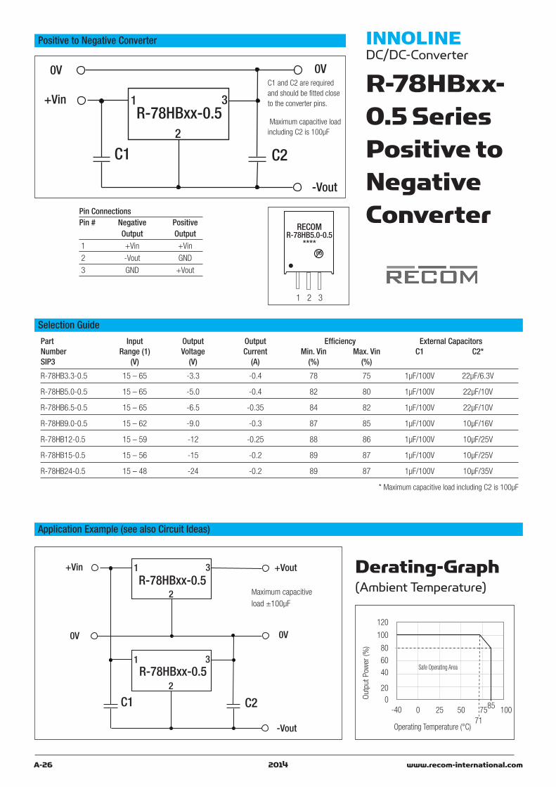
A-26 www.recom-international.com2014
INNOLINEDC/DC-Converter
R-78HBxx-0.5 SeriesPositive toNegativeConverter
Selection Guide
Part Input Output Output Efficiency External CapacitorsNumber Range (1) Voltage Current Min. Vin Max. Vin C1 C2*SIP3 (V) (V) (A) (%) (%)
R-78HB3.3-0.5 15 – 65 -3.3 -0.4 78 75 1µF/100V 22µF/6.3V
R-78HB5.0-0.5 15 – 65 -5.0 -0.4 82 80 1µF/100V 22µF/10V
R-78HB6.5-0.5 15 – 65 -6.5 -0.35 84 82 1µF/100V 22µF/10V
R-78HB9.0-0.5 15 – 62 -9.0 -0.3 87 85 1µF/100V 10µF/16V
R-78HB12-0.5 15 – 59 -12 -0.25 88 86 1µF/100V 10µF/25V
R-78HB15-0.5 15 – 56 -15 -0.2 89 87 1µF/100V 10µF/25V
R-78HB24-0.5 15 – 48 -24 -0.2 89 87 1µF/100V 10µF/35V
* Maximum capacitive load including C2 is 100µF
���1���,�=
�0��D
������
��
&�
���9 ��-�
�1�0����>�/�;1�0���0���E�
�
.�
�� 9�
"�2���1�0����>�'0��
.
-�
Derating-Graph(Ambient Temperature)
Application Example (see also Circuit Ideas)
Positive to Negative Converter
1� ����<6$$�-�"
���+�
�� �'
-�-�
�
'
�
�� )
�#�)?����<6"�-�-�"
GGGG����������7
Pin ConnectionsPin # Negative Positive
Output Output1 +Vin +Vin
2 -Vout GND
3 GND +Vout
C1 and C2 are requiredand should be fitted closeto the converter pins.
Maximum capacitive loadincluding C2 is 100µF
����<6$$�-�"
���+�
�� �'
-�-�
�
'
�
1� ����<6$$�-�"
�
'
� 1��+�
Maximum capacitiveload ±100µF

www.recom-international.com A-272014
Derating
';I�����/�;
1�0���0���E�
+�
&�
��
-�
�* ��*
����0����,�=�0������1�������#
�
.�.
�*9
Max output current calculation:Internal power dissipation (1W) = Io x Vo x (1-Efficiency)Io = 1(W) / Vo x (1-Efficiency)Example : R-625.0Pat Vin = +9VDC, Vout=-5.0VEfficiency = 80% (see ”Selection Guide” table)Io = 1W / 5V x (1-0.8) = -1000mAat Vin = +9VDC, Vout=-8.0V (with trim)Efficiency = 80% (see ”Selection Guide” table)Io = 1W / 8V x (1-0.8) = -625mA
Selection Guide
Part Input Output Output Efficiency External CapacitorsNumber Range (1) Voltage Current Min. Vin Max. Vin C1 C2*SIP3 (V) (V) (A) (%) (%)
R-621.8P/D 9 – 28 -1.8 (-1.5~-3.6) -1.0 72 65 10µF/50V 100µF/6.3V
R-622.5P/D 9 – 28 -2.5 (-1.5~-4.5) -1.0 76 72 10µF/50V 100µF/6.3V
R-623.3P/D 9 – 28 -3.3 (-1.8~-6V) -1.0 79 76 10µF/50V 100µF/10V
R-625.0P/D 9 – 28 -5.0 (-1.8~-9V) -1.0 81 80 10µF/50V 100µF/10V
R-629.0P/D 9 – 26 -9.0 (-3.3~-15V) -0.8 84 85 10µF/50V 100µF/25V
R-6212P/D 9 – 26 -12 (-3.3~-15V) -0.6 86 88 10µF/50V 100µF/25V
* Maximum capacitive load including C2 is 220µF
Positive to Negative Converter
���'$$���
���+�
1�
-�
�F)F-
� F&9F.
��
+F��F��
��
�'
) �)BB:��B��� 5���������+�;
��
-�
�'
������)��-�� ��&��9��.��+ ����������
� # � ) ?� � � ' � ' �
INNOLINEDC/DC-Converter
R-62xxP/DSIP12Positive toNegativeConverter
Pin ConnectionsPin # Negative Positive
Output Output2,3,4 +Vin +Vin
5,6,7,8 -Vout GND
9,10,11 GND +Vout
12 -Vout Adj. +Vout Adj.
1 On/Off On/Off
C1 and C2 are requiredand should be fitted closeto the converter pins.
Maximum capacitive loadincluding C2 is 220µF

A-28 www.recom-international.com2014
Remote On/Off Control Application Example
INNOLINEDC/DC-Converter
Table 1: Adjustment Resistor Values
-1Adc R-621.8P/D R-622.5P/D R-623.3P/D R-625.0P/D
Vout (nominal) 1.8VDC 2.5VDC 3.3VDC 5VDC
Vout (adj) R1 R2 R1 R2 R1 R2 R1 R2
1.5 13.6KΩ 3.3KΩ
1.8 8.2KΩ 3.1KΩ 820Ω
2.0 10KΩ 15KΩ 5.1KΩ 1.5KΩ
2.5 5.1KΩ 13KΩ 3.6KΩ
3.0 2.5KΩ 10KΩ 51KΩ 7.0KΩ
3.3 1.7KΩ 5.9KΩ 9.7KΩ
3.6 1.2KΩ 3.9KΩ 18KΩ 14KΩ
3.9 2.8KΩ 9.1KΩ 20KΩ
4.5 1.6KΩ 3.9KΩ 60KΩ
5.0 2.4KΩ
5.1 2.2KΩ 60KΩ
5.5 1.6KΩ 15KΩ
6.0 1.1KΩ 7.2KΩ
7.0 2.8KΩ
8.0 1.5KΩ
���+�
-�
��
�'
��
-�
�'
���$$$�1�
�F)F-
� F&9F.
��
+F��F��
��
�'
1��+�
) �)BB
)&���5�+&���
)&���5�+&���
���'$$�
�--/0
�F)F-
� F&9F.
��
+F��F�� Maximum capacitive
load ±220µF
R-62xxP_DPositive to Negative

www.recom-international.com A-292014
Positive to NegativeCircuit Ideas
Application Examples
INNOLINEDC/DC-Converter
��'�
����6�'���-
�'������--%�
�-/0�'"�
�-/0�'"�
-�
�
'
�
-�
1�� �����'�-�"
-�
�-/0�'"�
�-/0�'"�
���
�
'
�
�'��7����H�E���
�
����-"�-�"
�"������--%�
�-/0�'"�
''/0��-�
3
�
'
�
1�'�����""%�����-��'6 -�
%���
� 1�����
��
C�����5�%&�5����*� � 9���4+������� ��&����5����������+����+�&+��9+&&�,�
��/0����
�(
-��/0
��
��
��
�( ��
�.���&.�/��&���2,'�,' � 3
Negative Voltage Doubler
12V Battery Stabilisor
Negative Rail Generator for Asymmetric Rails

A-30 www.recom-international.com2014
Common Mode Chokes for EMC
Recom offers a range of Common Mode Chokes useful for EMI Filtering to meet the requirements of EN-55022, Class B.The component values given are suggested values and may need to be optimised to suit the application. The effectiveness of any filternetwork is heavily dependent on using quality capacitors, the layout of the board and having a low impedance path to ground. See section on filtering elsewhere in the Application Notes for more details.
� ���
���1����
��1��
�A�
�)
�-
����@�2�����������1���
Class B EMC Filter Suggestion
Powerline Application Notes
Powerline DC/DC ApplicationNotes● Common Mode Chokes for EMC
● Powerline Definitions and Testing
Introduction
Input Voltage Range
Pi Filter
Output Voltage Accuracy
Voltage Balance
Line Regulation
Load Regulation
Efficiency
Switching Frequency
Output Ripple and Noise
Transient Recovery Time
Current Limiting
Fold Back Current Limiting
Isolation
Break Down Voltage
Temperature Coefficient
Ambient Temperature
Operating Temperature Range
Storage Temperature Range
● Undervoltage Lockout Tables
● Output Voltage Trim Tables
● Powerline Heat Sinks
Heat Sink Dimensions
Powerline AC/DC ApplicationNotes
Input Fuse
Earthing
Combining Converters
DC Inputs
Contents
Standard EMC Filter
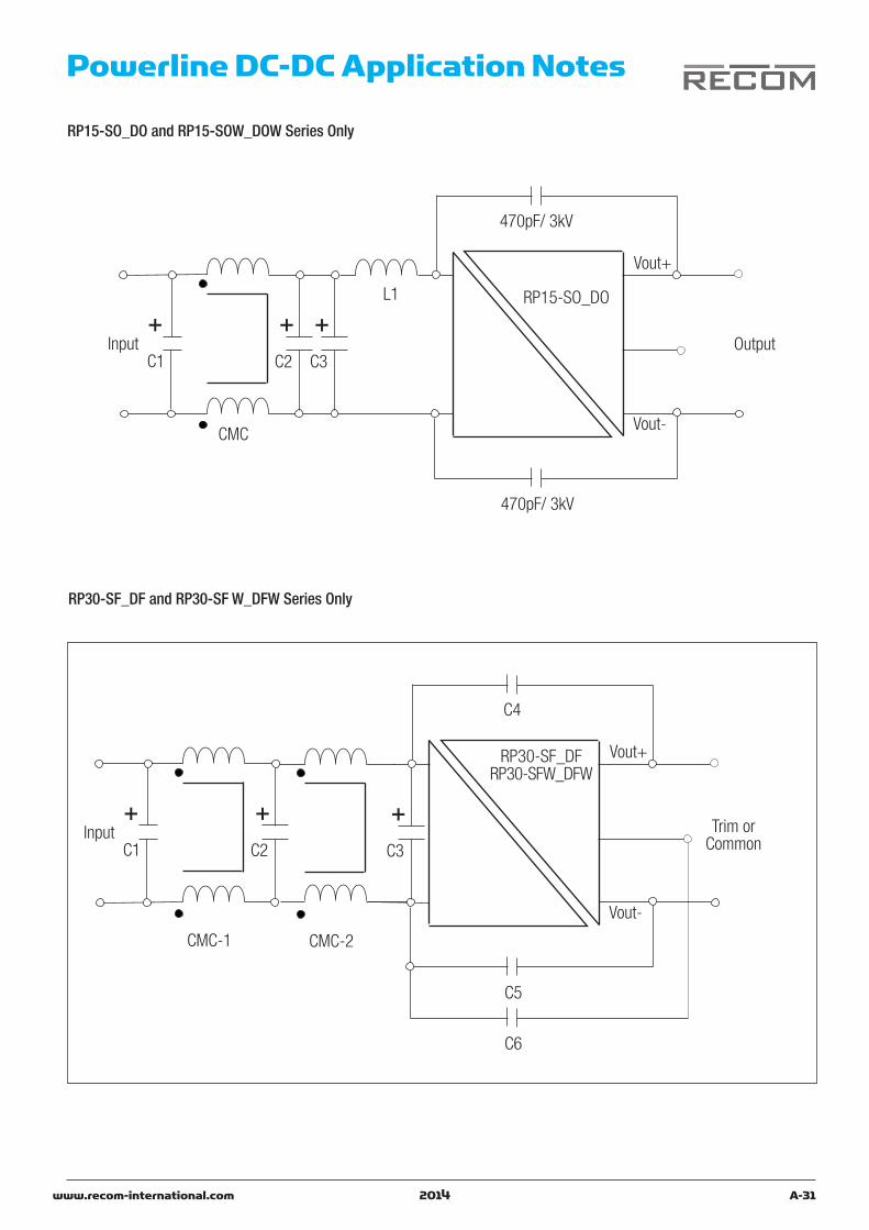
� � ���
/0�;��0��;;����
��1��
�A���
�
�-
�)
!,)��"@J�@!,)��"@#J�@#
�����
�����
�A���
�&
www.recom-international.com A-312014
Powerline DC-DC Application Notes
RP15-SO_DO and RP15-SOW_DOW Series Only
� � ���
���1����
��1��
�A�
-9�1@$�)��
-9�1@$�)��
�)
!,� �"�J��
�����
�����
��
RP30-SF_DF and RP30-SF W_DFW Series Only

A-32 www.recom-international.com2014
Component ValuesAll capacitors MLCC (Multi Layer Ceramic Capacitor).
RP08-A Vin = 12VDC nom., C1=4.7µF/50V, C2=Not Required, C3,C4=1nF/3kV, WE 7448229004 350µHVin = 24VDC nom., C1=6.8µF/50V, C2=Not Required, C3,C4=1nF/3kV, WE 7448229004 350µHVin = 48VDC nom., C1=2.2µF/100V, C2=2.2µF/100V, C3,C4=1nF/3kV, WE 7448229004 350µH
RP08-AW Vin = 9~36VDC, C1=4.7µF/50V, C2=Not Required, C3,C4=1nF/3kV, WE 7448229004 350µHVin = 18~75VDC, C1=2.2µF/100V, C2=2.2µF/100V, C3,C4=1nF/3kV, WE 7448229004 350µH
RP10-E Vin = 12VDC nom., C1=3.3µF/50V, C2=Not Required, C3,C4=1nF/2kV, WE 7448229004 350µHRP12-A Vin = 24VDC nom., C1=4.7µF/50V, C2=Not Required, C3,C4=1nF/2kV, WE 7448229004 350µH
Vin = 48VDC nom., C1=2.2µF/100V, C2=2.2µF/100V, C3,C4=1nF/2kV, WE 7448229004 350µH
RP10-EW Vin = 9~36VDC, C1=3.3µF/50V, C2=Not Required, C3,C4=1nF/2kV, WE 7448229004 350µHRP12-AW Vin = 18~75VDC, C1=2.2µF/100V, C2=2.2µF/100V, C3,C4=1nF/2kV, WE 74482210002 175µH
RP15-A Vin = 12VDC nom., C1=10µF/25V, C2=10µF/25V, C3,C4=470pF/2kV, WE 74482210002 175µHVin = 24VDC nom., C1=6.8µF/50V, C2=6.8µF/50V, C3,C4=470pF/2kV, WE 7448229004 350µHVin = 48VDC nom., C1=2.2µF/100V, C2=2.2µF/100V, C3,C4=470pF/2kV, WE 74466240007 700µH
RP15-AW Vin = 9~36VDC, C1=6.8µF/50V, C2=6.8µF/50V, C3,C4=470pF/2kV, WE 7448227005 450µHVin = 18~75VDC, C1=2.2µF/100V, C2=2.2µF/100V, C3,C4=470pF/2kV, WE 7448229004 350µH
RP15-O Vin = 12VDC nom., C1=10µF/25V, C2=10µF/25V, L1 = 10µH, WE 744822100002 175µHVin = 24VDC nom., C1=6.8µF/50V, C2=6.8µF/50V, L1 = 10µH, WE 744822100002 175µH Vin = 48VDC nom., C1=2.2µF/100V, C2=2.2µF/100V, L1 = 18µH, WE 744822100002 175µH
RP15-OW Vin = 9~36VDC, C1, C2, C3 =6.8µF/50V, WE 744822100002 175µHVin = 18~75VDC, C1=2 x 2.2µF/100V in parallel, C2,C3 =2.2µF/100V, L1 = 33µH, WE 7448229004 350µH
RP15-F Vin = 12VDC nom., C1=4.7µF/50V, C2=Not Required, C3,C4=1nF/2kV, WE 7448229004 350µHVin = 24VDC nom., C1=3.3µF/50V, C2=Not Required, C3,C4=1nF/2kV, WE 7448229004 350µHVin = 48VDC nom., C1=2.2µF/100V, C2=2.2µF/100V, C3,C4=1nF/2kV, WE 7448229004 350µH
RP15-FW Vin = 9~36VDC, C1=2.2µF/50V, C2=Not Required, C3,C4=1nF/2kV, WE 7448227005 450µHVin = 18~75VDC, C1=2.2µF/100V, C2=2.2µF/100V, C3,C4=1nF/2kV, WE 7448229004 350µH
RP20-F Vin = 12VDC nom., C1=4.7µF/50V, C2=Not Required, C3,C4=1nF/2kV, WE 7448227005 450µHVin = 24VDC nom., C1=4.7µF/50V, C2=Not Required, C3,C4=1nF/2kV, WE 7448227005 450µHVin = 48VDC nom., C1=2.2µF/100V, C2=2.2µF/100V, C3,C4=1nF/2kV, WE 7448227005 450µH
RP20-FW Vin = 9~36VDC, C1=4.7µF/50V, C2=Not Required, C3,C4=1nF/2kV, WE 7448227005 450µHVin = 18~75VDC, C1=2.2µF/100V, C2=2.2µF/100V, C3,C4=1nF/2kV, WE 7448229004 350µH
RP30-E Vin = 12VDC nom., C1=4.7µF/25V, C2=Not Required, C3,C4=1nF/2kV, WE 7448227005 450µHVin = 24VDC nom., C1=6.8µF/50V, C2=6.8µF/50V, C3,C4=1nF/2kV, WE 7448227005 450µHVin = 48VDC nom., C1=2.2µFII2.2µF/100V, C2=2.2µFII2.2µF/100V, C3,C4=1nF/2kV, WE 7448227005 450µH
RP30-EW Vin = 9~36VDC, C1=6.8µF/50V, C2=6.8µF/50V, C3,C4=1nF/2kV, WE 7448227005 450µHVin = 18~75VDC, C1=2.2µF II 2.2µF/100V, C2=2.2µF II 2.2µF/100V, C3,C4=1nF/2kV, WE 7448227005 450µH
Continued on next page
Powerline DC-DC Application Notes
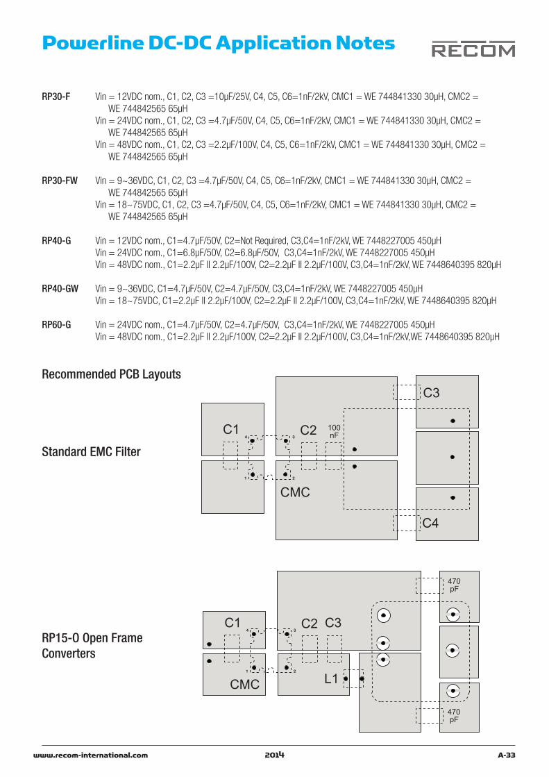
www.recom-international.com A-332014
Powerline DC-DC Application Notes
RP30-F Vin = 12VDC nom., C1, C2, C3 =10µF/25V, C4, C5, C6=1nF/2kV, CMC1 = WE 744841330 30µH, CMC2 = WE 744842565 65µH
Vin = 24VDC nom., C1, C2, C3 =4.7µF/50V, C4, C5, C6=1nF/2kV, CMC1 = WE 744841330 30µH, CMC2 = WE 744842565 65µH
Vin = 48VDC nom., C1, C2, C3 =2.2µF/100V, C4, C5, C6=1nF/2kV, CMC1 = WE 744841330 30µH, CMC2 = WE 744842565 65µH
RP30-FW Vin = 9~36VDC, C1, C2, C3 =4.7µF/50V, C4, C5, C6=1nF/2kV, CMC1 = WE 744841330 30µH, CMC2 = WE 744842565 65µH
Vin = 18~75VDC, C1, C2, C3 =4.7µF/50V, C4, C5, C6=1nF/2kV, CMC1 = WE 744841330 30µH, CMC2 = WE 744842565 65µH
RP40-G Vin = 12VDC nom., C1=4.7µF/50V, C2=Not Required, C3,C4=1nF/2kV, WE 7448227005 450µHVin = 24VDC nom., C1=6.8µF/50V, C2=6.8µF/50V, C3,C4=1nF/2kV, WE 7448227005 450µHVin = 48VDC nom., C1=2.2µF II 2.2µF/100V, C2=2.2µF II 2.2µF/100V, C3,C4=1nF/2kV, WE 7448640395 820µH
RP40-GW Vin = 9~36VDC, C1=4.7µF/50V, C2=4.7µF/50V, C3,C4=1nF/2kV, WE 7448227005 450µHVin = 18~75VDC, C1=2.2µF II 2.2µF/100V, C2=2.2µF II 2.2µF/100V, C3,C4=1nF/2kV, WE 7448640395 820µH
RP60-G Vin = 24VDC nom., C1=4.7µF/50V, C2=4.7µF/50V, C3,C4=1nF/2kV, WE 7448227005 450µHVin = 48VDC nom., C1=2.2µF II 2.2µF/100V, C2=2.2µF II 2.2µF/100V, C3,C4=1nF/2kV,WE 7448640395 820µH
��
� ��� ��
�(
��
�)�
���&��
Recommended PCB Layouts
Standard EMC Filter
RP15-O Open Frame Converters
��
� ��� �� �(
���)�
� �&!�
� �&!�

A-34 www.recom-international.com2014
Powerline DC-DC Application Notes
��
� ��� �� �(
�)� ���
� �
��
�4
�%
�)� �
Recommended PCB Layouts
RP30-S_DFRP30-S_DFW
General Information about Recom Common Mode Chokes
Recom common mode chokes are all RoHS conform. Maximum Rated Voltage = 500VDC
Operating Temperature = -40°C ~ +105°C

www.recom-international.com A-352014
Definitions and Testing
� �
� ������*��
�+�5�
������� ������+ ������9�
��
��
�������0��!A"� '3K����I��
���3
General Test Set-Up
Note: If the converter is under test withremote sense pins, connect these pins
to their respective output pins. All testsare made in ”Local sensing“ mode.
Figure 1-3: General DC/DC converter test set-up
Make and record the following measure-ments with rated output load at +25°C:
● Output voltage at nominal line (input) voltage. Vout N
● Output voltage at high line (input) voltage. Vout H
● Output voltage at low line (input)voltage. Vout L
The line regulation is Vout M (the maxi-mum of the two deviations of output) forthe value at nominal input in percentage.
Vout M – Vout N
Vout NX100
Line Regulations
The minimum and maximum input vol-tage limits within which a converter
will operate to specifications.
An input filter, consisting of two capacitors,connected before and after a seriesinductor to reduce input reflected ripplecurrent. The effective filter is C1/L+ L/C2, so the inductor filter element isdoubly effective.
Input Voltage Range
PI Filter
Output Voltage Accuracy
�
�����1��
����1��
Figure 2: PI Filter
With nominal input voltage and ratedoutput load from the test set-up, the DCoutput voltage is measured with anaccurate, calibrated DC voltmeter.Out put voltage accuracy is the differencebetween the measured output voltageand specified nominal value as apercentage. Output accuracy (as a %) isthen derived by the formula:
Vnom is the nominal output specified inthe converter data sheet.
Vout – Vnom
Vnom NX100
For a multiple output power converter,the percentage difference in the voltage
level of two outputs with opposite polar-rities and equal nominal values.
Voltage Balance
Powerline DC-DC Application Notes
A-36 www.recom-international.com2014
Definitions and Testing
Make and record the following measure-ments with rated output load at +25°C:
● Output voltage with rated load connected to the output. (Vout FL)
● Output voltage with no load or the minimum specified load for the
DC-DC converter. (Vout ML)
Load regulation is the difference be tweenthe two measured output voltages as apercentage of output voltage at ratedload.
The rate at which the DC voltage is swit-ched in a DC-DC converter or switchingpower supply. The ripple frequency is
double the switching frequency in push-pull designs.
Because of the high frequency contentof the ripple, special measurement tech-niques must be employed so that correctmeasurements are obtained. A 20MHzbandwidth oscilloscope is used, so thatall significant harmonics of the ripplespike are included.This noise pickup is eliminated as shownin Figure 3, by using a scope probe with
an external connection ground or ringand pressing this directly against theoutput common terminal of the powerconverter, while the tip contacts the vol-tage output terminal. This provides theshortest possible connection across theoutput terminals.
The ratio of output load power con sumptionto input power consumption expressedas a percentage. Normally measured at
full rated output power and nominal lineconditions.
Vout ML – Vout FL
Vout FLX100
Figure 3:
Load Regulation
Efficiency
Switching Frequency
Output Ripple and Noise
Powerline DC-DC Application Notes

www.recom-international.com A-372014
Figure 4 shows a complex ripple voltagewaveform that may be present on theoutput of a switching power supply.There are three components in the wa-veform, first is a charging component thatoriginates from the output rectifier andfilter, then there is the discharging com-ponent due to the load discharging theoutput capacitor between cycles, andfinally there are small high frequen cyswitching spikes imposed on the lowfrequency ripple.
,����,���';1����3�
/�;�
Figure 4: Amplitude
Output Ripple and Noise (continued)
Transient Recovery Time
Current Limiting
Fold Back Current Limiting
The time required for the power supplyoutput voltage to return to within a spe-ci fied percentage of rated value, follow -ing a step change in load current.
output current is limited to preventdamage of the converter at overloadsituations. If the output is shorted, the
output voltage is regulated down so thecurrent from the outputs cannot beexcessive.
A method of protecting a power supplyfrom damage in an overload condition,reducing the output current as the loadapproaches short circuit.
!���3���
�����
�����
Figure 6: Fold Back Current LimitingTime
���3
?�3�0�6���
�5�0�6���
�����
�����
�/�;�
/0�������!���5�04�/�;�
���1�������>�
����?
�
�����
?L��11�0���;���L���=�0���;��
Figure: 5 Transient Recovery Time
Definitions and Testing
Powerline DC-DC Application Notes

A-38 www.recom-international.com2014
The electrical separation between theinput and output of a converter, (con-sis ting of resistive and capacitive isola-
tion) normally determined by transfor-mer characteristics and circuit spacing.
The maximum continuous DC voltage,which may be applied between the inputand output terminal of a power supplywithout causing damage. Typical break-down voltage for DC-DCconverters is 1600VDC because theequivalent DC isolation for 230VACcontinuous rated working voltage is1500VDC.
With the power converter in a tempera-ture test chamber at full rated outputload, make the following measurements:
● Output voltage at +25°C ambient temperature.
● Set the chamber for maximum operating ambient temperature and allow the power converter to stabilize for 15 to 30 minutes. Measure the output voltage.
● Set the chamber to minimum operating ambient temperature and allow the power converter to stabilize for 15 to 30 minutes.
● Divide each percentage voltage deviation from the +25°C ambient value by the corresponding tempe-rature change from +25°C ambient.
The temperature coefficient is the higherone of the two values calculated above,expressed as percent per change centi-grade.
���1��!����2��0��3
!�>�����0��1��
�0���3�=�������>�
!������5����3��1�����5�����������
�
!
Isolation
Break-Down Voltage
Temperature Coefficient
Ambient Temperature
Operating Temperature Range
Storage Temperature Range
Figure 7:
The temperature of the still-air im-mediately surrouding an operatingpower supply. Care should be takenwhen comparing manufacturer’s da-
ta sheets that still-air ambient tempe-rature and not case temperature isquoted.
The range of ambient or case tempe-rature within a power supply at which
it operates safely and meets itsspecifications.
The range of ambient temperatureswithin a power supply at non-opera-
ting condition, with no degradation inits subsequent operation.
Definitions and Testing
Powerline DC-DC Application Notes

www.recom-international.com A-392014
Some converters from our Powerline offerthe feature of trimming the output voltage ina certain range around the nominal valueby using external trim resistors.Because different series use different cir-cuits for trimming, no general equation canbe given for calculating the trim resistors.
The following trimtables give values forchosing these trimming resistors. If voltages between the given trim pointsare required, extrapolate between the twonearest given values to work out the re-sis tor required or use a variable resistor toset the voltage.
Output Voltage Trimming:
Trim up 1 2 3 4 5 6 7 8 9 10 %
Vout = 3,333 3,366 3,399 3,432 3,465 3,498 3,531 3,564 3,597 3,63 Volts
RU = 57.93 26.16 15.58 10.28 7.11 4.99 3.48 2.34 1.46 0.75 KOhms
Trim down 1 2 3 4 5 6 7 8 9 10 %
Vout = 3,267 3,234 3,201 3,168 3,135 3,102 3,069 3,036 3,003 2,97 Volts
RD = 69.47 31.23 18.49 12.12 8.29 5.74 3.92 2.56 1.50 0.65 KOhms
RP15-, RP20-, RP30-, RP40-, RP60- xx3.3S (For RP15-SA/SAW and RP15-SO/SOW see next page)
Trim up 1 2 3 4 5 6 7 8 9 10 %
Vout = 5,05 5,1 5,15 5,2 5,25 5,3 5,35 5,4 5,45 5,5 Volts
RU = 36.57 16.58 9.92 6.58 4.59 3.25 2.30 1.59 1.03 0.59 KOhms
Trim down 1 2 3 4 5 6 7 8 9 10 %
Vout = 4,95 4,9 4,85 4,8 4,75 4,7 4,65 4,6 4,55 4,5 Volts
RD = 45.53 20.61 12.31 8.15 5.66 4.00 2.81 1.92 1.23 0.68 KOhms
RP15-, RP20-, RP30-, RP40-, RP60- xx05S (For RP15-SA/SAW and RP15-SO/SOW see next page)
Trim up 1 2 3 4 5 6 7 8 9 10 %
Vout = 12,12 12,24 12,36 12,48 12,6 12,72 12,84 12,96 13,08 13,2 Volts
RU = 367.91 165.95 98.64 64.98 44.78 31.32 21.70 14.49 8.88 4.39 KOhms
Trim down 1 2 3 4 5 6 7 8 9 10 %
Vout = 11,88 11,76 11,64 11,52 11,4 11,28 11,16 11,04 10,92 10,8 Volts
RD = 460.99 207.95 123.60 81.42 56.12 39.25 27.20 18.16 11.13 5.51 KOhms
RP15-, RP20-, RP30-, RP40- ,RP60-xx12S (For RP15-SA/SAW and RP15-SO/SOW see next page)
Trim up 1 2 3 4 5 6 7 8 9 10 %
Vout = 15,15 15,3 15,45 15,6 15,75 15,9 16,05 16,2 16,35 16,5 Volts
RU = 404.18 180.59 106.06 68.80 46.44 31.53 20.88 12.90 6.69 1.72 KOhms
Trim down 1 2 3 4 5 6 7 8 9 10 %
Vout = 14,85 14,7 14,55 14,4 14,25 14,1 13,95 13,8 13,65 13,5 Volts
RD = 499.82 223.41 131.27 85.20 57.56 39.14 25.97 16.10 8.42 2.282 KOhms
RP15-, RP20-, RP30-, RP40-, RP60- xx15S (For RP15-SA/SAW and RP15-SO/SOW see next page)
Single Output Voltage Trim Tables
Trim Tables
Powerline DC-DC Application Notes
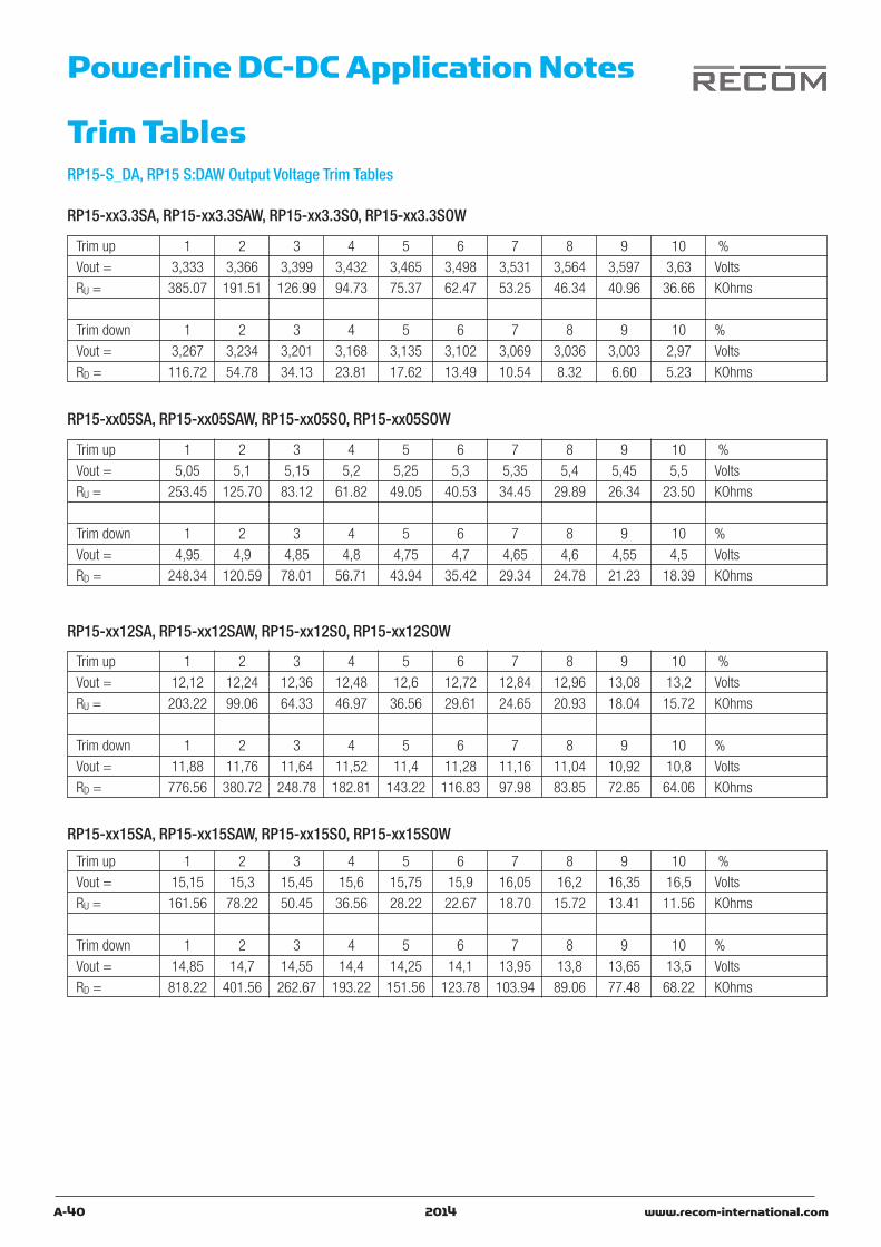
A-40 www.recom-international.com2014
Trim up 1 2 3 4 5 6 7 8 9 10 %
Vout = 3,333 3,366 3,399 3,432 3,465 3,498 3,531 3,564 3,597 3,63 Volts
RU = 385.07 191.51 126.99 94.73 75.37 62.47 53.25 46.34 40.96 36.66 KOhms
Trim down 1 2 3 4 5 6 7 8 9 10 %
Vout = 3,267 3,234 3,201 3,168 3,135 3,102 3,069 3,036 3,003 2,97 Volts
RD = 116.72 54.78 34.13 23.81 17.62 13.49 10.54 8.32 6.60 5.23 KOhms
RP15-xx3.3SA, RP15-xx3.3SAW, RP15-xx3.3SO, RP15-xx3.3SOW
Trim up 1 2 3 4 5 6 7 8 9 10 %
Vout = 5,05 5,1 5,15 5,2 5,25 5,3 5,35 5,4 5,45 5,5 Volts
RU = 253.45 125.70 83.12 61.82 49.05 40.53 34.45 29.89 26.34 23.50 KOhms
Trim down 1 2 3 4 5 6 7 8 9 10 %
Vout = 4,95 4,9 4,85 4,8 4,75 4,7 4,65 4,6 4,55 4,5 Volts
RD = 248.34 120.59 78.01 56.71 43.94 35.42 29.34 24.78 21.23 18.39 KOhms
RP15-xx05SA, RP15-xx05SAW, RP15-xx05SO, RP15-xx05SOW
Trim up 1 2 3 4 5 6 7 8 9 10 %
Vout = 12,12 12,24 12,36 12,48 12,6 12,72 12,84 12,96 13,08 13,2 Volts
RU = 203.22 99.06 64.33 46.97 36.56 29.61 24.65 20.93 18.04 15.72 KOhms
Trim down 1 2 3 4 5 6 7 8 9 10 %
Vout = 11,88 11,76 11,64 11,52 11,4 11,28 11,16 11,04 10,92 10,8 Volts
RD = 776.56 380.72 248.78 182.81 143.22 116.83 97.98 83.85 72.85 64.06 KOhms
RP15-xx12SA, RP15-xx12SAW, RP15-xx12SO, RP15-xx12SOW
Trim up 1 2 3 4 5 6 7 8 9 10 %
Vout = 15,15 15,3 15,45 15,6 15,75 15,9 16,05 16,2 16,35 16,5 Volts
RU = 161.56 78.22 50.45 36.56 28.22 22.67 18.70 15.72 13.41 11.56 KOhms
Trim down 1 2 3 4 5 6 7 8 9 10 %
Vout = 14,85 14,7 14,55 14,4 14,25 14,1 13,95 13,8 13,65 13,5 Volts
RD = 818.22 401.56 262.67 193.22 151.56 123.78 103.94 89.06 77.48 68.22 KOhms
RP15-xx15SA, RP15-xx15SAW, RP15-xx15SO, RP15-xx15SOW
RP15-S_DA, RP15 S:DAW Output Voltage Trim Tables
Trim Tables
Powerline DC-DC Application Notes

www.recom-international.com A-412014
Trim up 1 2 3 4 5 6 7 8 9 10 %
Vout = 24,24 24,48 24,72 24,96 25,2 25,44 25,68 25,92 26,16 26,4 Volts
RU = 218.21 98.10 58.07 38.05 26.04 18.03 12.32 8.03 4.69 2.02 KOhms
Trim down 1 2 3 4 5 6 7 8 9 10 %
Vout = 23,76 23,52 23,28 23,04 22,8 22,56 22,32 22,08 21,84 21,6 Volts
RD = 273.44 123.02 72.87 47.80 32.76 22.73 15.57 10.20 6.02 2.67 KOhms
RP15-, RP20, RP30-, RP40- xx12D
Trim up 1 2 3 4 5 6 7 8 9 10 %
Vout = 30,3 30,6 30,9 31,2 31,5 31,8 32,1 32,4 32,7 33 Volts
RU = 268.29 120.64 71.43 46.82 32.06 22.21 15.1 9.91 5.81 2.53 KOhms
Trim down 1 2 3 4 5 6 7 8 9 10 %
Vout = 29,7 29,4 29,1 28,8 28,5 28,2 27,9 27,6 27,3 27 Volts
RD = 337.71 152.02 90.13 59.18 40.61 28.23 19.39 12.76 7.60 3.47 KOhms
RP15-, RP20-, RP30-, RP40- xx15D
Dual Output Voltage Trim Tables
Trim Tables
Powerline DC-DC Application Notes

A-42 www.recom-international.com2014
Undervoltage Lockout Tables
At low input voltages, the input currentscan exceed the rating of the converter.Therefore, converters featuring under-
voltage lockout will automitically shutdown if the input voltage is too low. Asthe input voltage rises, they will restart.
Undervoltage Lockout
Converter Series Nominal Input Voltage Switch ON Switch OFFinput voltage input voltage
RP08-S_DAW 24V (9~36VDC) 9VDC 8VDC
48V (18~75VDC) 18VDC 16VDC
RP12-S_DA 12V (9~18VDC) 9VDC 8VDC
24V (18~36VDC) 18VDC 16VDC
48V (36~75VDC) 36VDC 33VDC
RP12-S_DAW 24V (9~36VDC) 9VDC 8VDC
48V (18~75VDC) 18VDC 16VDC
RP15-S_DA, RP15-S_DO 12V (9~18VDC) 9VDC 8VDC
24V (18~36VDC) 17VDC 14.5VDC
48V (36~75VDC) 33VDC 30.5VDC
RP15-S_DAW, RP15-S_DOW 24V (9~36VDC) 9VDC 8VDC
48V (18~75VDC) 18VDC 16VDC
RP15-S_DFW 24V (9~36VDC) 9VDC 7.5VDC
48V (18~75VDC) 18VDC 15VDC
RP20-S_DFW 24V (9~36VDC) 9VDC 7.5VDC
48V (18~75VDC) 18VDC 15VDC
RP30-S_DE 12V (9~18VDC) 9VDC 8VDC
24V (18~36VDC) 17.8VDC 16VDC
48V (36~75VDC) 36VDC 33VDC
RP30-S_DEW 24V (10~40VDC) 10VDC 8VDC
48V (18~75VDC) 18VDC 16VDC
RP40-S_D_TG 12V (9~18VDC) 9VDC 8VDC
24V (18~36VDC) 17.8VDC 16VDC
48V (36~75VDC) 36VDC 34VDC
RP30-S_DGW 24V (9~36VDC) 9VDC 8VDC
48V (18~75VDC) 18VDC 16VDC
RP60-SG 24V (18~36VDC) 17VDC 15VDC
48V (36~75VDC) 34VDC 32VDC
Undervoltage Lockout
Powerline DC-DC Application Notes

www.recom-international.com A-432014
DC-DC Converter Applications
Thermal Management-The Laws of Thermodynamics
Smaller, more powerful, better performance…are the buzzwords in the area of DC/DCmodule power supplies. Good thermalmanagement of the heat generated hasbecome an important part of the design-process. But what needs to be done?
An indisputable fact is that the efficiency of anyenergy conversion process is always less than100%. This means that a part of the energybeing converted goes astray as heat and thatultimately this waste heat must be removed.The laws of thermodynamics state that heatenergy can only flow from a warmer to acolder environment. So, for DC/DC converters,this means that if the internal heat is to bedissipated out of the module, that the ambienttemperature must always be lower than themaximum allowable internal temperature. Thelarger this difference, the more effectivelywaste heat can flow out of the converter.
But which temperature specifications in thedatasheets are to be consulted for the thermalcalculations? RECOM declares two values inits datasheets, Operating Temperature Range(with or without derating) and the MaximumCase Temperature. Some manufacturers evenclaim that these two values are the same.
The case (surface) temperature of DC/DCmodules are typically given as around +100°C.This value appears at first to be very high;however this figure includes not only the self-warming through internal losses but also theambient temperature itself.
Remember: The smaller the differencebetween case surface and ambient, so thesmaller the amount of heat that can be lost tothe surroundings. If a converter has highinternal dissipation, then it will be moreaffected by a small temperature differencethan a converter with low internal dissipation.The internal losses occur mainly throughswitching losses in the transistors, rectificationlosses, core losses in the transformer andresistive losses in the windings and tracks. Themaximum allowable internal temperature isdetermined by either the curie temperature ofthe transformer core material, the maximumjunction temperature of the switchingtransistors or rectification diodes or themaximum operating temperature of thecapacitors: whichever is the lowest.
Thermal Management-Thermal Impedance
The Thermal Impedance is a measure of howeffectively heat can flow from inside the con-verter to its surroundings. It is measured in°C/Watt. It is possible to further lower thethermal resistance to ambient by fitting anexternal heat sink as this increases the surfacearea from which heat can be transferred to thesurrounding air. The thermal impedance canalso be lowered by blowing air across theconverter as moving air can transfer more heataway from the converter as stationary air.
Recom datasheets always show the thermalimpedance without a heatsink and withnatural convection (still air).
The datasheets also state the minimum andmaximum ambient operating temperaturerather than just the maximum casetemperature because this is easiest for the enduser to measure and to monitor. The advantageis that true ambient temperature can be mea-sured in the actual application and it need notbe calculated theoretically, plus the results arevalid for both sealed and vented constructionswith a through-flow of cooling air.
Nevertheless, the maximum case temperatureis useful to decide on a suitably dimensionedheat sink so that the maximum casetemperature is not exceeded at the maximumambient temperature.
The internal losses and thermal resistancescan also be derived mathematically. For the calculations, Ohm’s Law of R=V/I canbe modified so that R becomes thermal resi-stance, V becomes temperature and I becomespower dissipation. The following equations canthus be derived:
whereR THcase-ambient = Thermal impedance (from the case to the ambient surroundings)T case =Case temperatureT ambient=Environment temperature P dissipation =Internal losses P in =Input power P out =Output power η(oper) =efficiency under the given operating
conditions
With help of the above formulae, the maximumallowable ambient temperature for a given setof operating conditions can be calculated - butit is important to remember that efficiency isdependent on both the output load and theinput voltage.
The formulae also demonstrate that casetemperature is not the same as operatingtemperature, as is so often falsely claimed.
A practical example:Take the RP30-4805SE with 80% load:What is the maximum operating temp?
From the datasheet text and graphs, thefollowing information can be found:R THcase-ambient = 10°C/WT case = 100°C maximumT ambient=unknown
P dissipation must be calculated from:P out = 30 x 80% = 24Wη(oper) = 90% (from Eff vs Load Graph)
P diss. = 24/0.9 -24 = 2.66 Watts.
Thus10W/°C = (100 - T amb) / 2.66Wand T amb max. = 73.4°C
At 100% load, this figure reduces to 64.4°C
At 100% load and over the full input voltagerange, this figure reduces further to 59.1°C
If the thermal dissipation calculations revealthat the DC/DC Module will overheat at thedesired ambient operating temperature, thenthere are still a number of options available toreach a solution.
One option is to derate the converter, i.e, use ahigher power converter running at less than fullload. The derating diagrams in the datasheetsessentially define the maximum load at anygiven temperature within the operatingtemperature range. The derating curves are inreality not so linear as they are declared inmost datasheets. However, reliablemanufacturers will always err on the safe sideso that the values given can be safely relied onin practice.
If the converter has a plastic case, then thenext largest case size with the same powerrating could be chosen to increase theavailable surface area. However, care must betaken not to compromise on efficiencyotherwise no net gain will be made.

A-44 www.recom-international.com2014
Thermal Management-Heat Sinking
If the converter has a metal case, then addinga heat sink is can be very effective, particularlyin conjunction with a forced-air cooling system.If a heat sink is used with fan cooling, then thethermal resistance equation becomes:
RTHcase-ambient = RTHcase-heatsink + RTHheatsink-ambient
whereRTHcase-ambient =Thermal impedance
(from the case to the ambient surroundings)
RTHcase-heatsink =Thermal impedance
(from the case to the heat sink)
RTHheatsink-ambient =Thermal impedance
(from the heat sink to ambient)
The value of RTH heatsink-ambient includesthe thermal resistance of the heat sink as wellas the thermal resistance of any thermallyconductive paste or silicon pads used for abetter thermal contact to the case. If these heattransfer aids are not applied, then a value ofapproximately 0.2 K/W must be added to thethermal resistance of the heat sink alone.When establishing of the value of RTHheatsink-ambient it is also necessary to knowhow much air is being blown across the heatsink fins. These values are most often given inlfm (linear feet per minute) and declared by thefan manufacturer. The conversion to m/s is100lfm = 0.5 m/s.
Calculation of heatsinks size:
Example: RP30-2405SEW starts deratingwith out heatsink at +65°C but the desiredoperation is 30W at +75°C so the size ofthe heatsink has to be calculated.
Pout = 30WEfficiency = 88% max.Pd = Pout - Pout = 30W - 30W = 4.1W
Efficiency 88%Tcase = 100°C (max. allowed case temperature)
Tambient = 75°C
RTHcase-ambient = Tcase-Tambient = 100°C-75°CPD 4.1W
=6.1°C/W
So it has to be ensured that the thermalresis tance between case and ambient is6,1°C/W max.
When mounting a heatsink on a case there isa thermal resistance RTH case-heatsink be tweencase and heatsink which can be reduced byusing thermal conductivity paste but cannot beeliminated totally.
Therefore, If a heatsink is mounted on theconverter, it’s thermal resistance has to be atleast:
RTHcase-ambient = RTHcase-heatsink + RTHheatsink-ambient =6.1°C/W - 1°C/W = 5.1°C/W
If however, the results of your calculations ormeasurements are border-line, then the issuemust be examined in more depth. So, forexample, there is a difference in thermalperformance between vertically andhorizontally mounted modules, between staticair and freely convecting air and with air at lowatmospheric pressures.
Heatsink mounted on casewithout thermal conductivity paste RTH case-heatsink = ca. 1…2 °C/W
Heatsink mounted on case
with thermal conductivity paste RTH case-heatsink = ca. 0,5…1 °C/W
Heatsink mounted on case with thermal conductivity paste and electrical isolation film RTH case-heatsink = ca. 1…1,5 °C/W
���� ���� 3��� ����� ����� 3����
�1�
�13
�1%
�1�
�1�
�1��
.������&5��6
�.��.�&��������
�������������
DC-DC Converter Applications
www.recom-international.com A-452014
��(��
��(���:�"�(��%%;
�*)�
�*)�
�*)�
�*-�
�*��
�*-�
-+*.��M�*�
�-*��M�*� ��*���M�*�
��*���M�*�
!��*&
�*��M�*�
)*��M�*�
*&��M�*�
�*9��M�*�
!��
7G-0020C (9.5°C/W) - includes double-sided adhesive pad and clips
7G-0047C (12°C/W)- includes double-sided adhesive pad and clips
Heat Sinks available from Recom
Powerline DC-DC Application Notes

A-46 www.recom-international.com2014
7G-0011C (8.24°C/W)- includes double-sided adhesive pad and clips
��(��
��(���:�"�(��%%;
�*)�
�*)�
�*-�
�*��
�*��
�*���M�*�
)9*-�M�*�
�9*���M�*�
*&��M�*�
�*9��M�*�
� *���M�*�
)*���M�*�
!��*&
��(��
��(���:�"�(��%%;
�*)�
�*)�
�*)�
�*-�
�*)�
�*-�
-+*.��M�*�
-+*.��M�*� ��*���M�*�
��*���M�*�!��*&
�*��M�*�
)*��M�*�
*&��M�*�
�*9��M�*�
7G-0026C (7.8°C/W)- includes double-sided adhesive pad and clips
Heat Sinks available from Recom
Powerline DC-DC Application Notes

www.recom-international.com A-472014
AC/DC Application Notes
������� ������
�
'3K����I�����3
/�;������4@���
�����
������
������� ������
�
'3K����I�����3
/�;������4@����
�����
������
��5�
���0��
'��,?/
Input Fuse
Note: An input fuse is recommended forsafety and protection. A time-delay or slo-blo fuse should befitted. If the AC connector is not-polarised, thenfuses can be fitted to both inputs
Recommended Fuse Ratings<40W 1.5Amp 40W 2 Amp60W 3 Amp
������� ������
�
'3K����I��
���3
/�;������4@���
�����
������
��5�
���0��
��0�6 @
�1�����������
Earthing
Note: If the converter has a ground pin(FG), then it must be earthed to a safetyground point.
Use thicker,shorter cables to ensure agood connection as this will also reducethe EMC interference.-Vout can be also connected to FG to re-ference the output to Ground.
������� ������
�
'3K����I��
���3
/�;������4@���
�����
������
��5�
���0��
��0�6 @
� �0 ����
External Filter
Note: The RECOM RAC series contain abuilt-in line filter to meet EN 55022 ClassB Conducted Emissions.
If additional filtering is required, then anexternal line filter module can be fitted.The cabling between the external filterand the converter should be kept asshort as possible and a central star-earthwiring should be used.

A-48 www.recom-international.com2014
AC/DC Application Notes
��
��
��
��
���
���
��
��
���
�
��
��
��
��
���
��
��
��
���
�
Combining Converters
-in Parallel
Note: AC/DC converters can beparalleled to increase the output voltageor to make a hot-swap circuit.The inputs of two AC/DC converters can-not be wired in series to increase theinput voltage range.However, single phase AC/DC converterscan be used with three phase supplies ifthe input is connected via diodes.
������� ������
�
A������3
/�;������4@���
�����
��
��5�
���0��
��0�6 @
����$$
'�7*���3
������� ������
�
A������3
/�;������4@���
�����
��
��5�
���0��
��0�6 @
��
�����
�����
Note: A DC/DC converter or switchingregulator can be powered from theoutput of an AC/DC converter to add anauxilliary output or negative rail.
������� ������
�
'3K����I�����3
/�;������4@���
�����
������
������
DC Inputs
Note: All AC/DC converters will also workwith DC inputs.Check the individual datasheets for theDC input voltage ranges.
Combining Converters
-in Series
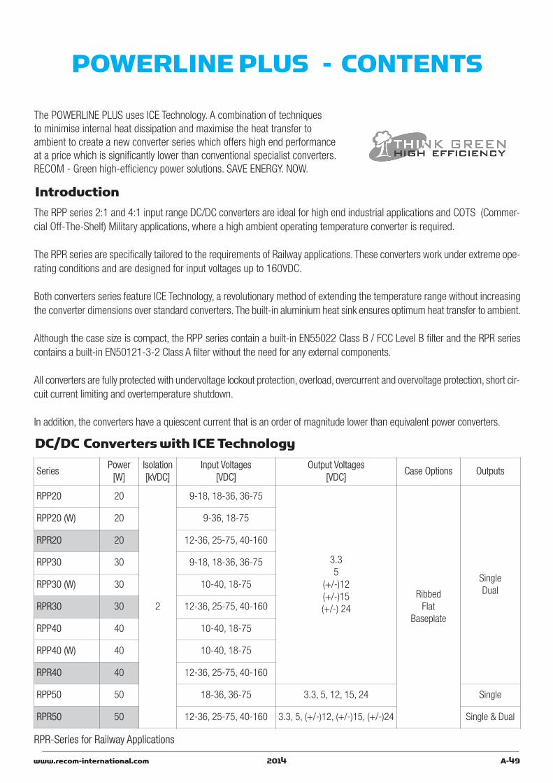
A-49www.recom-international.com 2014
The RPP series 2:1 and 4:1 input range DC/DC converters are ideal for high end industrial applications and COTS (Commer-cial Off-The-Shelf) Military applications, where a high ambient operating temperature converter is required.
The RPR series are specifically tailored to the requirements of Railway applications. These converters work under extreme ope-rating conditions and are designed for input voltages up to 160VDC.
Both converters series feature ICE Technology, a revolutionary method of extending the temperature range without increasingthe converter dimensions over standard converters. The built-in aluminium heat sink ensures optimum heat transfer to ambient.
Although the case size is compact, the RPP series contain a built-in EN55022 Class B / FCC Level B filter and the RPR seriescontains a built-in EN50121-3-2 Class A filter without the need for any external components.
All converters are fully protected with undervoltage lockout protection, overload, overcurrent and overvoltage protection, short cir-cuit current limiting and overtemperature shutdown.
In addition, the converters have a quiescent current that is an order of magnitude lower than equivalent power converters.
POWERLINE PLUS - CONTENTS
DC/DC Converters with ICE Technology
Introduction
The POWERLINE PLUS uses ICE Technology. A combination of techniquesto minimise internal heat dissipation and maximise the heat transfer toambient to create a new converter series which offers high end performanceat a price which is significantly lower than conventional specialist converters.RECOM - Green high-efficiency power solutions. SAVE ENERGY. NOW.
RPR-Series for Railway Applications
SeriesPower
[W]Isolation[kVDC]
Input Voltages[VDC]
Output Voltages[VDC]
Case Options Outputs
RPP20 20
2
9-18, 18-36, 36-75
3.35
(+/-)12 (+/-)15(+/-) 24
RibbedFlat
Baseplate
SingleDual
RPP20 (W) 20 9-36, 18-75
RPR20 20 12-36, 25-75, 40-160
RPP30 30 9-18, 18-36, 36-75
RPP30 (W) 30 10-40, 18-75
RPR30 30 12-36, 25-75, 40-160
RPP40 40 10-40, 18-75
RPP40 (W) 40 10-40, 18-75
RPR40 40 12-36, 25-75, 40-160
RPP50 50 18-36, 36-75 3.3, 5, 12, 15, 24 Single
RPR50 50 12-36, 25-75, 40-160 3.3, 5, (+/-)12, (+/-)15, (+/-)24 Single & Dual

www.recom-international.comA-50 2014
I.C.E TechnologyICE (Innovation in Converter Excellence)Technology uses a combination of techniquesto minimise internal heat dissipation andmaximise the heat transfer to ambient tocreate a new converter series which offers highend performance at a price which is signifi-cantly lower than conventional specialist con-verters.The exact details of this technology mustremain secret, but the following brief resumedescribes the main features of thistechnological breakthrough:
Minimising internal heat dissipationThe difference between the input power andthe output power is the internal powerdissipation which generates heat within theconverter.If the converter is inefficient at convertingpower, then adding external heat sinks, base-plates or fans are remedies that cure thesymptoms rather than address the illness.First and foremost, the converter must have thehighest possible efficiency over the entire inputvoltage range and load conditions. Most powerconverters are designed to be most efficient at25°C, full load and nominal input voltage andthus offer a compromise performance whenlightly loaded or operated at the maximumambient temperature.ICE Technology uses state-of-the-arttechniques to improve power convertionefficiency by approximately 2% compared tostandard converters. A two per cent improve-ment may not sound much, but the differencebetween a converter with 88% efficiency andone with 90% efficiency is a 17% reduction inthe dissipated power. In addition, when lightlyloaded, the converters enter a power savingmode and draw only a few milliamps from thesupply.
Maximising heat transferThe rate of heat transfer between a hot bodyand its cooler surroundings is given byFourier’s Law: q=-k.ΔTwhere q = rate of heat transferk = thermal conductivityand ΔT = temperature difference
If k can be made larger, then the rate of heattransfer can still match or exceed the rate ofheat generation at lower temperaturedifferences ΔT and the converter will have anextended operating temperature range.
Techniques to improve thermalconductivity
ICE Technology splits the thermal conductivityproblem into two areas and attacks each areaseperately using different techniques.
Firstly, the internal heat transfer to the case ismaximised by a combination of novelconverter construction and clever thermaldesign.
ICE converters use a construction where thehottest components (the switching FET, thetransformer and the synchronous rectificationFETs) are placed closest to the case wall. Thismethod of construction makes themanufacture of the converter more difficult, butthis lack of compromise reduces greatly theinternal thermal impedance.
Secondly, the rate of transfer of heat to thesurroundings is improved by a novel caseconstruction which incorporates a built-in heatsink. The case is also made from thick aircraftgrade aluminium rather than thin nickel-platedcopper to provide a better thermal junctionbetween the case and the high thermalconductivity silicone potting material usedinside the converter.
Maximising high temperatureperformance
The final technique used in the construction ofICE Technology converters is to use hightemperature internal components. Themaximum operating temperature of aconverter is dependent on the lowestmaximum permissible operating temperatureof any the components used. If the capacitorsare rated up to +85°C and the FETs are ratedat +160°C, then the limiting factor is the ca-pacitor temperature of +85°C.
The temperature of the ferrite core used in thetransformer is also an important limitingfactor. If the transformer core temperatureexceeds the Curie temperature of the ferrite,then the transformer rapidly losesperformance.
ICE Technology converter uses hightemperature grade components to permit acase temperature of +120°C maximum. Thisallows operation at up to +85°C ambientwithout the need for fans to blow air over theconverter.
Electromagnetic Compatibility
Although high temperature performance is asignificant feature of ICE Technology design, itdoes not end there.
ICE Technology also addresses the need forelectromagnetic compatibility by incorporatinga built-in EN55022 Class B grade filter insidethe converter. The converter has been desi-gned from the ground up to meet EMC requi-rements rather than a conventional designprocess where first the converter is optimisedfor performance and then an external filter isadded to combat the conducted interference.
By including the filter on the main PCB of theconverter, the track path lengths andimpedances between the filter and the noise-generating components are reduced to theminimum and consequently smaller valuefilter components can be used that fit into thecompact case dimensions of the Powerline+converters without compromising on filterperformance.
Safety and Protection
ICE Technology converters are fully protectedfrom output short circuits, overload, outputover-voltage and over-temperature. In addition,they feature under-voltage lockout that willautomatically disable the converter if the inputvoltage falls below the minimum level.
The output is current limited which means thattemporary overloads can occur without theconverter shutting down. When overloaded, theoutput voltage will decrease to keep themaximum power constant. For the 40W and50W converters, if the overload is too high, theconverter will go into hiccup short circuitprotection mode. In this mode, the converterwill attempt to reconnect power every 10-20milliseconds.
Output overvoltage protection is monitored bya separate and independent feedback circuitand an internal thermistor sensor is used toprotect the converter against overheating.
POWERLINE+ Application NotesDC/DC-Converter
ICETechnology
ICE Technology

A-51www.recom-international.com 2014
Single output Powerline Plus convertersoffer the feature of trimming the outputvoltage over a certain range around thenominal value by using external trimresistors.No general equation can be given forcalculating the trim resistors, but the
following trimtables give typical values forchosing these trimming resistors. If voltages between the given trim pointsare required, extrapolate between the twonearest given values to work out theresis tor required or use a variable resistorto set the output voltage.
Output Voltage Trimming:
POWERLINE+ Application NotesDC/DC-Converter Trim TablesPowerline Plus Output Trim Tables
RPP/RPRxx-xx05S (all types)
Trim up 1 2 3 4 5 6 7 8 9 10 %
Vout = 5,05 5,1 5,15 5,2 5,25 5,3 5,35 5,4 5,45 5,5 Volts
RU = 109.7 51 31.2 20.3 14.2 9.87 7.1 5.0 3.38 2.08 KOhms
Trim down 1 2 3 4 5 6 7 8 9 10 %
Vout = 4,95 4,9 4,85 4,8 4,75 4,7 4,65 4,6 4,55 4,5 Volts
RD = 127.6 55.8 33.0 20.2 14.2 9.46 5.97 3.6 1.77 0.28 KOhms
Trim up 1 2 3 4 5 6 7 8 9 10 %
Vout = 12,12 12,24 12,36 12,48 12,6 12,72 12,84 12,96 13,08 13,2 Volts
RU = 270 120 70 45.2 30.1 19.8 12.8 7.52 3.31 0 KOhms
Trim down 1 2 3 4 5 6 7 8 9 10 %
Vout = 11,88 11,76 11,64 11,52 11,4 11,28 11,16 11,04 10,92 10,8 Volts
RD = 270 120 70 45.2 30.1 19.8 12.8 7.52 3.31 0 KOhms
RPP/RPRxx-xx12S (all types)
Trim up 1 2 3 4 5 6 7 8 9 10 %
Vout = 15,15 15,3 15,45 15,6 15,75 15,9 16,05 16,2 16,35 16,5 Volts
RU = 337 150 87 56.2 37.5 24.7 16 9.4 4.16 0 KOhms
Trim down 1 2 3 4 5 6 7 8 9 10 %
Vout = 14,85 14,7 14,55 14,4 14,25 14,1 13,95 13,8 13,65 13,5 Volts
RD = 337 150 87 56.2 37.5 24.7 16 9.4 4.16 0 KOhms
RPP/RPRxx-xx15S (all types)
Trim up 1 2 3 4 5 6 7 8 9 10 %
Vout = 3,333 3,366 3,399 3,432 3,465 3,498 3,531 3,564 3,597 3,63 Volts
RU = 72.8 34.4 21.2 14.4 9.9 7.2 5.3 3.88 2.74 1.84 KOhms
Trim down 1 2 3 4 5 6 7 8 9 10 %
Vout = 3,267 3,234 3,201 3,168 3,135 3,102 3,069 3,036 3,003 2,97 Volts
RD = 101.3 36.2 21.0 13.65 9.2 6.0 4.12 2.56 1.34 0.87 KOhms
RPP/RPRxx-xx3.3S (all types)

A-52 www.recom-international.com2014
POWERLINE+ Application NotesDC/DC-Converter
Block Diagrams
"=���6����0��
��;
�$�@@����0��
�����
��������� !�2�0����N��00�0�'A,
/0�;
����
����
,#A����0����0
��������� �5�05����>�"����0
�5�0��;1*"����0
��;
�$�@@����0��
�����
��������� !�2�0����N��00�0�'A,
/0�;
����
����
,#A����0����0
��������� �5�05����>�"����0
�5�0��;1*"����0
Single Output - 3.3V and 5V Outputs
Single Output - 12V, 15V and 24V Outputs
BlockDiagrams
Powerline Plus Output Trim Tables
Trim up 1 2 3 4 5 6 7 8 9 10 %
Vout = 24,24 24,48 24,72 24,96 25,20 25,44 24,68 25,92 26,16 26,4 Volts
RU = 270 120 70 45.2 30.1 19.8 12.8 7.52 3.31 0 KOhms
Trim down 1 2 3 4 5 6 7 8 9 10 %
Vout = 23,76 23,52 23,28 23,04 22,80 22,56 22,32 22,08 21,84 21,6 Volts
RD = 270 120 70 45.2 30.1 19.8 12.8 7.52 3.31 0 KOhms
RPP/RPRxx-xx24S (all types)

POWERLINE+ Application NotesDC/DC-Converter
Block Diagrams
�$�@@����0��
�����
��������� !�2�0����N��00�0�'A,
����
����
,#A����0����0
��������� �5�05����>�"����0
�5�0��;1*"����0
��;
�����
Dual Output
BlockDiagrams
2014www.recom-international.com A-53

A-54 www.recom-international.com2014
Unregulated Single Output RM, RL , RNM, RN, RO, RE, ROM,R1S, RB-xxxxS, RA-xxxxS, RBM-xxxxS, RK, RP-xxxxS, RxxPxxS,RxxP2xxS, R2S, RI, REZ, RKZ-xxxxS, RV-xxxxS, RGZ, R0.25S
�����
�����
����
����
���������0
Unregulated Dual Output RQD, R1D, RB-xxxxD, RA-xxxxD,RBM-xxxxD, RH, RP-xxxxD,RxxPxxD, RxxP2xxD, R2D, RC-xxxxD, RD-xxxxD, RKZ-xxxxD, RV-xxxxD, RJZ, R0.25S
�����
�����
����
����
���������0 ��;
Unregulated Dual Isolated OutputRU, RUZ, R1DA
������
������
����
����
���������0��������
������
Post-Regulated Single Output R1Z, R0.5Z, RY-xxxxS, RY-xxxxSCP, REC3-xxxxSR/H1
�����
�����
����
����
���������0
!�>
Post-Regulated Dual OutputRY-xxxxD, REC3-xxxxDR/H1
�����
�����
����
����
���������0 ��;
!�>
!�>
DC/DC Block Diagrams
Application Notes
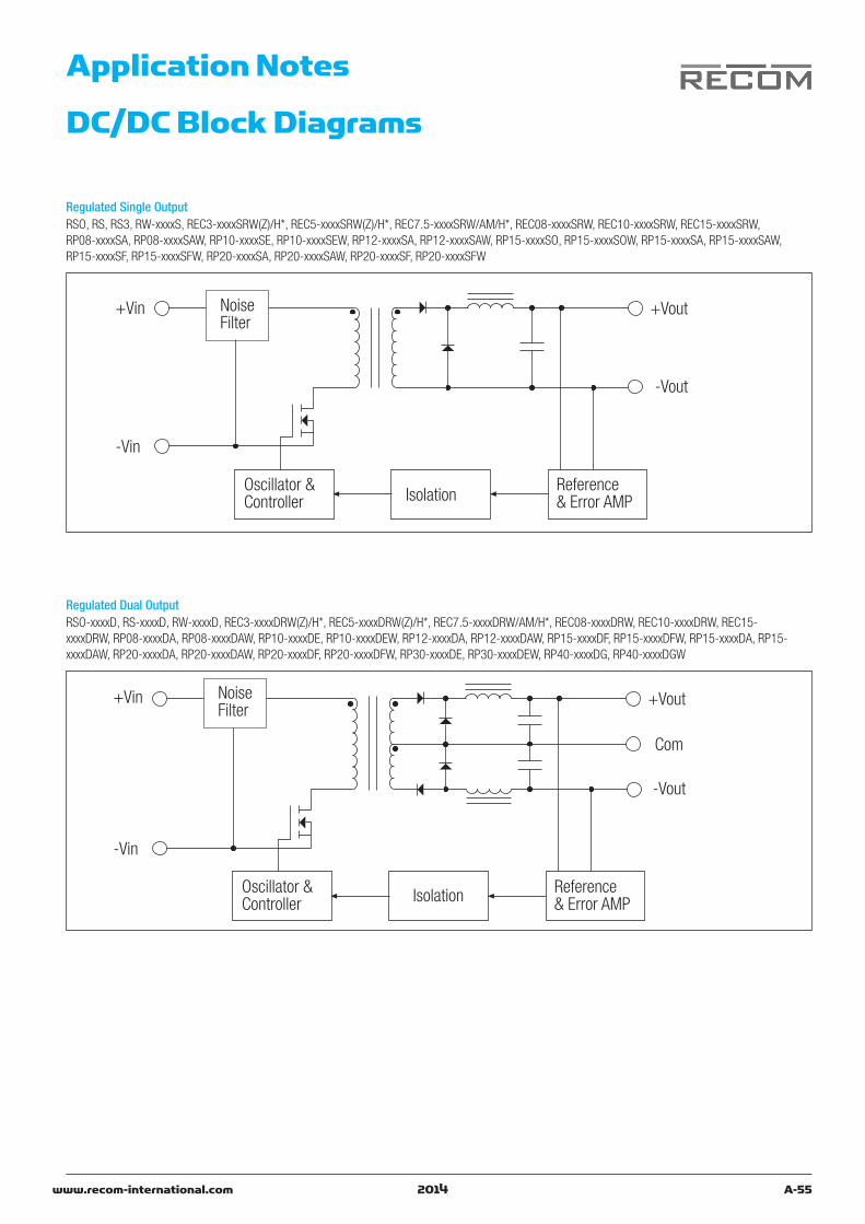
www.recom-international.com A-552014
Regulated Single Output RSO, RS, RS3, RW-xxxxS, REC3-xxxxSRW(Z)/H*, REC5-xxxxSRW(Z)/H*, REC7.5-xxxxSRW/AM/H*, REC08-xxxxSRW, REC10-xxxxSRW, REC15-xxxxSRW,RP08-xxxxSA, RP08-xxxxSAW, RP10-xxxxSE, RP10-xxxxSEW, RP12-xxxxSA, RP12-xxxxSAW, RP15-xxxxSO, RP15-xxxxSOW, RP15-xxxxSA, RP15-xxxxSAW,RP15-xxxxSF, RP15-xxxxSFW, RP20-xxxxSA, RP20-xxxxSAW, RP20-xxxxSF, RP20-xxxxSFW
����@����0
�����
��������� !�2�0����N��00�0�'A,
�����
����
����
���������0�N����0����0
Regulated Dual Output RSO-xxxxD, RS-xxxxD, RW-xxxxD, REC3-xxxxDRW(Z)/H*, REC5-xxxxDRW(Z)/H*, REC7.5-xxxxDRW/AM/H*, REC08-xxxxDRW, REC10-xxxxDRW, REC15-xxxxDRW, RP08-xxxxDA, RP08-xxxxDAW, RP10-xxxxDE, RP10-xxxxDEW, RP12-xxxxDA, RP12-xxxxDAW, RP15-xxxxDF, RP15-xxxxDFW, RP15-xxxxDA, RP15-xxxxDAW, RP20-xxxxDA, RP20-xxxxDAW, RP20-xxxxDF, RP20-xxxxDFW, RP30-xxxxDE, RP30-xxxxDEW, RP40-xxxxDG, RP40-xxxxDGW
����@����0
��;
�����
��������� !�2�0����N��00�0�'A,
�����
����
����
���������0�N����0����0
DC/DC Block Diagrams
Application Notes

A-56 www.recom-international.com2014
Regulated Single Output, Synchronous Rectification RP20-xxxxSF, RP20-xxxxSA, RP20-xxxxSAW, RP30-xxxxSE, RP30-xxxxSEW, RP40-xxxxSG, RP40-xxxxSGW, RP60-xxxxSG
"=���6����0��
��;
�$�@@����0��
�����
��������� !�2�0����N��00�0�'A,
/0�;
����
����
,#A����0����0
Regulated Triple OutputRP40-05xxTG
����@����0
������
��������� !�2�0����N��00�0�'A,
������
����
����
���������0�N����0����0
��;
����7
����7
DC/DC Block Diagrams
Application Notes
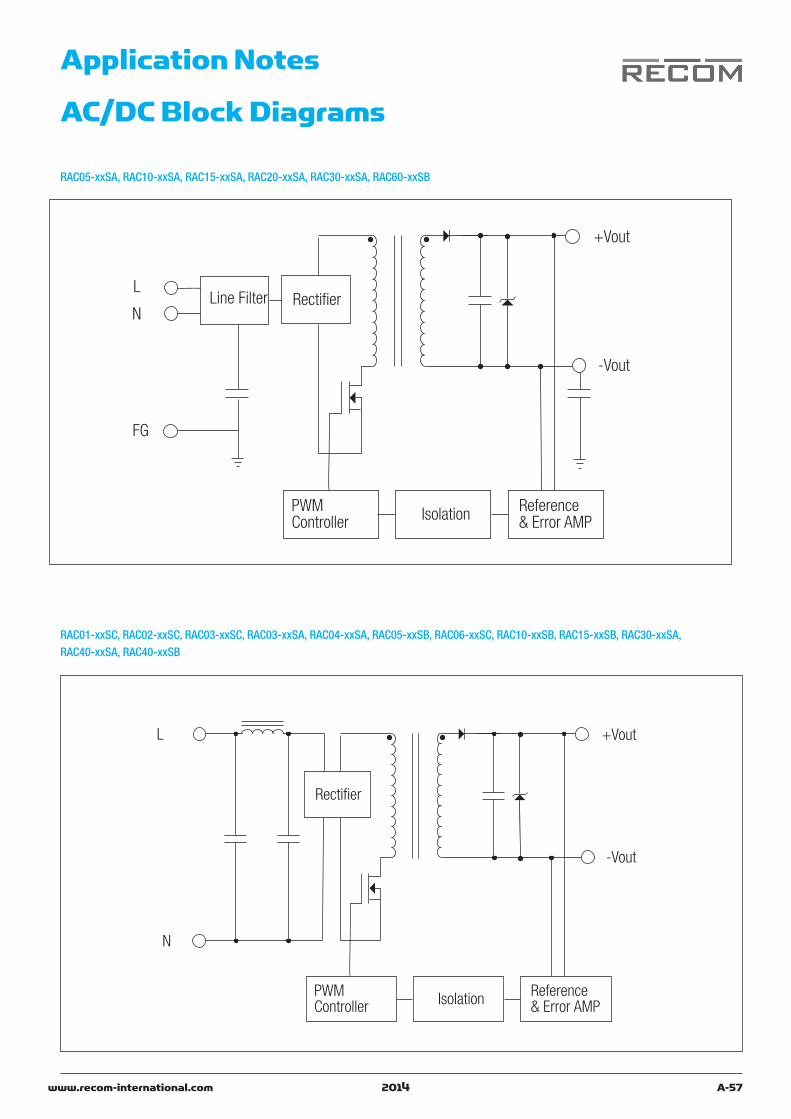
www.recom-international.com A-572014
!����2��0
@
�����@����0
�����
��������� !�2�0����N��00�0�'A,
�����
�
,#A����0����0
!����2��0
�����
��������� !�2�0����N��00�0�'A,
�����
�
,#A����0����0
RAC05-xxSA, RAC10-xxSA, RAC15-xxSA, RAC20-xxSA, RAC30-xxSA, RAC60-xxSB
RAC01-xxSC, RAC02-xxSC, RAC03-xxSC, RAC03-xxSA, RAC04-xxSA, RAC05-xxSB, RAC06-xxSC, RAC10-xxSB, RAC15-xxSB, RAC30-xxSA, RAC40-xxSA, RAC40-xxSB
AC/DC Block Diagrams
Application Notes

A-58 www.recom-international.com2014
!����2��0@����0
@
�5�0��00���,0��������
��;
�����
��������� !�2�0����N��00�0�'A,
�����
�
,#A����0����0
RAC05-xxDA, RAC10-xxDA, RAC15-xxDA, RAC20-xxDA, RAC30-xxDA
RAC06-xxDC, RAC15-xxDB, RAC30-xxDA, RAC40-xxDA, RAC40-xxDB
!����2��0@����0
�5�0��00���,0��������
�����
��������� !�2�0����N��00�0�'A,
�����
�
,#A����0����0
AC/DC Block Diagrams
Application Notes

www.recom-international.com A-592014
!����2��0
@
�����@����0
��������� !�2�0����N��00�0�'A,
�����
�
,#A����0����0
�����
��;
� ����
� ��!��
�5�0��00���,0��������
RAC15-05xxTA, RAC20-05xxTA
!����2��0�����@����0
��������� !�2�0����N��00�0�'A,
�����
�
,#A����0����0
�����
��;
� ����
� ��!��
�5�0��00���,0��������
RAC15-05xxTB, RAC30-05xxTA, RAC40-05xxTA
AC/DC Block Diagrams
Application Notes

A-60 www.recom-international.com2014
No. Types
1. RO, RM, RN, RNM, RE, ROM, RB, RBM, RK, RH, RP, RU, RI, RD, RKZ, RUZ, RY,R-78xx-0.5, R-78xx-1.0, R-78Cxx-1.0, R-78Exx-0.5, R-78Exx-1.0
2. RS, RSO, RS33. RJZ, RGZ, RW2(B)4. RSS, RSD, RZ, R1S, R1D, R1Z, R0.5Z5. RTD, RTS, RSZ, R-78Axx-xx SMD, R2S, R2D, R-78AAxx-xx SMD6. RV, RW-S, RxxPxx, RxxP2xx, RW2(A)-SMD7. R-5xxxPA, R-6xxxP, R-7xxxP, RW-D,
REC3-, REC3.5, REC5-, REC6-, REC7.5-8. RP08, RP12, REC8, REC10, RCD-24-xxx9. RP15-O, RP15-OW, RP15-A, RP15-AW, REC1510. RAC01, RAC0211. RP10, RP15, RP20, RP30, RP4012. RP08-SMD, REC3-SMD, REC5-SMD, REC7.5-SMD13. R-78Bxx-xx, R-78HBxx-xx14. R-78Bxx-xxL, R-78HBxx-xxL15. R-5xxxDA, R-6xxxD, R-7xxxD
all dimensions in mm
Transport Tubes
1. 2. 3.
TUBE LENGTH = 520±2.0 TUBE LENGTH = 520±1.5 TUBE LENGTH = 520±1.0

www.recom-international.com A-612014
7. 8.
Transport Tubes
4. 5. 6.
TUBE LENGTH = 530±2.0 TUBE LENGTH = 530±2.0 TUBE LENGTH =530±2.0
TUBE LENGTH = 530±2.0 TUBE LENGTH = 530±2.0
9.
TUBE LENGTH = 530±2.0 TUBE LENGTH = 520±1.0
10.
�.* ��*
��*9��*
)&*.��*
�9*-��*

A-62 www.recom-international.com2014
Transport Tubes
��*�����*
&*�����*
� *�����*
�*�����*�
�*�����*
9*�����*
/?�����/%���� -;;����*���*�����*
-*�����*
��*�����*
11.
12. 13.
�)*.����*�
-*)����*�
�*&)����*� +*)����*�
�.* ����*�
/?�����/%��� ��;;����*�
14.
�9*.��*�
��*���*�
�*9��*�
&* ��*�
+*���*�
/?�����/%��� ��;;����*�
��*�
)*)��*� ��*���*�
15.
�.*-���*�
��*)���*�
9*&����*�
�9*� ��*�
��*&.��*�
/?�����/%��� ��;;����*�
�*-���*�
�* ���*��9

www.recom-international.com A-632014
!""�. �7777�N�!�"�. �7777���1����������3�;�������
�)*�"1������6�����O�* ���*�$��"1������6��������0������5�0���4����1���6���M�*�
��*
�*9
�-*����M�*�
�*��
-*��
'���3�;�����������;;�77*77�M�*�
�*�����10������6����1���6���;�����5������0�����M�*��
�*�'���3�;��������;������'�-.����0�B��0�;����)*���;1���������3�1�0��)P�0����L� ���1��
-*�/6��3��;���0��2�3���������0�6��������)*�;;
�#�)?���-"-"
$$$$
�#�)?���-"-"
$$$$
�#�)?���-"-"
$$$$
��*-
�&*��
9*&
�*-����M�*�
Tape and Reel (Suffix -R)
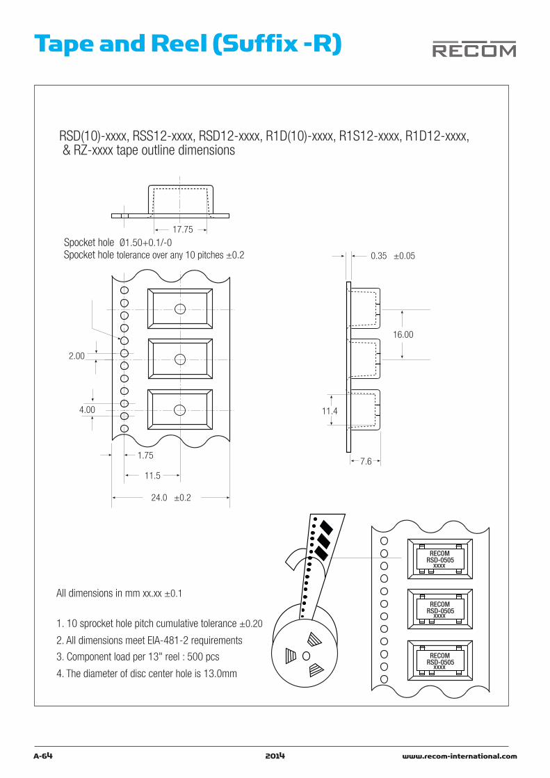
A-64 www.recom-international.com2014
Tape and Reel (Suffix -R)
!"���� �7777F�!""���7777F�!"����7777F�!����� �7777F�!�"���7777F�!�����7777F�N�!Q�7777���1����������3�;�������
�9*9 "1������6�����O�* ���*�$��"1������6��������0������5�0���4����1���6���M�*�
��*
�*9
�-*����M�*�
�*��
-*��
'���3�;�����������;;�77*77�M�*�
�*�����10������6����1���6���;�����5������0�����M�*��
�*�'���3�;��������;������'�-.����0�B��0�;����)*���;1���������3�1�0��)P�0����L� ���1��
-*�/6��3��;���0��2�3���������0�6��������)*�;;
�#�)?���-"-"
$$$$
�#�)?���-"-"
$$$$
�#�)?���-"-"
$$$$
��*-
�&*��
9*&
�*) ���M�*�

www.recom-international.com A-652014
Tape and Reel (Suffix -R)
!"Q�7777F�!/"�7777F�!�"�7777F�!/��7777F�!���7777!�9.'77�77"A��N�!�9.''77�77"A����1����������3�;�������
� * "1������6�����O�* ���*�$��"1������6��������0������5�0���4����1���6���M�*�
��*
�*9
�-*����M�*)
�*��
-*��
'���3�;�����������;;�77*77�M�*�
�*�����10������6����1���6���;�����5������0�����M�*��
�*�'���3�;��������;������'�-.����0�B��0�;����)*���;1���������3�1�0��)P�0����L� ���1��
-*�/6��3��;���0��2�3���������0�6��������)*�;;
�#�)?�@�-"-"
$$$$
�#�)?�@�-"-"
$$$$
�#�)?�@�-"-"
$$$$
��*
��*��
+*+
�* ���M�*�