Embed Size (px)
Citation preview

Freescale SemiconductorApplication Note
© Freescale Semiconductor, Inc., 2010. All rights reserved.
This application note provides the necessary information, considerations, and the procedure to add or adapt a new Liquid Crystal Display (LCD) panel to the Board Support Package (BSP) distribution for the i.MX31 PDK. The document describes the general LCD panel information and the generalities of the display controller module. It describes the development process to adapt a new LCD panel to the BSP, considering that the framework driver structure is already provided by the operating system. This application note assumes that the reader is familiar with the Microsoft® Platform Builder packages and the WinCE device driver concepts.
1 Overview of i.MX31 DisplaysAs a multimedia processor, the i.MX31 supports several types of displays.The display devices are handled by a special module called the image processing unit (IPU). This module also handles other graphic interfaces such as cameras and 2D graphics acceleration. All IPU sub-modules are connected by a private DMA interface (IDMA) used only for the IPU to transfer data between the sub-modules and also between the IPU and the external memory.
Document Number: AN4041Rev. 0, 03/2010
Contents1. Overview of i.MX31 Displays . . . . . . . . . . . . . . . . . . 12. LCD Principles . . . . . . . . . . . . . . . . . . . . . . . . . . . . . . 23. IPU-SDC Generalities . . . . . . . . . . . . . . . . . . . . . . . . . 54. Display Configuration in Windows CE 5.0 and 6.0 . 235. Summary and Tips . . . . . . . . . . . . . . . . . . . . . . . . . . 616. References . . . . . . . . . . . . . . . . . . . . . . . . . . . . . . . . . 657. Revision History . . . . . . . . . . . . . . . . . . . . . . . . . . . . 65
Different Display Configurations on the i.MX31 WinCE PDKby Multimedia Application Division
Freescale Semiconductor, Inc.Austin, TX

Different Display Configurations on the i.MX31 WinCE PDK, Rev. 0
2 Freescale Semiconductor
LCD Principles
Figure 1 shows a functional block diagram of IPU.
Figure 1. IPU Functional Block Diagram
The process of selecting an LCD for a mobile device involves several conflicts with respect to the requirements. Some of the conflicts are as follows:
• Large amounts of data, implying high rate of data transfer and processing, requiring significant resources
• Flexibility to support a variety of use cases
• Size, cost, and power consumption
Freescale provides reference designs for the i.MX family where the functionality of LCD is demonstrated. However, developers find many reasons to replace the display in their products. Features such as screen size, resolution, weight, power consumption, and price are important in a commercial multimedia product. Another important fact about LCD panels is that many displays quickly become obsolete and it is hard to find the same LCD panel included in the reference design when creating a product.
This application note is intended only for dumb displays and mainly those displays which do not have the sharp synchronous interface. However, some information in the application notes are also useful for smart displays.
NOTEDo not confuse sharp panels with sharp interface as there are a number of sharp panels which do not use the sharp interface.
2 LCD PrinciplesThe following sections explains the principles of LCD.
Different Display Configurations on the i.MX31 WinCE PDK, Rev. 0
Freescale Semiconductor 3
LCD Principles
2.1 LCD BasicsThe LCD is an electronic device which consists of an array of pixels which can be color or monochrome units. Every pixel in the array consists of a special material that allows the LCD to change the characteristics of the light that passes through them. These devices do not emit light and thus, another element named backlight is shipped with the panel to create a full functional device.
2.1.1 ResolutionIn this application note, the term resolution is used to refer to the number of pixels in an LCD array. It has two dimensions: horizontal and vertical. Table 1 lists the most common video resolution standards available in the market.
The maximum resolution that the i.MX31 supports is SVGA and hence, resolutions greater than SVGA are not included in the table above. All resolutions mentioned in Table 1 refer to a landscape orientation of LCD panels, which means that there are more horizontal pixels than vertical pixels. However, there are also portrait orientated LCD panels available in the market with the same standard resolution. These portrait LCD panels have more vertical pixels compared to horizontal pixels.
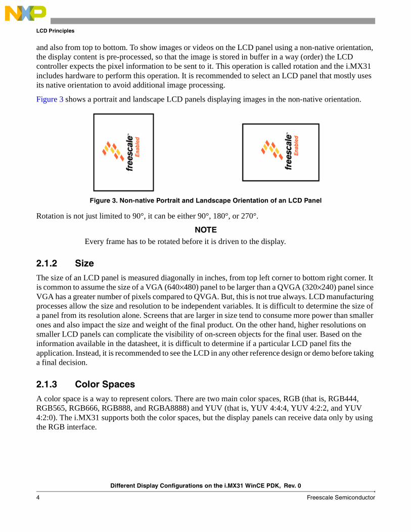
Figure 2 shows the portrait and landscape orientation of an LCD panel.
Figure 2. Portrait and Landscape Orientation of an LCD Panel
It is important to select the proper orientation of an LCD panel, because both the electronic and optical features are optimized for applications that use the native orientation of the panel. Besides the optical characteristics, the dumb displays include an embedded LCD controller to draw the pixels from left to right
Table 1. Common Video Resolution Standard s
Video Name Description Width Height Aspect Ratio
CGA Color Graphics Adapter 320 200 8:5
QVGA Quarter VGA 320 240 4:3
VGA Video Graphics Array 640 480 4:3
NTSC National Television System Committee 720 480 3:2
PAL Phase Alternating Line (TV) 720 576 5:4
WVGA Wide VGA 800 480 5:3
SVGA Super VGA 800 600 4:3
Different Display Configurations on the i.MX31 WinCE PDK, Rev. 0
4 Freescale Semiconductor
LCD Principles
and also from top to bottom. To show images or videos on the LCD panel using a non-native orientation, the display content is pre-processed, so that the image is stored in buffer in a way (order) the LCD controller expects the pixel information to be sent to it. This operation is called rotation and the i.MX31 includes hardware to perform this operation. It is recommended to select an LCD panel that mostly uses its native orientation to avoid additional image processing.
Figure 3 shows a portrait and landscape LCD panels displaying images in the non-native orientation.
Figure 3. Non-native Portrait and Landscape Orientation of an LCD Panel
Rotation is not just limited to 90°, it can be either 90°, 180°, or 270°.
NOTEEvery frame has to be rotated before it is driven to the display.
2.1.2 SizeThe size of an LCD panel is measured diagonally in inches, from top left corner to bottom right corner. It is common to assume the size of a VGA (640×480) panel to be larger than a QVGA (320×240) panel since VGA has a greater number of pixels compared to QVGA. But, this is not true always. LCD manufacturing processes allow the size and resolution to be independent variables. It is difficult to determine the size of a panel from its resolution alone. Screens that are larger in size tend to consume more power than smaller ones and also impact the size and weight of the final product. On the other hand, higher resolutions on smaller LCD panels can complicate the visibility of on-screen objects for the final user. Based on the information available in the datasheet, it is difficult to determine if a particular LCD panel fits the application. Instead, it is recommended to see the LCD in any other reference design or demo before taking a final decision.
2.1.3 Color SpacesA color space is a way to represent colors. There are two main color spaces, RGB (that is, RGB444, RGB565, RGB666, RGB888, and RGBA8888) and YUV (that is, YUV 4:4:4, YUV 4:2:2, and YUV 4:2:0). The i.MX31 supports both the color spaces, but the display panels can receive data only by using the RGB interface.

Different Display Configurations on the i.MX31 WinCE PDK, Rev. 0
Freescale Semiconductor 5
IPU-SDC Generalities
2.2 LCD TypesThe LCD panels are categorized as synchronous and asynchronous panels. The following sections discuss the types of LCD panels.
2.2.1 Synchronous Panel (Dumb Display)Dumb displays or synchronous displays are panels which require the microprocessor to send all pixels in the image of every frame. In these panels, screen refresh is performed by driving the complete frame data continuously. After drawing a pixel, the LCD waits for the next pixel data. In general, smart displays are more expensive than dumb displays, and this is the reason why synchronous panels are more commonly used in the final product. This application note focuses on thin film transistor (TFT) LCD panels which belong to a special group of synchronous panels.
2.2.2 Asynchronous Panel (Smart Display)The advantage of smart displays is that the i.MX31 only has to send display data when the image has changed, and most of the times send only the portion that has changed. Images can be sent at any time, the screen refresh is handled by the embedded Smart LCD display controller included in the LCD panel. Another advantage is that i.MX31 handles three asynchronous displays simultaneously and also handle the synchronous interface at the same time. In conclusion, if an application needs two LCD panels, one of them must be an asynchronous interface.
3 IPU-SDC GeneralitiesThe following sections discuss the IPU Synchronous Display Controller generalities.
3.1 LCD InterfacesThe following section explains the LCD interfaces with examples.
3.1.1 Synchronous Display InterfaceThe i.MX31 synchronous display controller is configured to handle four different types of devices such as TFT monochrome, TFT color, YUV progressive, and YUV interlaced, but this application note is only focused on the Synchronous TFT Color interface. The i.MX31 provides a 22-line interface which is described in Table 2.
.
Table 2. Synchronous Display Interface Signals
Signal IPU Signal Description
HSYNC DISPB_D3_HSYNC Horizontal synchronization
VSYNC DISPB_D3_VSYNC Vertical synchronization
DRDY DISPB_D3_DRDY Data enable or Data ready
PIXCLK DISPB_D3_CLK Pixel clock

Different Display Configurations on the i.MX31 WinCE PDK, Rev. 0
6 Freescale Semiconductor
IPU-SDC Generalities
The description of the signals referred in Table 2 are as follows:
HSYNC Horizontal synchronization (HSYNC) signal is also known as FPLINE or LP. This signal indicates the LCD that a line has ended and the following valid pixels are part of the next line.
VSYNC Vertical synchronization (VSYNC) signal is also known as FPFRAME, FLM, SPS, or TV. This signal when active indicates the LCD that the current frame has ended. The LCD display must then restart the line index to zero to draw the next valid data in the first line of the panel.
DRDY The data ready (DRDY) or data enable (DE) signal, when active, indicates the LCD that the data in the RGB bus is valid and must be latched using the PIXCLK signal. Every PIXCLK pulse indicates the LCD to draw a pixel using the color described in the RGB bus. The width of this signal must be enough to store all pixels (that is, as long as all pixel clock cycles of a single line).
PIXCLK The polarity of the pixel clock (PIXCLK) signal indicates, when the RGB data is placed on the bus. The following are the two different possibilities:
• The high polarity of PIXCLK indicates that data is written on the RGB bus on falling edges and data is latched by the LCD panel on rising edges. This is valid when DE is active.
• The low polarity of PIXCLK indicates that data is written on the RGB bus on rising edges and data is latched onto the LCD panel on falling edges. This is valid when DE is active.
RGB Data (Display Interface) The i.MX31 internally use different types of bits per pixel such as RGB565, RGB666, RGB888 and RGBA8888, and so on. The display interface is limited to18 lines and so, any image or video that contains pixels more than 18 bits (RGB666) cannot be sent to the display. During this RGB to RGB conversion least significant bits are removed from the pixel, and remaining bits are directly sent to the display interface. Any dithering or filter action is not performed during this process.
Extra Signals There are also some other signals that are usually included in the panel interface. These signals are not part of the 22-line display interface, but they are required for a full functional module. For example, it is common that some panels need a reset signal and also initialization commands. These commands are usually sent by a serial interface such as I2C or SPI.
Red Data[7:0] DISPB_DATA[17:12] Pixel Red component
Green Data[7:0] DISPB_DATA[11:6] Pixel Green component
Blue Data[7:0] DISPB_DATA[5:0] Pixel Blue component
Table 2. Synchronous Display Interface Signals (continued)
Signal IPU Signal Description

Different Display Configurations on the i.MX31 WinCE PDK, Rev. 0
Freescale Semiconductor 7
IPU-SDC Generalities
Display panels sometimes have backlight unit and touch panels embedded on them, which require additional signals.
SPI Interface Some LCD displays require an initialization routine through a serial interface, 3-wire, 4-wire, or 5-wire. A serial interface (SD_D_CLK, LCS1, SD_D_IO and SD_D_I) in i.MX31 IPU is not used to send serial commands to the LCDs. This interface is not intended for general purpose usage, it is used only by the IPU when the Asynchronous Display1 or Display2 are configured to use the serial interface.
3.1.1.1 Examples of Synchronous Display Interfaces
The following section provides few examples of the interface between the i.MX31 PDK and synchronous display panels.

Different Display Configurations on the i.MX31 WinCE PDK, Rev. 0
8 Freescale Semiconductor
IPU-SDC Generalities
i.MX31 PDK Epson L4F00242T03 2.7" VGA LCD Interface
Figure 4 shows the LCD interface between i.MX31 and Epson L4F00242T03 VGA panel.
Figure 4. Interface between i.MX31 and Epson L4F00242T03 VGA Panel
The LCD panel is shipped with the i.MX31 PDK as shown in Figure 4. The LCD panel requires HSYNC, VSYNC, DE, PIXCLK, and the complete RGB data interface (DISPB_DATA[17:0]). Additional signals such as a RESET signal and a serial interface are required for sending the initialization routine commands (SPI). The backlight unit is controlled by using a PWM signal generated by the i.MX31 (Contrast) and finally the touch panel interface is handled by the MC13783 Atlas chip.
Every panel has its own interface and requirements, but in general terms the example above illustrates a typical synchronous panel interface. It is difficult to determine what is typical LCD panels, and hence consider the possibility shown in Figure 4 as the base for the panel interface.
The idea of the base interface is useful when there are many panels which do not use the complete interface. For example, some of them do not require either HSYNC or VSYNC signals, or neither of them,

Different Display Configurations on the i.MX31 WinCE PDK, Rev. 0
Freescale Semiconductor 9
IPU-SDC Generalities
only DRDY, PIXCLK, and RGB data are used. Similarly, many others do not require a RESET or a serial initialization routine to handle display signals. The timing, signals, porches, and polarities are already specified when there is no serial interface. The panels expect that the microprocessors accomplish with these waveforms when these LCD panel cannot handle a different interface.
The only disadvantage is that this panel does not provide the backlight power booster, and it needs an external chip to amplify the contrast signal.
i.MX31 PDK Chunghwa CLAA070VC01 7" WVGA LCD Interface
Figure 5 shows the LCD interface between i.MX31 and Chunghwa CLAA070VC01VWGA panel.
Figure 5. Interface between i.MX31 and Chunghwa CLAA070VC01VWGA Panel
Figure 5 shows a simple display interface where HSYNC and VSYNC signals are not used. If the DISPB_D3_VSYNC and DISPB_D3_HSYNC pins are not used, the pins can be used for other purposes, such as a GPIO configuration. HSYNC can be used as SDMA_DEBUG_EVENT_CHANNEL_5 but VSYNC has no other functionality.
Also, SPI interface is not required so there is also a Chip Select (CSPI1_SS2) available for other devices. Additionally, the power booster for the backlight unit is included into the module and thus the CONTRAST signal is directly connected to the display connector.
NOTEThe display module does not include a touch panel and it is necessary to add an external touch screen to this LCD panel.
It is important to remember that, since these LCD modules neither have RESET signal nor a SPI interface, the display cannot be turned off. This feature is important for mobile devices where power consumption is into consideration. So to control the energy in the LCD, the external circuits must be controlled.

Different Display Configurations on the i.MX31 WinCE PDK, Rev. 0
10 Freescale Semiconductor
IPU-SDC Generalities
Based on the above observations, the complete system is as shown in Figure 6.
Figure 6. Interface between i.MX31 and Chunghwa CLAA070VC01VWGA Panel + Touch Panel
The above examples help the user to select an LCD and also to determine the advantages and disadvantages of any panel.
3.1.2 Synchronous Display Timing and SignalsThis section focusses on the timing and signal waveforms and how to configure them in the LCD panel and i.MX31 display interface. The first step to select an LCD module is to refer its datasheet. The datasheet must describe the pin interface, the initialization routine, the timing charts for RGB interface and, serial interface. Many times a shorter version of the datasheet available does not contain all this information. In this case, it is advisable to request the full documentation from the supplier. Many times the datasheet that are available is a preliminary datasheet. Though there is not much difference between preliminary and final versions, it is always better to have the final version, especially in LCD datasheets.
3.1.2.1 Timing Concepts
This section explains certain important concepts and considerations which form the base for timing in an LCD interface.
Horizontal Back porch (HBP) Number of pixel clock pulses between the beginning of HSYNC signal and the first valid pixel data.

Different Display Configurations on the i.MX31 WinCE PDK, Rev. 0
Freescale Semiconductor 11
IPU-SDC Generalities
Horizontal Front Porch (HFP) Number of pixel clock pulses between the last valid pixel data in the line and the next HSYNC pulse.
Vertical Back Porch (VBP) Number of lines (HSYNC pulses) between the beginning of VSYNC signal and the first valid line.
Vertical Front Porch (VFP) Number of lines (HSYNC pulses) between the last valid line of the frame and the next VSYNC pulse.
VSYNC Pulse Width Number of HSYNC pulses during which the VSYNC signal is active.
HSYNC Pulse Width Number of pixel clock pulses during which the HSYNC signal is active.
Active Frame Width This value is basically the horizontal resolution or the number of pixels in one line. For example, for a WVGA display (800H×480V), the value of active frame width is equal to 800 pixels.
Active Frame Height This value is equal to the vertical resolution of the LCD. For example, for a WVGA display (800H×480V), the value of frame height is equal to 480 pixels.
Screen Width This is misleading as screen width does not denote the horizontal resolution of the LCD panel (number of pixels in one line). For the i.MX31, the SCREEN_WIDTH is the number of pixel clock periods between the last HSYNC and the new HSYNC. So, this value includes the valid pixels and also the horizontal back and front porches.
SCREEN_WIDTH = ACTIVE_FRAME_WIDTH + HBP + HFP Eqn. 1
Screen Height For the i.MX31, the SCREEN_HEIGHT is the number of rows between the last VSYNC pulse and the new VSYNC pulse. It includes all valid lines and also the vertical back and front porch.
SCREEN_HEIGHT = ACTIVE_FRAME_HEIGHT + VBP + VFP Eqn. 2
VSYNC Polarity It is the value of VSYNC which indicates the starting of a new frame. It is active low when the value is 0 or active high when it is 1.
HSYNC Polarity It is the value of HSYNC which indicates the starting of a new line. It is active low when the value is 0 or active high when it is 1.
3.1.2.2 Timing Charts
To understand the timing issues in a LCD interface, review the following charts in the datasheet:
• Vertical timing characteristics
• Horizontal timing characteristics
• Pixel clock characteristics
Additionally, if the display uses a serial interface, refer to another chart describing the serial interface and the RESET. This is the information that must be extracted from the datasheet when a support for a new LCD panel is added.

Different Display Configurations on the i.MX31 WinCE PDK, Rev. 0
12 Freescale Semiconductor
IPU-SDC Generalities
Consider a VGA (640H×480V) LCD panel using the same interface than EPSON L4F00242T03, see Figure 4. The display uses the RGB666, VSYNC, HSYNC, data enable, and pixel clock. It also requires a RESET signal and a serial interface.
Vertical Timing
The following sections describe the VGA and WVGA vertical timing characteristics.
VGA Vertical Timing
Figure 7 shows the vertical timing for a hypothetical synchronous display VGA (480H×640V).
Figure 7. VGA Vertical Timing Example
It is important to mention how signals appear during the VSYNC period. VSYNC period involves a complete frame cycle; every pixel and every line in the frame is sent to the panel during this cycle. The beginning of the frame is set by the VSYNC signal, in this case when signal goes low. Then HSYNC immediately marks the beginning of the first line, in this example it is when HSYNC goes low. To meet the LCD timing requirements, the first lines are designated for the VBP. During VBP, data enable signal is not present and the pixel data on the bus is ignored by the panel. After VBP, data enable signal appears inside the boundaries of the HSYNC period. The details about DE during a line cycle are reviewed in the next section. DE appears consequently during all valid lines (Vertical resolution = 640V). During this time (Active frame height) the LCD panel latches the RGB data on all lines and draws it on the screen. The final stage in the frame cycle is the VFP, where extra lines (HSYNC cycles) appear. During this time, DE

Different Display Configurations on the i.MX31 WinCE PDK, Rev. 0
Freescale Semiconductor 13
IPU-SDC Generalities
remains inactive and again the panel discards any information on the RGB bus. The frame ends when VSYNC signal is set again (goes low).
Table 3 shows the range of the timing parameters shown in Figure 7.
From the information described above, verify some of the timing features. In the first waveform, it is shown that VSYNC polarity is active low, which means that vertical synchronization is normally high, but goes low to indicate the beginning of the new frame. Another feature is the VSYNC width (VSW). Timing has certain flexibility and more than one value is used to set the timing. It is highly recommended to use the typical values or any values close to them. Here, consider 10 lines as VSYNC width.
Vertical back porch (VBP) and vertical front porch (VFP) are shown too; notice that these values are measured in lines or which translates into HSYNC pulses. In this example, VBP is 10 lines, and VFP is of 5 lines width. VSYNC width is included into the VBP stage. This means that VBP starts when VSYNC is set, and not when the VSYNC returns to normal state. Using the values described in, the value of screen height or vertical cycle is 665. In some cases, the value of the VBP and VFP is not given in lines; instead it is expressed in nanoseconds or milliseconds. In this case, an additional calculation is performed to find the number of lines needed to meet those timings.
Table 3. VGA Vertical Timing
Parameter Symbol Min Typ Max Unit
Screen height or Vertical period VP — 665 — Line
VSYNC pulse width VSW 5 10 15 Line
Vertical back porch VBP 5 10 15 Line
Vertical front porch VFP 5 5 5 Line
Active frame height VDISP — 640 — Line
Vertical refresh rate FV — 60 — Hz

Different Display Configurations on the i.MX31 WinCE PDK, Rev. 0
14 Freescale Semiconductor
IPU-SDC Generalities
WVGA Vertical Timing
If an LCD panel like the hypothetical WVGA (800H X 480V) are used as described in Figure 5 and Figure 6, which does not use HSYNC and VSYNC signals, the waveforms are analyzed in another perspective as shown in Figure 8.
Figure 8. WVGA Vertical Timing Example
Table 4 shows the range of the timing parameters shown in Figure 8.
In these cases, VSYNC width, VSYNC polarity, vertical back porch and vertical front porch are not shown in the chart. Even when VSYNC is not used, these values are required for configuring the i.MX31 display interface. These waveforms are used to understand the vertical cycle behavior. For the i.MX31, the sequence remains the same; vertical cycle starts with the VSYNC signal, then the rest of the VBP, the active frame area, and finally the VFP appears until the next VSYNC is set. The trick to find the VSYNC width, VBP and VFP is based on the fact that those events happen during the Vertical Blank Period.
Table 4. WVGA Vertical Timing
Parameter Symbol Min Typ Max Unit
Screen height or Vertical period VP 490 500 520 Line
Vertical blank VBK 10 20 40 Line
Active frame height VDISP 480 480 480 Line
Vertical refresh rate FV 55 60 65 Hz

Different Display Configurations on the i.MX31 WinCE PDK, Rev. 0
Freescale Semiconductor 15
IPU-SDC Generalities
Figure 9 shows the WVGA vertical timing example with imaginary VSYNC signal.
Figure 9. WVGA Vertical Timing Example with Imaginary VSYNC Signal
The VSYNC signal is used only as a base to calculate vertical front porch and vertical back porch. When VSYNC is not used, it can be operated with any polarity. However, it is recommended to use VSYNC as an active low signal. VSYNC is usually one line long and thus the value of VSW is 1. To determine the values of VBP and VFP, divide the VBK period into two parts; the first part being the VFP before VSYNC and the second part for the VBP after VSYNC, and the sum of these values are equal to VBK period. It is recommended to have an imaginary VSYNC in the middle of VBK, so that the VBP and VFP must be equal or almost equal.
For example, if VBK is 20 lines (typical), the value of VBP is 10 lines which is equal to VFP. Based on the information described above, a vertical timing table such as Table 5 can be created.
Table 5. WVGA Vertical Timing and Porches
Parameter Symbol Min Typ Max Unit
Screen Height or Vertical cycle VP 490 500 520 Line
VSYNC pulse width VSW 1 1 1 Line
Vertical back porch VBP 1 10 40 Line
Vertical front porch VFP 0 10 39 Line
Vertical blank VBK 10 20 40 Line
Active frame height VDISP 480 480 480 Line
Vertical refresh rate FV 55 60 65 Hz

Different Display Configurations on the i.MX31 WinCE PDK, Rev. 0
16 Freescale Semiconductor
IPU-SDC Generalities
Horizontal Timing
The following sections describe the VGA and WVGA horizontal timing characteristics.
VGA Horizontal Timing
The datasheet also includes another chart which describes the line period, apart from the charts discussed earlier.
Figure 10 shows the horizontal timing for a hypothetical synchronous display VGA (640H×480V).
Figure 10. VGA Horizontal Timing Example
The line cycle begins when the HYSNC signal is set, in this case when the signal goes low. This is followed by the horizontal back porch stage. During this stage, the data enable signal is inactive. When the data enable signal is set, the next stage, which is the horizontal back porch, begins. The horizontal active area (ACTIVE FRAME WIDTH) begins, when data enable is set and when DE signal goes high. In this stage, the panel latches the RGB data on the bus and draws a new pixel on the screen for every pixel clock pulse. The width of the data enable signal is always equal to the horizontal resolution of the panel. For this example, the width of DE is 480 pixels. Once all the pixels in the line are drawn, DE is inactive again and the horizontal front porch begins. The line cycle ends when HYSNC pulse is set again.

Different Display Configurations on the i.MX31 WinCE PDK, Rev. 0
Freescale Semiconductor 17
IPU-SDC Generalities
Similar to the vertical timing characteristics, a table for the horizontal timing characteristics is shown in Table 6.
WVGA Horizontal Timing
The chart and table that are found in the datasheet is similar to the WVGA (800 H×480 V) example shown in Figure 11 and Table 7 respectively.
Figure 11. WVGA Horizontal Timing Example
The values of HBP, HFP and the HSYNC width are calculated using the same procedure used in the Section , “WVGA Vertical Timing”.
Table 6. VGA Horizontal Timing
Parameter Symbol Min Typ Max Unit
Screen width or Horizontal cycle HP 495 601 741 PIXCLK
HSYNC pulse width HSW 5 20 75 PIXCLK
Horizontal back porch HBP 5 60 75 PIXCLK
Horizontal front porch HFP 5 41 111 PIXCLK
Active frame width HDISP — 480 — PIXCLK
Table 7. WVGA Horizontal Timing
Parameter Symbol Min Typ Max Unit
Screen width or Horizontal cycle HP 850 900 950 PIXCLK
Horizontal blank period HBK 50 100 150 PIXCLK
Active frame width HDISP 800 800 800 PIXCLK
Different Display Configurations on the i.MX31 WinCE PDK, Rev. 0
18 Freescale Semiconductor
IPU-SDC Generalities
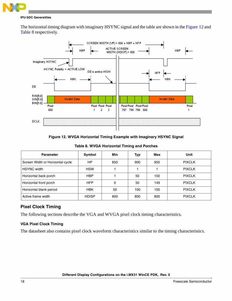
The horizontal timing diagram with imaginary HSYNC signal and the table are shown in the Figure 12 and Table 8 respectively.
Figure 12. WVGA Horizontal Timing Example with Imaginary HSYNC Signal
Pixel Clock Timing
The following sections describe the VGA and WVGA pixel clock timing characteristics.
VGA Pixel Clock Timing
The datasheet also contains pixel clock waveform characteristics similar to the timing characteristics.
Table 8. WVGA Horizontal Timing and Porches
Parameter Symbol Min Typ Max Unit
Screen Width or Horizontal cycle HP 850 900 950 PIXCLK
HSYNC width HSW 1 1 1 PIXCLK
Horizontal back porch HBP 1 50 150 PIXCLK
Horizontal front porch HFP 0 50 149 PIXCLK
Horizontal blank period HBK 50 100 150 PIXCLK
Active frame width HDISP 800 800 800 PIXCLK

Different Display Configurations on the i.MX31 WinCE PDK, Rev. 0
Freescale Semiconductor 19
IPU-SDC Generalities
The waveform characteristics chart and the table for a VGA pixel clock are as shown in the Figure 13 and Table 9 respectively.
Figure 13. VGA Pixel Clock Timing Example
The important feature regarding the pixel clock is to know when RGB data is latched by the panel, besides its relation with the frame refresh rate. This characteristic is very important because i.MX31 must prepare the data before LCD latches the data. A similar chart is included in the datasheet. In this example, data is latched by the LCD panel on DCLK rising edges, and thus the i.MX31 is configured to write the RGB data on the bus on the falling edge. In this manner the data will be ready and stable when the panel reads it. This waveform shows the typical inverse clock polarity. Clock polarity is set in DI_DISP_SIG_POL i.MX31 register under the D3_CLK_POL bit-field. The maximum and minimum values for the pixel clock frequency are not described in the table because only typical value is allowed.
The maximum display clock rate can not be greater than quarter of the high speed processing clock rate. HSP_CLK in the i.MX31 PDK BSP is 133 MHz, so the maximum pixel clock is 133 MHz/4= 33.25 MHz. However, most LCD displays work at lower frequencies than the typical values.
Table 9. VGA Pixel Clock Timing
Parameter Symbol Min Typ Max Unit
Pixel clock frequency PCLK — 24 — MHz
Different Display Configurations on the i.MX31 WinCE PDK, Rev. 0
20 Freescale Semiconductor
IPU-SDC Generalities
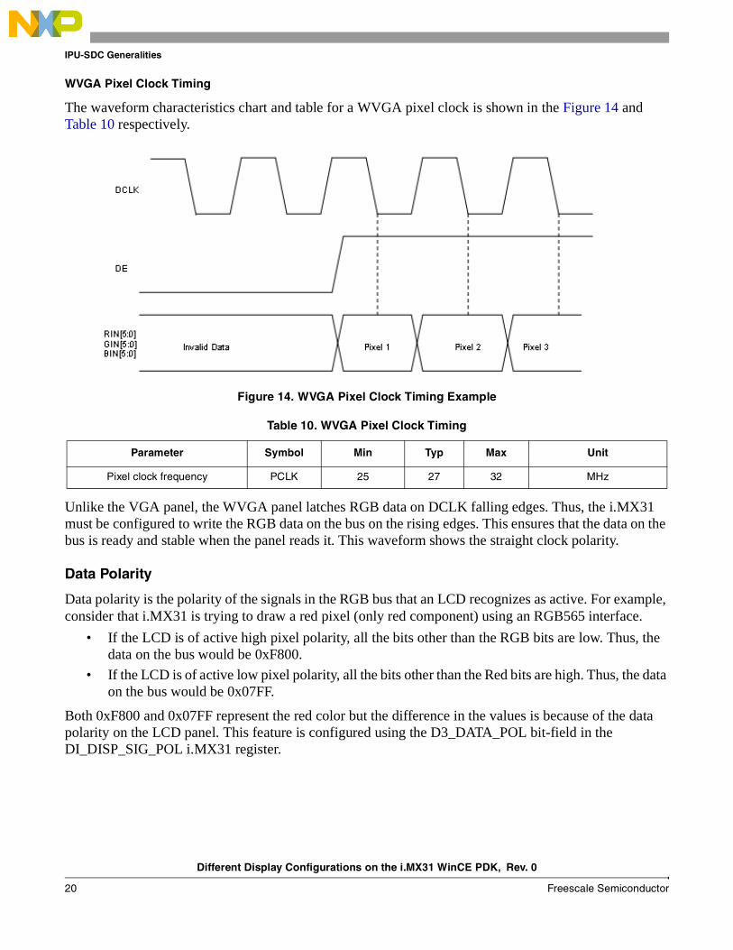
WVGA Pixel Clock Timing
The waveform characteristics chart and table for a WVGA pixel clock is shown in the Figure 14 and Table 10 respectively.
Figure 14. WVGA Pixel Clock Timing Example
Unlike the VGA panel, the WVGA panel latches RGB data on DCLK falling edges. Thus, the i.MX31 must be configured to write the RGB data on the bus on the rising edges. This ensures that the data on the bus is ready and stable when the panel reads it. This waveform shows the straight clock polarity.
Data Polarity
Data polarity is the polarity of the signals in the RGB bus that an LCD recognizes as active. For example, consider that i.MX31 is trying to draw a red pixel (only red component) using an RGB565 interface.
• If the LCD is of active high pixel polarity, all the bits other than the RGB bits are low. Thus, the data on the bus would be 0xF800.
• If the LCD is of active low pixel polarity, all the bits other than the Red bits are high. Thus, the data on the bus would be 0x07FF.
Both 0xF800 and 0x07FF represent the red color but the difference in the values is because of the data polarity on the LCD panel. This feature is configured using the D3_DATA_POL bit-field in the DI_DISP_SIG_POL i.MX31 register.
Table 10. WVGA Pixel Clock Timing
Parameter Symbol Min Typ Max Unit
Pixel clock frequency PCLK 25 27 32 MHz
Different Display Configurations on the i.MX31 WinCE PDK, Rev. 0
Freescale Semiconductor 21
IPU-SDC Generalities
3.1.2.3 Custom LCD Timing
Neither of the examples in this application note needs extra signals for LCD functionality. But if the LCD requires a reset signal or initialization routine through a synchronous serial interface, refer to charts similar to the following charts.
3.1.2.4 VGA Custom LCD Timing
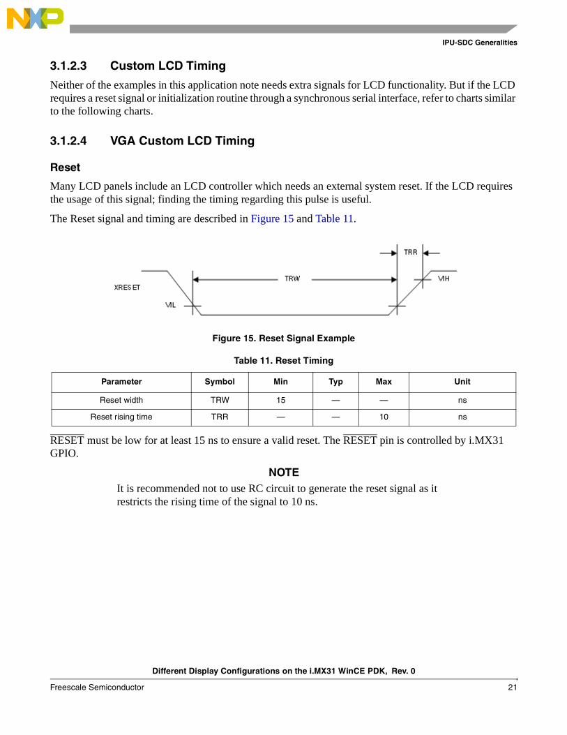
Reset
Many LCD panels include an LCD controller which needs an external system reset. If the LCD requires the usage of this signal; finding the timing regarding this pulse is useful.
The Reset signal and timing are described in Figure 15 and Table 11.
Figure 15. Reset Signal Example
RESET must be low for at least 15 ns to ensure a valid reset. The RESET pin is controlled by i.MX31 GPIO.
NOTEIt is recommended not to use RC circuit to generate the reset signal as it restricts the rising time of the signal to 10 ns.
Table 11. Reset Timing
Parameter Symbol Min Typ Max Unit
Reset width TRW 15 — — ns
Reset rising time TRR — — 10 ns

Different Display Configurations on the i.MX31 WinCE PDK, Rev. 0
22 Freescale Semiconductor
IPU-SDC Generalities
Serial command Interface
If the LCD panel has a serial command interface, the datasheet also contains a chart as shown in Figure 16.
Figure 16. SPI Command Interface Signals Example
This application note does not review all the serial interfaces that an LCD has. The protocols and data formats are described in the datasheet and it is important to have knowledge of synchronous serial interfaces to configure these settings. For more information, see Chapter 24, Configurable Serial Peripheral Interface (CSPI) of the MCIMX31 and MCIMX31L Applications Processors Reference Manual.
3.1.2.5 WVGA Custom LCD Timing
There are no custom signals regarding panel interface, since the WVGA panel does not need any reset or initialization.
3.2 LCD Panels Supported by the i.MX31The i.MX31 can handle up to four displays at the same time. Table 12 lists the various types of displays that are handled by display controllers.
Only one of the LCD display controllers in the i.MX31 is synchronous (dumb display), and thus this application note focusses on the DISP3 controller. The DISP3 RGB interface is multiplexed with all other asynchronous parallel interfaces, and so data cannot be sent to a synchronous display (DISP3) and another parallel device at the same time. Instead the i.MX31 sends data to the asynchronous panel (smart display)
Table 12. Displays Supported by the i.MX31
Display Controller Display Type Interface
DISP0 Asynchronous Parallel interface only
DISP1 Asynchronous Serial and Parallel interface
DISP2 Asynchronous Serial and Parallel interface
DISP3 Synchronous RGB Interface (HSYNC, VSYNC, PIXCLK, up to RGB666)

Different Display Configurations on the i.MX31 WinCE PDK, Rev. 0
Freescale Semiconductor 23
Display Configuration in Windows CE 5.0 and 6.0
when synchronous interface is inactive, and hence the frame rate in smart displays is affected when multiple displays are attached to the i.MX31.
The synchronous LCD interface in the i.MX31 is very flexible, and it handles many types of LCD devices with the following characteristics:
• Synchronous display (Dumb display)
• RGB interface (RGB666 maximum)
• Resolution not larger than SVGA
• Utilize at least data enable and pixel clock to latch RGB data (some LCD panels need HSYNC and VSYNC signals as well, which are also supported by the i.MX31)
• Pixel clock frequency lower than 33.25 MHz
In addition, the i.MX31 also handles dumb displays with a sharp interface, but its support is limited to certain models. For more information regarding the timing restrictions, refer the i.MX31 and i.MX31L Multimedia Applications Processors datasheet in section 4.3.15.3 Interface to Sharp HR-TFT Panels. Since this application note is only intended for non-sharp dumb displays, smart displays and sharp displays interfaces are not included in this reading.
4 Display Configuration in Windows CE 5.0 and 6.0LCD support is one of the most important features for any multimedia device. Display support enables the device to have a graphical user interface and the possibility of becoming an entertainment artifact.
The graphic context is composed of several layers, where the i.MX31 display interface is the final part in the abstraction. All the SDC and display interface characteristics that were reviewed in previous sections describes only the way the i.MX31 sends the frame buffer to the panel. However, it is important to know who is going to create the frames that need to be sent to the panel. If the screen is refreshed at 60 times per second (60 Hz), every line and every single pixel has to be created to maintain the coherence of the graphic context.
The i.MX31 PDK BSP bases its display driver on the Display Driver Interface (DDI) defined by Microsoft for all WINCE500 devices. Implementing a driver using this model ensures the compatibility of the hardware with the operating system. In other words, once WinCE is loaded and if the driver was created using the MS model, the OS handles the graphic context, providing all frames.
4.1 WinCE Display Driver Development ConceptsDisplay drivers are loaded and called directly by the graphics, windowing, and event subsystem, called Gwes.exe. Drivers are most commonly written using a layered architecture because of the number of hardware-independent operations.
The Graphics Primitive Engine (GPE) library handles the default drawing, acting as the display driver's model device driver (MDD) upper layer.
The user develops the hardware-specific code that corresponds to the display driver's lower layer, called the platform-dependent driver (PDD).

Different Display Configurations on the i.MX31 WinCE PDK, Rev. 0
24 Freescale Semiconductor
Display Configuration in Windows CE 5.0 and 6.0
Table 13 shows the elements that constitute the Windows CE graphics pipeline.
Figure 17 shows the Windows CE graphics architecture.
Figure 17. Windows CE Graphics Architecture
More details can be found under Display Drivers (Developing a Device Driver > Windows CE Drivers > Display Drivers) topic of Platform Builder for Microsoft Windows CE 5.0 help.
Table 13. Elements of Windows CE Graphics Pipeline
Element Description
Application The application can be simple, such as a Hello World application, or complex, such as a three-dimensional engineering application. Whichever it is, the application calls GDI functions. Coredll.dll exposes these functions.
Coredll.dll The major set of functions is exposed through a single DLL, called Coredll.dll.In most cases, this library does not perform the work. Instead, the library packages the parameters for the function call and then triggers a Local Procedure Call (LPC) to another process.The specific process depends on the function call. All drawing and windowing calls are sent to Gwes.exe.
Gwes.exe The Graphics, Windowing and Events Subsystem (GWES) is responsible for all graphical output and all interactions with the user. The drivers that reside in the GWES address space include display drivers, printer drivers, keyboard drivers, mouse drivers, and touch screen drivers.
Ddi.dll The default name for the display driver is Ddi.dll. As with most DLLs, Ddi.dll communicates through exported functions.Ddi.dll exports only the DrvEnableDriver function, which returns a pointer to an array of 27 function pointers to the caller. When GWES requires a display driver, it calls one of these 27 functions.Writing a device driver involves writing the code for these 27 functions. Three of these functions are specific to printer drivers, which leaves 24 for the display driver developer.
Hardware The graphic pipeline ends at the hardware. The display driver communicates to the hardware using the mechanism required by the hardware. This process typically involves a combination of memory-mapped video buffers and I/O registers.

Different Display Configurations on the i.MX31 WinCE PDK, Rev. 0
Freescale Semiconductor 25
Display Configuration in Windows CE 5.0 and 6.0
It is important to mention that develop a WinCE Display driver from scratch implicates a considerable effort and knowledge, specially regarding to the WinCE architecture. Fortunately Freescale provides the i.MX31 Display Driver for Synchronous Displays in the WINCE500 BSP. The i.MX31 Windows CE 5.0 BSP display driver is based on the Microsoft DirectDraw Graphics Primitive Engine (DDGPE) classes and supports the Microsoft DirectDraw interface. This driver combines the functionality of a standard LCD display with DirectDraw support. The display driver interfaces with the Image Processing Unit (IPU).This driver supports more than one panel which could be selected by using the Windows Register. You could easily add the support for a new SDC panel using the procedure described in this section.
4.2 Adding Support for a New LCD PanelThe following sections describes the procedure used to add the support for a new synchronous panel.
4.2.1 Identifying LCD Characteristics and TimingTo add the support for a new synchronous LCD display for the Freescale i.MX31 BSP, ensure that this panel is compatible with the i.MX31. The panel must have the following interface characteristics:
• Synchronous display (Dumb Display)
• RGB interface (RGB666 maximum)
• Resolution not bigger than SVGA
• Utilize at least data enable and pixel clock to latch RGB data (some LCD's need HSYNC and VSYNC signals which are also supported by the i.MX31).
• Pixel clock frequency lower than 33.25 MHz
Once a compatible LCD panel is selected, it is important to find the timing characteristics of the display interface and it is used to note the timing parameters. Table 14 and Table 15 can be used to note the timing parameters.
Table 14. LCD Timing Features
Parameter Symbol Min Typ Max Unit
Screen height or Vertical cycle VP — — — Line
Active frame height VDISP — — — Line
VSYNC pulse width VSW — — — Line
Vertical back porch VBP — — — Line
Vertical front porch VFP — — — Line
Vertical refresh rate FV — — — Hz
Screen width or Horizontal cycle HP — — — PIXCLK
Active frame width HDISP — — — PIXCLK
HSYNC pulse width HSW — — — PIXCLK
Horizontal back Porch HBP — — — PIXCLK
Different Display Configurations on the i.MX31 WinCE PDK, Rev. 0
26 Freescale Semiconductor
Display Configuration in Windows CE 5.0 and 6.0
More details on how to deduce these values from the LCD datasheet can be found prior in this document in sections 1 to 3.
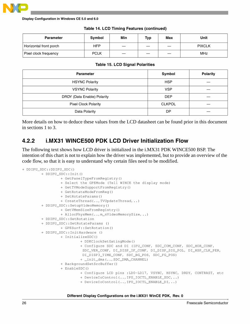
4.2.2 i.MX31 WINCE500 PDK LCD Driver Initialization FlowThe following text shows how LCD driver is initialized in the i.MX31 PDK WINCE500 BSP. The intention of this chart is not to explain how the driver was implemented, but to provide an overview of the code flow, so that it is easy to understand why certain files need to be modified.
+ DDIPU_SDC::DDIPU_SDC()+ DDIPU_SDC::Init()
+ GetPanelTypeFromRegistry()+ Select the GPEMode (Tell WINCE the display mode)+ GetTVModeSupportFromRegistry()+ GetRotateModeFromReg()+ SetRotateParams()+ CreateThread(..,TVUpdateThread,..)
+ DDIPU_SDC::SetupVideoMemory()+ GetVMemSizeFromRegistry()+ AllocPhysMem(..,m_nVideoMemorySize,..)
+ DDIPU_SDC::SetRotation+ DDIPU_SDC::SetRotateParams ()
+ GPESurf::SetRotation()+ DDIPU_SDC::InitHardware ()
+ InitializeSDC()+ DDKClockSetGatingMode()+ Configure SDC and DI (IPU_CONF, SDC_COM_CONF, SDC_HOR_CONF, SDC_VER_CONF, DI_DISP_IF_CONF, DI_DISP_SIG_POL, DI_HSP_CLK_PER, DI_DISP3_TIME_CONF, SDC_BG_POS, SDC_FG_POS)+ _init_dma(..,SDC_DMA_CHANNEL)
+ BackgroundSetSrcBuffer()+ EnableSDC()
+ Configure LCD pins :LD0-LD17, VSYNC, HSYNC, DRDY, CONTRAST, etc+ DeviceIoControl(..,IPU_IOCTL_ENABLE_SDC,..)+ DeviceIoControl(..,IPU_IOCTL_ENABLE_DI,..)
Horizontal front porch HFP — — — PIXCLK
Pixel clock frequency PCLK — — — MHz
Table 15. LCD Signal Polarities
Parameter Symbol Polarity
HSYNC Polarity HSP —
VSYNC Polarity VSP —
DRDY (Data Enable) Polarity DEP —
Pixel Clock Polarity CLKPOL —
Data Polarity DP —
Table 14. LCD Timing Features (continued)
Parameter Symbol Min Typ Max Unit
Different Display Configurations on the i.MX31 WinCE PDK, Rev. 0
Freescale Semiconductor 27
Display Configuration in Windows CE 5.0 and 6.0
+ BSPInitializeLCD()+ Configure CSPI pins+ Configure Reset Pin
+ BSPEnableLCD()+ DisplayOn()
+ PmicVoltageRegulatorOn(VMMC1)+ PmicVoltageRegulatorOn(VGEN)+ PmicVoltageRegulatorSetVoltageLevel(VMMC1,..)+ PmicVoltageRegulatorSetVoltageLevel(VGEN,..)+ Reset the Module+ Config CSPI registers+ LCD_CSPI_Write() - SPI LCD Initialization
+ DDIPU_SDC::AdvertisePowerInterface()
The DDIPU_SDC::DDIPU_SDC() function triggers the initialization of the LCD display driver. In a very high perspective, the driver reads the video memory size, rotation and panel type from the registry (platform.reg). Based on the selected panel, the driver notifies the WinCE display properties such as width, height, bits per pixel and so on (GPEMode). GPEMode data is extracted from the static GPEMode ModeArray[] in ddipu_sdc.cpp file. With this information, WinCE graphic context creates the frame buffers in the width, height and format required by the LCD, which is to be displayed on the screen. The information regarding the GPEMode must also be modified to complete the support for the new LCD. The width and height must be provided in the natural orientation of the LCD.
Continuing with the driver initialization, the driver allocates the buffers for the display based on the memory size and sets the proper display orientation (landscape or portrait). The next step is the hardware initialization. Here, the IPU registers are configured to enable the SDC and Display Interface (DI), for working with the selected panel. LCD timing features are not stored in registers, but located in the array PANEL_INFO g_PanelArray[numPanel] placed in WINCE500\PLATFORM\3DS\SRC\DRIVERS\IPU\SDC\sdc.c file. So, to add the support for a new panel, this array must be updated by adding another PANEL_INFO structure with the panel timing information. The IDMAC SDC channels are configured, and the IOMUX is configured to enable the LCD pin interface (VSYNC, HSYNC, LD0-LD17, PIXCLK, DRDY, and so on). Using bspdisplay.cpp, the driver configures the specific LCD panel pins for initialization which includes SPI interface, Reset and other enable pins, that are required. At the end of the process, the power levels for LCD are enabled, the panel is reset and all the serial initialization commands are sent to the LCD panel.
4.2.3 i.MX31 WINCE600 PDK LCD Driver Initialization FlowThe following snippet represents the WINCE600 PDK LCD driver initialization flow.
DDIPU::DDIPU()+ DDIPU::Init
+ GetPanelTypeFromRegistry()+ Set GPEMode+ GetPixelDepthFromRegistry()+ GetTVModeSupportFromRegistry()+ GetRotateModeFromReg()+ SetRotateParams()+ PPOpenHandle()+ CreateThread(..,PPThread,..)
+ DDIPU::SetupVideoMemory()+ Allocate Video Memory Size comes from constant in image_cfg.h
Different Display Configurations on the i.MX31 WinCE PDK, Rev. 0
28 Freescale Semiconductor
Display Configuration in Windows CE 5.0 and 6.0
+ DDIPUSurf::SetRotation()+ DDIPU::InitHardware()
+ DDKClockSetpointRequest() - HSP_CLK = 132 Mhz+ BSPInitializeLCD(eIPU_SDC)
+ Configure CSPI interface pins, Reset Pin and LCD Data Enable Pin+ InitializeSDC()
+ DDKClockSetGatingMode()+ Configure SDC and DI (IPU_CONF, SDC_COM_CONF, SDC_HOR_CONF,SDC_VER_CONF, DI_DISP_IF_CONF, DI_DISP_SIG_POL, DI_HSP_CLK_PER,DI_DISP3_TIME_CONF, SDC_BG_POS, SDC_FG_POS)
+ _init_dma(..,SDC_DMA_CHANNEL)+ BackgroundSetSrcBuffer()+ BSPEnableLCD(eIPU_SDC)
+ PmicVoltageRegulatorOn(VMMC1)+ PmicVoltageRegulatorOn(VGEN)+ PmicVoltageRegulatorSetVoltageLevel(VMMC1,..)+ PmicVoltageRegulatorSetVoltageLevel(VGEN,..)+ Reset the Module+ Configure CSPI registers and enable it.+ LCD_CSPI_Write() - SPI LCD Initialization+ Disable CSPI interface
+ EnableSDC()+ BSPDisplayIOMUXEnable(eIPU_SDC)
+ Configure LCD pins :LD0-LD17, VSYNC, HSYNC, DRDY, CONTRAST, etc+ DeviceIoControl(..,IPU_IOCTL_ENABLE_SDC,..)+ DeviceIoControl(..,IPU_IOCTL_ENABLE_DI,..)+ Enable DMA SDC Channel 1
In WinCE600, the initialization flow is similar to WinCE500. The same stages and configurations take place, but there are few differences such as function names and which functions are in charge of some determined configuration. Initialization begins in DDIPU::DDIPU() function, in contrast with WinCE500 the video memory size is not taken from the registry. The value is constant (IMAGE_WINCE_IPU_RAM_SIZE) and comes from the image_cfg.h. Panel type, rotation parameters, pixel depth, and TV modes supported by the platform are extracted from the registry (platform.reg). Based on the selected panel, the driver notifies the WinCE display properties which includes width, height, bits per pixel, and so on. GPEMode data is automatically set by using the PANEL_INFO structure of the current panel. With this information, WinCE graphic context creates the frame buffers in the width, height and format required by the LCD, which is to be displayed on the screen. The information regarding GPEMode must also be modified to complete the support for the new LCD. The width and height must be provided in the natural orientation of the LCD.
The next step is the hardware initialization. Here, the IPU registers are configured to enable the SDC and Display Interface (DI), for working with the selected panel. LCD timing features are not stored in registers, but located in the array PANEL_INFO g_PanelArray[numPanel] placed in WINCE600\PLATFORM\iMX313DS\SRC\DRIVERS\IPU\SDC\sdc.c file. So, to add the support for a new panel, this array must be updated by adding another PANEL_INFO structure with the panel timing information. The IDMAC SDC channels are configured, and the IOMUX is configured to enable the LCD pin interface (VSYNC, HSYNC, LD0-LD17, PIXCLK, DRDY, and so on). Using bspdisplay.cpp, the driver configures the specific LCD panel pins for initialization which includes SPI interface, Reset and other enable pins, that are required. At the end of the process, the power levels for LCD are enabled, the panel is reset and all serial initialization commands are sent to the LCD panel.

Different Display Configurations on the i.MX31 WinCE PDK, Rev. 0
Freescale Semiconductor 29
Display Configuration in Windows CE 5.0 and 6.0
4.2.4 i.MX31 WINCE500 PDK LCD Display Interface Related FilesThe i.MX31 WINCE500 PDK LCD display interface related files such as platform.reg, sdc.c, bspdisplay.cpp and ddipu_sdc.cpp files are the ones which requires modification.
The i.MX31 WINCE500 PDK LCD display interface related files to be modified are as follows:
WINCE500\PLATFORM\3DS\SRC\INC\sdc.hWINCE500\PLATFORM\3DS\SRC\DRIVERS\IPU\SDC\sdc.cWINCE500\PLATFORM\3DS\SRC\DRIVERS\IPU\DISPLAY\DDIPU_SDC\ddipu_sdc.cppWINCE500\PUBLIC\COMMON\OAK\CSP\ARM\FREESCALE\MXARM11\DRIVERS\IPU\INC\ipu.hWINCE500\PLATFORM\3DS\SRC\DRIVERS\IPU\DISPLAY\DDIPU_SDC\bspdisplay.cppWINCE500\PLATFORM\3DS\FILES\platform.reg
4.2.5 i.MX31 WINCE600 PDK LCD Display Interface Related FilesThe files related to the i.MX31 WINCE600 PDK LCD display are found in the following folder locations.
WINCE600\PLATFORM\iMX313DS\SRC\INC\sdc.hWINCE600\PLATFORM\iMX313DS\SRC\DRIVERS\IPU\SDC\sdc.cWINCE600\PLATFORM\iMX313DS\SRC\DRIVERS\IPU\DISPLAY\COMMON\ddipu.cppWINCE600\PLATFORM\COMMON\SRC\SOC\FREESCALE\MXARM11_FSL_V1\IPU\INC\ipu.hWINCE600\PLATFORM\iMX313DS\SRC\DRIVERS\IPU\DISPLAY\DLL\bspdisplay.cppWINCE600\PLATFORM\iMX313DS\FILES\platform.reg
4.2.6 i.MX31 PDK LCD StructuresIt is important to understand how and where the information related to the new LCD panels settings (see Section 4.3.1, Case 1: EPSON VGA) are stored. Since Freescale has developed the BSP's for WINCE500 and WINCE600, these structures are exactly the same for both OS platforms. PANEL_INFO, which contains ADC_IPU_DI_SIGNAL_CFG and SDC_IPU_DI_SIGNAL_CFG, is the structure that has to be changed to add the support for a new panel. The g_PanelArray[] in sdc.c file is the global array that stores the PANEL_INFO for all supported displays (LCD, NTSC TV and PAL TV). To modify the driver, it is recommendable to replace the EPSON VGA PANEL_INFO with the new PANEL_INFO structure. In WINCE500, EPSON VGA panel is the first element of the array and in WinCE600, the structure is placed in the second element. With this procedure, the new LCD display remains in the same position than the original display driver, provided in the BSP.
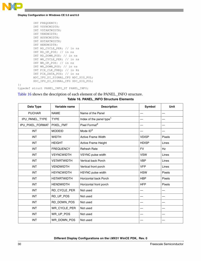
4.2.6.1 PANEL_INFO
PANEL_INFO is the main structure for LCD timing and features. It also contains two structures related to the signals polarity. One of them is not used because it is used for asynchronous displays. SDC_IPU_DI_SIGNAL_CFG on the other hand, describes the polarities and characteristics of the RGB interface, while using a synchronous display panel.
struct PANEL_INFO_ST {PUCHAR NAME;IPU_PANEL_TYPE TYPE;IPU_PIXEL_FORMAT PIXEL_FMT;INT MODEID;INT WIDTH;INT HEIGHT;
Different Display Configurations on the i.MX31 WinCE PDK, Rev. 0
30 Freescale Semiconductor
Display Configuration in Windows CE 5.0 and 6.0
INT FREQUENCY;INT VSYNCWIDTH;INT VSTARTWIDTH;INT VENDWIDTH;INT HSYNCWIDTH;INT HSTARTWIDTH;INT HENDWIDTH;INT RD_CYCLE_PER; // in nsINT RD_UP_POS; // in nsINT RD_DOWN_POS; // in nsINT WR_CYCLE_PER; // in nsINT WR_UP_POS; // in nsINT WR_DOWN_POS; // in nsINT PIX_CLK_FREQ; // in HzINT PIX_DATA_POS; // in nsADC_IPU_DI_SIGNAL_CFG ADC_SIG_POL;SDC_IPU_DI_SIGNAL_CFG SDC_SIG_POL;
};typedef struct PANEL_INFO_ST PANEL_INFO;
Table 16 shows the description of each element of the PANEL_INFO structure.Table 16. PANEL_INFO Structure Elements
Data Type Variable name Description Symbol Unit
PUCHAR NAME Name of the Panel — —
IPU_PANEL_TYPE TYPE Index of the panel type1 — —
IPU_PIXEL_FORMAT PIXEL_FMT Pixel Format2 — —
INT MODEID Mode ID3 — —
INT WIDTH Active Frame Width VDISP Pixels
INT HEIGHT Active Frame Height HDISP Lines
INT FREQUENCY Refresh Rate FV Hz
INT VSYNCWIDTH VSYNC pulse width VSW Lines
INT VSTARTWIDTH Vertical back Porch VBP Lines
INT VENDWIDTH Vertical front porch VFP Lines
INT HSYNCWIDTH HSYNC pulse width HSW Pixels
INT HSTARTWIDTH Horizontal back Porch HBP Pixels
INT HENDWIDTH Horizontal front porch HFP Pixels
INT RD_CYCLE_PER Not used — —
INT RD_UP_POS Not used — —
INT RD_DOWN_POS Not used — —
INT WR_CYCLE_PER Not used — —
INT WR_UP_POS Not used — —
INT WR_DOWN_POS Not used — —
Different Display Configurations on the i.MX31 WinCE PDK, Rev. 0
Freescale Semiconductor 31
Display Configuration in Windows CE 5.0 and 6.0
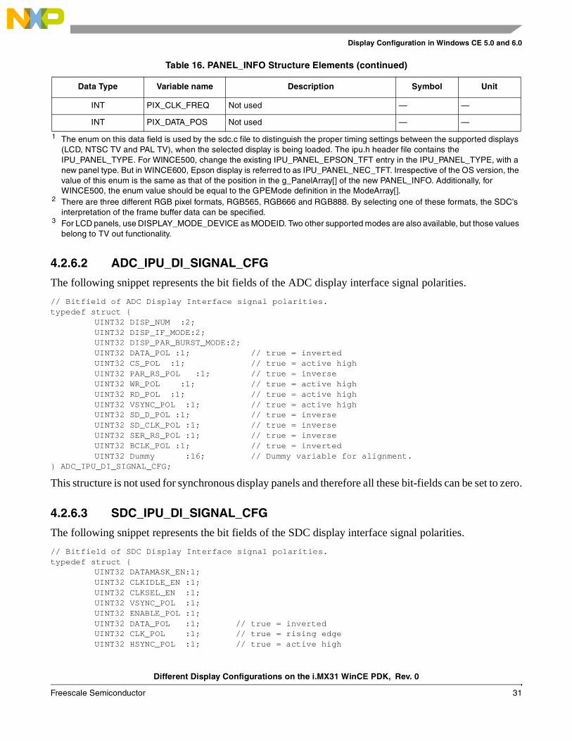
4.2.6.2 ADC_IPU_DI_SIGNAL_CFG
The following snippet represents the bit fields of the ADC display interface signal polarities.
// Bitfield of ADC Display Interface signal polarities.typedef struct {
UINT32 DISP_NUM :2;UINT32 DISP_IF_MODE:2;UINT32 DISP_PAR_BURST_MODE:2;UINT32 DATA_POL :1; // true = invertedUINT32 CS_POL :1; // true = active highUINT32 PAR_RS_POL :1; // true = inverseUINT32 WR_POL :1; // true = active highUINT32 RD_POL :1; // true = active highUINT32 VSYNC_POL :1; // true = active highUINT32 SD_D_POL :1; // true = inverseUINT32 SD_CLK_POL :1; // true = inverseUINT32 SER_RS_POL :1; // true = inverseUINT32 BCLK_POL :1; // true = invertedUINT32 Dummy :16; // Dummy variable for alignment.
} ADC_IPU_DI_SIGNAL_CFG;
This structure is not used for synchronous display panels and therefore all these bit-fields can be set to zero.
4.2.6.3 SDC_IPU_DI_SIGNAL_CFG
The following snippet represents the bit fields of the SDC display interface signal polarities.
// Bitfield of SDC Display Interface signal polarities.typedef struct {
UINT32 DATAMASK_EN:1;UINT32 CLKIDLE_EN :1;UINT32 CLKSEL_EN :1;UINT32 VSYNC_POL :1;UINT32 ENABLE_POL :1;UINT32 DATA_POL :1; // true = invertedUINT32 CLK_POL :1; // true = rising edgeUINT32 HSYNC_POL :1; // true = active high
INT PIX_CLK_FREQ Not used — —
INT PIX_DATA_POS Not used — —
1 The enum on this data field is used by the sdc.c file to distinguish the proper timing settings between the supported displays (LCD, NTSC TV and PAL TV), when the selected display is being loaded. The ipu.h header file contains the IPU_PANEL_TYPE. For WINCE500, change the existing IPU_PANEL_EPSON_TFT entry in the IPU_PANEL_TYPE, with a new panel type. But in WINCE600, Epson display is referred to as IPU_PANEL_NEC_TFT. Irrespective of the OS version, the value of this enum is the same as that of the position in the g_PanelArray[] of the new PANEL_INFO. Additionally, for WINCE500, the enum value should be equal to the GPEMode definition in the ModeArray[].
2 There are three different RGB pixel formats, RGB565, RGB666 and RGB888. By selecting one of these formats, the SDC’s interpretation of the frame buffer data can be specified.
3 For LCD panels, use DISPLAY_MODE_DEVICE as MODEID. Two other supported modes are also available, but those values belong to TV out functionality.
Table 16. PANEL_INFO Structure Elements (continued)
Data Type Variable name Description Symbol Unit

Different Display Configurations on the i.MX31 WinCE PDK, Rev. 0
32 Freescale Semiconductor
Display Configuration in Windows CE 5.0 and 6.0
UINT32 Dummy :24; // Dummy variable for alignment.} SDC_IPU_DI_SIGNAL_CFG;
Table 17 shows the description of each element of the SDC display interface.
4.2.6.4 GPEMode
The following snippet represents the bit fields of the GPEMode interface signal polarities.
// STRUCT GPEMode//// This structure describes a display mode.struct GPEMode{
int modeId;int width;int height;int Bpp;
Table 17. SDC Display Interface Structure Elements
Offset Bit-field Name Description Symbol Polarity
0 DATAMASK_EN Data mask for the display 3 (not used)1
1 Data mask is used to mask the data output to zero, for the sharp TFT power-off sequence. Since this is not a SHARP display this bit-field is not relevant, because of that it should be set to zero (DATAMASK_EN = FALSE).
— —
1 CLKIDLE_EN Display 3 interface clock idle enable2
2 Setting CLKIDLE_EN to FALSE enables the pixel clock when VSYNC is active; using 1 disables the pixel clock during this time. Most of the LCD panels show that pixel clock signal should be present while VSYNC is active (CLKIDLE_EN = FALSE).
— —
2 CLKSEL_EN Select Display 3 interface clock3
3 Selects whether to enable or disable display clock when there is no data output. Set CLKSEL_EN to zero when you always want to enable pixel clock even if there is no data output (Data Enable active). Setting CLKSEL_EN to 1 disables pixel clock when there is no data output. Most of the LCD panels show that pixel clock signal should be present always is active (CLKSEL_EN = FALSE).
— —
3 VSYNC_POL VSYNC signal polarity4
4 Setting VSYNC_POL to FALSE when VSYNC signal is active low. And TRUE when this signal is active in high. See section 2.4.2.1 Vertical timing for details.
VSP —
4 ENABLE_POL Data Enable Polarity5
5 Setting ENABLE_POL to FALSE when DRDY signal is active low. And TRUE when this signal is active in high. See section 2.4.2.2 Horizontal timing to review the details.
DEP —
5 DATA_POL Data Polarity6
6 Setting DATA_POL to FALSE when using straight RGB Data Polarity. And TRUE when data polarity is inverted. See section 2.4.2.2 Horizontal timing.
DP —
6 CLK_POL Clock Polarity7
7 For straight clock polarity set CLK_POL bit-field as FALSE in. For inverse clock polarity set CLK_POL as TRUE. For details please refer to section 2.4.2.3 Pixel Clock timing.
CLKPOL —
7 HSYNC_POL HSYNC signal polarity8
8 Setting HSYNC_POL to FALSE when VSYNC signal is active low. And TRUE when HSYNC when this signal is active in high. Review section 2.4.2.4 Data Polarity.
HSP —
8 Dummy Not used — —

Different Display Configurations on the i.MX31 WinCE PDK, Rev. 0
Freescale Semiconductor 33
Display Configuration in Windows CE 5.0 and 6.0
int frequency;EGPEFormat format;
};
The GPEMode structure specifies the size and format of the screen to the WinCE graphics engine. Using this information, the OS creates frames with the proper size as required by the i.MX31 processor, which is to be processed and sent to the panel using the display interface.
Table 18 shows GPEMode structure members.I
It is important to mention that the i.MX31 supports only 18-bits maximum, as the display interface width. If more than 18-bits are used as BPP, then the less significant bits are discarded, while they are being sent to the LCD. Due to this reason, the recommended values for this field are gpe16Bpp or gpe24Bpp.
enum EGPEFormat{
gpe1Bpp,gpe2Bpp,gpe4Bpp,gpe8Bpp,gpe16Bpp,gpe24Bpp,gpe32Bpp,gpe16YCrCb,gpeDeviceCompatible,gpeUndefined
};
4.2.7 BSP InitializationAfter sdc.c file is properly modified by modifying the g_PanelArray with the new PANEL_INFO structure, it is also necessary to implement the specific LCD panel initialization sequence. Things such as reset, signal enabling and SPI initialization must also be added during the LCD driver load process.
Table 18. GPEMode Structure Members
Data type Variable name Description Symbol Unit
int modeId Display, or TV modes1
1 Display mode can be either DISPLAY_MODE_DEVICE or DISPLAY_MODE_NTSC.
— —
int width Active Frame Width VDISP Pixels
int height Active Frame Height HDISP Lines
int Bpp Bits per pixel2
2 This value should be set to DISP_BPP which value is 16.
— —
int frequency Screen Refresh Rate FV Hz
int Format EGPEFormat enum3
3 This field represents the bits per pixel of the GPE frames and it could be any of the following values.
— —

Different Display Configurations on the i.MX31 WinCE PDK, Rev. 0
34 Freescale Semiconductor
Display Configuration in Windows CE 5.0 and 6.0
4.2.7.1 WINCE500 BSP Initialization
EnableSDC() function configures the LCD interface, but extra pins and interfaces related with the panel are configured in BSPInitializeLCD() function. The original BSP includes the code for the configuration of the CSPI module because the Epson LCD screen needs the serial commands during the initialization. It also configures LCS1 as RESET signal. This code would act as a reference for the new LCD sequence. In case, SPI is not needed the CSPI configuration should be removed. The same situation could happen with the reset signal. It is strongly recommended to add extra hardware to control the Panel ignition using an i.MX31 pin, if the LCD panel does not provide a power off signal or sequence.
After all pins and interfaces are configured BSPEnableLCD() calls DisplayOn() function where LCD power enable, Reset, and SPI commands occur. Fortunately, the code included for the Epson LCD driver acts as a base for the development because reset and SPI commands are implemented for this panel.
4.2.7.2 WINCE600 BSP Initialization
The DDIPU::InitHardware function calls the DDKClockSetpointRequest function to configure the IPU based clock (HSP_CLK) to 132 MHz. Then, the BSPInitializeLCD function is called. This function configures the CSPI interface pins, reset pin, and the LCD data enable pin. After this, the InitializeSDC function is executed and the SDC and DI are configured. Also, the IDMA controller is configured and enabled for the synchronous display controller channel. Then, BSPEnableLCD(eIPU_SDC)function is called with the purpose of configuring the PMIC voltages, the CSPI interface for LCD serial initialization commands, resetting the module and sending the serial commands to the LCD. Finally the EnableSDC function is executed to configure the RGB interface pins (LD0-LD17, VSYNC, HSYNC, DRDY, CONTRAST, and so on) and also the SDC and DI modules are enabled. After all these initializations are complete, the IPU modules, WinCE frames, and LCD are properly initialized and work together to provide the graphic user interface for the system.
4.2.8 Modifying Windows Register and the Catalog
After the sdc.c, ddipu_sdc.cpp (WINCE500 only), ipu.h, and bspdisplay.cpp files are modified, it is very useful to modify the windows register and the catalog. The idea is to replace the existing EPSON L4F00242T03 entries with the new LCD labels. Otherwise, it is confusing to find out which LCD driver is loaded. Both register and catalog should indicate that a new LCD is being used and the EPSON driver is not included anymore.
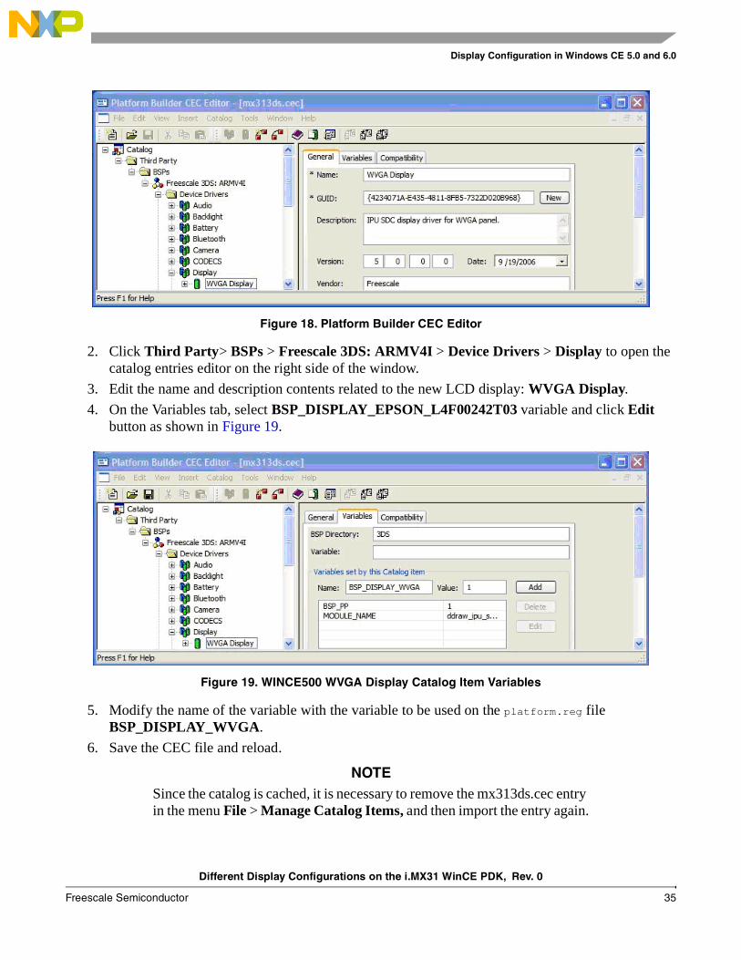
4.2.9 Modifying the WINCE500 CatalogThe epson display driver is found under Third Party > BSPs > Freescale 3DS: ARMV4I > Device Drivers > EPSON L4F00242T03 (VGA). This entry can be changed to avoid any confusion regarding the LCD panel model. Figure 18 shows how WVGA display is used as an example. The procedure to modify WINCE500 catalog is as follows:
1. On platform builder, click the menu Tools > CEC Editor and open 3DS cec file:C:\WINCE500\PUBLIC\COMMON\OAK\CATALOG\CEC\mx313ds.cec
Different Display Configurations on the i.MX31 WinCE PDK, Rev. 0
Freescale Semiconductor 35
Display Configuration in Windows CE 5.0 and 6.0
Figure 18. Platform Builder CEC Editor
2. Click Third Party> BSPs > Freescale 3DS: ARMV4I > Device Drivers > Display to open the catalog entries editor on the right side of the window.
3. Edit the name and description contents related to the new LCD display: WVGA Display.
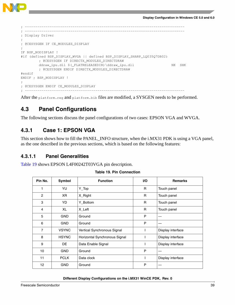
4. On the Variables tab, select BSP_DISPLAY_EPSON_L4F00242T03 variable and click Edit button as shown in Figure 19.
Figure 19. WINCE500 WVGA Display Catalog Item Variables
5. Modify the name of the variable with the variable to be used on the platform.reg file BSP_DISPLAY_WVGA.
6. Save the CEC file and reload.
NOTESince the catalog is cached, it is necessary to remove the mx313ds.cec entry in the menu File > Manage Catalog Items, and then import the entry again.

Different Display Configurations on the i.MX31 WinCE PDK, Rev. 0
36 Freescale Semiconductor
Display Configuration in Windows CE 5.0 and 6.0
4.2.10 Modifying the WINCE600 CatalogThe WINCE600 catalog is changed by using the Microsoft Visual Studio. The procedure to modify WINCE600 catalog using Microsoft Visual Studio is as follows:
1. If the iMX313DS mobility project is open, click File > Close Solution to close the project.
2. Click File > Open > File to open the catalog file under \WINCE600\PLATFORM\iMX313DS\CATALOG folder as shown in Figure 20.
Figure 20. Opening Catalog File
3. Modify the display entry located on Catalog > Third Party > BSP > Freescale i.MX31 3DS: ARMV4I > Device Drivers > Display > EPSON L4F00242T03(VGA).Modify the Title and Description fields, and then click on additional variables collection to modify the BSP_DISPLAY_EPSON_L4F00242T03 using the BSP_DISPLAY_WVGA flag as shown in Figure 21.
Figure 21. WINCE600 WVGA Catalog Item Properties

Different Display Configurations on the i.MX31 WinCE PDK, Rev. 0
Freescale Semiconductor 37
Display Configuration in Windows CE 5.0 and 6.0
4. Click OK on the variables collection message box, save the file and close the file.
5. Open the iMX313DS mobility project and refresh the catalog, by using the button on the top of the catalog items view.
When the iMX313DS mobility project in the visual studio is opened again, it is noticed that the catalog is changed. Now, EPSON Display entry is replaced by the WVGA option. WVGA entry is excluded from the build and this is because you have to modify the platform.bib file. Also, the platform.reg file must be modified.
4.2.11 Platform.regThe following sections describes the WINCE500 platform.reg and WINCE600 platform.reg.
4.2.11.1 WINCE500 Platform.reg
This is the original register entry for the i.MX31 PDK Epson display driver:
IF BSP_DISPLAY_EPSON_L4F00242T03; @XIPREGION IF PACKAGE_OEMDRIVERS[HKEY_LOCAL_MACHINE\Drivers\Display\DDIPU_SDC]
"Bpp"=dword:10 ; 16bpp"PanelType"=dword:1 ; Epson VGA Panel"VideoMemSize"=dword:450000 ; 4.3MB ; To play D1 video
; @XIPREGION ENDIF PACKAGE_OEMDRIVERSENDIF
If the Epson PANEL_INFO in sdc.c is replaced with the new PANEL_INFO structure and if the catalog has been updated already, then the entry looks something similar to this:
IF BSP_DISPLAY_WVGA; @XIPREGION IF PACKAGE_OEMDRIVERS[HKEY_LOCAL_MACHINE\Drivers\Display\DDIPU_SDC]
"Bpp"=dword:10 ; 16bpp"PanelType"=dword:1 ; WVGA Panel"VideoMemSize"=dword:450000 ; 4.3MB ; To play D1 video
; @XIPREGION ENDIF PACKAGE_OEMDRIVERSENDIF
Note that the PanelType index is the same for both LCDs. This is because, both are in the first element of the g_PanelArray[] and one is the replacement of the other.
4.2.11.2 WINCE600 Platform.reg
For adding the support for a new display, open the platform.reg file and replace all BSP_DISPLAY_EPSON_L4F00242T03 entries with the BSP_DISPLAY_WVGA labels. This is the registry entry for the EPSON panel type in WINCE600. Notice that the VideoMemSize variable is not included and this is because the size is extracted from the image_cfg.h file, which was mentioned earlier.
IF BSP_DISPLAY_EPSON_L4F00242T03[HKEY_LOCAL_MACHINE\Drivers\Display\DDIPU]
"Bpp"=dword:10 ; 16bpp"VideoBpp"=dword:10 ; RGB565

Different Display Configurations on the i.MX31 WinCE PDK, Rev. 0
38 Freescale Semiconductor
Display Configuration in Windows CE 5.0 and 6.0
"PanelType"=dword:1 ; Epson VGA dumb PanelENDIF
The new entry looks something similar to this:
IF BSP_DISPLAY_WVGA[HKEY_LOCAL_MACHINE\Drivers\Display\DDIPU]
"Bpp"=dword:10 ; 16bpp"VideoBpp"=dword:10 ; RGB565"PanelType"=dword:1 ; WVGA Panel
ENDIF
4.2.12 Platform.bibThe platform.bib determines the files that are to be included in the image. For display driver, the ddraw_ipu.dll and ipu_base.dll files has to be included. Also, the platform.bib entries must be updated by replacing the two BSP_DISPLAY_EPSON_L4F00242T03 with the BSP_DISPLAY_WVGA.
4.2.12.1 WINCE500 Platform.bib
To accomplish the following data, change the IPU common driver and the display driver entries:
;; display driver;; @CESYSGEN IF CE_MODULES_DISPLAYIF BSP_NODISPLAY !IF BSP_MBX !#if (defined BSP_DISPLAY_NEC_NL6448BC20 || defined BSP_DISPLAY_WVGA); @CESYSGEN IF DIRECTX_MODULES_DIRECTDRAW; @XIPREGION IF PACKAGE_OEMDRIVERS
ddraw_ipu_sdc.dll $(_FLATRELEASEDIR)\ddraw_ipu_sdc.dll NK SH; @XIPREGION ENDIF PACKAGE_OEMDRIVERS; @CESYSGEN ENDIF DIRECTX_MODULES_DIRECTDRAW#endif;; IPU Common driver;; @XIPREGION IF PACKAGE_OEMDRIVERS#if ( defined BSP_CAMERA || defined BSP_PP || defined BSP_DISPLAY_NEC_NL6448BC20 || definedBSP_DISPLAY_WVGA || defined BSP_MBX || defined BSP_ULDR )
ipu_base.dll $(_FLATRELEASEDIR)\ipu_base.dll NK SH#endif; @XIPREGION ENDIF PACKAGE_OEMDRIVERS
4.2.12.2 WINCE600 Platform.bib
To accomplish the following data, change the IPU common driver and the display driver entries:
; -----------------------------------------------------------------------------; IPU Common Driver;#if ( defined BSP_CAMERA || defined BSP_PP || defined BSP_DISPLAY_WVGA || defined BSP_DISPLAY_SHARP_LQ035Q7DB02 || defined BSP_MBX )
ipu_base.dll $(_FLATRELEASEDIR)\ipu_base.dll NK SHK#endif
Different Display Configurations on the i.MX31 WinCE PDK, Rev. 0
Freescale Semiconductor 39
Display Configuration in Windows CE 5.0 and 6.0
; -----------------------------------------------------------------------------; -----------------------------------------------------------------------------; Display Driver;; @CESYSGEN IF CE_MODULES_DISPLAY;IF BSP_NODISPLAY !#if (defined BSP_DISPLAY_WVGA || defined BSP_DISPLAY_SHARP_LQ035Q7DB02)
; @CESYSGEN IF DIRECTX_MODULES_DIRECTDRAWddraw_ipu.dll $(_FLATRELEASEDIR)\ddraw_ipu.dll NK SHK; @CESYSGEN ENDIF DIRECTX_MODULES_DIRECTDRAW
#endifENDIF ; BSP_NODISPLAY !;; @CESYSGEN ENDIF CE_MODULES_DISPLAY; -----------------------------------------------------------------------------
After the platform.reg and platform.bib files are modified, a SYSGEN needs to be performed.
4.3 Panel ConfigurationsThe following sections discuss the panel configurations of two cases: EPSON VGA and WVGA.
4.3.1 Case 1: EPSON VGAThis section shows how to fill the PANEL_INFO structure, when the i.MX31 PDK is using a VGA panel, as the one described in the previous sections, which is based on the following features:
4.3.1.1 Panel Generalities
Table 19 shows EPSON L4F00242T03VGA pin description.
Table 19. Pin Connection
Pin No. Symbol Function I/O Remarks
1 YU Y_Top R Touch panel
2 XR X_Right R Touch panel
3 YD Y_Bottom R Touch panel
4 XL X_Left R Touch panel
5 GND Ground P —
6 GND Ground P —
7 VSYNC Vertical Synchronous Signal I Display interface
8 HSYNC Horizontal Synchronous Signal I Display interface
9 DE Data Enable Signal I Display interface
10 GND Ground P —
11 PCLK Data clock I Display interface
12 GND Ground P —

Different Display Configurations on the i.MX31 WinCE PDK, Rev. 0
40 Freescale Semiconductor
Display Configuration in Windows CE 5.0 and 6.0
13 B0 Display Data I Blue Data LSB
14 B1 Display Data I Blue Data
15 B2 Display Data I Blue Data
16 B3 Display Data I Blue Data
17 B4 Display Data I Blue Data
18 B5 Display Data I Blue Data LSB
19 GND Ground P —
20 G0 Display Data I Green Data LSB
21 G1 Display Data I Green Data
22 G2 Display Data I Green Data
23 G3 Display Data I Green Data
24 G4 Display Data I Green Data
25 G5 Display Data I Green Data LSB
26 GND Ground P —
27 R0 Display Data I Red Data LSB
28 R1 Display Data I Red Data
29 R2 Display Data I Red Data
30 R3 Display Data I Red Data
31 R4 Display Data I Red Data
32 R5 Display Data I Red Data LSB
33 GND Ground P —
34 XRESET Reset I L: reset active
35 XCS Chip select I L: Chip Select active
36 SCLK Serial Clock I Command Interface
37 DIN Serial Data I Command Interface
38 NC — N.C. Not connected
39 GND Ground P —
40 VDDI VDDI P 1.8V
41 VDDI VDDI P 1.8V
42 VDD VDD P 2.8V
43 VDD VDD P 2.8V
44 LED_K LED_Cathode P Cathode
45 LED_A LED_Anode P Anode
Table 19. Pin Connection (continued)
Pin No. Symbol Function I/O Remarks

Different Display Configurations on the i.MX31 WinCE PDK, Rev. 0
Freescale Semiconductor 41
Display Configuration in Windows CE 5.0 and 6.0
Also, consider the Figure 4, LCD interface between the i.MX31 and Epson L4F00242T03 VGA Panel. The timing features of this panel and the Display Interface structures are filled using the following values shown in Table 20, Table 21 and Table 22:
4.3.1.2 Panel Configuration
In a very high perspective, the panel timing and characteristics must be set for the new panel, by modifying the PANEL_INFO into the g_PanelArray[] array. Also, ensure that the GPEMode ModeArray[] is properly configured for the VGA resolution.
Table 20. EPSON L4F00242T03VGA Display Timing
Parameter Symbol Min Typ Max Unit
Screen Height or Vertical cycle VP — 665 — Line
Active Frame Height VDISP — 640 — Line
VSYNC pulse width VSW 5 10 15 Line
Vertical back Porch VBP 5 10 15 Line
Vertical front porch VFP 5 5 5 Line
Vertical refresh rate FV — 60 — Hz
Screen Width or Horizontal cycle HP — 601 — PIXCLK
Active Frame Width HDISP — 480 — PIXCLK
HSYNC pulse width HSW 5 20 75 PIXCLK
Horizontal back Porch HBP 5 60 75 PIXCLK
Horizontal front porch HFP 5 41 111 PIXCLK
Pixel Clock Frequency PCLK — 24 — MHz
Table 21. EPSON L4F00242T03VGA Display Waveform Polarities
Parameter Symbol Polarity
HSYNC Polarity HSP Active LOW
VSYNC Polarity VSP Active LOW
DRDY (Data Enable) Polarity
DEP Active High
Pixel Clock Polarity CLKPOL Inverse Polarity
Data Polarity DP Straight Polarity
Table 22. i.MX31 DISP3 Clock Characteristics
Parameter Symbol Enable/Disable
Display 3 clock idle enable[1] CLKIDLE_EN Enable
Select Display 3 interface clock[2] CLKSEL_EN Enable

Different Display Configurations on the i.MX31 WinCE PDK, Rev. 0
42 Freescale Semiconductor
Display Configuration in Windows CE 5.0 and 6.0
ipu.h (WINCE500)
typedef enum {#ifdef MGN_TFT /*for MX31 build*/
IPU_PANEL_NEW_TFT, // Registry value is 0#else
IPU_PANEL_SHARP_TFT, // Registry value is 0#endif
IPU_PANEL_NEC_TFT, // Registry value is 1IPU_TV_NTSC, // Registry value is 2IPU_TV_PAL, // Registry value is 3ADCPanelOffset,IPU_PANEL_TOSHIBA, // Registry value is 5IPU_PANEL_EPSON, // Registry value is 6// New panel goes here , // Registry value is 4// New panel goes here , // Registry value is 5numPanel,
} IPU_PANEL_TYPE;
In WINCE500, first change to BSP that needs to be performed which is related with the new IPU_PANEL_TYPE. Replace the existing IPU_PANEL_EPSON_TFT by using a panel type name (IPU_PANEL_NEW_TFT) enumeration. This helps to differentiate the panels from other panel types, during initialization.
ipu.h (WINCE600)
// Enumeration of Synchronous (Memory-less) panel types// add name of a new panel in the following format// IPU_PANEL_<Name>_TFT
typedef enum {IPU_PANEL_SHARP_TFT, // Registry value is 0IPU_PANEL_NEW_TFT, // Registry value is 1IPU_TV_NTSC, // Registry value is 2IPU_TV_PAL, // Registry value is 3ADCPanelOffset,IPU_PANEL_TOSHIBA, // Registry value is 5IPU_PANEL_EPSON, // Registry value is 6// New panel goes here , // Registry value is 4// New panel goes here , // Registry value is 5numPanel,
} IPU_PANEL_TYPE;
In WINCE600, replace the existing IPU_PANEL_NEC_TFT (used for Epson panel type) by using a panel type name (IPU_PANEL_NEW_TFT) enumeration. This helps to differentiate the panels from other panel types, during initialization.
sdc.c
PANEL_INFO for the VGA panel timing has to be something similar to this. In WINCE500, this structure must be placed in the first element of the g_PanelArray[], replacing the original EPSON VGA Panel PANEL_INFO. Likewise for WINCE600, the new PANEL_INFO replaces the second element of the EPSON VGA Panel array.
PANEL_INFO g_PanelArray[numPanel] ={

Different Display Configurations on the i.MX31 WinCE PDK, Rev. 0
Freescale Semiconductor 43
Display Configuration in Windows CE 5.0 and 6.0
{"NEW VGA Panel", // NameIPU_PANEL_NEW_TFT, // typeIPU_PIX_FMT_RGB565, // Pixel FormatDISPLAY_MODE_DEVICE, // Mode ID480, // width640, // height60, // frequency10, // Vertical Sync width10, // Vertical Start Width (Back Porch)5, // Vertical End Width (Front Porch)20, // Horizontal Sync Width20, // Horizontal Start Width (Back Porch)111, // Horizontal End Width (Front Porch)0, // Write Cycle Period0, // Write Up Position0, // Write Down Position0, // Read Cycle Period0, // Read Up Position0, // Read Down Position0, // Pixel Clock Cycle Frequency0, // Pixel Data Offset Position{ // ADC Display Interface signal polarities
0,0,0,0,0,0,0,0,0,0,0,0,0,
},{ // Display Interface signal polarities
FALSE, // Data is not masked to zeroFALSE, // PIXCLK present when VSYNC activeFALSE, // PIXCLK present when DE inactive FALSE, // VSYNC is active LOWTRUE, // Data enable is active HIGHFALSE, // Straight Data PolarityTRUE, // Inverse Clock PolarityFALSE, // HSYNC is active LOW
}},
Modify the InitializeSDC function to configure the i.MX31 registers, with the proper values for the interface with the new LCD panel. In WINCE500, the process is to search all IPU_PANEL_EPSON_TFT instances in the sdc.c file. Three occurrences are found and each of these are included as part of a switch sentence. Also, replace all IPU_PANEL_EPSON_TFT enumerations with the new IPU_PANEL_NEW_TFT. For WINCE600, replace IPU_PANEL_NEC_TFT with IPU_PANEL_NEW_TFT entries.

Different Display Configurations on the i.MX31 WinCE PDK, Rev. 0
44 Freescale Semiconductor
Display Configuration in Windows CE 5.0 and 6.0
UINT32 InitializeSDC(PANEL_INFO *currentPanel, int bpp){. . . .case IPU_PANEL_NEW_TFT:. . . .break;
. . . .case IPU_PANEL_NEW_TFT:. . . .break;
. . . .case IPU_PANEL_NEW_TFT:. . . .
break;. . . .}
The only consideration that must be looked upon is the calculation of the pixel clock divider. This divider is automatically calculated by the driver using the timing settings for the display. However, in some cases based on the timing characteristics, the i.MX31 does not provide the frequency that was requested for that specific frame rate. If the frame rate requested is too high, the pixel clock is forced to run at the maximum speed of 33.25 MHz (HSP_CLK/4 = 133MHz/4). With this change, the pixel clock frequency runs at lower frequency than specified. Many LCD’s are able to work even when this pixel clock frequency is lower than the minimum value, specified on the datasheet.
NOTEContact the LCD panel vendor to verify this fact.
The consequences of this adjustment has an impact on the frame rate and it is lower than the number that is set on the PANEL_INFO structure.
sdc.h
The below mentioned #define statements are required only for WINCE500 BSP.
#define SCREEN_PIX_WIDTH 480#define SCREEN_PIX_HEIGHT 640
ddipu_sdc.cpp
The ModeArray is used only in WINCE500. For WINCE600, GPEMode is automatically set by the driver using the width and height described in the PANEL_INFO.
static GPEMode ModeArray[numPanels] ={
// VGA panel{DISPLAY_MODE_DEVICE,SCREEN_PIX_WIDTH,SCREEN_PIX_HEIGHT,DISP_BPP,60, gpe16Bpp},// NEW VGA panel{DISPLAY_MODE_DEVICE,SCREEN_PIX_WIDTH_VGA,SCREEN_PIX_HEIGHT_VGA,DISP_BPP,60,
gpe16Bpp}// Put other panel info here in future expansion// ... ...
};
The GPEMode array for the portrait VGA panels is similar to the code shown above.

Different Display Configurations on the i.MX31 WinCE PDK, Rev. 0
Freescale Semiconductor 45
Display Configuration in Windows CE 5.0 and 6.0
4.3.1.3 Driver Development Process
In WINCE500, the LCD interface is configured in the EnableSDC function. For WINCE600, the pin configuration is set in another file (bspdisplay.cpp). Additionally, this LCD needs the BSP to configure the CSPI interface and reset pin.
sdc.c (WINCE500)
void EnableSDC(void){
UINT32 iOldVal, iNewVal, iMask, iBitval;DWORD dwBytesTransferred;// Configure IOMUX to request IPU SDC pinsDDKIomuxSetPinMux(DDK_IOMUX_PIN_LD0, DDK_IOMUX_OUT_FUNC, DDK_IOMUX_IN_FUNC);DDKIomuxSetPinMux(DDK_IOMUX_PIN_LD1, DDK_IOMUX_OUT_FUNC, DDK_IOMUX_IN_FUNC);DDKIomuxSetPinMux(DDK_IOMUX_PIN_LD2, DDK_IOMUX_OUT_FUNC, DDK_IOMUX_IN_FUNC);DDKIomuxSetPinMux(DDK_IOMUX_PIN_LD3, DDK_IOMUX_OUT_FUNC, DDK_IOMUX_IN_FUNC);DDKIomuxSetPinMux(DDK_IOMUX_PIN_LD4, DDK_IOMUX_OUT_FUNC, DDK_IOMUX_IN_FUNC);DDKIomuxSetPinMux(DDK_IOMUX_PIN_LD5, DDK_IOMUX_OUT_FUNC, DDK_IOMUX_IN_FUNC);DDKIomuxSetPinMux(DDK_IOMUX_PIN_LD6, DDK_IOMUX_OUT_FUNC, DDK_IOMUX_IN_FUNC);DDKIomuxSetPinMux(DDK_IOMUX_PIN_LD7, DDK_IOMUX_OUT_FUNC, DDK_IOMUX_IN_FUNC);DDKIomuxSetPinMux(DDK_IOMUX_PIN_LD8, DDK_IOMUX_OUT_FUNC, DDK_IOMUX_IN_FUNC);DDKIomuxSetPinMux(DDK_IOMUX_PIN_LD9, DDK_IOMUX_OUT_FUNC, DDK_IOMUX_IN_FUNC);DDKIomuxSetPinMux(DDK_IOMUX_PIN_LD10, DDK_IOMUX_OUT_FUNC, DDK_IOMUX_IN_FUNC);DDKIomuxSetPinMux(DDK_IOMUX_PIN_LD11, DDK_IOMUX_OUT_FUNC, DDK_IOMUX_IN_FUNC);DDKIomuxSetPinMux(DDK_IOMUX_PIN_LD12, DDK_IOMUX_OUT_FUNC, DDK_IOMUX_IN_FUNC);DDKIomuxSetPinMux(DDK_IOMUX_PIN_LD13, DDK_IOMUX_OUT_FUNC, DDK_IOMUX_IN_FUNC);DDKIomuxSetPinMux(DDK_IOMUX_PIN_LD14, DDK_IOMUX_OUT_FUNC, DDK_IOMUX_IN_FUNC);DDKIomuxSetPinMux(DDK_IOMUX_PIN_LD15, DDK_IOMUX_OUT_FUNC, DDK_IOMUX_IN_FUNC);DDKIomuxSetPinMux(DDK_IOMUX_PIN_LD16, DDK_IOMUX_OUT_FUNC, DDK_IOMUX_IN_FUNC);DDKIomuxSetPinMux(DDK_IOMUX_PIN_LD17, DDK_IOMUX_OUT_FUNC, DDK_IOMUX_IN_FUNC);DDKIomuxSetPinMux(DDK_IOMUX_PIN_VSYNC3, DDK_IOMUX_OUT_FUNC, DDK_IOMUX_IN_FUNC);DDKIomuxSetPinMux(DDK_IOMUX_PIN_HSYNC, DDK_IOMUX_OUT_FUNC, DDK_IOMUX_IN_FUNC);DDKIomuxSetPinMux(DDK_IOMUX_PIN_FPSHIFT,DDK_IOMUX_OUT_FUNC, DDK_IOMUX_IN_FUNC);DDKIomuxSetPinMux(DDK_IOMUX_PIN_DRDY0, DDK_IOMUX_OUT_FUNC, DDK_IOMUX_IN_FUNC);DDKIomuxSetPinMux(DDK_IOMUX_PIN_D3_REV, DDK_IOMUX_OUT_FUNC, DDK_IOMUX_IN_FUNC);DDKIomuxSetPinMux(DDK_IOMUX_PIN_CONTRAST,DDK_IOMUX_OUT_FUNC,DDK_IOMUX_IN_FUNC);DDKIomuxSetPinMux(DDK_IOMUX_PIN_D3_SPL, DDK_IOMUX_OUT_FUNC, DDK_IOMUX_IN_FUNC);DDKIomuxSetPinMux(DDK_IOMUX_PIN_D3_CLS, DDK_IOMUX_OUT_FUNC, DDK_IOMUX_IN_FUNC);. . . .
}
bspdisplay.cpp (WINCE600)
In WINCE600, BSPDisplayIOMUXEnable function is called by the EnableSDC function. For WINCE500, this function was not included and due to this, pin configuration was performed on sdc.c file.
void BSPDisplayIOMUXEnable(IPU_DRIVE_TYPE dispType){switch (dispType){case eIPU_ADC:. . . . break;case eIPU_SDC:
// Configure IOMUX to request IPU SDC pins

Different Display Configurations on the i.MX31 WinCE PDK, Rev. 0
46 Freescale Semiconductor
Display Configuration in Windows CE 5.0 and 6.0
DDKIomuxSetPinMux(DDK_IOMUX_PIN_LD0, DDK_IOMUX_OUT_FUNC, DDK_IOMUX_IN_FUNC);DDKIomuxSetPinMux(DDK_IOMUX_PIN_LD1, DDK_IOMUX_OUT_FUNC, DDK_IOMUX_IN_FUNC);DDKIomuxSetPinMux(DDK_IOMUX_PIN_LD2, DDK_IOMUX_OUT_FUNC, DDK_IOMUX_IN_FUNC);DDKIomuxSetPinMux(DDK_IOMUX_PIN_LD3, DDK_IOMUX_OUT_FUNC, DDK_IOMUX_IN_FUNC);DDKIomuxSetPinMux(DDK_IOMUX_PIN_LD4, DDK_IOMUX_OUT_FUNC, DDK_IOMUX_IN_FUNC);DDKIomuxSetPinMux(DDK_IOMUX_PIN_LD5, DDK_IOMUX_OUT_FUNC, DDK_IOMUX_IN_FUNC);DDKIomuxSetPinMux(DDK_IOMUX_PIN_LD6, DDK_IOMUX_OUT_FUNC, DDK_IOMUX_IN_FUNC);DDKIomuxSetPinMux(DDK_IOMUX_PIN_LD7, DDK_IOMUX_OUT_FUNC, DDK_IOMUX_IN_FUNC);DDKIomuxSetPinMux(DDK_IOMUX_PIN_LD8, DDK_IOMUX_OUT_FUNC, DDK_IOMUX_IN_FUNC);DDKIomuxSetPinMux(DDK_IOMUX_PIN_LD9, DDK_IOMUX_OUT_FUNC, DDK_IOMUX_IN_FUNC);DDKIomuxSetPinMux(DDK_IOMUX_PIN_LD10, DDK_IOMUX_OUT_FUNC, DDK_IOMUX_IN_FUNC);DDKIomuxSetPinMux(DDK_IOMUX_PIN_LD11, DDK_IOMUX_OUT_FUNC, DDK_IOMUX_IN_FUNC);DDKIomuxSetPinMux(DDK_IOMUX_PIN_LD12, DDK_IOMUX_OUT_FUNC, DDK_IOMUX_IN_FUNC);DDKIomuxSetPinMux(DDK_IOMUX_PIN_LD13, DDK_IOMUX_OUT_FUNC, DDK_IOMUX_IN_FUNC);DDKIomuxSetPinMux(DDK_IOMUX_PIN_LD14, DDK_IOMUX_OUT_FUNC, DDK_IOMUX_IN_FUNC);DDKIomuxSetPinMux(DDK_IOMUX_PIN_LD15, DDK_IOMUX_OUT_FUNC, DDK_IOMUX_IN_FUNC);DDKIomuxSetPinMux(DDK_IOMUX_PIN_LD16, DDK_IOMUX_OUT_FUNC, DDK_IOMUX_IN_FUNC);DDKIomuxSetPinMux(DDK_IOMUX_PIN_LD17, DDK_IOMUX_OUT_FUNC, DDK_IOMUX_IN_FUNC);DDKIomuxSetPinMux(DDK_IOMUX_PIN_VSYNC3, DDK_IOMUX_OUT_FUNC, DDK_IOMUX_IN_FUNC);DDKIomuxSetPinMux(DDK_IOMUX_PIN_HSYNC, DDK_IOMUX_OUT_FUNC, DDK_IOMUX_IN_FUNC);DDKIomuxSetPinMux(DDK_IOMUX_PIN_FPSHIFT, DDK_IOMUX_OUT_FUNC, DDK_IOMUX_IN_FUNC);DDKIomuxSetPinMux(DDK_IOMUX_PIN_DRDY0, DDK_IOMUX_OUT_FUNC, DDK_IOMUX_IN_FUNC);DDKIomuxSetPinMux(DDK_IOMUX_PIN_D3_REV, DDK_IOMUX_OUT_FUNC, DDK_IOMUX_IN_FUNC);DDKIomuxSetPinMux(DDK_IOMUX_PIN_CONTRAST,DDK_IOMUX_OUT_FUNC, DDK_IOMUX_IN_FUNC);DDKIomuxSetPinMux(DDK_IOMUX_PIN_D3_SPL, DDK_IOMUX_OUT_FUNC, DDK_IOMUX_IN_FUNC);DDKIomuxSetPinMux(DDK_IOMUX_PIN_D3_CLS, DDK_IOMUX_OUT_FUNC, DDK_IOMUX_IN_FUNC);g_bSDCEnabled = TRUE;break;
}}
bspdisplay.cpp (WINCE500)
The BSPInitializeLCD function configures the CSPI interface, enable signal and reset pin.
BOOL BSPInitializeLCD(){
PHYSICAL_ADDRESS phyAddr;. . . . // CSPI pins
// CSPI clock pin: DSR_DCE1DDKIomuxSetPinMux(DDK_IOMUX_PIN_DSR_DCE1, DDK_IOMUX_OUT_ALT1, DDK_IOMUX_IN_ALT1);// CSPI data pin: DTR_DTE1// CSPI chip select pin: DTR_DCE2// These 2 pins are controlled through GPR reg bits!// Enable CSPI1 signals on ¡°Full UART¡± pads on HW1 modeDDKIomuxSetGprBit(DDK_IOMUX_GPR_CSPI_BB, 1);
// Reset pin:LCS1, MCU3_24DDKIomuxSetPinMux(DDK_IOMUX_PIN_LCS1, DDK_IOMUX_OUT_GPIO, DDK_IOMUX_IN_GPIO);DDKIomuxSetPadConfig(DDK_IOMUX_PAD_LCS1,DDK_IOMUX_PAD_SLEW_SLOW, DDK_IOMUX_PAD_DRIVE_NORMAL,DDK_IOMUX_PAD_MODE_CMOS,DDK_IOMUX_PAD_TRIG_SCHMITT, DDK_IOMUX_PAD_PULL_UP_100K);DDKGpioSetConfig(DDK_GPIO_PORT3,LCD_RESET_GPIO_PIN,DDK_GPIO_DIR_OUT, DDK_GPIO_INTR_NONE);DDKGpioWriteDataPin(DDK_GPIO_PORT3, LCD_RESET_GPIO_PIN, 1);//in-active// Data Enable Pin:SER_RS, MCU3_25DDKIomuxSetPinMux(DDK_IOMUX_PIN_SER_RS, DDK_IOMUX_OUT_GPIO, DDK_IOMUX_IN_GPIO);DDKIomuxSetPadConfig(DDK_IOMUX_PAD_SER_RS,DDK_IOMUX_PAD_SLEW_SLOW, DDK_IOMUX_PAD_DRIVE_NORMAL,DDK_IOMUX_PAD_MODE_CMOS,DDK_IOMUX_PAD_TRIG_SCHMITT,
Different Display Configurations on the i.MX31 WinCE PDK, Rev. 0
Freescale Semiconductor 47
Display Configuration in Windows CE 5.0 and 6.0
DDK_IOMUX_PAD_PULL_UP_100K);DDKGpioSetConfig(DDK_GPIO_PORT3,LCD_DE_GPIO_PIN,DDK_GPIO_DIR_OUT, DDK_GPIO_INTR_NONE);DDKGpioWriteDataPin(DDK_GPIO_PORT3, LCD_DE_GPIO_PIN, 0); //in-active
bspdisplay.cpp (WINCE600)
For WINCE600, BSPInitializeLCD (IPU_DRIVE_TYPE dispType) function has been modified to initialize the SDC and ADC (Asynchronous Display Controller) interfaces. Due to this, it looks different since it receives a variable which indicates which interface should be configured. For SDC CSPI interface, enable signal and reset pin are configured.
BOOL BSPInitializeLCD(IPU_DRIVE_TYPE dispType){
PHYSICAL_ADDRESS phyAddr;. . . .switch (dispType){
case eIPU_ADC:break;
case eIPU_SDC:if (g_pCSPI == NULL){
//Init CSPI-related pins// CSPI clock pin: DSR_DCE1DDKIomuxSetPinMux(DDK_IOMUX_PIN_DSR_DCE1, DDK_IOMUX_OUT_ALT1, DDK_IOMUX_IN_ALT1);// CSPI data pin: DTR_DTE1// CSPI chip select pin: DTR_DCE2// These 2 pins are controlled through GPR reg bits!// Enable CSPI1 signals on ¡°Full UART¡± pads on HW1 modeDDKIomuxSetGprBit(DDK_IOMUX_GPR_CSPI_BB, 1);
// Reset pin:LCS1, MCU3_24DDKIomuxSetPinMux(DDK_IOMUX_PIN_LCS1, DDK_IOMUX_OUT_GPIO, DDK_IOMUX_IN_GPIO);DDKIomuxSetPadConfig(DDK_IOMUX_PAD_LCS1,DDK_IOMUX_PAD_SLEW_SLOW, DDK_IOMUX_PAD_DRIVE_NORMAL, DDK_IOMUX_PAD_MODE_CMOS, DDK_IOMUX_PAD_TRIG_SCHMITT, DDK_IOMUX_PAD_PULL_UP_100K);DDKGpioSetConfig(DDK_GPIO_PORT3, LCD_RESET_GPIO_PIN, DDK_GPIO_DIR_OUT, DDK_GPIO_INTR_NONE);DDKGpioWriteDataPin(DDK_GPIO_PORT3, LCD_RESET_GPIO_PIN, 1);//in-active// Data Enable Pin:SER_RS, MCU3_25DDKIomuxSetPinMux(DDK_IOMUX_PIN_SER_RS, DDK_IOMUX_OUT_GPIO, DDK_IOMUX_IN_GPIO);DDKIomuxSetPadConfig(DDK_IOMUX_PAD_SER_RS, DDK_IOMUX_PAD_SLEW_SLOW, DDK_IOMUX_PAD_DRIVE_NORMAL, DDK_IOMUX_PAD_MODE_CMOS, DDK_IOMUX_PAD_TRIG_SCHMITT, DDK_IOMUX_PAD_PULL_UP_100K);DDKGpioSetConfig(DDK_GPIO_PORT3,LCD_DE_GPIO_PIN,DDK_GPIO_DIR_OUT, DDK_GPIO_INTR_NONE);DDKGpioWriteDataPin(DDK_GPIO_PORT3, LCD_DE_GPIO_PIN, 0); //in-active. . . .}
Finally, in WINCE500, DisplayOn function generates the reset signal and the SPI commands are sent to the LCD.
bspdisplay.cpp
static void DisplayOn(void){. . . .
// Reset LCD module, MCU3_24, LOW activeDDKGpioWriteDataPin(DDK_GPIO_PORT3, LCD_RESET_GPIO_PIN, 0);

Different Display Configurations on the i.MX31 WinCE PDK, Rev. 0
48 Freescale Semiconductor
Display Configuration in Windows CE 5.0 and 6.0
Sleep(100);DDKGpioWriteDataPin(DDK_GPIO_PORT3, LCD_RESET_GPIO_PIN, 1);Sleep(100);//Data Enable signal is set to always HIGH active, MCU3_25DDKGpioWriteDataPin(DDK_GPIO_PORT3, LCD_DE_GPIO_PIN, 1);
. . . .// Config CSPI registers OUTREG32(&g_pCSPI->CONREG, LCD_CSPI_CONFIG);OUTREG32(&g_pCSPI->DMAREG, LCD_CSPI_FUNCTION_OFF);OUTREG32(&g_pCSPI->INTREG, LCD_CSPI_FUNCTION_OFF);OUTREG32(&g_pCSPI->TESTREG, LCD_CSPI_FUNCTION_OFF);//Enable CSPIINSREG32BF(&g_pCSPI->CONREG, CSPI_CONREG_EN, CSPI_CONREG_EN_ENABLE);
. . . .// MADCTLLCD_CSPI_Write(0x00000036);LCD_CSPI_Write(madCtrl);// GAMSET: 0x1LCD_CSPI_Write(0x00000026);LCD_CSPI_Write(0x00000100);// COLMOD: 0x50 - RGB565LCD_CSPI_Write(0x0000003A);LCD_CSPI_Write(0x00000150);// PASETLCD_CSPI_Write(0x0000002B);LCD_CSPI_Write(0x00000100);LCD_CSPI_Write(0x00000100);LCD_CSPI_Write(paMax_Hi);LCD_CSPI_Write(paMax_Low);// CASETLCD_CSPI_Write(0x0000002A);LCD_CSPI_Write(0x00000100);LCD_CSPI_Write(0x00000100);LCD_CSPI_Write(caMax_Hi);LCD_CSPI_Write(caMax_Low);// SLPOUTLCD_CSPI_Write(0x00000011);Sleep(100);// DISONLCD_CSPI_Write(0x00000029);Sleep(100);// Disable CSPIINSREG32BF(&g_pCSPI->CONREG, CSPI_CONREG_EN, CSPI_CONREG_EN_DISABLE);// Disable CSPI's clock
DDKClockSetGatingMode(DDK_CLOCK_GATE_INDEX_CSPI1, DDK_CLOCK_GATE_MODE_DISABLED);. . . .}
In WINCE600, DisplayOn function does not exist. The PMIC settings, Reset signal, Enable signal and SPI commands are performed by the BSPEnableLCD (IPU_DRIVE_TYPE dispType) function. This function has also changed from the WINCE500 version. As a result, a display type is received as a parameter to indicate which LCD panel should be initialized, which LCD controls the SDC or which LCD is driven by the ADC.
BOOL BSPEnableLCD(IPU_DRIVE_TYPE dispType){
if (g_pPBC == NULL)

Different Display Configurations on the i.MX31 WinCE PDK, Rev. 0
Freescale Semiconductor 49
Display Configuration in Windows CE 5.0 and 6.0
{return FALSE;
}switch (dispType){
case eIPU_SDC:// Turn on LCD via PBC//OUTREG16(&g_pPBC->BCTRL1_SET, CSP_BITFMASK(PBC_BCTRL1_SET_LCDON));{
PMIC_REGULATOR_VREG_VOLTAGE voltage;UINT32 paMax_Hi, paMax_Low, caMax_Hi, caMax_Low, madCtrl;// Configure PMIC to turn on LCD's power supply// VGEN: 1.8 V// VMMC1: 2.8VPmicVoltageRegulatorOn(VMMC1);PmicVoltageRegulatorOn(VGEN);voltage.vmmc = VMMC_6;//2.8VPmicVoltageRegulatorSetVoltageLevel(VMMC1, voltage);voltage.vgen = VGEN_1_80V;PmicVoltageRegulatorSetVoltageLevel(VGEN, voltage);Sleep(100);
//Reset LCD module, MCU3_24, LOW activeDDKGpioWriteDataPin(DDK_GPIO_PORT3, LCD_RESET_GPIO_PIN, 0);Sleep(100);DDKGpioWriteDataPin(DDK_GPIO_PORT3, LCD_RESET_GPIO_PIN, 1);Sleep(100);//Data Enable signal is set to always HIGH active, MCU3_25DDKGpioWriteDataPin(DDK_GPIO_PORT3, LCD_DE_GPIO_PIN, 1);
WaitForSingleObject(g_hCspiMutex, INFINITE);//Enable CSPI's clockDDKClockSetGatingMode(DDK_CLOCK_GATE_INDEX_CSPI1,
DDK_CLOCK_GATE_MODE_ENABLED_ALL);//Config CSPI registers OUTREG32(&g_pCSPI->CONREG, LCD_CSPI_CONFIG);OUTREG32(&g_pCSPI->DMAREG, LCD_CSPI_FUNCTION_OFF);OUTREG32(&g_pCSPI->INTREG, LCD_CSPI_FUNCTION_OFF);OUTREG32(&g_pCSPI->TESTREG, LCD_CSPI_FUNCTION_OFF);//Enable CSPIINSREG32BF(&g_pCSPI->CONREG, CSPI_CONREG_EN, CSPI_CONREG_EN_ENABLE);//LCD Power ON sequence//// bit[8] indicates if it's command or parameter, | 0x100
#if 1// 0/180 degree, portraitmadCtrl = 0x00000100; //0x000001D0paMax_Hi = 0x00000100;paMax_Low = 0x0000019F;caMax_Hi = 0x00000101;caMax_Low = 0x000001DF;
#else// 90/270 degree, landscapemadCtrl = 0x000001B0;// 0x000000160paMax_Hi = 0x00000101;

Different Display Configurations on the i.MX31 WinCE PDK, Rev. 0
50 Freescale Semiconductor
Display Configuration in Windows CE 5.0 and 6.0
paMax_Low = 0x000001DF ;caMax_Hi = 0x00000100;caMax_Low = 0x0000019F;
#endif// MADCTLLCD_CSPI_Write(0x00000036);LCD_CSPI_Write(madCtrl);// GAMSET: 0x1LCD_CSPI_Write(0x00000026);LCD_CSPI_Write(0x00000100);// COLMOD: 0x50 - RGB565LCD_CSPI_Write(0x0000003A);LCD_CSPI_Write(0x00000150);// PASETLCD_CSPI_Write(0x0000002B);LCD_CSPI_Write(0x00000100);LCD_CSPI_Write(0x00000100);LCD_CSPI_Write(paMax_Hi);LCD_CSPI_Write(paMax_Low);// CASETLCD_CSPI_Write(0x0000002A);LCD_CSPI_Write(0x00000100);LCD_CSPI_Write(0x00000100);LCD_CSPI_Write(caMax_Hi);LCD_CSPI_Write(caMax_Low);// SLPOUTLCD_CSPI_Write(0x00000011);Sleep(100);// DISONLCD_CSPI_Write(0x00000029);Sleep(100);// Disable CSPIINSREG32BF(&g_pCSPI->CONREG, CSPI_CONREG_EN, CSPI_CONREG_EN_DISABLE);// Disable CSPI's clockDDKClockSetGatingMode(DDK_CLOCK_GATE_INDEX_CSPI1,
DDK_CLOCK_GATE_MODE_DISABLED);ReleaseMutex(g_hCspiMutex);//setting SW1 work on PWM mode(High power)//PmicSwitchModeRegulatorSetMode(SW1A, LOW, SW_MODE_PWM);
}. . . .
platform.reg (WINCE500)
If the display catalog entry is already replaced with the new panel variable, then the platform.reg file should also be modified to indicate that a new panel is being loaded in the platform.
IF BSP_DISPLAY_NEW_VGA; @XIPREGION IF PACKAGE_OEMDRIVERS[HKEY_LOCAL_MACHINE\Drivers\Display\DDIPU_SDC]
"Bpp"=dword:10 ; 16bpp"PanelType"=dword:1 ; New VGA Panel "VideoMemSize"=dword:450000 ; 4.3MB ; To play D1 video
; @XIPREGION ENDIF PACKAGE_OEMDRIVERSENDIF

Different Display Configurations on the i.MX31 WinCE PDK, Rev. 0
Freescale Semiconductor 51
Display Configuration in Windows CE 5.0 and 6.0
platform.reg (WINCE600)
IF BSP_DISPLAY_NEW_VGA[HKEY_LOCAL_MACHINE\Drivers\Display\DDIPU]
"Bpp"=dword:10 ; 16bpp"VideoBpp"=dword:10 ; RGB565"PanelType"=dword:1 ; New VGA Panel
ENDIF
platform.bib (WINCE500)
Platform image builder file should be updated for including the display driver when the new WVGA catalog item is selected.
;; display driver;; @CESYSGEN IF CE_MODULES_DISPLAYIF BSP_NODISPLAY !IF BSP_MBX !#if (defined BSP_DISPLAY_NEC_NL6448BC20 || defined BSP_DISPLAY_NEW_VGA); @CESYSGEN IF DIRECTX_MODULES_DIRECTDRAW; @XIPREGION IF PACKAGE_OEMDRIVERSddraw_ipu_sdc.dll $(_FLATRELEASEDIR)\ddraw_ipu_sdc.dll NK SH; @XIPREGION ENDIF PACKAGE_OEMDRIVERS; @CESYSGEN ENDIF DIRECTX_MODULES_DIRECTDRAW#endif
;; IPU Common driver;; @XIPREGION IF PACKAGE_OEMDRIVERS#if ( defined BSP_CAMERA || defined BSP_PP || defined BSP_DISPLAY_NEC_NL6448BC20 || defined BSP_DISPLAY_NEW_VGA || defined BSP_MBX || defined BSP_ULDR )ipu_base.dll $(_FLATRELEASEDIR)\ipu_base.dll NK SH #endif; @XIPREGION ENDIF PACKAGE_OEMDRIVERS
platform.bib (WINCE600)
To accomplish the following data, change the IPU common driver and the display driver entries:
; -----------------------------------------------------------------------------; IPU Common Driver;#if ( defined BSP_CAMERA || defined BSP_PP || defined BSP_DISPLAY_NEW_VGA || defined BSP_DISPLAY_SHARP_LQ035Q7DB02 || defined BSP_MBX )ipu_base.dll $(_FLATRELEASEDIR)\ipu_base.dll NK SHK#endif; -----------------------------------------------------------------------------; -----------------------------------------------------------------------------; Display Driver;; @CESYSGEN IF CE_MODULES_DISPLAY;IF BSP_NODISPLAY !#if (defined BSP_DISPLAY_NEW_VGA || defined BSP_DISPLAY_SHARP_LQ035Q7DB02); @CESYSGEN IF DIRECTX_MODULES_DIRECTDRAW

Different Display Configurations on the i.MX31 WinCE PDK, Rev. 0
52 Freescale Semiconductor
Display Configuration in Windows CE 5.0 and 6.0
ddraw_ipu.dll $(_FLATRELEASEDIR)\ddraw_ipu.dll NK SHK; @CESYSGEN ENDIF DIRECTX_MODULES_DIRECTDRAW#endifENDIF ; BSP_NODISPLAY !;; @CESYSGEN ENDIF CE_MODULES_DISPLAY; -----------------------------------------------------------------------------
4.3.2 Case 2: WVGAThis section shows how to fill the PANEL_INFO structure, when the i.MX31 PDK is using a WVGA panel based on the following features.
4.3.2.1 Panel Generalities
CLAA070VC01 is 7 inch color Thin Film Transistor Liquid Crystal Display (TFT-LCD) module composed of the LCD panel, driver ICs, control circuit, and LED backlight. The 7 inch screen produces a high resolution image composed of 800×480 pixel elements in a stripe arrangement and a display of 262K colors by 6-bit RG.B signal input.
Table 23 shows the CLAA070VC01 pin connection layout.
Table 23. Pin Connection
PIN No. Symbol Description I/O
1 Vss Power Ground P
2 Vss Power Ground P
3 ADJ Brightness control for LED B/L P
4 VDD Power Supply for LED Driver Circuit P
5 VDD Power Supply for LED Driver Circuit P
6 VDD Power Supply for LED Driver Circuit P
7 Vcc Power Supply for digital Circuit P
8 Vcc Power Supply for digital Circuit P
9 DE Data Enable I
10 Vss Power Ground P
11 Vss Power Ground P
12 Vss Power Ground P
13 B5 Blue Data 5 (MSB) I
14 B4 Blue Data 4 I
15 B3 Blue Data 3 I
16 Vss Power Ground P
17 B2 Blue Data 2 I
18 B1 Blue Data 1 I

Different Display Configurations on the i.MX31 WinCE PDK, Rev. 0
Freescale Semiconductor 53
Display Configuration in Windows CE 5.0 and 6.0
Table 24 shows the WVGA CLAA070VC01 display timing.
19 B0 Blue Data 0 (LSB) I
20 Vss Power Ground P
21 G5 Green Data 5 (MSB) I
22 G4 Green Data 4 I
23 G3 Green Data 3 I
24 Vss Power Ground P
25 G2 Green Data 2 I
26 G1 Green Data 1 I
27 G0 Green Data 0 (LSB) I
28 Vss Power Ground P
29 R5 Red Data 5 (MSB) I
30 R4 Red Data 4 I
31 R3 Red Data 3 I
32 Vss Power Ground P
33 R2 Red Data 2 I
34 R1 Red Data 1 I
35 R0 Red Data 0 (LSB) I
36 Vss Power Ground P
37 Vss Power Ground P
38 DCLK Clock Signals: Latch Data at Falling Edge I
39 Vss Power Ground P
40 Vss Power Ground P
Table 24. WVGA CLAA070VC01 Display Timing
Parameter Symbol Min Typ Max Unit
Screen Height or Vertical cycle VP 490 500 520 Line
Active Frame Height VDISP 480 480 480 Line
VSYNC pulse width VSW 1 1 1 Line
Vertical back Porch VBP 1 10 20 Line
Vertical front porch VFP 0 10 19 Line
Vertical refresh rate FV 55 60 65 Hz
Screen Width or Horizontal cycle HP 850 900 950 PIXCLK
Table 23. Pin Connection (continued)
PIN No. Symbol Description I/O

Different Display Configurations on the i.MX31 WinCE PDK, Rev. 0
54 Freescale Semiconductor
Display Configuration in Windows CE 5.0 and 6.0
Table 25 shows the WVGA CLAA070VC01 display waveform polarities.
Table 26 shows the i.MX31 DISP3 clock characteristics.
4.3.2.2 Panel Configuration
The PANEL_INFO for the WVGA panel is similar to this, and it must be placed in the first element of the g_PanelArray[] replacing the original EPSON VGA Panel PANEL_INFO:
ipu.h (WINCE500)
typedef enum {#ifdef MGN_TFT /*for MX31 build*/
IPU_PANEL_WVGA_TFT, // Registry value is 0 #else
IPU_PANEL_SHARP_TFT, // Registry value is 0#endif
IPU_PANEL_NEC_TFT, // Registry value is 1IPU_TV_NTSC, // Registry value is 2IPU_TV_PAL, // Registry value is 3ADCPanelOffset,IPU_PANEL_TOSHIBA, // Registry value is 5IPU_PANEL_EPSON, // Registry value is 6
Active Frame Width HDISP 800 800 800 PIXCLK
HSYNC pulse width HSW 1 1 1 PIXCLK
Horizontal back Porch HBP 1 50 150 PIXCLK
Horizontal front porch HFP 0 50 149 PIXCLK
Pixel Clock Frequency PCLK 25 27 32 MHz
Table 25. WVGA CLAA070VC01 display waveform polarities
Parameter Symbol Polarity
HSYNC Polarity HSP Active LOW (Imaginary)
VSYNC Polarity VSP Active LOW (Imaginary)
DRDY (Data Enable) Polarity
DEP Active High
Pixel Clock Polarity CLKPOL Straight Polarity
Data Polarity DP Straight Polarity
Table 26. i.MX31 DISP3 Clock Characteristics.
Parameter Symbol Enable/Disable
Display 3 clock idle enable[1] CLKIDLE_EN Enable
Select Display 3 interface clock[2] CLKSEL_EN Enable
Table 24. WVGA CLAA070VC01 Display Timing
Parameter Symbol Min Typ Max Unit

Different Display Configurations on the i.MX31 WinCE PDK, Rev. 0
Freescale Semiconductor 55
Display Configuration in Windows CE 5.0 and 6.0
// New panel goes here , // Registry value is 4// New panel goes here , // Registry value is 5numPanel,
} IPU_PANEL_TYPE;
ipu.h (WINCE600)
// Enumeration of Synchronous (Memory-less) panel types// add name of a new panel in the following format// IPU_PANEL_<Name>_TFTtypedef enum {
IPU_PANEL_SHARP_TFT, // Registry value is 0IPU_PANEL_WVGA_TFT, // Registry value is 1IPU_TV_NTSC, // Registry value is 2IPU_TV_PAL, // Registry value is 3ADCPanelOffset,IPU_PANEL_TOSHIBA, // Registry value is 5IPU_PANEL_EPSON, // Registry value is 6// New panel goes here , // Registry value is 4// New panel goes here , // Registry value is 5numPanel,
} IPU_PANEL_TYPE;
sdc.c
The PANEL_INFO for the WVGA panel timing is similar to this, and it must be placed in the first element of the g_PanelArray[] replacing the original "EPSON VGA Panel" PANEL_INFO. Note that Epson panel is located in the first array position in WINCE500 while it is on second position in WINCE600.
PANEL_INFO g_PanelArray[numPanel] ={
{"NEW WVGA Panel", // NameIPU_PANEL_WVGA_TFT, // typeIPU_PIX_FMT_RGB565, // Pixel FormatDISPLAY_MODE_DEVICE, // Mode ID800, // width480, // height60, // frequency1, // Vertical Sync width10, // Vertical Start Width (Back Porch)10, // Vertical End Width (Front Porch)1, // Horizontal Sync Width50, // Horizontal Start Width (Back Porch)50, // Horizontal End Width (Front Porch)0, // Write Cycle Period0, // Write Up Position0, // Write Down Position0, // Read Cycle Period0, // Read Up Position0, // Read Down Position0, // Pixel Clock Cycle Frequency0, // Pixel Data Offset Position{ // ADC Display Interface signal polarities
0,0,

Different Display Configurations on the i.MX31 WinCE PDK, Rev. 0
56 Freescale Semiconductor
Display Configuration in Windows CE 5.0 and 6.0
0,0,0,0,0,0,0,0,0,0,0,
},{ // Display Interface signal polaritiesFALSE, // Data is not masked to zeroFALSE, // PIXCLK present when VSYNC activeFALSE, // PIXCLK present when DE inactive FALSE, // VSYNC is active LOWTRUE, // Data enable is active HIGHFALSE, // Straight Data PolarityFALSE, // Inverse Clock PolarityFALSE, // HSYNC is active LOW
}},
sdc.h
The below mentioned #define statements are required only for WINCE500 BSP.
#define SCREEN_PIX_WIDTH_WVGA800#define SCREEN_PIX_HEIGHT_WVGA480
ddipu_sdc.cpp
The ModeArray is used only in WINCE500. For WINCE600, GPEMode is automatically set by the driver using the width and height described in the PANEL_INFO.
static GPEMode ModeArray[numPanels] ={
// WVGA panel{DISPLAY_MODE_DEVICE, SCREEN_PIX_WIDTH_WVGA, SCREEN_PIX_HEIGHT_WVGA, DISP_BPP, 60,
gpe16Bpp},// NEW VGA panel{DISPLAY_MODE_DEVICE, SCREEN_PIX_WIDTH_VGA, SCREEN_PIX_HEIGHT_VGA, DISP_BPP, 60,
gpe16Bpp}, //640*480*16bpp// Put other panel info here in future expasion// ... ...
};
4.3.2.3 Driver Development Process
LCD interface is configured on EnableSDC() function in WINCE500. For WINCE600, pin configuration is set in another file (bspdisplay.cpp).

Different Display Configurations on the i.MX31 WinCE PDK, Rev. 0
Freescale Semiconductor 57
Display Configuration in Windows CE 5.0 and 6.0
sdc.c (WINCE500)
void EnableSDC(void){
UINT32 iOldVal, iNewVal, iMask, iBitval;DWORD dwBytesTransferred;// Configure IOMUX to request IPU SDC pinsDDKIomuxSetPinMux(DDK_IOMUX_PIN_LD0, DDK_IOMUX_OUT_FUNC, DDK_IOMUX_IN_FUNC);DDKIomuxSetPinMux(DDK_IOMUX_PIN_LD1, DDK_IOMUX_OUT_FUNC, DDK_IOMUX_IN_FUNC);DDKIomuxSetPinMux(DDK_IOMUX_PIN_LD2, DDK_IOMUX_OUT_FUNC, DDK_IOMUX_IN_FUNC);DDKIomuxSetPinMux(DDK_IOMUX_PIN_LD3, DDK_IOMUX_OUT_FUNC, DDK_IOMUX_IN_FUNC);DDKIomuxSetPinMux(DDK_IOMUX_PIN_LD4, DDK_IOMUX_OUT_FUNC, DDK_IOMUX_IN_FUNC);DDKIomuxSetPinMux(DDK_IOMUX_PIN_LD5, DDK_IOMUX_OUT_FUNC, DDK_IOMUX_IN_FUNC);DDKIomuxSetPinMux(DDK_IOMUX_PIN_LD6, DDK_IOMUX_OUT_FUNC, DDK_IOMUX_IN_FUNC);DDKIomuxSetPinMux(DDK_IOMUX_PIN_LD7, DDK_IOMUX_OUT_FUNC, DDK_IOMUX_IN_FUNC);DDKIomuxSetPinMux(DDK_IOMUX_PIN_LD8, DDK_IOMUX_OUT_FUNC, DDK_IOMUX_IN_FUNC);DDKIomuxSetPinMux(DDK_IOMUX_PIN_LD9, DDK_IOMUX_OUT_FUNC, DDK_IOMUX_IN_FUNC);DDKIomuxSetPinMux(DDK_IOMUX_PIN_LD10, DDK_IOMUX_OUT_FUNC, DDK_IOMUX_IN_FUNC);DDKIomuxSetPinMux(DDK_IOMUX_PIN_LD11, DDK_IOMUX_OUT_FUNC, DDK_IOMUX_IN_FUNC);DDKIomuxSetPinMux(DDK_IOMUX_PIN_LD12, DDK_IOMUX_OUT_FUNC, DDK_IOMUX_IN_FUNC);DDKIomuxSetPinMux(DDK_IOMUX_PIN_LD13, DDK_IOMUX_OUT_FUNC, DDK_IOMUX_IN_FUNC);DDKIomuxSetPinMux(DDK_IOMUX_PIN_LD14, DDK_IOMUX_OUT_FUNC, DDK_IOMUX_IN_FUNC);DDKIomuxSetPinMux(DDK_IOMUX_PIN_LD15, DDK_IOMUX_OUT_FUNC, DDK_IOMUX_IN_FUNC);DDKIomuxSetPinMux(DDK_IOMUX_PIN_LD16, DDK_IOMUX_OUT_FUNC, DDK_IOMUX_IN_FUNC);DDKIomuxSetPinMux(DDK_IOMUX_PIN_LD17, DDK_IOMUX_OUT_FUNC, DDK_IOMUX_IN_FUNC);DDKIomuxSetPinMux(DDK_IOMUX_PIN_FPSHIFT, DDK_IOMUX_OUT_FUNC, DDK_IOMUX_IN_FUNC);DDKIomuxSetPinMux(DDK_IOMUX_PIN_DRDY0, DDK_IOMUX_OUT_FUNC, DDK_IOMUX_IN_FUNC);DDKIomuxSetPinMux(DDK_IOMUX_PIN_D3_REV, DDK_IOMUX_OUT_FUNC, DDK_IOMUX_IN_FUNC);DDKIomuxSetPinMux(DDK_IOMUX_PIN_CONTRAST, DDK_IOMUX_OUT_FUNC, DDK_IOMUX_IN_FUNC);DDKIomuxSetPinMux(DDK_IOMUX_PIN_D3_SPL, DDK_IOMUX_OUT_FUNC, DDK_IOMUX_IN_FUNC);DDKIomuxSetPinMux(DDK_IOMUX_PIN_D3_CLS, DDK_IOMUX_OUT_FUNC, DDK_IOMUX_IN_FUNC);
bspdisplay.cpp (WINCE600)
In WINCE600, BSPDisplayIOMUXEnable function is called by EnableSDC function. For WINCE500, pin configuration is performed on sdc.c because this function is not included.
void BSPDisplayIOMUXEnable(IPU_DRIVE_TYPE dispType){switch (dispType){case eIPU_ADC:. . . .break;case eIPU_SDC:
// Configure IOMUX to request IPU SDC pinsDDKIomuxSetPinMux(DDK_IOMUX_PIN_LD0, DDK_IOMUX_OUT_FUNC, DDK_IOMUX_IN_FUNC);DDKIomuxSetPinMux(DDK_IOMUX_PIN_LD1, DDK_IOMUX_OUT_FUNC, DDK_IOMUX_IN_FUNC);DDKIomuxSetPinMux(DDK_IOMUX_PIN_LD2, DDK_IOMUX_OUT_FUNC, DDK_IOMUX_IN_FUNC);DDKIomuxSetPinMux(DDK_IOMUX_PIN_LD3, DDK_IOMUX_OUT_FUNC, DDK_IOMUX_IN_FUNC);DDKIomuxSetPinMux(DDK_IOMUX_PIN_LD4, DDK_IOMUX_OUT_FUNC, DDK_IOMUX_IN_FUNC);DDKIomuxSetPinMux(DDK_IOMUX_PIN_LD5, DDK_IOMUX_OUT_FUNC, DDK_IOMUX_IN_FUNC);DDKIomuxSetPinMux(DDK_IOMUX_PIN_LD6, DDK_IOMUX_OUT_FUNC, DDK_IOMUX_IN_FUNC);DDKIomuxSetPinMux(DDK_IOMUX_PIN_LD7, DDK_IOMUX_OUT_FUNC, DDK_IOMUX_IN_FUNC);DDKIomuxSetPinMux(DDK_IOMUX_PIN_LD8, DDK_IOMUX_OUT_FUNC, DDK_IOMUX_IN_FUNC);DDKIomuxSetPinMux(DDK_IOMUX_PIN_LD9, DDK_IOMUX_OUT_FUNC, DDK_IOMUX_IN_FUNC);DDKIomuxSetPinMux(DDK_IOMUX_PIN_LD10, DDK_IOMUX_OUT_FUNC, DDK_IOMUX_IN_FUNC);
Different Display Configurations on the i.MX31 WinCE PDK, Rev. 0
58 Freescale Semiconductor
Display Configuration in Windows CE 5.0 and 6.0
DDKIomuxSetPinMux(DDK_IOMUX_PIN_LD11, DDK_IOMUX_OUT_FUNC, DDK_IOMUX_IN_FUNC);DDKIomuxSetPinMux(DDK_IOMUX_PIN_LD12, DDK_IOMUX_OUT_FUNC, DDK_IOMUX_IN_FUNC);DDKIomuxSetPinMux(DDK_IOMUX_PIN_LD13, DDK_IOMUX_OUT_FUNC, DDK_IOMUX_IN_FUNC);DDKIomuxSetPinMux(DDK_IOMUX_PIN_LD14, DDK_IOMUX_OUT_FUNC, DDK_IOMUX_IN_FUNC);DDKIomuxSetPinMux(DDK_IOMUX_PIN_LD15, DDK_IOMUX_OUT_FUNC, DDK_IOMUX_IN_FUNC);DDKIomuxSetPinMux(DDK_IOMUX_PIN_LD16, DDK_IOMUX_OUT_FUNC, DDK_IOMUX_IN_FUNC);DDKIomuxSetPinMux(DDK_IOMUX_PIN_LD17, DDK_IOMUX_OUT_FUNC, DDK_IOMUX_IN_FUNC);DDKIomuxSetPinMux(DDK_IOMUX_PIN_FPSHIFT, DDK_IOMUX_OUT_FUNC, DDK_IOMUX_IN_FUNC);DDKIomuxSetPinMux(DDK_IOMUX_PIN_DRDY0, DDK_IOMUX_OUT_FUNC, DDK_IOMUX_IN_FUNC);DDKIomuxSetPinMux(DDK_IOMUX_PIN_D3_REV, DDK_IOMUX_OUT_FUNC, DDK_IOMUX_IN_FUNC);DDKIomuxSetPinMux(DDK_IOMUX_PIN_CONTRAST,DDK_IOMUX_OUT_FUNC, DDK_IOMUX_IN_FUNC);DDKIomuxSetPinMux(DDK_IOMUX_PIN_D3_SPL, DDK_IOMUX_OUT_FUNC, DDK_IOMUX_IN_FUNC);DDKIomuxSetPinMux(DDK_IOMUX_PIN_D3_CLS, DDK_IOMUX_OUT_FUNC, DDK_IOMUX_IN_FUNC);g_bSDCEnabled = TRUE;
break;}}
Note that either for WINCE500 and WINCE600 VSYNC and HSYNC, pins were not configured because WVGA’s panel interface does not need these signals.
Because this panel does not need a reset signal and SPI initialization, but a power on/off signal was added to the board in order to control the power consumption of this panel (WVGA_PWR_ENABLE_GPIO_PIN).
bspdisplay.cpp (WINCE500)
BOOL BSPInitializeLCD(){
PHYSICAL_ADDRESS phyAddr;if (g_pPBC == NULL){
phyAddr.QuadPart = BSP_BASE_REG_PA_PBC_BASE;// Map PBC registers to virtual address spaceg_pPBC = (PCSP_PBC_REGS) MmMapIoSpace(phyAddr, sizeof(CSP_PBC_REGS), FALSE);
if (g_pPBC == NULL){
DEBUGMSG(GPE_ZONE_ERROR, (TEXT("%s(): MmMapIoSpace failed!\r\n"), __WFUNCTION__));
return FALSE;}
}// WVGA LCD Power EnableDDKIomuxSetPinMux(DDK_IOMUX_PIN_LCS1, DDK_IOMUX_OUT_GPIO, DDK_IOMUX_IN_GPIO);DDKIomuxSetPadConfig(DDK_IOMUX_PAD_LCS1, DDK_IOMUX_PAD_SLEW_SLOW, DDK_IOMUX_PAD_DRIVE_NORMAL, DDK_IOMUX_PAD_MODE_CMOS, DDK_IOMUX_PAD_TRIG_SCHMITT, DDK_IOMUX_PAD_PULL_UP_100K);DDKGpioSetConfig(DDK_GPIO_PORT3, WVGA_PWR_ENABLE_GPIO_PIN, DDK_GPIO_DIR_OUT,DDK_GPIO_INTR_NONE);DDKGpioWriteDataPin(DDK_GPIO_PORT3, WVGA_PWR_ENABLE_GPIO_PIN, 1); // Active-Low}
bspdisplay.cpp (WINCE600)
For WINCE600, BSPInitializeLCD (IPU_DRIVE_TYPE dispType) is modified to initialize SDC and ADC (Asynchronous Display Controller) interfaces. It receives a variable which indicates which interface should be configured. Initialization of LCD panel is similar to WINCE500, beside the power enable signal.

Different Display Configurations on the i.MX31 WinCE PDK, Rev. 0
Freescale Semiconductor 59
Display Configuration in Windows CE 5.0 and 6.0
BOOL BSPInitializeLCD(IPU_DRIVE_TYPE dispType){
PHYSICAL_ADDRESS phyAddr;. . . .switch (dispType){
case eIPU_ADC:break;case eIPU_SDC:
// WVGA LCD Power EnableDDKIomuxSetPinMux(DDK_IOMUX_PIN_LCS1, DDK_IOMUX_OUT_GPIO, DDK_IOMUX_IN_GPIO);DDKIomuxSetPadConfig(DDK_IOMUX_PAD_LCS1, DDK_IOMUX_PAD_SLEW_SLOW, DDK_IOMUX_PAD_DRIVE_NORMAL, DDK_IOMUX_PAD_MODE_CMOS, DDK_IOMUX_PAD_TRIG_SCHMITT, DDK_IOMUX_PAD_PULL_UP_100K);DDKGpioSetConfig(DDK_GPIO_PORT3, WVGA_PWR_ENABLE_GPIO_PIN, DDK_GPIO_DIR_OUT, DDK_GPIO_INTR_NONE);DDKGpioWriteDataPin(DDK_GPIO_PORT3, WVGA_PWR_ENABLE_GPIO_PIN, 1); // Active-Low. . . .}
bspdisplay.cpp
static void DisplayOn(void){
PMIC_REGULATOR_VREG_VOLTAGE voltage;//LCD Power Enable signal (Active-low), MCU3_24, LOW activeDDKGpioWriteDataPin(DDK_GPIO_PORT3, WVGA_PWR_ENABLE_GPIO_PIN, 0);Sleep(100);PmicVoltageRegulatorOn(VMMC1);PmicVoltageRegulatorOn(VGEN);voltage.vmmc = VMMC_6;//2.8VPmicVoltageRegulatorSetVoltageLevel(VMMC1, voltage);voltage.vgen = VGEN_1_80V;PmicVoltageRegulatorSetVoltageLevel(VGEN, voltage);Sleep(100);
}
For WINCE500, DisplayOn() function provides LCD power enable signal in which PMIC voltages are also configured.
In WINCE600, DisplayOn function does not exist. The PMIC settings, Reset signal, Enable signal and SPI commands are performed by BSPEnableLCD(IPU_DRIVE_TYPE dispType). This function has also changed from WINCE500 version. As a result, a display type is received as parameter to indicate which LCD panel should be initialized, the LCD controlled the SDC or the LCD driven by the ADC.
BOOL BSPEnableLCD(IPU_DRIVE_TYPE dispType){
if (g_pPBC == NULL){
return FALSE;}switch (dispType){
case eIPU_SDC:// Turn on LCD via PBC//OUTREG16(&g_pPBC->BCTRL1_SET, CSP_BITFMASK(PBC_BCTRL1_SET_LCDON));
{PMIC_REGULATOR_VREG_VOLTAGE voltage;

Different Display Configurations on the i.MX31 WinCE PDK, Rev. 0
60 Freescale Semiconductor
Display Configuration in Windows CE 5.0 and 6.0
UINT32 paMax_Hi, paMax_Low, caMax_Hi, caMax_Low, madCtrl;// Configure PMIC to turn on LCD's power supply// VGEN: 1.8 V// VMMC1: 2.8VPmicVoltageRegulatorOn(VMMC1);PmicVoltageRegulatorOn(VGEN);voltage.vmmc = VMMC_6;//2.8VPmicVoltageRegulatorSetVoltageLevel(VMMC1, voltage);voltage.vgen = VGEN_1_80V;PmicVoltageRegulatorSetVoltageLevel(VGEN, voltage);Sleep(100);//LCD Power Enable signal (Active-low), MCU3_24, LOW activeDDKGpioWriteDataPin(DDK_GPIO_PORT3, WVGA_PWR_ENABLE_GPIO_PIN, 0);Sleep(100);WaitForSingleObject(g_hCspiMutex, INFINITE);ReleaseMutex(g_hCspiMutex);
}. . . .
platform.reg (WINCE500)
If the display catalog entry is replaced with a new panel variable, then the platform.reg should also modified to indicate that a new panel is being load it in the platform.
IF BSP_DISPLAY_WVGA; @XIPREGION IF PACKAGE_OEMDRIVERS[HKEY_LOCAL_MACHINE\Drivers\Display\DDIPU_SDC]
"Bpp"=dword:10 ; 16bpp"PanelType"=dword:1 ; WVGA Panel "VideoMemSize"=dword:450000 ; 4.3MB ; To play D1 video; @XIPREGION ENDIF PACKAGE_OEMDRIVERSENDIF
platform.reg (WINCE600)
IF BSP_DISPLAY_WVGA[HKEY_LOCAL_MACHINE\Drivers\Display\DDIPU]"Bpp"=dword:10 ; 16bpp"VideoBpp"=dword:10 ; RGB565"PanelType"=dword:1 ; WVGA PanelENDIF
platform.bib (WINCE500)
Platform image builder file should be updated for including the display driver when the new WVGA catalog item is selected.
;; display driver;; @CESYSGEN IF CE_MODULES_DISPLAYIF BSP_NODISPLAY !IF BSP_MBX !#if (defined BSP_DISPLAY_NEC_NL6448BC20 || defined BSP_DISPLAY_WVGA); @CESYSGEN IF DIRECTX_MODULES_DIRECTDRAW; @XIPREGION IF PACKAGE_OEMDRIVERS

Different Display Configurations on the i.MX31 WinCE PDK, Rev. 0
Freescale Semiconductor 61
Summary and Tips
ddraw_ipu_sdc.dll $(_FLATRELEASEDIR)\ddraw_ipu_sdc.dll NK SH; @XIPREGION ENDIF PACKAGE_OEMDRIVERS; @CESYSGEN ENDIF DIRECTX_MODULES_DIRECTDRAW#endif;; IPU Common driver;; @XIPREGION IF PACKAGE_OEMDRIVERS#if ( defined BSP_CAMERA || defined BSP_PP || defined BSP_DISPLAY_NEC_NL6448BC20 || defined BSP_DISPLAY_WVGA || defined BSP_MBX || defined BSP_ULDR )ipu_base.dll $(_FLATRELEASEDIR)\ipu_base.dll NK SH#endif; @XIPREGION ENDIF PACKAGE_OEMDRIVERS
platform.bib (WINCE600)
Change IPU Common driver and Display Driver entries to acomplish with the following data:
; -----------------------------------------------------------------------------; IPU Common Driver;#if ( defined BSP_CAMERA || defined BSP_PP || defined BSP_DISPLAY_WVGA || defined BSP_DISPLAY_SHARP_LQ035Q7DB02 || defined BSP_MBX )ipu_base.dll $(_FLATRELEASEDIR)\ipu_base.dll NK SHK#endif; -----------------------------------------------------------------------------; -----------------------------------------------------------------------------; Display Driver;; @CESYSGEN IF CE_MODULES_DISPLAY;IF BSP_NODISPLAY !#if (defined BSP_DISPLAY_WVGA || defined BSP_DISPLAY_SHARP_LQ035Q7DB02); @CESYSGEN IF DIRECTX_MODULES_DIRECTDRAWddraw_ipu.dll $(_FLATRELEASEDIR)\ddraw_ipu.dll NK SHK; @CESYSGEN ENDIF DIRECTX_MODULES_DIRECTDRAW#endifENDIF ; BSP_NODISPLAY !;; @CESYSGEN ENDIF CE_MODULES_DISPLAY; -----------------------------------------------------------------------------
5 Summary and Tips
5.1 Support for VGA and Bigger PanelsThe i.MX31 supports several LCD resolutions ranging from small panels to a maximum display resolution of SVGA (800×600). However, there are few limitations for this resolution. The following sections explain the possible scenarios that occur when using resolutions above VGA in the i.MX31 platforms.

Different Display Configurations on the i.MX31 WinCE PDK, Rev. 0
62 Freescale Semiconductor
Summary and Tips
5.1.1 Frame RateDepending on the pixel clock, back porch, front porch, and memory interface, the frame rate might decrease to less than 60 fps. For instance, while working on WinCE, the microprocessor creates the frames related to the WinCE desktop and places the images on memory. In this case, incoming frames come from the memory display buffer. An 800×600 frame is periodically created after which the Display Interface (DI) sends this information (probably RGB666 or RGB565), to the VGA, WVGA, or SVGA LCD. DI sends the complete buffer in a little more time than HORIZONTAL_RESOLUTION x VERTICAL_RESOLUTION x PIXCLK period. For example, if using a SVGA panel, the time is the result of 800 x 600 x PIXCLK period (usually 30 ns). That means, one frame every 14.43 ms, or 69 frames per second (fps). However, considering the front and back porch for horizontal and vertical adjustment, it is probable that the frame rate decreases to less than 60 fps.
5.1.2 Image Converter Restrictions for WVGA and SVGAThe biggest limitation in the i.MX31 for bigger LCD panels, is the Image Converter (IC) buffer of the IPU. The maximum frame size after downsizing is up to 720×1024 (See the MCIMX31 and MCIMX31L Applications Processors Reference Manual, Table 44.1.2 (IPU Features)). It is more accurate to say that the IC maximum frame size after either downsizing or upsizing is 720×1024. To make the user aware about this, the IC performs color space conversion, combining (alpha blending), downsizing, upsizing, and other operations over image or video frames. IC is also the IPU's entry point for the camera interface.
This means IPU's Image converter output can not be greater than 720. It is easier to handle portrait orientation WVGA (480×800) or SVGA (600×800) because of the 720×1024 restriction. To process WVGA (800×480) or SVGA (800×600) landscape frames or images using the Image Converter, the i.MX31 has the ability to split the frame buffers, process the buffer sections separately, and then combine them again in a single buffer. For example, to process a SVGA image or frame (CSC, resize, alpha blending, and so on), the i.MX31 splits the frame buffer into two 400×600 parts. Then it reads and begin to process the first half of the image. The complement, at the end of Image DMA Controller (IDMAC) sorts both buffers creating an 800×600 SVGA image. Even when this process is done by the hardware, it duplicates the postprocessors stages two times and decreases the image treatment speed at half of the bandwidth. This bandwidth is not the frame rate, but it is extremely important when a camera is attached to the device or a video playback using image converter.

Different Display Configurations on the i.MX31 WinCE PDK, Rev. 0
Freescale Semiconductor 63
Summary and Tips
Figure 22 shows the image converter process flow of WVGA and SVGA.
Figure 22. Image Converter Process Flow for WVGA and SVGA
However, the upcoming i.MX processors have improved on these characteristics. For example, in the i.MX35, the maximal frame size after resizing is 800×1024.
5.1.3 Memory AccessesThe i.MX31 can create WinCE desktop frames. However, this requires a lot of memory transfers. For example, in a normal SVGA application in the i.MX31 MAX PDK, where the memory interface is a DDR running at 133 MHz, the maximum memory bandwidth is 266,000,000×32 bits (266, because DDR latches data on the rising and falling edge). Even when there is plenty of bandwidth, the display interface shares the memory with the processor and all the peripherals included in the i.MX31.
For WinCE desktops you could calculate the average of percentage of memory that display interface uses to maintain the SVGA interface.
Memory Bandwidth = 266,000,000 × 32 bits = 8,512,000,000 bits per second Eqn. 3
SVGA frame write access = 800 × 600 pixels × 16 bits (RGB565) × 60 fps= 460,800,000 Eqn. 4
SVGA frame read access = 800 × 600 pixels × 16 bits (RGB565) × 60 fps= 460,800,000 Eqn. 5
Percentage of memory used by DI = (460,800,000 × 2) / 8,512,000,000 = 10.83 % Eqn. 6

Different Display Configurations on the i.MX31 WinCE PDK, Rev. 0
64 Freescale Semiconductor
Summary and Tips
460,800,000 is multiplied by two because it is needed first to create the frame (write) and after read the contents from the buffer and send them to the display interface.
The number calculated above is only for the display interface. If there is a post-processing stage (CSC, resize, alpha blending, and so on) for the frames, then another read or write related to each frame is performed. As a result, the display uses 21.66% of the memory bandwidth. If background (WinCE desktop) and foreground (Camera for example) planes are used at the same time, the memory usage also increases. The memory usage depends on how many planes are used and how many times these frames are accessed.
5.1.4 FlickeringFlickering issue occurs because the display interface cannot access its buffer on time, and causes an annoying behavior on the screen. Even when there is plenty of bandwidth, the display interface shares the memory with the processor and all other peripherals included in the i.MX31. Therefore, flickering is not caused due to an IPU issue, but it is caused because of the memory architecture. Even when there is enough bandwidth, the USB interface locks the external memory interface (EMI) and does not allow other interfaces to access RAM memory through AHB while it works. This means that if a platform combines large resolution panels (VGA WVGA or SVGA) and the USB interface this problem occurs. For example, while reading a Windows Media Video file from a USB memory stick connected to a hub also having an external USB keyboard and mouse, it is very probable of recreating the flickering issue. But, while reading the video file from a NAND Flash or SD Card the probabilities of experiencing the flickering issue are very less.This problem only occurs when all these interfaces are put to work at the same time. For example, if the video files from the USB stick are copied to the RAM or NAND Flash and then run from a non-USB location, the flickering does not appear.
NOTEThere is a workaround available (BSP_IRAM_PATCH) for USB flickering issue. Since this is a hardware issue, the patch might affect other components such as the USB throughput.
Another issue is that IPU shares its memory data bus with the WEIM (Wireless External Interface Module). For example, the i.MX31 PDK CPLD is accessed through WEIM and through the Ethernet interface. In this case, there is also the possibility to experience the flickering if both WEIM and display interface are constantly working at the same time. For example, if a Windows Media Video file is read from NOR Flash (not shipped in the i.MX31 PDK) or if the Ethernet interface (i.MX31 PDK) is strongly used in a VGA, WVGA, or SVGA platform, the flickering might appear.
So, flickering is more like a combination of two interfaces, and it is recommended when possible, to avoid the working together of the following two combinations:
1. VGA Display (or bigger) + USB (reading or writing)
2. VGA Display (or bigger) + any interface connected to the WEIM, like NOR Flash or Ethernet in the i.MX31 MAX PDK.

Different Display Configurations on the i.MX31 WinCE PDK, Rev. 0
Freescale Semiconductor 65
References
6 ReferencesFor more information on WINCE600 Display Driver Development Concepts refer to the link below:
• http://msdn.microsoft.com/en-us/library/ee485877.aspx
7 Revision History Table 27 provides a revision history for this application note.
Table 27. Document Revision History
Rev.Number
Date Substantive Change(s)
0 02/2010 Initial release.

Different Display Configurations on the i.MX31 WinCE PDK, Rev. 0
66 Freescale Semiconductor
Revision History
THIS PAGE INTENTIONALLY LEFT BLANK

Different Display Configurations on the i.MX31 WinCE PDK, Rev. 0
Freescale Semiconductor 67
Revision History
THIS PAGE INTENTIONALLY LEFT BLANK

Document Number: AN4041Rev. 003/2010
Information in this document is provided solely to enable system and software
implementers to use Freescale Semiconductor products. There are no express or
implied copyright licenses granted hereunder to design or fabricate any integrated
circuits or integrated circuits based on the information in this document.
Freescale Semiconductor reserves the right to make changes without further notice to
any products herein. Freescale Semiconductor makes no warranty, representation or
guarantee regarding the suitability of its products for any particular purpose, nor does
Freescale Semiconductor assume any liability arising out of the application or use of
any product or circuit, and specifically disclaims any and all liability, including without
limitation consequential or incidental damages. “Typical” parameters which may be
provided in Freescale Semiconductor data sheets and/or specifications can and do
vary in different applications and actual performance may vary over time. All operating
parameters, including “Typicals” must be validated for each customer application by
customer’s technical experts. Freescale Semiconductor does not convey any license
under its patent rights nor the rights of others. Freescale Semiconductor products are
not designed, intended, or authorized for use as components in systems intended for
surgical implant into the body, or other applications intended to support or sustain life,
or for any other application in which the failure of the Freescale Semiconductor product
could create a situation where personal injury or death may occur. Should Buyer
purchase or use Freescale Semiconductor products for any such unintended or
unauthorized application, Buyer shall indemnify and hold Freescale Semiconductor
and its officers, employees, subsidiaries, affiliates, and distributors harmless against all
claims, costs, damages, and expenses, and reasonable attorney fees arising out of,
directly or indirectly, any claim of personal injury or death associated with such
unintended or unauthorized use, even if such claim alleges that Freescale
Semiconductor was negligent regarding the design or manufacture of the part.
How to Reach Us:
Home Page: www.freescale.com
Web Support: http://www.freescale.com/support
USA/Europe or Locations Not Listed: Freescale Semiconductor, Inc.Technical Information Center, EL5162100 East Elliot Road Tempe, Arizona 85284 1-800-521-6274 or+1-480-768-2130www.freescale.com/support
Europe, Middle East, and Africa:Freescale Halbleiter Deutschland GmbHTechnical Information CenterSchatzbogen 781829 Muenchen, Germany+44 1296 380 456 (English) +46 8 52200080 (English)+49 89 92103 559 (German)+33 1 69 35 48 48 (French) www.freescale.com/support
Japan: Freescale Semiconductor Japan Ltd. HeadquartersARCO Tower 15F1-8-1, Shimo-Meguro, Meguro-ku Tokyo 153-0064Japan 0120 191014 or+81 3 5437 [email protected]
Asia/Pacific: Freescale Semiconductor China Ltd. Exchange Building 23FNo. 118 Jianguo RoadChaoyang DistrictBeijing 100022China+86 10 5879 [email protected]
For Literature Requests Only:Freescale Semiconductor
Literature Distribution Center 1-800 441-2447 or+1-303-675-2140Fax: +1-303-675-2150LDCForFreescaleSemiconductor
@hibbertgroup.com
Freescale and the Freescale logo are trademarks or registered trademarks of Freescale Semiconductor, Inc. in the U.S. and other countries. All other product or service names are the property of their respective owners. ARM is the registered trademark of ARM Limited. ARMnnn is the trademark of ARM Limited.
© Freescale Semiconductor, Inc., 2010. All rights reserved.