Embed Size (px)
Citation preview
1 IntroductionAudio output has become an important part of manyembedded applications, such as audio players, voice recorders,VoIP telephony, smart appliances, and electronic toys. Thisapplication note describes the basic methods of implementingaudio output. Modern MCUs, such as the Kinetis family,include powerful CPU cores and specialized peripherals thatallow audio reproduction easily, while requiring a minimum ofexternal hardware.
1.1 AbstractAudio records are usually stored either in the MCU'sembedded flash memory, or externally on an SD-card orexternal EEPROM IC. They are stored as raw audio samplesor in any compressed audio format. This application note doesnot describe the decompression of the compressed audiorecords.
The key element of the process is to use a method oftransferring the stream of decompressed audio data to thedesired output while having a minimal CPU load and no signaldropouts or distortion.
Freescale Semiconductor Document Number: AN4369
Application Note Rev. 0, 02/2012
Audio Output Options for KinetisUsing DMA and PWM, DAC, or I2S Audio Bus
by: Michael GaldaFreescaleRožnov CSCCzech Republic
© 2012 Freescale Semiconductor, Inc.
Contents
1 Introduction................................................................1
2 Double-buffering and DMA......................................2
3 Audio output options.................................................4
4 Audio signal preprocessing.......................................5
5 Demo software example..........................................10
6 Audio output hardware considerations. ..................12
7 Conclusion...............................................................15
8 Testing and validation.............................................15
9 References...............................................................15
One of the recommended methods is to use double-buffering and direct memory access (DMA). In this case the audio datacan be read and processed by the CPU while the DMA hardware state machine feeds the audio output with audio samples inthe background.
Examples of application areas:• Answering machines• VoIP telephony• Safety systems• Smart medical appliances• Voice recorders• Intercoms• Walkie-talkies• Electronic toys
2 Double-buffering and DMAThese software and hardware methods are commonly used in applications that require a continuous data flow while using aminimum of CPU cycles.
2.1 Ping-pong buffersAt any one time, one buffer is actively being played (the front buffer), while the second (background) buffer is filled with thenew audio samples. When playing is completed, the roles of the two buffers are switched. This is usually accomplished byswitching the pointers. See Figure 1 and Figure 2 for details.
2.2 Direct memory access (DMA)Direct memory access is ensured by the DMA controller, which is a special MCU peripheral capable of transferring largeblocks of data between memory locations with no CPU assistance needed.
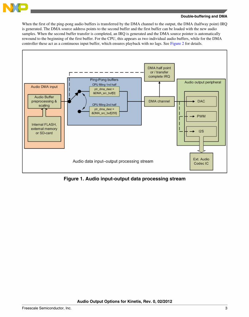
The software initializes a DMA channel with the DMA transfer attributes, the source and destination memory address, thenumber of bytes transferred in the minor loop (single memory access) and the number of minor loops inside the major loop,which defines the total size of the transferred data block. The source/destination address is incremented automatically afterthe completion of every minor loop. When the complete block has been transferred (the major loop done), the IRQ isgenerated by the DMA channel. Two separated or adjacent physical SRAM memory arrays can be used to create two ping-pong buffers.
Some of the DMA peripherals, such as the eDMA module used on Kinetis devices, allow generation of an IRQ on a half-point transfer event. This means that the IRQ will be generated when half of the total transfers have been done (DMA citer =biter/2) and the next IRQ is requested when the major loop is done (after the last transfer).
In our example, we are using a single DMA source buffer, which is split into two parts (the lower half and the upper half).These two subparts are acting as two ping-pong buffers. The source address is set to the beginning of the DMA source audiobuffer. The destination address is the address of the MCU peripheral register responsible for the audio output. In our case itmay be a FlexTimer channel value register (PWM duty register), a DAC output data register, or an I2S transmit data register.The source offset and number of bytes (NBYTES) transferred in a single minor loop is equal to two bytes (16 bits), becausethe source audio samples are 16-bit values.
NOTESome additional audio processing such as oversampling, filtering, output dithering, andsignal value scaling may be required from the CPU.
Double-buffering and DMA
Audio Output Options for Kinetis, Rev. 0, 02/2012
2 Freescale Semiconductor, Inc.
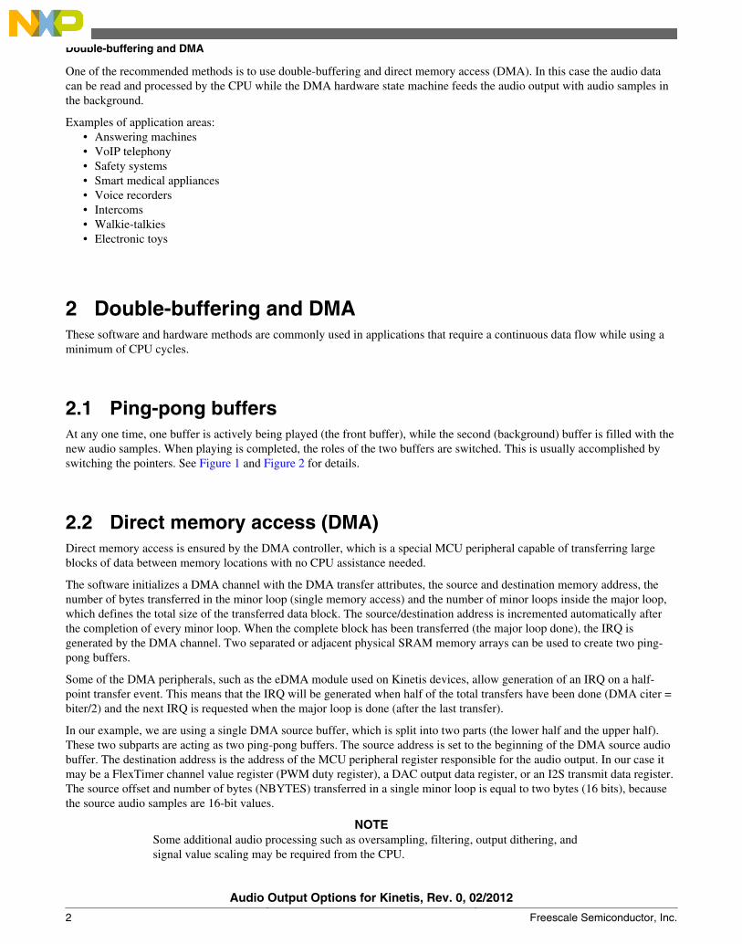
When the first of the ping-pong audio buffers is transferred by the DMA channel to the output, the DMA (halfway point) IRQis generated. The DMA source address points to the second buffer and the first buffer can be loaded with the new audiosamples. When the second buffer transfer is completed, an IRQ is generated and the DMA source pointer is automaticallyrewound to the beginning of the first buffer. For the CPU, this appears as two individual audio buffers, while for the DMAcontroller these act as a continuous input buffer, which ensures playback with no lags. See Figure 2 for details.
Figure 1. Audio input-output data processing stream
Double-buffering and DMA
Audio Output Options for Kinetis, Rev. 0, 02/2012
Freescale Semiconductor, Inc. 3
Figure 2. DMA input buffer in detail
3 Audio output optionsDepending on the required audio output quality, there are several output options possible, such as PWM, DAC, or an externalaudio codec IC through the I2S audio bus. The Kinetis MCU family supports the FlexTimer peripherals, providing severalPWM outputs, 12-bit DAC converters, and a specialized I2S peripheral audio bus interface compatible with an external audiocodec IC.
As mentioned above, the audio output peripheral options for Kinetis devices are:• DAC (12-bit)• PWM (FlexTimer)• I2S (SAI) bus over an external codec IC
3.1 Advantages of the different solutionsPulse width modulation(PWM) output with a simple low-pass filter can be used in a cost-sensitive application. The PWMoutput pins provide enough current to drive the low-impedance speaker directly without an amplifier. Additionally, thecurrent can be boosted by a transistor or op-amp. The key point is to design the output low-pass filter properly considering
Audio output options
Audio Output Options for Kinetis, Rev. 0, 02/2012
4 Freescale Semiconductor, Inc.
the filter cutoff frequency. The main disadvantage to this solution is that the PWM switching frequency should be set higherthan 16 kHz (higher than the audible band). The PWM provides a square signal on the output, which is reconstructed andsmoothed as an acoustic signal after going through the low-pass filter and by the inductance of the speaker coil. The PWMtimer output compare event can trigger the DMA transfer directly.
Digital-to-analog-converter (DAC) output can generate very smooth signals, so it can provide better results than the PWM.The DAC current output capability is very low (maximum 1 mA) , and so it has to be amplified externally. The DAC outputregister has to be periodically reloaded with a new sample by the DMA channel. A single PIT channel or a FlexTimerchannel running in output compare mode, with a period equal to the audio sampling rate, can be used for triggering the DMA.
The Inter-IC Sound (IIS or I2S) bus is a standardized audio data interface commonly used and supported by a number ofexternal audio codec ICs available on the market.
3.2 Output signal resolution versus frequencyPWM output resolution
With the FlexTimer module, we can generate a PWM output signal with a theoretical resolution of up to 16 bits. If the PWMis used for audio output, the PWM reloading frequency (switching frequency) is equal to the audio output sample rate.
Considering the maximum FlexTimer module input frequency (50 MHz on a Kinetis K60 MCU running on a 100 MHzsystem clock), we can generate a 16-bit PWM output with a PWM reload frequency up to 50000000 / 65536 = 763 Hz, whichis of course too low a switching frequency for the audio signal sample rate.
For instance, if we need an output audio sample rate equal to 22 kHz = 22050 Hz, we will get the following equation:50000/22050 = 2268, which is close to ~ 2048 corresponding to 12 bits of PWM resolution.
DAC frequency limits
The Kinetis DAC output resolution is 12-bit only. This means that a 16-bit audio sample value has to be truncated as well.
The DAC setting time is limited. For the Kinetis devices, the data sheet specifies 15–30 µs in hi-speed mode. Practicalmeasurements have confirmed that we can go up to ~50 kHz.
The audio data samples are usually stored in 16-bit signed integer format. For the above-mentioned reasons, the values haveto be scaled (converted to an unsigned integer) and divided to the proper size to be compatible with the PWM or DACoutputs. This is done in the software by adding +32768 and bit-shifting to get the desired output resolution.
Example of output value scaling:
// Convert an audio sample from 16-bit signed to 12-bit unsigned value for PWM or DAC output
*p_audio_dst++ = ((uint16_t)(audsample + 32768))>>4;
I2S data format
I2S data is sent from the MSB to the LSB beginning from the second clock cycle after the word select clock transition. Thetransmitting MSB first allows both the transmitting and receiving devices to not care about the audio precision of the remotedevice. For instance, if the transmitter is sending 32 bits per channel to a device with only 24 or 16 bits of resolution, thereceiving device may simply ignore the extra bits. If the transmitter is sending 16-bit samples per channel to a receivingdevice with 24 bits of precision, the receiver will simply zero-fill the missing bits. Data words are transferred synchronouslyat the frequency equal to the audio sample rate.
4 Audio signal preprocessingDepending on the required input and output audio signal quality, these types of basic signal processing can be done inruntime by the CPU.
• Oversampling
Audio signal preprocessing
Audio Output Options for Kinetis, Rev. 0, 02/2012
Freescale Semiconductor, Inc. 5
• Signal dithering• Digital filtering
4.1 OversamplingOutput oversampling helps avoid aliasing, improves resolution, and reduces noise.
In many applications, a common problem is aliasing. Aliasing causes the presence of higher harmonic components in thesignal spectrum. It can be a bit tricky to create an effective analog filter, given the maximum available bandwidth and sharpcutoff, without exceeding the Nyquist frequency (which is half of the original sampling frequency). By increasing thebandwidth of the sampled signal (increasing the sampling frequency), we can create an anti-aliasing filter with lesscomplexity, a sharp cutoff, and a higher effect. The cost of this strategy is that the result is a slower sampler.
4.2 Digital filteringWith fast CPU cores, we can implement a high-order digital filter, which is the easiest and cheapest way compared to thepure analog filter solution. For the anti-aliasing filter, we can calculate a low-pass filter with the cutoff frequency set justbelow the Nyquist frequency.
Equation 1:
There are two basic types of digital filters: finite impulse response (FIR) and infinite impulse response (IIR). This documentdoes not deal with the theory of digital filtering. Please refer to available documentation for more details.
In principle, the FIR filters are easier to implement and are always stable (because there is no feedback), at the cost of moreCPU cycles and the memory needed for calculation. Moreover, properly implemented FIR filters have a constant groupdelay, resulting in low signal distortion within the whole signal band.
IIR filters provide a better approximation of the classical analog filters. However, use of an IIR filter has some drawbacks: itmay significantly reduce the number of CPU cycles, the implementation is not so straightforward as compared to an FIR, andthere is a risk of instability for the high-order filters as well as higher signal distortion. Moreover, the filter coefficients arehigher than |1.000|, causing calculation difficulty without floating point support.
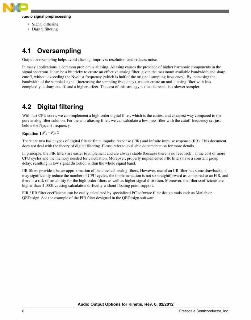
FIR / IIR filter coefficients can be easily calculated by specialized PC software filter design tools such as Matlab orQEDesign. See the example of the FIR filter designed in the QEDesign software.
Audio signal preprocessing
Audio Output Options for Kinetis, Rev. 0, 02/2012
6 Freescale Semiconductor, Inc.
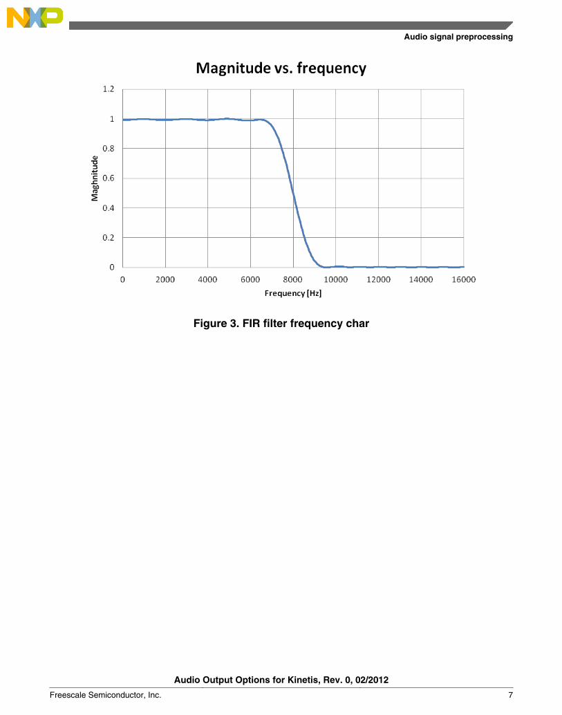
Figure 3. FIR filter frequency char
Audio signal preprocessing
Audio Output Options for Kinetis, Rev. 0, 02/2012
Freescale Semiconductor, Inc. 7
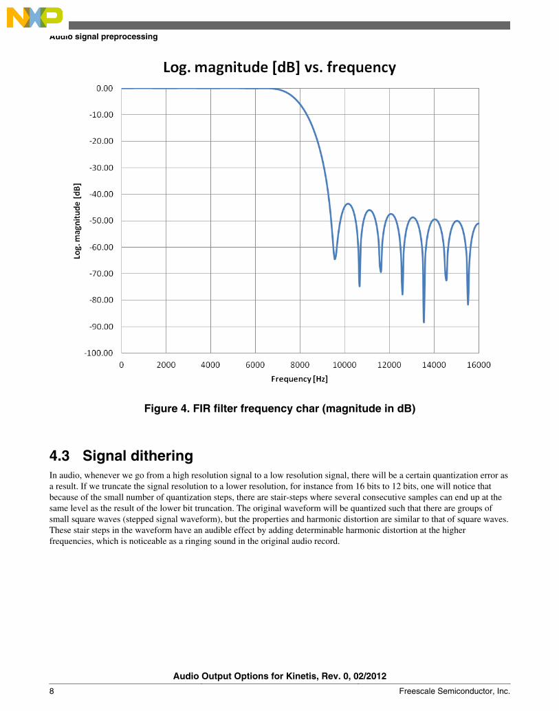
Figure 4. FIR filter frequency char (magnitude in dB)
4.3 Signal ditheringIn audio, whenever we go from a high resolution signal to a low resolution signal, there will be a certain quantization error asa result. If we truncate the signal resolution to a lower resolution, for instance from 16 bits to 12 bits, one will notice thatbecause of the small number of quantization steps, there are stair-steps where several consecutive samples can end up at thesame level as the result of the lower bit truncation. The original waveform will be quantized such that there are groups ofsmall square waves (stepped signal waveform), but the properties and harmonic distortion are similar to that of square waves.These stair steps in the waveform have an audible effect by adding determinable harmonic distortion at the higherfrequencies, which is noticeable as a ringing sound in the original audio record.
Audio signal preprocessing
Audio Output Options for Kinetis, Rev. 0, 02/2012
8 Freescale Semiconductor, Inc.
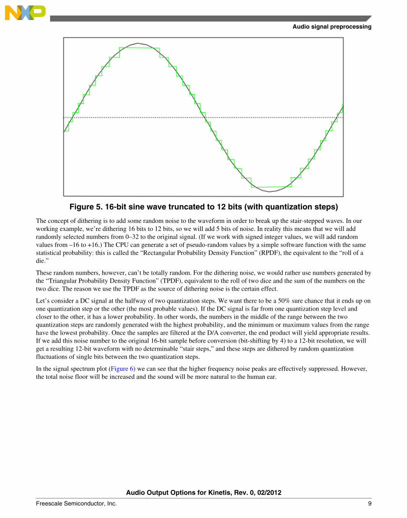
Figure 5. 16-bit sine wave truncated to 12 bits (with quantization steps)
The concept of dithering is to add some random noise to the waveform in order to break up the stair-stepped waves. In ourworking example, we’re dithering 16 bits to 12 bits, so we will add 5 bits of noise. In reality this means that we will addrandomly selected numbers from 0–32 to the original signal. (If we work with signed integer values, we will add randomvalues from –16 to +16.) The CPU can generate a set of pseudo-random values by a simple software function with the samestatistical probability: this is called the “Rectangular Probability Density Function” (RPDF), the equivalent to the “roll of adie.”
These random numbers, however, can’t be totally random. For the dithering noise, we would rather use numbers generated bythe “Triangular Probability Density Function” (TPDF), equivalent to the roll of two dice and the sum of the numbers on thetwo dice. The reason we use the TPDF as the source of dithering noise is the certain effect.
Let’s consider a DC signal at the halfway of two quantization steps. We want there to be a 50% sure chance that it ends up onone quantization step or the other (the most probable values). If the DC signal is far from one quantization step level andcloser to the other, it has a lower probability. In other words, the numbers in the middle of the range between the twoquantization steps are randomly generated with the highest probability, and the minimum or maximum values from the rangehave the lowest probability. Once the samples are filtered at the D/A converter, the end product will yield appropriate results.If we add this noise number to the original 16-bit sample before conversion (bit-shifting by 4) to a 12-bit resolution, we willget a resulting 12-bit waveform with no determinable “stair steps,” and these steps are dithered by random quantizationfluctuations of single bits between the two quantization steps.
In the signal spectrum plot (Figure 6) we can see that the higher frequency noise peaks are effectively suppressed. However,the total noise floor will be increased and the sound will be more natural to the human ear.
Audio signal preprocessing
Audio Output Options for Kinetis, Rev. 0, 02/2012
Freescale Semiconductor, Inc. 9
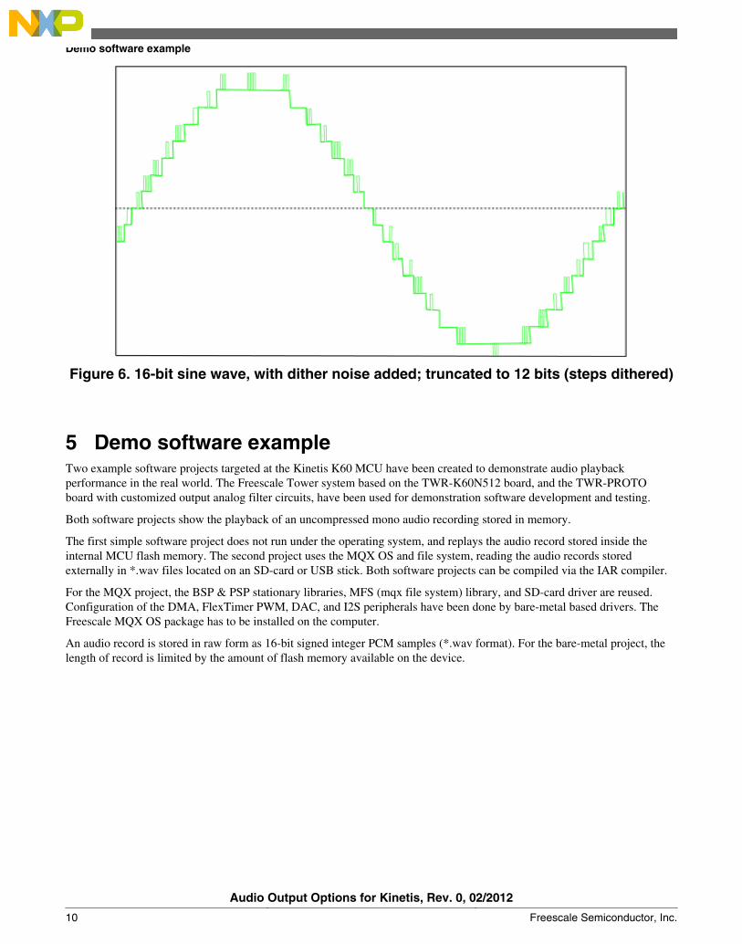
Figure 6. 16-bit sine wave, with dither noise added; truncated to 12 bits (steps dithered)
5 Demo software exampleTwo example software projects targeted at the Kinetis K60 MCU have been created to demonstrate audio playbackperformance in the real world. The Freescale Tower system based on the TWR-K60N512 board, and the TWR-PROTOboard with customized output analog filter circuits, have been used for demonstration software development and testing.
Both software projects show the playback of an uncompressed mono audio recording stored in memory.
The first simple software project does not run under the operating system, and replays the audio record stored inside theinternal MCU flash memory. The second project uses the MQX OS and file system, reading the audio records storedexternally in *.wav files located on an SD-card or USB stick. Both software projects can be compiled via the IAR compiler.
For the MQX project, the BSP & PSP stationary libraries, MFS (mqx file system) library, and SD-card driver are reused.Configuration of the DMA, FlexTimer PWM, DAC, and I2S peripherals have been done by bare-metal based drivers. TheFreescale MQX OS package has to be installed on the computer.
An audio record is stored in raw form as 16-bit signed integer PCM samples (*.wav format). For the bare-metal project, thelength of record is limited by the amount of flash memory available on the device.
Demo software example
Audio Output Options for Kinetis, Rev. 0, 02/2012
10 Freescale Semiconductor, Inc.
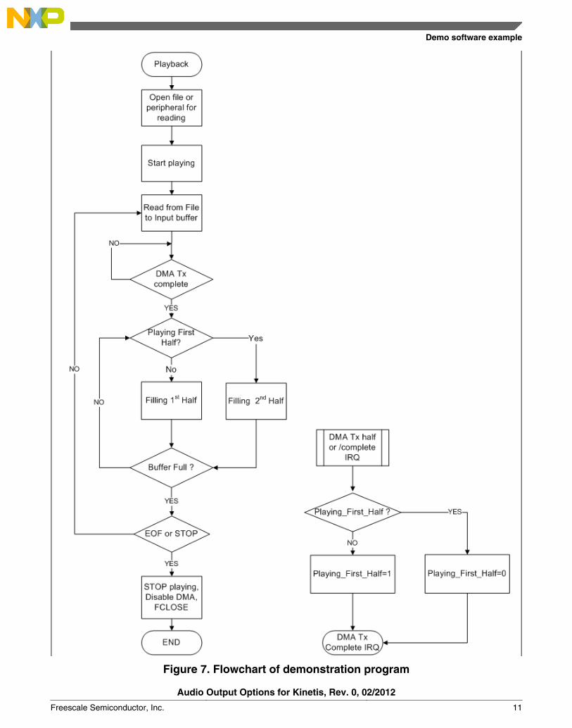
Figure 7. Flowchart of demonstration program
Demo software example
Audio Output Options for Kinetis, Rev. 0, 02/2012
Freescale Semiconductor, Inc. 11
6 Audio output hardware considerationsAs mentioned above, for the PWM output, we can use a simple RC filter for reconstruction of the PCM samples. PWMoutput can provide enough current for driving low-impedance headphones, or an external amplifier input, directly.
6.1 PWM hardware outputThe PWM output signal from the FlexTimer output is fed to a simple low-pass RC filter to generate an output voltage. Theoutput voltage is proportional to the average time spent in the High state (a 50% duty cycle is equal to one half of themaximum output voltage, in other words 1.65 V when VDD = 3.3 V). When this is averaged over time, we can reconstructthe original analog signal.
The cutoff frequency has to be set equal to, or just under, the Nyquist frequency, which will additionally suppress theunwanted high frequency noise. Since the application can support different sample rates (8000/11025/16000/22050/44100),we must take into consideration the bandwidth limitation caused by the lower sample rates. A higher PWM frequency can befiltered more easily, but the PWM resolution may be limited.
For instance: if the original signal sampling frequency is 8 kHz, the filter cutoff frequency has to be set to 4 kHz. Thisensures that almost the entire audio spectrum is passed through, but the PWM switching frequency and noise is filtered.
These formulae are valid for the RC filter component values:
Equation 2:
Equation 3:
Where ‘f’ is the filter cut-off frequency.
In our example (f = 4 kHz), the R = 1.2kΩ and C = 33nF
See the example of a filtered sine wave (500Hz) generated by PWM output and filtered.
Audio output hardware considerations
Audio Output Options for Kinetis, Rev. 0, 02/2012
12 Freescale Semiconductor, Inc.
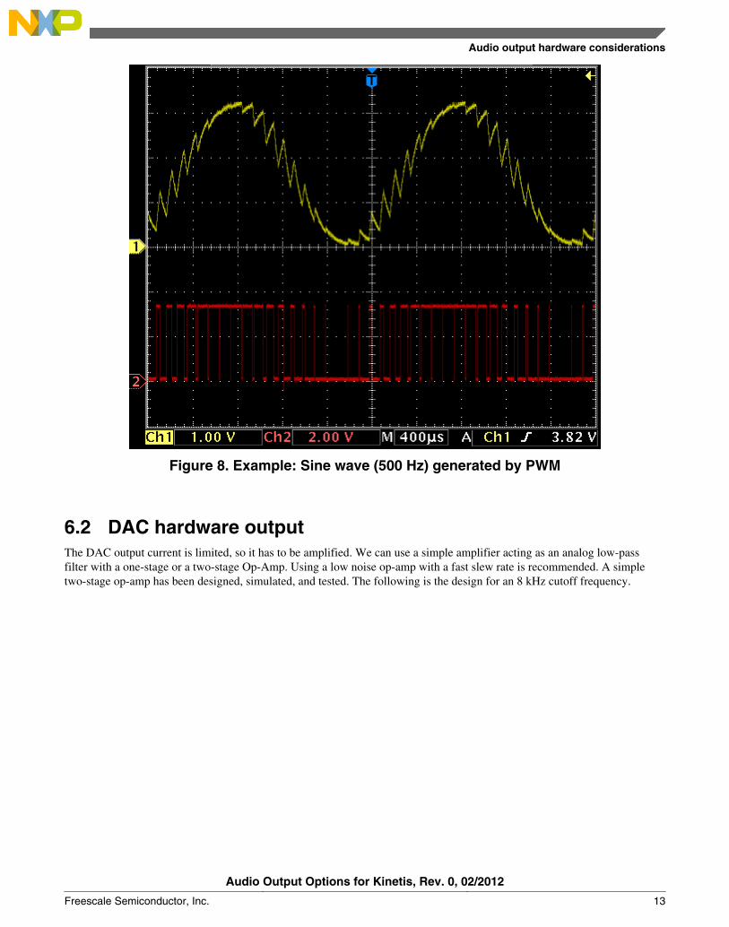
Figure 8. Example: Sine wave (500 Hz) generated by PWM
6.2 DAC hardware outputThe DAC output current is limited, so it has to be amplified. We can use a simple amplifier acting as an analog low-passfilter with a one-stage or a two-stage Op-Amp. Using a low noise op-amp with a fast slew rate is recommended. A simpletwo-stage op-amp has been designed, simulated, and tested. The following is the design for an 8 kHz cutoff frequency.
Audio output hardware considerations
Audio Output Options for Kinetis, Rev. 0, 02/2012
Freescale Semiconductor, Inc. 13
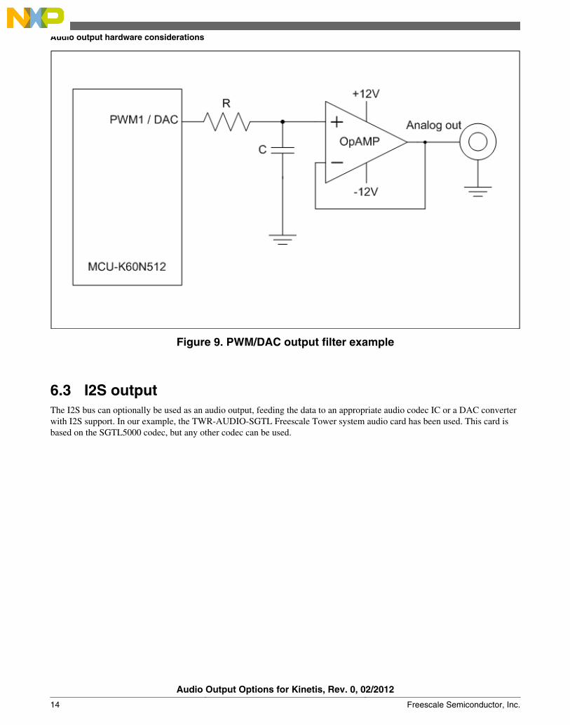
Figure 9. PWM/DAC output filter example
6.3 I2S outputThe I2S bus can optionally be used as an audio output, feeding the data to an appropriate audio codec IC or a DAC converterwith I2S support. In our example, the TWR-AUDIO-SGTL Freescale Tower system audio card has been used. This card isbased on the SGTL5000 codec, but any other codec can be used.
Audio output hardware considerations
Audio Output Options for Kinetis, Rev. 0, 02/2012
14 Freescale Semiconductor, Inc.
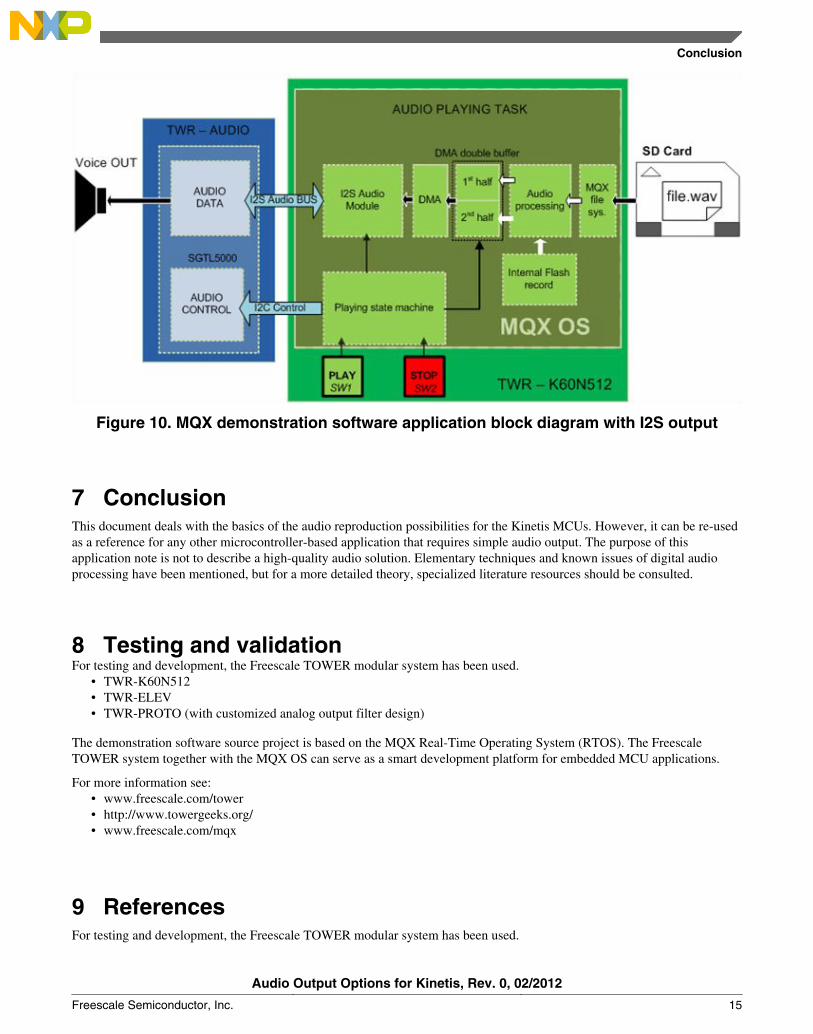
Figure 10. MQX demonstration software application block diagram with I2S output
7 ConclusionThis document deals with the basics of the audio reproduction possibilities for the Kinetis MCUs. However, it can be re-usedas a reference for any other microcontroller-based application that requires simple audio output. The purpose of thisapplication note is not to describe a high-quality audio solution. Elementary techniques and known issues of digital audioprocessing have been mentioned, but for a more detailed theory, specialized literature resources should be consulted.
8 Testing and validationFor testing and development, the Freescale TOWER modular system has been used.
• TWR-K60N512• TWR-ELEV• TWR-PROTO (with customized analog output filter design)
The demonstration software source project is based on the MQX Real-Time Operating System (RTOS). The FreescaleTOWER system together with the MQX OS can serve as a smart development platform for embedded MCU applications.
For more information see:• www.freescale.com/tower• http://www.towergeeks.org/• www.freescale.com/mqx
9 ReferencesFor testing and development, the Freescale TOWER modular system has been used.
Conclusion
Audio Output Options for Kinetis, Rev. 0, 02/2012
Freescale Semiconductor, Inc. 15
1. Aldrich, Nika (2002, April 25). "Dither Explained: An explanation and proof of the benefit of dither for the audioengineer." Version 5.5.02. [downloaded 2011-12-05]. Retrieved from the web site: http://www.users.qwest.net/~volt42/cadenzarecording/DitherExplained.pdf
2. Steepest Ascent (2006). DSPedia. Introduction to DSP, Version 4.4/9/07. http://www.steepestascent.com
References
Audio Output Options for Kinetis, Rev. 0, 02/2012
16 Freescale Semiconductor, Inc.
How to Reach Us:
Home Page:www.freescale.com
Web Support:http://www.freescale.com/support
USA/Europe or Locations Not Listed:Freescale SemiconductorTechnical Information Center, EL5162100 East Elliot RoadTempe, Arizona 85284+1-800-521-6274 or +1-480-768-2130www.freescale.com/support
Europe, Middle East, and Africa:Freescale Halbleiter Deutschland GmbHTechnical Information CenterSchatzbogen 781829 Muenchen, Germany+44 1296 380 456 (English)+46 8 52200080 (English)+49 89 92103 559 (German)+33 1 69 35 48 48 (French)www.freescale.com/support
Japan:Freescale Semiconductor Japan Ltd.HeadquartersARCO Tower 15F1-8-1, Shimo-Meguro, Meguro-ku,Tokyo 153-0064Japan0120 191014 or +81 3 5437 [email protected]
Asia/Pacific:Freescale Semiconductor China Ltd.Exchange Building 23FNo. 118 Jianguo RoadChaoyang DistrictBeijing 100022China+86 10 5879 [email protected]
Document Number: AN4369Rev. 0, 02/2012
Information in this document is provided solely to enable system and softwareimplementers to use Freescale Semiconductors products. There are no express or impliedcopyright licenses granted hereunder to design or fabricate any integrated circuits orintegrated circuits based on the information in this document.
Freescale Semiconductor reserves the right to make changes without further notice to anyproducts herein. Freescale Semiconductor makes no warranty, representation, orguarantee regarding the suitability of its products for any particular purpose, nor doesFreescale Semiconductor assume any liability arising out of the application or use of anyproduct or circuit, and specifically disclaims any liability, including without limitationconsequential or incidental damages. "Typical" parameters that may be provided inFreescale Semiconductor data sheets and/or specifications can and do vary in differentapplications and actual performance may vary over time. All operating parameters,including "Typicals", must be validated for each customer application by customer'stechnical experts. Freescale Semiconductor does not convey any license under its patentrights nor the rights of others. Freescale Semiconductor products are not designed,intended, or authorized for use as components in systems intended for surgical implantinto the body, or other applications intended to support or sustain life, or for any otherapplication in which failure of the Freescale Semiconductor product could create asituation where personal injury or death may occur. Should Buyer purchase or useFreescale Semiconductor products for any such unintended or unauthorized application,Buyer shall indemnify Freescale Semiconductor and its officers, employees, subsidiaries,affiliates, and distributors harmless against all claims, costs, damages, and expenses, andreasonable attorney fees arising out of, directly or indirectly, any claim of personal injuryor death associated with such unintended or unauthorized use, even if such claims allegesthat Freescale Semiconductor was negligent regarding the design or manufacture ofthe part.
RoHS-compliant and/or Pb-free versions of Freescale products have the functionality andelectrical characteristics as their non-RoHS-complaint and/or non-Pb-free counterparts.For further information, see http://www.freescale.com or contact your Freescalesales representative.
For information on Freescale's Environmental Products program, go tohttp://www.freescale.com/epp.
Freescale™ and the Freescale logo are trademarks of Freescale Semiconductor, Inc.All other product or service names are the property of their respective owners.
© 2012 Freescale Semiconductor, Inc.