Embed Size (px)
Citation preview
January 13, 2017 © 2017 Transphorm Inc. Subject to change without notice.
an0008.3 1
Application Note 0008
Drain Voltage and Avalanche Ratings for GaN FETs
Abstract This application note compares a silicon MOSFET’s avalanche rating and Transphorm’s GaN FET transient drain-to-source
(“VTDS”) rating.
Table of Contents
Introduction .......................................................................................................................................................................................... 2
Drain Voltage Stress and Avalanche .................................................................................................................................................. 2
Testing GaN FET Max VDS .................................................................................................................................................................... 6
Conclusion ............................................................................................................................................................................................ 6
Bibliography ......................................................................................................................................................................................... 6
January 13, 2017 transphormusa.com
an0008.3 2
Application Note 0008
Introduction Many customers have asked if Transphorm’s GaN FETs have an avalanche rating. This note explains that, unlike traditional
vertical silicon MOSFETs, Transphorm’s lateral GaN FETs do not have a body diode and therefore no physical avalanche
mechanism. GaN FETs do have a dielectric breakdown voltage, similar to that of capacitors, which is often as much as three
times higher than their datasheet maximum voltage rating. To confirm reliability, one of the several tests Transphorm performs
on its 650V-rated GaN FETs is the High Voltage Off State (HVOS), which applies as high as 1150V1 for extended periods. One of
the major advantages of GaN FETs is that they do not have this lossy high capacitance body diode. The absence of this parasitic
body diode allows GaN FETs to be used in new topologies and to attain higher levels of efficiency in power conversion
applications than is possible with silicon FETs. Instead of an avalanche voltage rating, which should never be exceeded in
traditional high-voltage silicon MOSFETs due to reliability concerns, Transphorm’s GaN devices are rated for a transient peak
voltage that is ~25% higher (e.g. 800V for a 650V part) than the continuous rating. This peak transient rating is significantly
below voltage levels that could result in device failures.
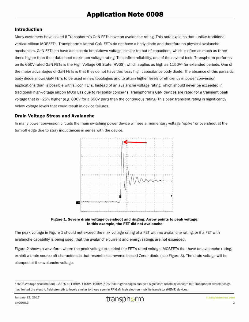
Drain Voltage Stress and Avalanche In many power conversion circuits the main switching power device will see a momentary voltage “spike” or overshoot at the
turn-off edge due to stray inductances in series with the device.
Figure 1. Severe drain voltage overshoot and ringing. Arrow points to peak voltage. In this example, the FET did not avalanche
The peak voltage in Figure 1 should not exceed the max voltage rating of a FET with no avalanche rating; or if a FET with
avalanche capability is being used, that the avalanche current and energy ratings are not exceeded.
Figure 2 shows a waveform where the peak voltage exceeded the FET’s rated voltage. MOSFETs that have an avalanche rating,
exhibit a drain-source off characteristic that resembles a reverse-biased Zener diode (see Figure 3). The drain voltage will be
clamped at the avalanche voltage.
1 HVOS (voltage acceleration) – 82°C at 1150V, 1100V, 1050V (50% fail): High voltages can be a significant reliability concern but Transphorm device design
has limited the electric field strength to levels similar to those seen in RF GaN high electron mobility transistor (HEMT) devices.
January 13, 2017 transphormusa.com
an0008.3 3
Application Note 0008
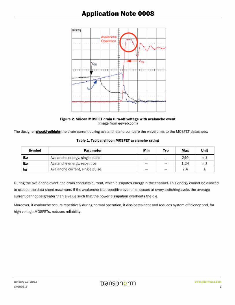
Figure 2. Silicon MOSFET drain turn-off voltage with avalanche event (image from eeweb.com)
The designer should validate the drain current during avalanche and compare the waveforms to the MOSFET datasheet:
Table 1. Typical silicon MOSFET avalanche rating
Symbol Parameter Min Typ Max Unit
EAS Avalanche energy, single pulse — — 249 mJ EAR Avalanche energy, repetitive — — 1.24 mJ IAS Avalanche current, single pulse — — 7.4 A
During the avalanche event, the drain conducts current, which dissipates energy in the channel. This energy cannot be allowed
to exceed the data sheet maximum. If the avalanche is a repetitive event, i.e. occurs at every switching cycle, the average
current cannot be greater than a value such that the power dissipation overheats the die.
Moreover, if avalanche occurs repetitively during normal operation, it dissipates heat and reduces system efficiency and, for
high voltage MOSFETs, reduces reliability.
January 13, 2017 transphormusa.com
an0008.3 4
Application Note 0008
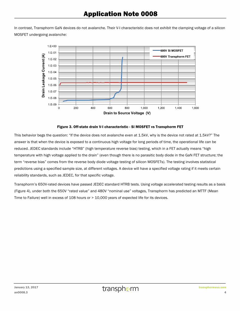
In contrast, Transphorm GaN devices do not avalanche. Their V-I characteristic does not exhibit the clamping voltage of a silicon
MOSFET undergoing avalanche:
Figure 3. Off-state drain V-I characteristic - Si MOSFET vs Transphorm FET
This behavior begs the question: “If the device does not avalanche even at 1.5kV, why is the device not rated at 1.5kV?” The
answer is that when the device is exposed to a continuous high voltage for long periods of time, the operational life can be
reduced. JEDEC standards include “HTRB” (high temperature reverse bias) testing, which in a FET actually means “high
temperature with high voltage applied to the drain” (even though there is no parasitic body diode in the GaN FET structure; the
term “reverse bias” comes from the reverse body diode voltage testing of silicon MOSFETs). The testing involves statistical
predictions using a specified sample size, at different voltages. A device will have a specified voltage rating if it meets certain
reliability standards, such as JEDEC, for that specific voltage.
Transphorm’s 650V-rated devices have passed JEDEC standard HTRB tests. Using voltage accelerated testing results as a basis
(Figure 4), under both the 650V “rated value” and 480V “nominal use” voltages, Transphorm has predicted an MTTF (Mean
Time to Failure) well in excess of 108 hours or > 10,000 years of expected life for its devices.
January 13, 2017 transphormusa.com
an0008.3 5
Application Note 0008
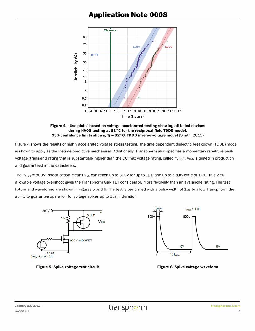
Figure 4. “Use-plots” based on voltage-accelerated testing showing all failed devices during HVOS testing at 82°C for the reciprocal field TDDB model.
99% confidence limits shown, Tj = 82°C, TDDB inverse voltage model (Smith, 2015)
Figure 4 shows the results of highly accelerated voltage stress testing. The time dependent dielectric breakdown (TDDB) model
is shown to apply as the lifetime predictive mechanism. Additionally, Transphorm also specifies a momentary repetitive peak
voltage (transient) rating that is substantially higher than the DC max voltage rating, called “VTDS”. VTDS is tested in production
and guaranteed in the datasheets.
The “VTDS = 800V” specification means VDS can reach up to 800V for up to 1µs, and up to a duty cycle of 10%. This 23%
allowable voltage overshoot gives the Transphorm GaN FET considerably more flexibility than an avalanche rating. The test
fixture and waveforms are shown in Figures 5 and 6. The test is performed with a pulse width of 1µs to allow Transphorm the
ability to guarantee operation for voltage spikes up to 1µs in duration.
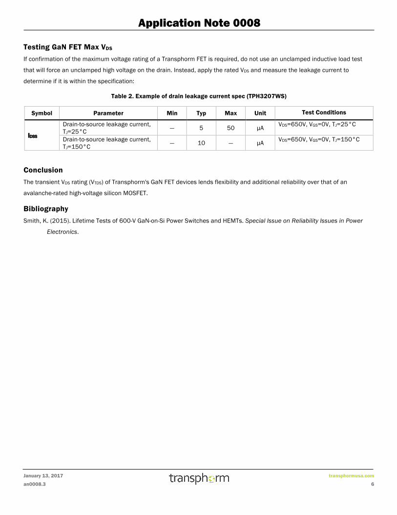
Figure 5. Spike voltage test circuit
Figure 6. Spike voltage waveform
January 13, 2017 transphormusa.com
an0008.3 6
Application Note 0008
Testing GaN FET Max VDS If confirmation of the maximum voltage rating of a Transphorm FET is required, do not use an unclamped inductive load test
that will force an unclamped high voltage on the drain. Instead, apply the rated VDS and measure the leakage current to
determine if it is within the specification:
Table 2. Example of drain leakage current spec (TPH3207WS)
Symbol Parameter Min Typ Max Unit Test Conditions
IDSS
Drain-to-source leakage current, TJ=25°C — 5 50 µA VDS=650V, VGS=0V, TJ=25°C
Drain-to-source leakage current, TJ=150°C — 10 — µA VDS=650V, VGS=0V, TJ=150°C
Conclusion The transient VDS rating (VTDS) of Transphorm's GaN FET devices lends flexibility and additional reliability over that of an
avalanche-rated high-voltage silicon MOSFET.
Bibliography Smith, K. (2015). Lifetime Tests of 600-V GaN-on-Si Power Switches and HEMTs. Special Issue on Reliability Issues in Power
Electronics.