Embed Size (px)
Citation preview

1 Revision 1.1, 2015-05-12
About this document
Scope and purpose
This application note describes the characteristics and features of 650 V CoolMOS™ C6 and E6 and how it
differentiates from earlier CoolMOS™ technology. In addition, key parameters of the device which are critical in achieving the desired efficiency and reliability of the application are discussed in details. Moreover, the
evaluation result in PFC stage application is also presented to provide an overview of the efficiency benefit of CoolMOS™ C6 and E6.
Intended audience
This document provides designers a guideline on how to use the device in a wide array of applications from
low to high power to attain an efficient and robust solution with minimum design effort and improved
overall cost.
Table of Contents
1 Introduction ................................................................................................................................... 2
2 Technology Characteristics of CoolMOS™ C6 and E6 650V ............................................................. 3
2.1 Key Parameters ................................................................................................................................... 3 2.2 The difference between CoolMOS™ C6 and E6: Integrated Gate Resistor ........................................ 4 2.3 Switching Characteristics ................................................................................................................... 5
2.3.1 Switching Speed ............................................................................................................................ 5 2.3.2 Switching Waveforms and Noise Considerations ........................................................................ 6
2.4 Device Capacitances ........................................................................................................................... 8 2.5 Behavior during hard commutation of the body diode ..................................................................... 8
3 Application Results ........................................................................................................................ 9 3.1 PFC stage of a 300W Power Supply ................................................................................................... 10
4 Product Portfolio and Naming System ......................................................................................... 11
650 V CoolMOS™ C6/ E6
Fe atur es a nd Be ne fi t s o f 6 50 V Coo lMOS ™
C6 / E6
Application Note

Features and Benefits of 650V CoolMOS™ C6/E6
Introduction
Application Note 2 Revision 1.11, 2015-05-12
1 Introduction With fifth Superjunction generation CoolMOS™ C6 Infineon Technologies has set a standard in the market for
high voltage MOSFETs. After launching the 600 V class in 2009, C6 technology is now also available in 650 V. CoolMOS™ C6 technology implements a combination of ultra-low RDS(on), high ruggedness and fast but well
controlled switching speed. The application measurements show very good light load efficiency in
comparison to our own devices and competitor parts, a fault tolerant behavior in abnormal conditions such as turn-on on a conducting body diode and a well controlled switching characteristic especially in peak
current conditions such as load steps, start-up and AC cycle drop out etc. Last but not least the cost associated with the production of a given RDS(on) was reduced, allowing us to offer lower prices compared to
previous CoolMOS™ generations.
CoolMOS™ C6 comes with an integrated gate resistor in order to achieve self-limiting di/dt and dv/dt
characteristics. This is especially important for consumer applications such as adapters for notebooks and
printers, where easy implementation and lowest noise levels are key requirements.
To allow for maximum flexibility in design-in, the technology platform is also offered with reduced
integrated gate resistor for a part of the offered RDS(on) range, promoted as CoolMOS™ E6 series. This we
consider particularly important for applications where highest efficiency and power density are key
requirements.
In summary, the combination of 650 V CoolMOS™ C6 and E6 series is capable to fulfill the needs of a very
wide range of applications comprising fields such as computing, lighting, industrial, and consumer.
This document is particularly showing results of application measurements and application relevant
measurements for 650 V CoolMOS™ C6 and E6 in comparison to 650 V CoolMOS™ C3.
For a general introduction of the CoolMOS™ C6 technology together with a comparison to other CoolMOS
technologies, please refer to the application note CoolMOS™ C6 - Mastering the Art of Slowness available on our homepage.
Features and Benefits of 650V CoolMOS™ C6/E6
Technology Characteristics of CoolMOS™ C6 and E6 650V
Application Note 3 Revision 1.11, 2015-05-12
2 Technology Characteristics of CoolMOS™ C6 and E6 650V CoolMOS™ C6 and E6 products are well balanced modern Superjunction high-voltage MOSFETs with the following characteristics:
Fast but well controlled switching speed
Very low energy stored in output capacitance
High ruggedness in hard commutation of the body diode
Low gate current requirements
This gives the application benefits like:
Compact and very efficient designs
Fast and easy design-in, less care for peak current conditions such as during start-up, load jump, AC cycle
drop out etc.
Very good light load efficiency in hard turn on applications
If low Qrr is not key requirement, no need for more expensive fast body diode types
No need for high current gate drivers, better system cost and more choice
2.1 Key Parameters
Table 1 shows a comparison of key characteristics as published in the datasheet.
Table 1 Key feature comparison of CoolMOS™ C3 versus C6 and E6 series
Specification Symbol SPP15N65C3 IPP65R280C6 IPP65R280E6
On-state resistance, maximum
rating, 25 C RDS(on) 280 m 280 m 280 m
Drain current rating ID 15 A 13.8 A 13.8 A
Pulse current rating ID,pulse 45 A 39 A 39 A
Typical Gate - Drain charge Qgd 29 nC 24 nC 24nC
Total Gate charge Qg 63 nC 45 nC 45 nC
Energy stored in output capacitance @400V
EOSS 5.7 µJ 3.7 J 3.7 J
Thermal resistance, junction-case RthJC,max 0.8 K/W 1.2 K/W 1.2 K/W
Body diode, reverse recovery charge
Qrr 8 µC 3.6 µC 3.6 µC
Body diode, di/dt diF/dt 400 A/µs1 500 A/µs 500 A/µs
Body diode, dv/dt dv/dt 15 V/ns1 15 V/ns 15 V/ns
Gate resistance RG 1.4 12.5 7.0
The target for CoolMOS™ C6 is to provide fast but controlled switching and a good compatibility with layouts, where source inductances have not been brought to the absolute minimum. The basic idea is to provide a high voltage MOSFET, which is significantly fast at normal operation conditions and very limited
1 Not specified in datasheet
Features and Benefits of 650V CoolMOS™ C6/E6
Technology Characteristics of CoolMOS™ C6 and E6 650V
Application Note 4 Revision 1.11, 2015-05-12
overshoot in di/dt or dv/dt at high peak current conditions. With its outstanding behavior during hard commutation of the body diode CoolMOS™ C6 and E6 is very well suited for resonant applications.
2.2 The difference between CoolMOS™ C6 and E6: Integrated Gate Resistor
CoolMOS™ C6 comes with an integrated gate resistor in order to achieve self-limiting di/dt and dv/dt characteristics. This integrated RG allows fast turn on and turn off at normal operating current conditions
but limits the di/dt and dv/dt in case of peak current conditions. The values of integrated RG scales inversely
with the gate charge respectively device capacitances.
A part of the portfolio is available with reduced integrated gate resistor in order to support applications where highest efficiency and power density are key requirements. These devices represent the CoolMOS™ E6
series.
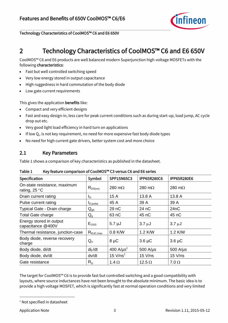
The following values have been chosen for CoolMOS™ C6 and E6 series:
Type C6 RG [Ω] E6 RG [Ω]
IPx65R600x6 17.5 10.5
IPx65R380x6 17.0 7.5
IPx65R280x6 12.5 7.0
IPx65R190x6 8.5 6.0
Figure 1 Integrated Gate resistor for CoolMOS™ C6 versus E6 series
Please note that the C6 devices with RDS(on) values below 99 m come with very low integrated gate resistances. Low RDS(on) values require larger silicon area and thus exhibit larger device capacitances. For those parts it is not necessary additionally limit the di/dt and dv/dt values. Low ohmic C6 parts are therefore
ideally suited for applications with highest efficiency requirements, like e.g. solar inverters.
Due to low gate charge plus integrated gate resistors the gate current is relatively low; hence the use of low
cost gate drivers is possible. In case of e.g. the 190 mΩ C6 part the 8.5 Ω integrated RG limits the gate current to less than 2A even when switching with 0 Ω external RG from 0 to 15 V. During the Miller phase the gate
current will typically be even less than 1 A. In combination with a relatively low total gate charge the losses
dissipated in the driver are considerably lower as well.
We encourage using very small external gate resistors especially for the C6 technology to achieve optimum efficiency across a wide range of load conditions.
0
2
4
6
8
10
12
14
16
18
20
0 100 200 300 400 500 600 700
Rdson [mOhm]
inte
gra
ted
Rg
[O
hm
]
C6
E6

Features and Benefits of 650V CoolMOS™ C6/E6
Technology Characteristics of CoolMOS™ C6 and E6 650V
Application Note 5 Revision 1.11, 2015-05-12
2.3 Switching Characteristics
2.3.1 Switching Speed
Figure 1 and Figure 2 show a technology comparison of C3 versus C6 and E6 for di/dt and dv/dt both during
turn on and turn off at currents of 3.3 A and 13.8 A respectively. All measured parts have a maximum on-
state resistance of 280 m, the used gate resistance is 3.4 .
Figure 2 Comparison of switching characteristic, di/dt at turn on and turn off for 3.3 A and 13.8 A
respectively, 280 m types, RG=3.4 , VG=13 V, Tj=125°C
Figure 3 Comparison of switching characteristic, dv/dt at turn on and turn off for 3.3 A and 13.8 A
respectively, 280 m types, RG=3.4 , VG=13 V, Tj=125°C
0
500
1000
1500
2000
2500
3000
3500
4000
4500
dI/d
t_on
3.3
A
dI/d
t_on
13.
8A
dI/d
t_of
f 3.3
A
dI/d
t_of
f 13.
8A
dId
/dt
[A/µ
s]
C6 E6 C3
0
20
40
60
80
100
120
dV/d
t_on
3.3
A
dV/d
t_on
13.
8A
dV/d
t_of
f 3.3
A
dV/d
t_of
f 13.
8A
dV
ds
/dt
[V/n
s]
C6 E6 C3

Features and Benefits of 650V CoolMOS™ C6/E6
Technology Characteristics of CoolMOS™ C6 and E6 650V
Application Note 6 Revision 1.11, 2015-05-12
Figure 2 and Figure 3 show di/dt and dv/dt results of a measurement with very low gate resistance at normal operating currents as well as high currents (even above nominal DC current) to demonstrate the nicely
controlled switching behavior even under non-standard operating conditions.
CoolMOS™ C6 and E6 show relatively low values of di/dt during turn off. During turn-on di/dt values are significantly lower than for CoolMOS™ C3. For C6 and E6 there is no increase in di/dt during turn on (in this measurement even a decrease of di/dt for higher currents was detected) and only an increase to moderate
values in di/dt during turn off when the current changes from 3.3 A to 13.8 A. This enhances design safety in peak current conditions such as AC cycle drop out, start up or load jumps as the di/dt is likely above the range of normal operation conditions. Therefore the likelihood of unwanted oscillations or dangerous gate spikes is significantly suppressed.
For those who might consider the di/dt values at turn off rather low, please remember that di/dt values of
500 A/µs and a source inductance of 10 nH only will already yield a voltage drop of 5 V, which will bring the MOSFET already for short time into the Miller plateau via inductively induced turn on. As both the TO-220
and TO-247 package have parasitic source inductances of 5nH already there is little room for layout routing to stay below 10 nH. In other words with conventional packages such as TO-220 or TO-247 there is little to no
benefit from higher switching speeds than 800 to 1000 A/µs. The self limitation of di/dt being implemented in CoolMOS™ C6 and E6 does therefore not hurt efficiency wise but brings safety in peak current conditions
and helps with the use of the part in non-ideal layout environments.
Looking at dv/dt, the device is able to achieve very fast turn on and turn off transients to provide low turn on
and turn off losses. At high currents (peak current conditions) the dv/dt values are limited compared to C3, allowing to stay within the datasheet specification with comparably low external RG values and thus not
reducing switching speed in normal operating conditions. The dv/dt values are in general close to what
CoolMOS™ C3 would yield under identical conditions, thus facilitating the change of designs from C3 into
C6/E6 to participate in the best-in-class offerings, improved EOSS and gate charge characteristics and last but
not least attractive price structure of the more modern CoolMOS™ class. Furthermore CoolMOS™ C6 and E6
do not show extremely high dv/dt values at turn off under peak current conditions, as untamed
Superjunction devices naturally tend to do due to ever decreasing output capacitance. The device offers therefore well controlled switching behavior with significantly suppressed tendency to unwanted ringing
and gate spikes.
Figure 2 and Figure 3 clearly demonstrate the design-in flexibility that is offered with the additional E6 series
which is offered with reduced integrated gate resistor, allowing for highest efficiency and power density. Customers are able to choose the device that matches their optimum trade-off between lowest losses and
ease of use.
2.3.2 Switching Waveforms and Noise Considerations
In Figure 4 the measured switching waveforms of the device are shown for a typical PFC stage exhibiting
7.2 pF capacitive coupling between gate and drain on the PCB circuit. This parasitic capacitance can be the source for noise on the switching waveforms. In new layouts designers should take care to minimize this external gate to drain capacitance to enable highest performance of MOSFETs. Gate waveforms (in
magenta) are shown for increasing drain current (in turquoise). Conditions applied at the device are VDS=400 V (shown in green) and VG=15 V. The current is increased during every pulse up to saturation current.
All devices were measured with an external gate resistance of only 0.5 , to visualize the clear difference of switching behavior between devices. The magnified waveform shows the gate turn-on of the last pulse before saturation, i.e. at very high currents of up to 60 A. C6, with the highest integrated RG, shows an
excellent switching waveform, no gate spikes are visible up to four times nominal current. The noise level to be expected from CoolMOS™ C6 also in terms of EMI can be expected to be very low. Also the variant with

Features and Benefits of 650V CoolMOS™ C6/E6
Technology Characteristics of CoolMOS™ C6 and E6 650V
Application Note 7 Revision 1.11, 2015-05-12
reduced internal gate resistance, CoolMOS™ E6, shows very good switching waveforms, with even lower noise level than the previous generation CoolMOS™ C3.
Figure 4 Measured switching waveforms during current ramp up in a CCM PFC stage exhibiting a Cgd,ext of
7.2 pF for 380m devices of CoolMOS™ C3, C6 and E6 with RG,ext=0.5
The waveforms show that the integration of a high enough gate resistance allows to easily design-in modern
superjunction devices in applications that have high parasitics inherent to the layout. This way the benefit of lowest device capacitances can be fully used without sacrificing ease of use of the device.
In order not to sacrifice efficiency, please make sure the external gate resistance is reduced compared to previously used MOSFETs (please refer to table 2 for internal RG values).
Despite all measures taken from a device design point of view to suppress gate spikes Infineon Technologies
recommends the layout suggestions and gate driver setup as e.g. described in the application note CoolMOS™ CP. The use of ferrite beads on the gate is generally recommended for paralleled devices.
IPA65R380C6
IPA65R380E6
SPA11N65C3
ID VG
VDS
VG
ID VG
VDS
VG
ID VG
VDS
VG

Features and Benefits of 650V CoolMOS™ C6/E6
Technology Characteristics of CoolMOS™ C6 and E6 650V
Application Note 8 Revision 1.11, 2015-05-12
2.4 Device Capacitances,
Figure 5 Figure 5: Comparison of the energy stored in the output capacitance EOSS and the capacitive
displacement charge QOSS for CoolMOS™ C3 versus C6 and E6, RDS(on),max=280 m
Figure 5 shows a comparison of the energy stored in the output capacitance EOSS and the capacitive
displacement charge Qoss as a function of the voltage the device is charged up to. As it can be clearly seen
from the graph the new CoolMOS™ generations C6 and E6 shows the best EOSS values at 400 V, which helps to
lower the capacitive losses in applications with hard turn on such as continues current mode PFC applications. As the capacitive losses are load independent these loss contribution typically dominates
during light load conditions, when both conduction and Joule switching losses get lower due to their square or linear relationship with load current respectively. At 200 V the Eoss curve of C6 intersects with C3 yielding
similar capacitive losses at this operation point, which is e.g. important for Two Transistor Forward (TTF) and Interleaved TTF topologies. Please note that CoolMOS™ C6 and E6 have identical device capacitances.
The Qoss charge is a measure for the time it takes to charge up the device from 0V to the voltage shown on the X-axis. This time is important for the dead time considerations in resonant switching applications such
as the LLC converter. The capacitive displacement charge Qoss of CoolMOS™ C6 and E6 at 400 V is ~7% higher
than for CoolMOS™ C3 and would therefore require an adaption of the dead time of about the same percentage.
2.5 Behavior during hard commutation of the body diode
An important point in resonant switching applications is the topology’s inherent possibility of turning on into the conducting body diode of the same leg. This condition may appear in LLC converters during start up
or heavy load jumps and is also not unknown in phase shift ZVS topologies. As such conditions do not
happen during normal operating conditions the body diode behavior of the MOSFET is not influencing efficiency but is an important factor for high reliability of the design.
CoolMOS™ C6 and E6 allow for an inherent active re-turn on of the device after the body diode conduction in
the current discontinuation phase. The voltage overshoot can be limited actively by choosing a higher gate turn off resistor value which is balancing of the self driven dv/dt triggered turn on and di/dt triggered turn off.
0
1
2
3
4
5
6
0 100 200 300 400 500
Vds[V]
Eo
ss [
uJ]
0
20
40
60
80
Qo
ss [
nC
]
C3 Eoss
C6/E6 Eoss
C3 Qoss
C6/E6 Qoss

Features and Benefits of 650V CoolMOS™ C6/E6
Technology Characteristics of CoolMOS™ C6 and E6 650V
Application Note 9 Revision 1.11, 2015-05-12
Figure 6 shows the excellent waveforms of CoolMOS™ C6 and E6 during hard commutation of the body diode. The voltage overshoot is limited by the device itself.
Figure 6 Hard commutation on the body diode for CoolMOS™ C3, C6 and E6. 280 m types, RG,ext=10 ,
ID=10 A, VDS=400 V
SPA15N65C3 IPA65R380C6
IPA65R380E6
VDS
Is
VDS
Is
VDS
Is
Features and Benefits of 650V CoolMOS™ C6/E6
Application Results
Application Note 10 Revision 1.11, 2015-05-12
3 Application Results
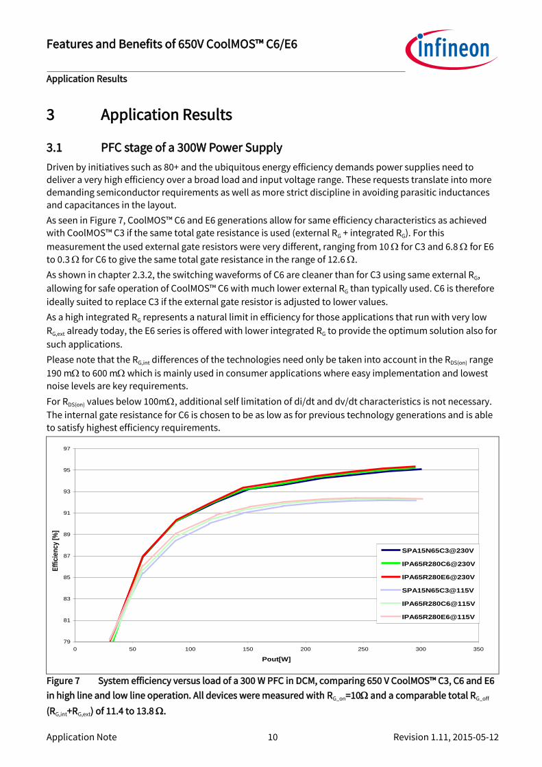
3.1 PFC stage of a 300W Power Supply
Driven by initiatives such as 80+ and the ubiquitous energy efficiency demands power supplies need to
deliver a very high efficiency over a broad load and input voltage range. These requests translate into more
demanding semiconductor requirements as well as more strict discipline in avoiding parasitic inductances and capacitances in the layout.
As seen in Figure 7, CoolMOS™ C6 and E6 generations allow for same efficiency characteristics as achieved with CoolMOS™ C3 if the same total gate resistance is used (external RG + integrated RG). For this
measurement the used external gate resistors were very different, ranging from 10 for C3 and 6.8 for E6
to 0.3 for C6 to give the same total gate resistance in the range of 12.6 .
As shown in chapter 2.3.2, the switching waveforms of C6 are cleaner than for C3 using same external RG,
allowing for safe operation of CoolMOS™ C6 with much lower external RG than typically used. C6 is therefore
ideally suited to replace C3 if the external gate resistor is adjusted to lower values.
As a high integrated RG represents a natural limit in efficiency for those applications that run with very low
RG,ext already today, the E6 series is offered with lower integrated RG to provide the optimum solution also for
such applications.
Please note that the RG,int differences of the technologies need only be taken into account in the RDS(on) range
190 m to 600 m which is mainly used in consumer applications where easy implementation and lowest
noise levels are key requirements.
For RDS(on) values below 100m, additional self limitation of di/dt and dv/dt characteristics is not necessary.
The internal gate resistance for C6 is chosen to be as low as for previous technology generations and is able
to satisfy highest efficiency requirements.
Figure 7 System efficiency versus load of a 300 W PFC in DCM, comparing 650 V CoolMOS™ C3, C6 and E6
in high line and low line operation. All devices were measured with RG_on=10 and a comparable total RG_off
(RG,int+RG,ext) of 11.4 to 13.8 .
79
81
83
85
87
89
91
93
95
97
0 50 100 150 200 250 300 350
Pout[W]
Eff
icie
ncy
[%
]
SPA15N65C3@230V
IPA65R280C6@230V
IPA65R280E6@230V
SPA15N65C3@115V
IPA65R280C6@115V
IPA65R280E6@115V

Features and Benefits of 650V CoolMOS™ C6/E6
Product Portfolio and Naming System
Application Note 11 Revision 1.11, 2015-05-12
4 Product Portfolio and Naming System 650V CoolMOS™ C6 and E6 series follow the same naming guidelines as already established with the CP
series e.g. IPP65R099C6, where I stands for Infineon Technologies, P for power MOSFETs, P for the package TO-220, 65 for the voltage class (divided by 10), R099 for the on-state resistance in milliohms and C6 for the name of the series.
Figure 8 Portfolio of 650 V CoolMOS™ C6
Figure 9 Portfolio of 650 V CoolMOS™ E6

Features and Benefits of 650V CoolMOS™ C6/E6
Product Portfolio and Naming System
Application Note 12 Revision 1.11, 2015-05-12
Revision History
Major changes since the last revision
Revision Description of change
1.0 First Release
1.1 Modify front page contents; update CoolMOS C6 and E6 portfolios in page #11

Published by
Infineon Technologies AG
81726 Munich, Germany
© 2015 Infineon Technologies AG. All Rights Reserved.
Do you have a question about any
aspect of this document?
Email: [email protected]
Document reference
Legal Disclaimer THE INFORMATION GIVEN IN THIS APPLICATION NOTE (INCLUDING BUT NOT LIMITED TO CONTENTS OF REFERENCED WEBSITES) IS GIVEN AS A HINT FOR THE IMPLEMENTATION OF THE INFINEON TECHNOLOGIES COMPONENT ONLY AND SHALL NOT BE REGARDED AS ANY DESCRIPTION OR WARRANTY OF A CERTAIN FUNCTIONALITY, CONDITION OR QUALITY OF THE INFINEON TECHNOLOGIES COMPONENT. THE RECIPIENT OF THIS APPLICATION NOTE MUST VERIFY ANY FUNCTION DESCRIBED HEREIN IN THE REAL APPLICATION. INFINEON TECHNOLOGIES HEREBY DISCLAIMS ANY AND ALL WARRANTIES AND LIABILITIES OF ANY KIND (INCLUDING WITHOUT LIMITATION WARRANTIES OF NON-INFRINGEMENT OF INTELLECTUAL PROPERTY RIGHTS OF ANY THIRD PARTY) WITH RESPECT TO ANY AND ALL INFORMATION GIVEN IN THIS APPLICATION NOTE.
Information For further information on technology, delivery terms and conditions and prices, please contact the nearest Infineon Technologies Office (www.infineon.com).
Warnings Due to technical requirements, components may contain dangerous substances. For information on the types in question, please contact the nearest Infineon Technologies Office. Infineon Technologies components may be used in life-support devices or systems only with the express written approval of Infineon Technologies, if a failure of such components can reasonably be expected to cause the failure of that life-support device or system or to affect the safety or effectiveness of that device or system. Life support devices or systems are intended to be implanted in the human body or to support and/or maintain and sustain and/or protect human life. If they fail, it is reasonable to assume that the health of the user or other persons may be endangered.
www.infineon.com
Trademarks of Infineon Technologies AG AURIX™, C166™, CanPAK™, CIPOS™, CIPURSE™, CoolGaN™, CoolMOS™, CoolSET™, CoolSiC™, CORECONTROL™, CROSSAVE™, DAVE™, DI-POL™, DrBLADE™, EasyPIM™, EconoBRIDGE™, EconoDUAL™, EconoPACK™, EconoPIM™, EiceDRIVER™, eupec™, FCOS™, HITFET™, HybridPACK™, ISOFACE™, IsoPACK™, i-Wafer™, MIPAQ™, ModSTACK™, my-d™, NovalithIC™, OmniTune™, OPTIGA™, OptiMOS™, ORIGA™, POWERCODE™, PRIMARION™, PrimePACK™, PrimeSTACK™, PROFET™, PRO-SIL™, RASIC™, REAL3™, ReverSave™, SatRIC™, SIEGET™, SIPMOS™, SmartLEWIS™, SOLID FLASH™, SPOC™, TEMPFET™, thinQ!™, TRENCHSTOP™, TriCore™.
Other Trademarks Advance Design System™ (ADS) of Agilent Technologies, AMBA™, ARM™, MULTI-ICE™, KEIL™, PRIMECELL™, REALVIEW™, THUMB™, µVision™ of ARM Limited, UK. ANSI™ of American National Standards Institute. AUTOSAR™ of AUTOSAR development partnership. Bluetooth™ of Bluetooth SIG Inc. CAT-iq™ of DECT Forum. COLOSSUS™, FirstGPS™ of Trimble Navigation Ltd. EMV™ of EMVCo, LLC (Visa Holdings Inc.). EPCOS™ of Epcos AG. FLEXGO™ of Microsoft Corporation. HYPERTERMINAL™ of Hilgraeve Incorporated. MCS™ of Intel Corp. IEC™ of Commission Electrotechnique Internationale. IrDA™ of Infrared Data Association Corporation. ISO™ of INTERNATIONAL ORGANIZATION FOR STANDARDIZATION. MATLAB™ of MathWorks, Inc. MAXIM™ of Maxim Integrated Products, Inc. MICROTEC™, NUCLEUS™ of Mentor Graphics Corporation. MIPI™ of MIPI Alliance, Inc. MIPS™ of MIPS Technologies, Inc., USA. muRata™ of MURATA MANUFACTURING CO., MICROWAVE OFFICE™ (MWO) of Applied Wave Research Inc., OmniVision™ of OmniVision Technologies, Inc. Openwave™ of Openwave Systems Inc. RED HAT™ of Red Hat, Inc. RFMD™ of RF Micro Devices, Inc. SIRIUS™ of Sirius Satellite Radio Inc. SOLARIS™ of Sun Microsystems, Inc. SPANSION™ of Spansion LLC Ltd. Symbian™ of Symbian Software Limited. TAIYO YUDEN™ of Taiyo Yuden Co. TEAKLITE™ of CEVA, Inc. TEKTRONIX™ of Tektronix Inc. TOKO™ of TOKO KABUSHIKI KAISHA TA. UNIX™ of X/Open Company Limited. VERILOG™, PALLADIUM™ of Cadence Design Systems, Inc. VLYNQ™ of Texas Instruments Incorporated. VXWORKS™, WIND RIVER™ of WIND RIVER SYSTEMS, INC. ZETEX™ of Diodes Zetex Limited. Last Trademarks Update 2014-07-17
Edition 2015-05-12
AN_201505_PL52_009