Embed Size (px)
Citation preview

Application Note AN050
Using the CC1101 in the European 868 MHz SRD band
By S. Hellan and F. Storvik Keywords • CC1101 • ETSI EN 300 220
1 Introduction
The CC1101 is a truly low-cost, highly integrated and very flexible RF transceiver. The CC1101 is primarily designed for use in low-power applications in the 315, 433, 868 and 915 MHz SRD/ISM bands.
This application note describes how to use the CC1101 in the European 863 – 870 MHz SRD frequency bands in order to comply with EN 300 220 requirements.
SWRA146A Page 1 of 25

Application Note AN050
Table of Contents KEYWORDS ................................................................................................................1 1 INTRODUCTION ..............................................................................................1 2 ABBREVIATIONS.............................................................................................4 3 FREQUENCY BANDS......................................................................................5 4 COMMENTS TO REQUIREMENTS .............................................................6
4.1 TRANSMITTER PARAMETERS.........................................................................6 4.1.1 Requirement 8.1: Frequency error or frequency drift......................................................6 4.1.2 Requirement 8.4: Spread spectrum modulation ...............................................................6 4.1.3 Requirement 8.5: Transient power ...................................................................................6 4.1.4 Requirement 8.7: Modulation bandwidth for wideband equipment .................................7 4.1.5 Requirement 8.9: Frequency stability under low voltage conditions. ..............................7 4.1.6 Requirement 8.10: Duty cycle ..........................................................................................7 4.1.7 Requirement 8.11: Principle for Listen Before Talk (LBT) ..............................................7
4.2 RECEIVER PARAMETERS ...............................................................................7 4.2.1 Requirement 9.1: Maximum useable sensitivity (conducted) ...........................................7 4.2.2 Requirement 9.2: Receiver LBT threshold and transmitter max on-time .........................8 4.2.3 Requirement 9.3: Adjacent channel selectivity.................................................................8
5 863 - 870 MHZ, FHSS WITH CHANNEL SPACING OF 100 KHZ (G).....9 5.1 TRANSMITTER PARAMETERS.........................................................................9
5.1.1 Requirement 8.2: Carrier power (conducted) ..................................................................9 5.1.2 Requirement 8.3 Effective radiated power .......................................................................9 5.1.3 Requirement 8.5: Transient power ...................................................................................9 5.1.4 Requirement 8.6: Adjacent channel power (ACP)..........................................................10 5.1.5 Requirement 8.7: Modulation bandwidth for wideband equipment ...............................11 5.1.6 Requirement 8.8: Spurious emission ..............................................................................11
5.2 RECEIVER PARAMETERS..............................................................................11 5.2.1 Requirement 9.1: Maximum useable sensitivity (conducted) .........................................11 5.2.2 Requirement 9.2: Receiver LBT threshold and transmitter max on-time .......................11 5.2.3 Requirement 9.4: Blocking or desensitization. ...............................................................11
6 868 - 868.6 MHZ, NO CHANNEL SPACING (G1).....................................13 6.1 TRANSMITTER PARAMETERS.......................................................................13
6.1.1 Requirement 8.2: Carrier power (conducted) ................................................................13 6.1.2 Requirement 8.3 Effective radiated power .....................................................................13 6.1.3 Requirement 8.5: Transient power .................................................................................13 6.1.4 Requirement 8.6: Adjacent channel power (ACP)..........................................................13 6.1.5 Requirement 8.7: Modulation bandwidth for wideband equipment ...............................13 6.1.6 Requirement 8.8: Spurious emission ..............................................................................14
6.2 RECEIVER PARAMETERS .............................................................................14 6.2.1 Requirement 9.1: Maximum useable sensitivity (conducted) .........................................14 6.2.2 Requirement 9.2: Receiver LBT threshold and transmitter max on-time .......................15 6.2.3 Requirement 9.4: Blocking or desensitization. ...............................................................15
7 868.7 - 869.2 MHZ, NO CHANNEL SPACING (G2) .................................16 7.1 TRANSMITTER PARAMETERS.......................................................................16
7.1.1 Requirement 8.2: Carrier power (conducted) ................................................................16 7.1.2 Requirement 8.3 Effective radiated power .....................................................................16 7.1.3 Requirement 8.5: Transient power .................................................................................16 7.1.4 Requirement 8.6: Adjacent channel power (ACP)..........................................................16 7.1.5 Requirement 8.7: Modulation bandwidth for wideband equipment ...............................16 7.1.6 Requirement 8.8: Spurious emission ..............................................................................17
7.2 RECEIVER PARAMETERS .............................................................................17 7.2.1 Requirement 9.1: Maximum useable sensitivity (conducted) .........................................17 7.2.2 Requirement 9.2: Receiver LBT threshold and transmitter max on-time .......................18
SWRA146A Page 2 of 25

Application Note AN050
7.2.3 Requirement 9.4: Blocking or desensitization. ...............................................................18 8 869.4 - 869.65 MHZ, NO CHANNEL SPACING (G3) ...............................19
8.1 TRANSMITTER PARAMETERS.......................................................................19 8.1.1 Requirement 8.2: Carrier power (conducted) ................................................................19 8.1.2 Requirement 8.3 Effective radiated power .....................................................................19 8.1.3 Requirement 8.5: Transient power .................................................................................19 8.1.4 Requirement 8.6: Adjacent channel power (ACP)..........................................................19 8.1.5 Requirement 8.7: Modulation bandwidth for wideband equipment ...............................19 8.1.6 Requirement 8.8: Spurious emission ..............................................................................20
8.2 RECEIVER PARAMETERS .............................................................................20 8.2.1 Requirement 9.1: Maximum useable sensitivity (conducted) .........................................20 8.2.2 Requirement 9.2: Receiver LBT threshold and transmitter max on-time .......................20 8.2.3 Requirement 9.4: Blocking or desensitization. ...............................................................21
9 869.7 - 870 MHZ, NO CHANNEL SPACING (G4).....................................22 9.1 TRANSMITTER PARAMETERS.......................................................................22
9.1.1 Requirement 8.2: Carrier power (conducted) ................................................................22 9.1.2 Requirement 8.3 Effective radiated power .....................................................................22 9.1.3 Requirement 8.5: Transient power .................................................................................22 9.1.4 Requirement 8.6: Adjacent channel power (ACP)..........................................................22 9.1.5 Requirement 8.7: Modulation bandwidth for wideband equipment ...............................22 9.1.6 Requirement 8.8: Spurious emission ..............................................................................23
9.2 RECEIVER PARAMETERS .............................................................................23 9.2.1 Requirement 9.1: Maximum useable sensitivity (conducted) .........................................23 9.2.2 Requirement 9.2: Receiver LBT threshold and transmitter max on-time .......................23 9.2.3 Requirement 9.4: Blocking or desensitization. ...............................................................24
10 REFERENCES.................................................................................................25 11 GENERAL INFORMATION..........................................................................25
11.1 DOCUMENT HISTORY...................................................................................25
SWRA146A Page 3 of 25

Application Note AN050
2 Abbreviations
ACP Adjacent Channel Power BOD Brown-Out Detection CEPT European Conference of Postal and Telecommunications
Administrations EM Evaluation module ERC European Radiocommunications Committee ETSI European Telecommunications Standards Institute GFSK Gaussian Frequency Shift Keying ISM Industrial, Scientific, Medical MBW Modulation Bandwidth MCU Microcontroller Unit OBW Occupied Bandwidth PLL Phase Locked Loop ppm Parts Per Million RBW Resolution Bandwidth SRD Short Range Device
SWRA146A Page 4 of 25
Application Note AN050
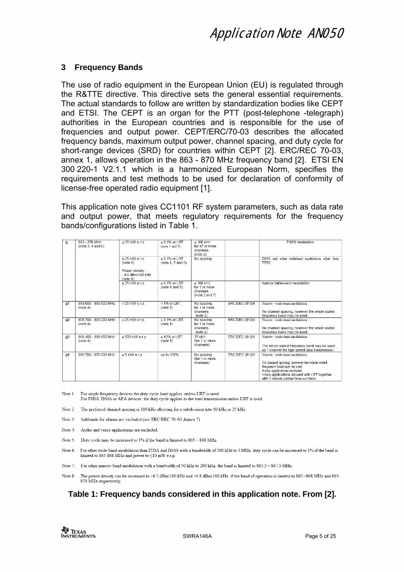
3 Frequency Bands
The use of radio equipment in the European Union (EU) is regulated through the R&TTE directive. This directive sets the general essential requirements. The actual standards to follow are written by standardization bodies like CEPT and ETSI. The CEPT is an organ for the PTT (post-telephone -telegraph) authorities in the European countries and is responsible for the use of frequencies and output power. CEPT/ERC/70-03 describes the allocated frequency bands, maximum output power, channel spacing, and duty cycle for short-range devices (SRD) for countries within CEPT [2]. ERC/REC 70-03, annex 1, allows operation in the 863 - 870 MHz frequency band [2]. ETSI EN 300 220-1 V2.1.1 which is a harmonized European Norm, specifies the requirements and test methods to be used for declaration of conformity of license-free operated radio equipment [1]. This application note gives CC1101 RF system parameters, such as data rate and output power, that meets regulatory requirements for the frequency bands/configurations listed in Table 1.
Table 1: Frequency bands considered in this application note. From [2].
SWRA146A Page 5 of 25

Application Note AN050
For details on the regulatory limits in the 863 – 870 MHz SRD frequency bands, please refer to the ETSI EN 300 220-1 V2.1.1 standard [1] and ERC Recommendation 70-03 [2]. These can be downloaded from www.etsi.org and www.ero.dk. The CC1101EM reference design [3] has been used for all measurements. The register settings used are available from the SmartRF® Studio sotware [4].
4 Comments to Requirements
EN 300 220-1 V2.1.1 specifies both tests of the RF performance and the protocol (SW). The latter is not considered in this application note.
4.1 Transmitter Parameters
4.1.1 Requirement 8.1: Frequency error or frequency drift The frequency error or drift is due to crystal inaccuracies. This requirement is therefore a test of the crystal used and not covered in this application note. Note that ETSI EN 300 220-1 extreme condition is -10°C to +55°C.
4.1.2 Requirement 8.4: Spread spectrum modulation This is a test of the protocol and not considered in this application note.
4.1.3 Requirement 8.5: Transient power Transient power is the power falling into adjacent spectrum when switching the transmitter on/off during normal operation [1]. For a channelized system the transient power shall be measured at the channel that is two channels away (alternate channel) as well as at 4 and 10 times the channel spacing of the equipment. The alternate channel and 4th and 10th channel limits are in the middle of the respective channels as opposed to channel edges. As an example, for 100 kHz channel spacing alternate channel shall be measured at ±200 kHz, 4th channel at ±400 kHz, and 10th channel at ±1 MHz offsets. For a non-channelized system EN 300 220-1 does not specify where to measure transient power. In this application note the whole sub-band is defined as the channel for a single channel system. As an example, operating at 869.5 MHz in the 869.4 – 869.65 MHz sub-band the transient power measurements are done at 869.5 MHz ±2·250 kHz, 869.5 MHz ±4·250 kHz, and 869.5 MHz ±10·250 kHz. The spectrum analyzer RBW affects the transient power measurements. EN 300 220-1 states that a spectrum analyzer can be used if the RBW is equivalent to the filter characteristics defined in annex B [1].
SWRA146A Page 6 of 25

Application Note AN050
FSQ and FSIQ7 Rhode&Schwartz spectrum analyzers were used to measure CC1101 transient power. The RBW was set to 10 kHz in the measurements. The filter response of the FSQ and FSIQ7 Rhode&Schwartz spectrum analyzers, with an RBW of 10 kHz, is a conservative choice in terms of meeting the filter characteristics defined in EN 300 220-1, annex B [1] .
4.1.4 Requirement 8.7: Modulation bandwidth for wideband equipment The 99% occupied bandwidth (OBW) shall be measured. The difference between the upper and lower frequencies where the output power envelope crosses the –36 dBm spurious limit shall be measured (MBW36). The larger of these two measurements shall be used as the modulation bandwidth. The frequency error or drift shall be included so that the total modulation bandwidth (MBWtot) is the sum of the frequency error and MBW36/OBW. The modulation bandwidth shall be measured in 300 Hz RBW. As an example, assuming a ±10 ppm initial crystal tolerance, and ±10 ppm temperature drift, the total error is 40 ppm. This corresponds to 868 MHz· 40 ppm = 35 kHz at 868 MHz operation.
4.1.5 Requirement 8.9: Frequency stability under low voltage conditions.
The operating equipment shall remain on channel while the supply voltage is decreased until it ceases to function. In the measurements the CC1101 supply voltage was set to 1.8 / 3.0 / 3.6 V and the VCO and PLL calibrated for all sub-bands. The voltage was then stepped down in 10 mV steps towards zero for all three supply voltage settings, while the spectrum was monitored. The CC1101 remained on channel down to 1.5 V in all three cases. Note that the CC1101 does not have a brown-out-detector (BOD) so the external MCU must turn off CC1101 before the supply voltage drops below 1.5 V.
4.1.6 Requirement 8.10: Duty cycle This is a test of the protocol and not considered in this application note.
4.1.7 Requirement 8.11: Principle for Listen Before Talk (LBT) This is a test of the protocol and not considered in this application note.
4.2 Receiver Parameters
4.2.1 Requirement 9.1: Maximum useable sensitivity (conducted) The limit for useable sensitivity is given by
SWRA146A Page 7 of 25
Application Note AN050
10716
log10 −=BWySensitivit [dBm]
where BW is the RX filter bandwidth in kHz.
4.2.2 Requirement 9.2: Receiver LBT threshold and transmitter max on-time
The LBT threshold is the level at which the receiver determines if the channel is available for use or not. If the input signal is above this threshold the channel is busy. Conversely, if the input signal is below this threshold the channel is available for use. Transmitter maximum on-time is not considered in this application as this is related to the protocol (SW).
4.2.3 Requirement 9.3: Adjacent channel selectivity This is a requirement for receiver class 1 only. Receiver class 1 is for devices serving systems where failure may result in a physical risk to a person [1]. CC1101 does not meet receiver class 1 adjacent channel selectivity requirements.
SWRA146A Page 8 of 25

Application Note AN050
5 863 - 870 MHz, FHSS with Channel Spacing of 100 kHz (g)
The adjacent channel power (ACP) limits the output power to +5 dBm in this frequency band (see Requirement 8.6: Adjacent channel power (ACP)). The following system parameters were used for the tests referred to in this section:
Baud rate [kBaud]
Modulation format
Frequency deviation [kHz]
Output power [dBm]
RX channel filter bandwidth [kHz]
1.2 GFSK 5.2 +5 58 38.4 GFSK 14.3 +5 101
Table 2: System parameters for tests in the 863 - 870 MHz frequency band
5.1 Transmitter Parameters
5.1.1 Requirement 8.2: Carrier power (conducted) Maximum +14 dBm output power is allowed. The CC1101 has a maximum output power of +10 dBm.
5.1.2 Requirement 8.3 Effective radiated power Maximum +14 dBm output power is allowed. The CC1101 has a maximum output power of +10 dBm.
5.1.3 Requirement 8.5: Transient power Figure 1 and Figure 2 show that the CC1101 is compliant for both 1.2 kBaud and 38.4 kBaud data rates. Alternate channel is at ±200 kHz, 4th channel at ±400 kHz, and 10th channel at ±1 MHz offsets. PA power ramp-up must be used to meet the transient power regulatory requirements, which are -27 dBm for the alternate channel and -36 dBm for the 4th and 10th channels.
SWRA146A Page 9 of 25

Application Note AN050
Transient Power 1.2 kBaud GFSK
-60,0
-50,0
-40,0
-30,0
-20,0
-10,0
0,0
10,0
1050 95
040
030
024
022
020
018
016
010
0 010
016
018
020
022
024
030
040
095
010
50
Offset [kHz]
Pow
er [d
Bm
]
PowerLimit
Figure 1: Typical transient power at +5 dBm output power, 1.2 kBaud data
rate
Transient Power 38.4 kBaud GFSK
-60,0
-50,0
-40,0
-30,0
-20,0
-10,0
0,0
10,0
1050 95
040
030
024
022
020
018
016
010
0 010
016
018
020
022
024
030
040
095
010
50
Offset [kHz]
Pow
er [d
Bm
]
PowerLimit
Figure 2: Typical transient power at +5 dBm output power, 38.4 kBaud data
rate
5.1.4 Requirement 8.6: Adjacent channel power (ACP) The limits for power in the adjacent channels are -37 dBm at normal conditions and -32 dBm at extreme conditions (-10°C to +55°C).
SWRA146A Page 10 of 25

Application Note AN050
The ACP puts an upper limit on the output power with the spectrum analyzer RBW set to 100 Hz. The CC1101 ACP, with +5 dBm output power, is typically -38 dBm for 1.2 kBaud and 38.4 kBaud data rate.
5.1.5 Requirement 8.7: Modulation bandwidth for wideband equipment This test only applies to channel spacing of >200 kHz.
5.1.6 Requirement 8.8: Spurious emission The spurious emission is below the EN 300-220-1 requirements. Note that there is one spur at 699 MHz, which is close to limit at -54 dBm.
5.2 Receiver parameters
5.2.1 Requirement 9.1: Maximum useable sensitivity (conducted)
System parameters CC1101 sensitivity [dBm]
Limit [dBm]
1.2 kBaud, GFSK, 5.2 kHz deviation, 58 kHz RX filter bandwidth
-111 -101.4
38.4 kBaud, GFSK, 14.3 kHz deviation, 101 kHz RX filter bandwidth
-103 -99
Table 3: Typical CC1101 sensitivity performance and EN 300 220 limits
5.2.2 Requirement 9.2: Receiver LBT threshold and transmitter max on-time
The LBT threshold limit is -90 dBm for a channel spacing of 100 kHz and output power less than 20 dBm [1]. Both 1.2 kBaud and 38.4 kBaud comply with this requirement. For a given AGCCTRL2.MAX_LNA_GAIN and AGCCTRL2.MAX_DVGA_GAIN register setting the absolute threshold can be adjusted ±7 dB in steps of 1 dB using CARRIER_SENSE_ABS_THR. See CC1101 data sheet for more details. As an example, using the 1.2 kBaud register settings used for optimized sensitivity the sensitivity in RX mode is -111 dBm. In LBT mode it is better to have the threshold closer to the LBT threshold limit. The LBT threshold can be set to -104 dBm using CARRIER_SENSE_ABS_THR together with the register settings optimized sensitivity.
5.2.3 Requirement 9.4: Blocking or desensitization. The wanted signal was set 3 dB above maximum useable sensitivity in requirement 9.1. The blocking performance was measured at ±2 MHz and ±10 MHz offsets. The measurement was repeated with the wanted signal
SWRA146A Page 11 of 25

Application Note AN050
increased by 13 dB to 16 dB above the useable sensitivity limit. The latter test is only applicable for receivers with LBT. System parameters
Wanted signal level [dBm]
Jammer offset [MHz]
Jammer signal level [dBm]
Limit [dBm]
±2 -38 ≥-69 1.2 kBaud, 58 kHz RX filter bandwidth. RX mode
-98.4 ±10 -30 ≥-44
±2 -26 ≥-35 1.2 kBaud, 58 kHz RX filter bandwidth. LBT mode
-85.4 ±10 -24 ≥-35
±2 -47 ≥-69 38.4 kBaud, 101 kHz RX filter bandwidth. RX mode
-98.4 ±10 -37 ≥-44
±2 -33 ≥-35 38.4 kBaud, 101 kHz RX filter bandwidth. LBT mode
-85.4 ±10 -25 ≥-35
Table 4: Typical CC1101 blocking performance and EN 300 220 limits
SWRA146A Page 12 of 25

Application Note AN050
6 868 - 868.6 MHz, No Channel Spacing (g1)
The following system parameters were used for the tests referred to in this section:
Baud rate [kBaud]
Modulation format
Frequency deviation [kHz]
Output power [dBm]
RX channel filter bandwidth [kHz]
1.2 GFSK 5.2 +10 58 38.4 GFSK 20 +10 101 76.8 GFSK 32 +10 203 100 GFSK 47 +10 270 175 GFSK 95 +10 464
Table 5: System parameters for tests in the 868 - 868.6 MHz frequency band
6.1 Transmitter Parameters
6.1.1 Requirement 8.2: Carrier power (conducted) Maximum +14 dBm output power is allowed. The CC1101 has a maximum output power of +10 dBm.
6.1.2 Requirement 8.3 Effective radiated power Maximum +14 dBm output power is allowed. The CC1101 has a maximum output power of +10 dBm.
6.1.3 Requirement 8.5: Transient power The 868 – 868.6 MHz sub-band is 600 kHz wide. The transient power measurements are performed at ±2·600 kHz, ±4·600 kHz, and ±10·600 kHz offsets. At ±1.2 MHz offset the CC1101 has more than 10 dB margin to the -27 dBm limit.
6.1.4 Requirement 8.6: Adjacent channel power (ACP) This only applies to narrowband systems with channel spacing <200 kHz.
6.1.5 Requirement 8.7: Modulation bandwidth for wideband equipment Assuming a ±10 ppm initial crystal tolerance, and ±10 ppm temperature drift, 35 kHz shall be added to the measured MBW/OBW. This number shall be <600 kHz.
SWRA146A Page 13 of 25
Application Note AN050
System parameters 99% OBW
[kHz] MBW [kHz]
MBWtot [kHz]
Limit [kHz]
1.2 kBaud, GFSK, 5.2 kHz deviation
11 16 51 <600
38.4 kBaud, GFSK, 20 kHz deviation
66 116 151 <600
76.8 kBaud, GFSK, 32 kHz deviation
114 168 203 <600
100 kBaud, GFSK, 47 kHz deviation
167 300 335 <600
175 kBaud, GFSK, 95 kHz deviation
390 525 560 <600
Table 6: Typical CC1101 modulation bandwidth and EN 300 220 limits
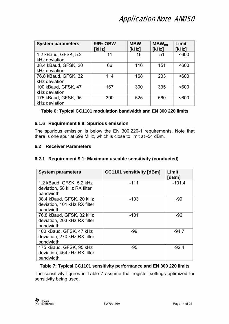
6.1.6 Requirement 8.8: Spurious emission The spurious emission is below the EN 300 220-1 requirements. Note that there is one spur at 699 MHz, which is close to limit at -54 dBm.
6.2 Receiver Parameters
6.2.1 Requirement 9.1: Maximum useable sensitivity (conducted)
System parameters CC1101 sensitivity [dBm] Limit [dBm]
1.2 kBaud, GFSK, 5.2 kHz deviation, 58 kHz RX filter bandwidth
-111 -101.4
38.4 kBaud, GFSK, 20 kHz deviation, 101 kHz RX filter bandwidth
-103 -99
76.8 kBaud, GFSK, 32 kHz deviation, 203 kHz RX filter bandwidth
-101 -96
100 kBaud, GFSK, 47 kHz deviation, 270 kHz RX filter bandwidth
-99 -94.7
175 kBaud, GFSK, 95 kHz deviation, 464 kHz RX filter bandwidth
-95 -92.4
Table 7: Typical CC1101 sensitivity performance and EN 300 220 limits The sensitivity figures in Table 7 assume that register settings optimized for sensitivity being used.
SWRA146A Page 14 of 25

Application Note AN050
6.2.2 Requirement 9.2: Receiver LBT threshold and transmitter max on-time
EN 300 220-1 has LBT threshold limits relative to channel spacing. A reasonable interpretation is that the 868 - 868.6 MHz sub-band has a “channel spacing” of 600 kHz and thus an LBT limit of -82 dBm when 1 channel is being used and the output power is less than 20 dBm [1]. For data rates >100 kBaud the register settings optimized for sensitivity cannot be used when doing listen before talk. The reason is that the LBT blocking requirements are then violated (covered in section 6.2.3). For data rates ≤100 kBaud the LBT threshold can be set to a higher level than the sensitivity in Table 7 by programming CARRIER_SENSE_ABS_THR and still meet the LBT blocking requirements.
6.2.3 Requirement 9.4: Blocking or desensitization. For receivers with LBT operating at data rates >100 kBaud it is recommended to use a higher MAX_LNA_GAIN register setting in LBT mode compared to RX mode to meet the -35 dBm limit at ±2 MHz and ±10 MHz offsets with the wanted signal 16 dB above the useable sensitivity limit. A higher MAX_LNA_GAIN register setting corresponds to a lower maximum LNA gain and hence lower sensitivity but better blocking performance. In normal RX mode, the CC1101 meets the blocking performance at ±2 MHz and ±10 MHz offsets (-69 dBm and -44 dBm respectively) using the register settings optimized for sensitivity for all data rates.
SWRA146A Page 15 of 25

Application Note AN050
7 868.7 - 869.2 MHz, No Channel Spacing (g2)
The following system parameters were used for the tests referred to in this section:
Baud rate [kBaud]
Modulation format
Frequency deviation [kHz]
Output power [dBm]
RX channel filter bandwidth [kHz]
1.2 GFSK 5.2 +10 58 38.4 GFSK 20 +10 101 76.8 GFSK 32 +10 203 100 GFSK 47 +10 270
Table 8: System parameters for tests in the 868.7 - 869.2 MHz frequency band
7.1 Transmitter Parameters
7.1.1 Requirement 8.2: Carrier power (conducted) Maximum +14 dBm output power is allowed. The CC1101 has a maximum output power of +10 dBm.
7.1.2 Requirement 8.3 Effective radiated power Maximum +14 dBm output power is allowed. The CC1101 has a maximum output power of +10 dBm.
7.1.3 Requirement 8.5: Transient power The 868.7 – 869.2 MHz sub-band is 500 kHz wide. The transient power measurements are performed at ±2·500 kHz, ±4·500 kHz, and ±10·500 kHz offsets. At ±1.0 MHz offset the CC1101 has approximately 15 dB margin to the -27 dBm limit.
7.1.4 Requirement 8.6: Adjacent channel power (ACP) This only applies to narrowband systems with channel spacing <200 kHz.
7.1.5 Requirement 8.7: Modulation bandwidth for wideband equipment By assuming a ±10 ppm initial crystal variation, and ±10 ppm temperature drift, 35 kHz shall be added to the measured MBW/OBW. This number shall be <500 kHz.
SWRA146A Page 16 of 25

Application Note AN050
System parameters 99% OBW [kHz]
MBW [kHz]
MBWtot [kHz]
Limit [kHz]
1.2 kBaud, GFSK, 5.2 kHz deviation
11 16 51 <500
38.4 kBaud, GFSK, 20 kHz deviation
66 116 151 <500
76.8 kBaud, GFSK, 32 kHz deviation
114 168 203 <500
100 kBaud, GFSK, 47 kHz deviation
167 300 335 <500
Table 9: Typical CC1101 modulation bandwidth and EN 300 220 limits
7.1.6 Requirement 8.8: Spurious emission The spurious emission is below the EN 300-220 requirements. Note that there is one spur at 699 MHz, which is close to limit at -54 dBm.
7.2 Receiver Parameters
7.2.1 Requirement 9.1: Maximum useable sensitivity (conducted)
System parameters CC1101 sensitivity [dBm]
Limit [dBm]
1.2 kBaud, GFSK, 5.2 kHz deviation, 58 kHz RX filter bandwidth
-111 -101.4
38.4 kBaud, GFSK, 20 kHz deviation, 101 kHz RX filter bandwidth
-103 -99
76.8 kBaud, GFSK, 32 kHz deviation, 203 kHz RX filter bandwidth
-101 -96
100 kBaud, GFSK, 47 kHz deviation, 270 kHz RX filter bandwidth
-99 -94.7
Table 10: Typical CC1101 sensitivity performance and EN 300 220 limits
SWRA146A Page 17 of 25

Application Note AN050
7.2.2 Requirement 9.2: Receiver LBT threshold and transmitter max on-time
EN 300 220-1 has LBT threshold limits relative to channel spacing. A reasonable interpretation is that the 868.7 - 869.2 MHz sub-band has a “channel spacing” of 500 kHz and thus an LBT limit of -83 dBm when 1 channel is being used and the output power is less than 20 dBm [1]. For data rates ≤100 kBaud the LBT threshold can be set to a higher level than the sensitivity in Table 10 by programming CARRIER_SENSE_ABS_THR and still meet the LBT blocking requirements.
7.2.3 Requirement 9.4: Blocking or desensitization. For receivers with LBT the blocking requirements are met using the register settings optimized for sensitivity for all data rates in Table 10. In normal RX mode the blocking requirements are met using the register settings optimized for sensitivity for all data rates in Table 10.
SWRA146A Page 18 of 25

Application Note AN050
8 869.4 - 869.65 MHz, No Channel Spacing (g3)
A 27 MHz crystal frequency is recommended used when operating in this frequency band for maximum CC1101 output power. The following system parameters were used for the tests referred to in this section:
Baud rate [kBaud]
Modulation format
Frequency deviation [kHz]
Output power [dBm]
RX channel filter bandwidth [kHz]
1.2 GFSK 5.2 +10 58 38.4 GFSK 20 +10 101 76.8 GFSK 32 +10 203
Table 11: System parameters for tests in the 869.4 - 869.65 frequency band
8.1 Transmitter Parameters
8.1.1 Requirement 8.2: Carrier power (conducted) Maximum +27 dBm output power is allowed. The CC1101 has a maximum output power of +10 dBm.
8.1.2 Requirement 8.3 Effective radiated power Maximum +27 dBm output power is allowed. The CC1101 has a maximum output power of +10 dBm.
8.1.3 Requirement 8.5: Transient power The 869.4 – 869.65 MHz sub-band is 250 kHz wide. The transient power measurements are performed at ±2·250 kHz, ±4·250 kHz, and ±10·250 kHz offsets. At ±500 kHz offset the CC1101 has approximately 7 dB margin to the -27 dBm limit. At ±1 MHz offset the CC1101 has approximately 7 dB margin to the -36 dBm limit.
8.1.4 Requirement 8.6: Adjacent channel power (ACP) This only applies to narrowband systems with channel spacing <200 kHz.
8.1.5 Requirement 8.7: Modulation bandwidth for wideband equipment By assuming a ±10 ppm initial crystal variation, and ±10 ppm temperature drift, 35 kHz shall be added to the measured MBW/OBW. This number shall be <250 kHz.
SWRA146A Page 19 of 25

Application Note AN050
System parameters 99% OBW [kHz]
MBW [kHz]
MBWtot [kHz]
Limit [kHz]
1.2 kBaud, GFSK, 5.2 kHz deviation
11 16 51 <250
38.4 kBaud, GFSK, 20 kHz deviation
66 116 151 <250
76.8 kBaud, GFSK, 32 kHz deviation
114 168 203 <250
Table 12: Typical CC1101 modulation bandwidth and EN 300 220 limits
8.1.6 Requirement 8.8: Spurious emission Close-in spurs increases in power as the frequency increases towards 870 MHz when using a 26 MHz crystal. The maximum output power is then limited to +7 dBm. With a 27 MHz crystal the maximumCC1101 output power of +10 dBm can be used.
8.2 Receiver Parameters
8.2.1 Requirement 9.1: Maximum useable sensitivity (conducted)
System parameters CC1101 sensitivity [dBm]
Limit [dBm]
1.2 kBaud, GFSK, 5.2 kHz deviation, 58 kHz RX filter bandwidth
-111 -101.4
38.4 kBaud, GFSK, 20 kHz deviation, 101 kHz RX filter bandwidth
-103 -99
76.8 kBaud, GFSK, 32 kHz deviation, 203 kHz RX filter bandwidth
-101 -96
Table 13: Typical CC1101 sensitivity performance and EN 300 220 limits
8.2.2 Requirement 9.2: Receiver LBT threshold and transmitter max on-time
EN 300 220-1 has LBT threshold limits relative to channel spacing. A reasonable interpretation is that the 869.4 - 869.65 MHz sub-band has a “channel spacing” of 250 kHz and thus an LBT limit of approximately -86 dBm when 1 channel is being used and the output power is less than 20 dBm [1].
SWRA146A Page 20 of 25

Application Note AN050
The data rates in Table 13 comply with this requirement. For a given AGCCTRL2.MAX_LNA_GAIN and AGCCTRL2.MAX_DVGA_GAIN register setting the absolute threshold can be adjusted ±7 dB in steps of 1 dB using CARRIER_SENSE_ABS_THR. See CC1101 data sheet for more details.
8.2.3 Requirement 9.4: Blocking or desensitization. For receivers with LBT the blocking requirements are met using the register settings optimized for sensitivity for all data rates in Table 13. In normal RX mode the blocking requirements are met using the register settings optimized for sensitivity for all data rates in Table 13.
SWRA146A Page 21 of 25

Application Note AN050
9 869.7 - 870 MHz, No Channel Spacing (g4)
A 27 MHz crystal frequency is recommended used when operating in this frequency band for maximum CC1101 output power. The following system parameters were used for the tests referred to in this section:
Baud rate [kBaud]
Modulation format
Frequency deviation [kHz]
Output power [dBm]
RX channel filter bandwidth [kHz]
1.2 GFSK 5.2 +10 58 38.4 GFSK 20 +10 101 76.8 GFSK 32 +10 203
Table 14: System parameters for tests in the 869.7 - 870 MHz frequency band
9.1 Transmitter Parameters
9.1.1 Requirement 8.2: Carrier power (conducted) Maximum +7 dBm output power is allowed. The CC1101 has a maximum output power of +10 dBm.
9.1.2 Requirement 8.3 Effective radiated power Maximum +7 dBm output power is allowed. The CC1101 has a maximum output power of +10 dBm.
9.1.3 Requirement 8.5: Transient power The 869.7 – 870 MHz sub-band is 300 kHz wide. The transient power measurements are performed at ±2·300 kHz, ±4·300 kHz, and ±10·300 kHz offsets. At ±600 kHz offset the CC1101 has approximately 10 dB margin to the -27 dBm limit. At ±1.2 MHz offset the CC1101 has approximately 4 dB margin to the -36 dBm limit.
9.1.4 Requirement 8.6: Adjacent channel power (ACP) This only applies to narrowband systems with channel spacing <200 kHz.
9.1.5 Requirement 8.7: Modulation bandwidth for wideband equipment By assuming a ±10 ppm initial crystal variation, and ±10 ppm temperature drift, 35 kHz shall be added to the measured MBW/OBW. This number shall be <300 kHz.
SWRA146A Page 22 of 25

Application Note AN050
System parameters 99% OBW [kHz]
MBW [kHz]
MBWtot [kHz]
Limit [kHz]
1.2 kBaud, GFSK, 5.2 kHz deviation
11 16 51 <300
38.4 kBaud, GFSK, 20 kHz deviation
66 116 151 <300
76.8 kBaud, GFSK, 32 kHz deviation
114 168 203 <300
Table 15: Typical CC1101 modulation bandwidth and EN 300 220 limits (measured with +10 dBm output power)
9.1.6 Requirement 8.8: Spurious emission Close-in spurs increases in power as the frequency increases towards 870 MHz when using a 26 MHz crystal. The maximum output power is then limited to +5 dBm. With a 27 MHz crystal the maximum output power of +7 dBm can be used.
9.2 Receiver Parameters
9.2.1 Requirement 9.1: Maximum useable sensitivity (conducted)
System parameters CC1101 sensitivity [dBm]
Limit [dBm]
1.2 kBaud, GFSK, 5.2 kHz deviation, 58 kHz RX filter bandwidth
-111 -101.4
38.4 kBaud, GFSK, 20 kHz deviation, 101 kHz RX filter bandwidth
-103 -99
76.8 kBaud, GFSK, 32 kHz deviation, 203 kHz RX filter bandwidth
-101 -96
Table 16: Typical CC1101 sensitivity performance and EN 300 220 limits
9.2.2 Requirement 9.2: Receiver LBT threshold and transmitter max on-time
EN 300 220-1 has LBT threshold limits relative to channel spacing. A reasonable interpretation is that the 869.7 - 870 MHz sub-band has a “channel spacing” of 300 kHz and thus an LBT limit of approximately -84.5 dBm when 1 channel is being used and the output power is less than 20 dBm [1].
SWRA146A Page 23 of 25

Application Note AN050
The data rates in Table 16 comply with this requirement. For a given AGCCTRL2.MAX_LNA_GAIN and AGCCTRL2.MAX_DVGA_GAIN register setting the absolute threshold can be adjusted ±7 dB in steps of 1 dB using CARRIER_SENSE_ABS_THR. See CC1101 data sheet for more details.
9.2.3 Requirement 9.4: Blocking or desensitization. For receivers with LBT the blocking requirements are met using the register settings optimized for sensitivity for all data rates in Table 16. In normal RX mode the blocking requirements are met using the register settings optimized for sensitivity for all data rates in Table 16.
SWRA146A Page 24 of 25
Application Note AN050
10 References
[1] ETSI EN 300 220 V2.1.1: Electromagnetic compatibility and Radio spectrum Matters (ERM); Short Range Devices (SRD); Radio equipment to be used in the 25 MHz to 1000 MHz frequency range with power levels ranging up to 500 mW”
[2] CEPT/ERC/Recommendation 70-03: “Relating to the use of Short Range Devices (SRD)”
[3] CC1101EM 868 – 915 MHz Reference Design 2.0 (swrr044.zip)
[4] SmartRF® Studio (swrc046.zip)
11 General Information
11.1 Document History Revision Date Description/Changes SWRA146A 2007.10.25 Changed the maximum recommended data rate for sub band g1,
g2, g3 and g4. SWRA146 2007.06.28 Initial release.
SWRA146A Page 25 of 25

IMPORTANT NOTICE
Texas Instruments Incorporated and its subsidiaries (TI) reserve the right to make corrections, modifications, enhancements,improvements, and other changes to its products and services at any time and to discontinue any product or service without notice.Customers should obtain the latest relevant information before placing orders and should verify that such information is current andcomplete. All products are sold subject to TI’s terms and conditions of sale supplied at the time of order acknowledgment.
TI warrants performance of its hardware products to the specifications applicable at the time of sale in accordance with TI’sstandard warranty. Testing and other quality control techniques are used to the extent TI deems necessary to support thiswarranty. Except where mandated by government requirements, testing of all parameters of each product is not necessarilyperformed.
TI assumes no liability for applications assistance or customer product design. Customers are responsible for their products andapplications using TI components. To minimize the risks associated with customer products and applications, customers shouldprovide adequate design and operating safeguards.
TI does not warrant or represent that any license, either express or implied, is granted under any TI patent right, copyright, maskwork right, or other TI intellectual property right relating to any combination, machine, or process in which TI products or servicesare used. Information published by TI regarding third-party products or services does not constitute a license from TI to use suchproducts or services or a warranty or endorsement thereof. Use of such information may require a license from a third party underthe patents or other intellectual property of the third party, or a license from TI under the patents or other intellectual property of TI.
Reproduction of TI information in TI data books or data sheets is permissible only if reproduction is without alteration and isaccompanied by all associated warranties, conditions, limitations, and notices. Reproduction of this information with alteration is anunfair and deceptive business practice. TI is not responsible or liable for such altered documentation. Information of third partiesmay be subject to additional restrictions.
Resale of TI products or services with statements different from or beyond the parameters stated by TI for that product or servicevoids all express and any implied warranties for the associated TI product or service and is an unfair and deceptive businesspractice. TI is not responsible or liable for any such statements.
TI products are not authorized for use in safety-critical applications (such as life support) where a failure of the TI product wouldreasonably be expected to cause severe personal injury or death, unless officers of the parties have executed an agreementspecifically governing such use. Buyers represent that they have all necessary expertise in the safety and regulatory ramificationsof their applications, and acknowledge and agree that they are solely responsible for all legal, regulatory and safety-relatedrequirements concerning their products and any use of TI products in such safety-critical applications, notwithstanding anyapplications-related information or support that may be provided by TI. Further, Buyers must fully indemnify TI and itsrepresentatives against any damages arising out of the use of TI products in such safety-critical applications.
TI products are neither designed nor intended for use in military/aerospace applications or environments unless the TI products arespecifically designated by TI as military-grade or "enhanced plastic." Only products designated by TI as military-grade meet militaryspecifications. Buyers acknowledge and agree that any such use of TI products which TI has not designated as military-grade issolely at the Buyer's risk, and that they are solely responsible for compliance with all legal and regulatory requirements inconnection with such use.
TI products are neither designed nor intended for use in automotive applications or environments unless the specific TI productsare designated by TI as compliant with ISO/TS 16949 requirements. Buyers acknowledge and agree that, if they use anynon-designated products in automotive applications, TI will not be responsible for any failure to meet such requirements.
Following are URLs where you can obtain information on other Texas Instruments products and application solutions:
Products Applications
Amplifiers amplifier.ti.com Audio www.ti.com/audio
Data Converters dataconverter.ti.com Automotive www.ti.com/automotive
DSP dsp.ti.com Broadband www.ti.com/broadband
Interface interface.ti.com Digital Control www.ti.com/digitalcontrol
Logic logic.ti.com Military www.ti.com/military
Power Mgmt power.ti.com Optical Networking www.ti.com/opticalnetwork
Microcontrollers microcontroller.ti.com Security www.ti.com/security
RFID www.ti-rfid.com Telephony www.ti.com/telephony
Low Power www.ti.com/lpw Video & Imaging www.ti.com/videoWireless
Wireless www.ti.com/wireless
Mailing Address: Texas Instruments, Post Office Box 655303, Dallas, Texas 75265Copyright © 2007, Texas Instruments Incorporated


![IB BDI-D112010-S01€¦ · We]tWejt Ireland UnjtedKj Flexider Milwaukee Machine Works, Inc. Spain Colùmbias,Gea HELLAN](https://img.pdfslide.net/doc/110x75/5e96a7a3879b7b5c14735c51/ib-bdi-d112010-wetwejt-ireland-unjtedkj-flexider-milwaukee-machine-works-inc.jpg)