Embed Size (px)
Citation preview

'05-8
Car Audio, Automotive LANData Communication Equipment

Contents
..........................................................................................................................................................................................................................................................................................................1 to 21 to 2......................................................................................................................................................................3 to 4......................................................................................................................................................................3 to 4
....................................................................................................................................................................................5....................................................................................................................................................................................5.................................................................................................................................................................................6.................................................................................................................................................................................6
................................................................................................................................................................................................................................................7 to 87 to 8.......................................................................................................................................................................9.......................................................................................................................................................................9...................................................................................................................................................................10...................................................................................................................................................................10
..............................................................................................................................................................................................................................11 to 1211 to 12................................................................................................................................................................13................................................................................................................................................................13
.......................................................................................................................................................14.......................................................................................................................................................14........................................................................................................................................................................................15 to 1615 to 16
.............................................................................17.............................................................................17..............................................................................................................................18..............................................................................................................................18
..................................................................................................................................................................19..................................................................................................................................................................19.........................................................................................................................20.........................................................................................................................20
.......................................................................................................................................21.......................................................................................................................................21.............................................................................................................................................................22.............................................................................................................................................................22
......................................................................................................................................................23 to 26......................................................................................................................................................23 to 26......................................................................................................27 to 30......................................................................................................27 to 30................................................................................................................31................................................................................................................31
...............................................................................................................................32...............................................................................................................................32.................................................................................................33 to 34.................................................................................................33 to 34
......................................................................................................................................................35 to 3635 to 36......................................................................................................................................................37......................................................................................................................................................37
.........................................................................................38.........................................................................................38........................................................................39........................................................................39
..............................................................................................40..............................................................................................40......................................................................................................................................................41 to 4241 to 42
.................................................................................................................43.................................................................................................................43.......................................................................44 to 46.......................................................................44 to 46
......................................................................................................................................................47 to 48......................................................................................................................................................47 to 48..............................................................................................................................................................................49 to 5049 to 50
......................................................................................................51......................................................................................................51.......................................................................................................................52 to 54.......................................................................................................................52 to 54
......................................................................................................................................................................55 to 5655 to 56........................................................................................................57........................................................................................................57........................................................................................................58........................................................................................................58
..............59..............59......................................60......................................60
..........................................................................................................................................................................61 to 6261 to 62............................................................................63 to 64............................................................................63 to 64
..........................................................65 to 66..........................................................65 to 66........................................................................................................................................................................................................................................................................67 to 6867 to 68
.......................................................................................... 69.......................................................................................... 69.................................................................................................................70.................................................................................................................70
....................................................................................................................................................71....................................................................................................................................................71...........................................................................................................72...........................................................................................................72
............................................................................................................................................................................................................................................................................73 to 7873 to 78
Combining vivid images and realistic sound Combining vivid images and realistic sound SANYO Car AudioSANYO Car Audioandand
Automotive LAN DevicesAutomotive LAN Devices
SANYO Car Audioand
Automotive LAN Devices
Automotive electronics is a field where advances Automotive electronics is a field where advances are occurring on a daily basis, notably with regard are occurring on a daily basis, notably with regard to the sound and information space realized through to the sound and information space realized through refined proprietary technologies. refined proprietary technologies. Automotive network technology controls many different Automotive network technology controls many different types of information such as automotive AV. types of information such as automotive AV. SANYO's LSIs powerfully support activities such as SANYO's LSIs powerfully support activities such as listening, watching, searching, and relaxing in this listening, watching, searching, and relaxing in this ubiquitous age, and support diverse needs with a ubiquitous age, and support diverse needs with a diversified product lineup and a broad array of diversified product lineup and a broad array of technologies. technologies. The proprietary technologies of SANYO, a world leader The proprietary technologies of SANYO, a world leader in this field, are defining the present and near future of in this field, are defining the present and near future of automotive devices.automotive devices.
Automotive electronics is a field where advances are occurring on a daily basis, notably with regard to the sound and information space realized through refined proprietary technologies. Automotive network technology controls many different types of information such as automotive AV. SANYO's LSIs powerfully support activities such as listening, watching, searching, and relaxing in this ubiquitous age, and support diverse needs with a diversified product lineup and a broad array of technologies. The proprietary technologies of SANYO, a world leader in this field, are defining the present and near future of automotive devices.
Combining vivid images and realistic sound
Automotive LANAutomotive LAN CARNET CARNET CAN CAN MOST MOSTDigital Radio System ChipsetsDigital Radio System Chipsets 1-chip Tuner 1-chip Tuner Tuner/IF-DSP Tuner/IF-DSPCar Audio DSP System ChipsetsCar Audio DSP System Chipsets Car Audio DSP Car Audio DSP Dolby Headphone IC Dolby Headphone ICCar Audio CD/MP3/WMA System ChipsetsCar Audio CD/MP3/WMA System Chipsets Super System-on-Chip Digital Servo IC with On-Chip RF System Super System-on-Chip Digital Servo IC with On-Chip RF System Compact Disc Player MP3 Decoder Compact Disc Player MP3 Decoder WMA Decoder WMA Decoder 7.5 Mbps Automotive LAN Transceiver 7.5 Mbps Automotive LAN Transceiver POF 50Mbps Automotive LAN POF 50Mbps Automotive LAN CAN Transceiver CAN Transceiver Microcontrollers Microcontrollers Four-Channel Driver IC for CD Player/Decks Four-Channel Driver IC for CD Player/Decks Five-Channel Driver IC for CD Player/Decks Five-Channel Driver IC for CD Player/Decks DVD-ROM Spindle Motor Driver IC DVD-ROM Spindle Motor Driver IC System Motor Driver IC for CD and MD Players System Motor Driver IC for CD and MD PlayersCar Audio Built-in PLL Tuner System Chipsets (1)Car Audio Built-in PLL Tuner System Chipsets (1) Bus Control Tuner IC Bus Control Tuner IC Clear Surround Control IC Includes Plus Sound Algorithm Clear Surround Control IC Includes Plus Sound Algorithm Car Audio Electronic Volume Control IC with BBE Sound Processor Car Audio Electronic Volume Control IC with BBE Sound Processor Four Channel High-Output Line Amplifier for Car Audio Four Channel High-Output Line Amplifier for Car AudioCar Audio Built-in PLL Tuner System Chipsets (2)Car Audio Built-in PLL Tuner System Chipsets (2) Car Audio Tuner IC with Built-in PLL Circuit Car Audio Tuner IC with Built-in PLL Circuit Electronic Volume and Tone Control IC for Car Audio Systems Electronic Volume and Tone Control IC for Car Audio Systems Power Amplifier Power AmplifierCar Audio Standard Tuner System ChipsetsCar Audio Standard Tuner System Chipsets System-on-Chip Tuner IC for Car Stereo Systems System-on-Chip Tuner IC for Car Stereo Systems Electronic Tuning ETR Controllers Electronic Tuning ETR ControllersMultiplexed Stereo Decoder System ChipsetsMultiplexed Stereo Decoder System Chipsets Car Stereo 17 W Two-Channel BTL AF Amplifier Car Stereo 17 W Two-Channel BTL AF Amplifier Car Stereo 20 W Two-Channel BTL AF Amplifier Car Stereo 20 W Two-Channel BTL AF Amplifier Car Radio/Car Stereo 5 W Two-Channel Power Amplifier that Requires Minimal External Components Car Radio/Car Stereo 5 W Two-Channel Power Amplifier that Requires Minimal External Components Car Radio/Car Stereo 5 W Power Amplifier that Requires Minimal External Components Car Radio/Car Stereo 5 W Power Amplifier that Requires Minimal External ComponentsFM Multiplex Broadcasting System ChipsetsFM Multiplex Broadcasting System Chipsets Mobile FM Multiplex Broadcast (DARC System) Receiver IC Mobile FM Multiplex Broadcast (DARC System) Receiver IC Mobile FM Multiplex Broadcast Receiver IC with Built-in VICS Decoder Mobile FM Multiplex Broadcast Receiver IC with Built-in VICS DecoderRDS System ChipsetsRDS System Chipsets Car Audio Electronic Tuning PLL Frequency Synthesizer Car Audio Electronic Tuning PLL Frequency Synthesizer RDS Signal-Processing System-on-Chip IC RDS Signal-Processing System-on-Chip IC RDS Demodulator ICs RDS Demodulator ICs Single-Chip RDS Signal Processing System IC Single-Chip RDS Signal Processing System ICPackage DimensionsPackage Dimensions
.....................................................................................................................................................1 to 2......................................................................................................................................................................3 to 4
....................................................................................................................................................................................5.................................................................................................................................................................................6
........................................................................................................................7 to 8.......................................................................................................................................................................9...................................................................................................................................................................10
...............................................................................................................11 to 12................................................................................................................................................................13
.......................................................................................................................................................14............................................................................................15 to 16
.............................................................................17..............................................................................................................................18
..................................................................................................................................................................19.........................................................................................................................20
.......................................................................................................................................21.............................................................................................................................................................22
......................................................................................................................................................23 to 26......................................................................................................27 to 30................................................................................................................31
...............................................................................................................................32.................................................................................................33 to 34
...........................................................................35 to 36......................................................................................................................................................37
.........................................................................................38........................................................................39
..............................................................................................40...........................................................................41 to 42
.................................................................................................................43.......................................................................44 to 46
......................................................................................................................................................47 to 48.......................................................................................49 to 50
......................................................................................................51.......................................................................................................................52 to 54
...................................................................................55 to 56........................................................................................................57........................................................................................................58
..............59......................................60
.....................................................................................61 to 62............................................................................63 to 64
..........................................................65 to 66....................................................................................................................................67 to 68
.......................................................................................... 69.................................................................................................................70
....................................................................................................................................................71...........................................................................................................72
......................................................................................................................................73 to 78
Automotive LAN CARNET CAN MOSTDigital Radio System Chipsets 1-chip Tuner Tuner/IF-DSPCar Audio DSP System Chipsets Car Audio DSP Dolby Headphone ICCar Audio CD/MP3/WMA System Chipsets Super System-on-Chip Digital Servo IC with On-Chip RF System Compact Disc Player MP3 Decoder WMA Decoder 7.5 Mbps Automotive LAN Transceiver POF 50Mbps Automotive LAN CAN Transceiver Microcontrollers Four-Channel Driver IC for CD Player/Decks Five-Channel Driver IC for CD Player/Decks DVD-ROM Spindle Motor Driver IC System Motor Driver IC for CD and MD PlayersCar Audio Built-in PLL Tuner System Chipsets (1) Bus Control Tuner IC Clear Surround Control IC Includes Plus Sound Algorithm Car Audio Electronic Volume Control IC with BBE Sound Processor Four Channel High-Output Line Amplifier for Car AudioCar Audio Built-in PLL Tuner System Chipsets (2) Car Audio Tuner IC with Built-in PLL Circuit Electronic Volume and Tone Control IC for Car Audio Systems Power AmplifierCar Audio Standard Tuner System Chipsets System-on-Chip Tuner IC for Car Stereo Systems Electronic Tuning ETR ControllersMultiplexed Stereo Decoder System Chipsets Car Stereo 17 W Two-Channel BTL AF Amplifier Car Stereo 20 W Two-Channel BTL AF Amplifier Car Radio/Car Stereo 5 W Two-Channel Power Amplifier that Requires Minimal External Components Car Radio/Car Stereo 5 W Power Amplifier that Requires Minimal External ComponentsFM Multiplex Broadcasting System Chipsets Mobile FM Multiplex Broadcast (DARC System) Receiver IC Mobile FM Multiplex Broadcast Receiver IC with Built-in VICS DecoderRDS System Chipsets Car Audio Electronic Tuning PLL Frequency Synthesizer RDS Signal-Processing System-on-Chip IC RDS Demodulator ICs Single-Chip RDS Signal Processing System ICPackage Dimensions

CARNET is a LAN that uses the ARCNET token passing bus method. CARNET is a LAN that uses the ARCNET token passing bus method.
It can achieve a high transmission speed of 7.5 Mbps. It can achieve a high transmission speed of 7.5 Mbps.
Since noise can be minimized by installing Since noise can be minimized by installing
this LAN in vehicles, such installation has this LAN in vehicles, such installation has
very little impact on other devices.very little impact on other devices.
A 7.5 Mbps automotive LAN can be configured by combining the LA2330W with a protocol IC for CARNET (ARCNET controller TMC20040C Series). On-chip driver/receiver for The audio equipment control bus On-chip driver/receiver for CAN Includes 8 non-inverted type open-collector output comparator circuits
The audio equipment control bus block, CAN block bus output withstand voltage of 18 V Vehicle signal detection block input withstand voltage of 18 V Each block is independent (incl. power supply and GND line), and each is provided with a standby function.
CARNET is a LAN that uses the ARCNET token passing bus method.
It can achieve a high transmission speed of 7.5 Mbps.
Since noise can be minimized by installing
this LAN in vehicles, such installation has
very little impact on other devices.
Features
Transceiver block for CARNET (1) Transmitter (D/A converter (3-bit), LPF (for EMI prevention), output driver) (2) Receiver (attenuator, receiving amplifier, noise elimination LPF (for reception signal), comparator (for waveform shaping) Driver/receiver block for The audio equipment control bus (1) Transmitter (output driver) (2) Receiver (receiving amplifier, hysteresis comparator (for waveform shaping) Driver/receiver block for CAN (1) Transmitter (LPF (for EMI prevention), output driver) (2) Receiver (attenuator, comparator) Non-inverted type open-collector output comparator
Functions
1-chip IC incorporating an The audio equipment control bus transceiver and comparator
The audio equipment control bus output withstand voltage of 18 V Vehicle signal detection block input withstand voltage of 18V
Features
Driver/receiver block for The audio equipment control bus (1) Transmitter (output driver) (2) Receiver (receiving amplifier, hysteresis comparator (for waveform shaping)) Non-inverted type open collector output comparator
Functions
The LA2351M is a low-noise transceiver IC for automotive LANs.
Support of either 3-bit digital or staircase signals as input signal If a 3-bit digital signal cannot be routed as an EMI countermeasure, place an R-2R ladder in the vicinity of the protocol chip and route the signal following D/A conversion, connecting it to the LPF input. A 5-Mbps or 7.5 Mbps automotive LAN can be constructed by combining the LA2351M with a protocol IC for automotive LAN (ARCNET controller TMC20040C Series). On-chip adjustment LPF Low-noise data communication is possible.
Features
Transmitter (transmit) block 1) D/A converter (3-bit) 2) LPF (for EMI prevention) 3) Output driver Receiver (receive) block 1) Receiving amplifier 2) Noise elimination LPF (for reception signal) 3) Comparator (for waveform shaping)
Functions
CARNET Automotive LAN
Hub function supporting connection of up to 8 nodes Construction of LAN with high transmission speed of 7.5 Mbps yet ultra low noise possible Twisted pair cables can be used Easy to use due to compact size
Features
3 Car Audio 4 Car Audio
TEL GPS
Radio
CD, VICS
LA2330W CARNET/transceiver Under development
LA2333T The audio equipment control bus transceiver + comparator Under development
LA2351M Transceiver for CARNET
Car navigationsystem

LA2360M Transceiver for CAN Under development
LA2361JM/LA2361AM Transceiver for CAN Under development
Under developmentLA2340M/LV2341M MOST transceiver
Sheet
Sheet
Panel
Poweredwindow
Door mirror
Door
Door
Wipers Air
conditioner
TVDVD
Speaker
Speaker
Speaker
Speaker
CAN is a high-reliability LAN for controlling body transmission devices. CAN is a high-reliability LAN for controlling body transmission devices.
CAN can achieve a high transmission rate of CAN can achieve a high transmission rate of
1 Mbps and is strong against external noise, 1 Mbps and is strong against external noise,
thus allowing stable communication.thus allowing stable communication.
The LA2360M is a transceiver IC for CAN.
ISO11898 compliant Transmission speed of 1 Mbps
CAN is a high-reliability LAN for controlling body transmission devices.
CAN can achieve a high transmission rate of
1 Mbps and is strong against external noise,
thus allowing stable communication.
Features
Transmitter (transmit) block • Output driver
Receiver (receive) block • Attenuator • Comparator
Functions
ISO11898 compliant Low power consumption
Transmission speed of 1 Mbps Low output noise
Features
Transmitter (transmit) block • Output driver
Receiver (receive) block • Attenuator • Comparator
Functions
The LA2340M is an I/V converter that can be used to configure an optical electric converter (OEC) when combined with a photo diode (PD). The LV2341M is a LED driver that can be used to configure an electric optical converter (EOC) when combined with a LED.
50-Mbps automotive LAN can be constructed with POF Standby function Transmission speed of up to 50 Mbps POF cable Power supply voltage: +5 V
Features
CAN
ISO11898 compliant
Low power consumption
Transmission speed of up to 1 Mbps
On-chip lamp signal control
MOST is an automotive LAN that uses POF (plastic optical fiber).
It allows the construction of a low-noise high-speed (50 Mbps) LAN.
POF multimedia (TV, DVD, car navigation, etc.) can be
controlled in one go by using this high-speed LAN.
The MOST standard is licensed by OASIS.
MOST
FeaturesMOST standard compliant Low power consumption (low current during standby) Transmission speed of up to 50 Mbps Few external parts (unit downsizing possible) High throughput makes stable communication possible
Features
5 Car Audio 6 Car Audio
Automotive LAN

7 Car Audio 8 Car Audio
P23 to 24
P23 to 24
P23 to 26
P10
P9
P10
P9
P25 to 26
P26
P25 to 26
.............Under development
Digital Radio System Chipsets Digital Radio System Chipsets
Extensive lineup provides full support for a wide range of systems
Tuner/IF-DSP:LC75030W
IF-ADC
AnalogSource
Selector
A/D(2ch)
D/AEVR(6ch)
FM:IF-BPF/Dem.AM:IF-BPF/Dem.
RAMROM
Audio-DSP
Tuner-DSP
Bass/Tre/MidEQ functionDedekind*
FM/AMMPXMRCNC
DIR
Input source
AUX
MD
CD
FM/AM-FE/IF
PowerICSingle-Chip Radio Tuner
LV25300M
Single-chip radio tunerLV25300M
•FM front end•FM IF•AM•PLL•Bus control•Switching control•Automatic adjustment•Interface to the LC75030W•Diversity•Package: QFP80 (14 14)
Tuner/IF-DSPDSP for Automotive Tuners and Audio SystemsLC75030W
MPULC877 SeriesLC87F7XXXLC875 SeriesLC87F5XXX
Flash products are licensed from Silicon Storage Technology, Inc.,(USA), and manufactured and sold by SANYO Electric Co., Ltd.
•ROM: 24 K to 128 KB•RAM 1536 to 4096 9bits•VDD: 5 V (300 ns), 2.5 V (750 ns)•DC control software packages are available, and custom development can be easily supported.•Package: Refer to the package lineup.
Signal Control MicrocontrollersLC875 Series
Flash memory version
Dedekind function(Dedekind*) is Dedekind R&D's trade name.
RDS
Wide Range of RAM and ROM OptionsFor Microcontrollers Control
Microcontroller with On-Chip LCD DriversLC877 Series
Flash memory version
•This series is optimal since the abundant internal RAM can be used for smooth data management. ROM: 8 KB to 256 KB RAM: 1024 to 8192 9 bits
CCB is a SANYO’s original bus format and all the bus addresses are controlled by SANYO.
AM/FM Tuner Block
SANYO's digital radio system is a chipset consisting of the LC75030W car audio tuner/IF-DSP system IC and the LV25300M tuner system IC.By converting the analog waveform to digital with the DSP, this chipset achieves a significant reduction in the number of external components and improvements in reception performance and reliability.
Changer
For Automotive AV Equipment
PLL
SANYO's digital radio system is a chipset consisting of the LC75030W car audio tuner/IF-DSP system IC and the LV25300M tuner system IC.By converting the analog waveform to digital with the DSP, this chipset achieves a significant reduction in the number of external components and improvements in reception performance and reliability.
Digital Radio System Chipsets
Varactor diodes for AM tuningSVC354 (3 diodes), SVC364 (4 diodes), SVC371 (6 diodes)Varactor diodes for FM tuningSVC230 (CR (C2.0V/C8.0V) ≥1.65, Q ≥100)SVC243 (CR (C1.0V/C6.5V) ≥7.0, Q ≥40)SVC272 (CR (C2.0V/C8.0V) ≥2.3, Q ≥150)
SVC273 (CR (C2.0V/C8.0V) ≥3.1,Q ≥100)*: SV272, SV273: MCPH3 miniature package (2.1 2.0 mm) Dual gate MOSFETs for amplifiers3SK263 (VDS = 15 Vmin, IDSX = 2.4 to 24 mA, yfs = typ 14 ms),3SK264 (VDS = 15 V, IDSX = 5.0 to 24 mA, yfs = typ 17 ms)JFET and transistors for AMP amplifiersCPH5901 (high gain, typ 50 ms), CPH5905 (High ESD resistance type)
Transistors for buffers 2SC2812N (VCEO = 50 V, IC = 150 mA, fT = typ 100 MHz),2SC2814 (VCEO = 20 V, IC = 30 mA, fT = typ 320 MHz)PIN diodes for AGC and switchingSeries with rs = typ 6 Ω: ISV294, ISV315, ISV316, ISV298HOther transistors (power supply, interface, and switch drive)Bipolar transistors: 50C02CH (VCEO = 15 V, IC=1 A, VCE (sat) = max 280 V)2SC5706 (VCEO = 50 V, IC = 5 A, VCES (sat) = typ 90 mV)2SD1913 (VCEO = 60 V, IC = 3A, PC = 20 W, hFE 70 to 280)
PicoMOS™5LN 01M (Nch) Package: MCP (2.1 2.0 mm) VDSS = 50 V, ID = 100 mA, RDS (on) <VGS = 2.5V> = max 9.9 ΩLow on registance power MOSFETCPH6424 (Nch) Package: CPH6 (2.8 2.9 mm)VDSS = 60 V, ID = 3 A, RDS (on) <VGS = 4 V> = 150 mΩ
All products described in this catalog contain developed products or products that are diverted from general types. In accordance with standard of quality management system ISO/TS16949 for automotive industry, there is a case where all demanded articles couldn't be supported, so please confirm to the salesman of our company at every order.
Functions •IF signal input (450 kHz)•Variable bandwidth IF filter processing•FM/AM detection processing and noise cancellation processing•FM stereo demodulation•RDS data demodulation circuit•Analog source selector and A/D converter•Electronic volume control•6-channel D/A converter •Interrupt audio mixingFeaturing •High-precision adjacent channel detection algorithm and variable bandwidth IF filter•Two noise detection circuit systems and software waveform interpolation•DSP software provides optimal tuner settings, standardization, and adjustment-free manufacturing•Provides a 6-channel D/A converter and dedicated analog output pins for independent rear seat outputs.•Low power achieved by optimized design of the tuner circuit and DSP software.•Package: SQFP144 (20 20)

LV25300MLV25300MLV25300M LC75030WLC75030WLC75030W
BPF
80 79 78 77 76 75 74 73 72 71 70 69 68 67 66 65 64 63 62 61
21
20
19
18
17
16
15
14
13
12
11
10
9
8
7
6
5
4
3
2
1
41
42
43
44
45
46
47
48
49
50
51
52
53
54
55
56
57
58
59
60
22 23 24 25 26 27 28 29 30 31 32 33 34 35 36 37 38 39 40
MIXCOIL CF 10.7MHz CF 10.7MHz AM TRANS CF 10.7MHz
AM-NC
NC STOP TRIG
NOIZEAGC
NOIZEAMP
AM2ndMIXIF AGC
SD
S-METER
2ndIFAM
DETECTET
AM1stAMP
Low cutAMP
LimitterAMP
S-METER(DC/AC)
FM IF
FM1stAMP
SD 2ndMIX
DETECTORMUTECIRCUIT
AUDIOCIRCUITAFC
2.7V REG
450kHz
CF 450kHz
450kHzOUTPUTBUFFER
XTAL 10.25MHz
XTALOSC
3V REG
LOGIC
DIVIDER
NOIZE AMPMAIN FIXCIRCUIT
COUNTER
CURRENTDRIVER
ANT selectorDiversity
chargepump
R-CTRBUS
IN 1IN 2
IN 3-1IN 3-2IN 3-3IN 3-4
BUS-
6/8bit ADconvertor
IFCOUNTER
ECT1/4.1/6
1/8.1/10NMOS Tr
swallowcounter
P-CTR
phasedet
PLL
POWER ONRESET
DACCIRCUIT
AMLo/DX
M AGCW
AGC
FMLo/DXOSC
LPF
ANT-D
RF RF
FE
KeyedAGC
NAGC
WAGC
ANT-DAM1stMIX
FM1stMIX
4.9VREG
AMNCT
TEST1
TESTn
FL(VOUT1L)FR(VOUT1R)RL(VOUT2L)RR(VOUT2R)SUB Woofer(VOUT3L)Center(VOUT3R)
BCLKOLRCKOFDATO
RST
B
PWD
B
BUSYDODI
CL
CE
IIS W
S
IIS IN
IIS C
LK
DIR
AU
X
DIR
CD
DIR
MD
PDO
VCO
XIN
XOU
T
RD
S_C
RD
S_D
RD
S_ID
SM-DC
SM-ACMIC OMIC PMIC NTEL OTEL PTEL N
CHG L (BTL)CHG R (BTL)
CD L (OTL)CD R (OTL)MD L (OTL)MD R (OTL)
AUX L (OTL)AUX R (OTL)
REAR RREAR L
NAV ONAV PNAV N
FM/AMIF Signal
14bitADC
10bitADC10bitADC
AM/FM DetectorFM Stereo
de-modulator
DigitalDataBuffer
&ADC
Control24bit
ADC1L
ADC2R
R.S.ESelector
RDSDecoder
EVREVR
ADC
Inpu
t Sel
ecto
rG
ain
Con
trol
PLL & VCO
FAVOR-30CORE-1
Program Memory 1
Bus-Interface
FAVOR-30CORE-2
Program Memory 2
Bus-Interface
DATABuffer
Dat
a R
AM
Dat
a R
AM
PERIPHERAL ControlTiming Control
Digital InterfaceReceiver
IIS Digital InputCCB Interface
SWDAC EVR
SWDAC EVR
SWDAC EVR
SWDAC EVR
DAC EVR
DAC
DAC
DAC
EVR
Buffer&
DACControl
AnalogMixing
TEST
9 Car Audio 10 Car Audio
Features
Features
Block DiagramBlock Diagram
FunctionsFunctions
Features
Tuner/IF-DSP
FM F.E FM IF AM PLL
Bass control Switching control Automatic adjustment Connection to LC75030W (Interface)
Diversity function Package: QFP80 (14 14)
IF signal input (450 kHz) Processing for variable IF filter bandwidth FM/AM demodulation processing, noise cancellation processing FM stereo demodulation RDS data demodulation circuit Analog source selector and ADC Electronic volume DAC: 6 channels Interrupt voice mixing
High-accuracy adjacent station detection algorithm and variable IF bandwidth filter Waveform interpolation processing using two noise detection circuit and software systems DSP software for optimum tuning, standardization, and adjustment-free operation Analog output pin for dedicated rear sheet output that is independent of 6-channel DAC Realization of low power consumption through optimized design of tuner circuit and DSP software Package: SQFP144 (20 20)
The LC75030W is a DSP for car tuner/audio.
1-chip Tuner 1-chip Tuner 1-chip Tuner
FM antenna sync circuit
FM-RF amp circuit
Differentialamp 1
Differentialamp 2
AM demodulation
FM antenna circuit
DAC block
AM block
FM RF amp circuitFM RF sync circuit
Time constantgenerator
Coil synccircuit
UnderUnderdevelopmentdevelopment
Underdevelopment
UnderUnderdevelopmentdevelopment
Underdevelopment
CCB is a SANYO’s original bus format and all thebus addresses are controlled by SANYO.
The LV25300M is a tuning system that supports the LC75030W (SANYO audio DSP) that allows the creation of standard tuner modules. Various setting changes can be performed with the software of the control microcontroller according to the intended application, making the LV25300M ideal for combined use with the LC75030W. Small tuner modules can be developed with a smaller number of parts compared to conventional tuners and at a lower total cost. Since the LV25300M has a serial bus (CCB SANYO bus), the number of communication lines with the microcontroller is reduced by 4 and line routing problems during set production can be avoided, making a smaller board size possible. AM/FM wave demodulation is done through digital processing by outputting the IF signal (450 kHz) of the LV25300M to the LC75030W. Since the LC75030W has a function to change the IF selectivity according to the level of adjacent interference, just two 10.7 MHz ceramic filters suffice to achieve both high sound quality and adjacent interference, which used to be difficult until now because these are somewhat mutually exclusive characteristics. Moreover, the LV25300M comes with an antenna switching diversity function that switches two antennas in response to various electric field changes during operation, a malfunction prevention circuit that operates through antenna switching frequency detection, and a weak electric field detection and antenna fixing circuit that uses S meter voltage, making stable reception possible. Optimum tuner reception is possible by outputting the voltages of the LV25300M' S meter output and the AM/FM IF outputs to a DSP and judging the radio wave status in real time, and performance combinations and specification differentiation can be performed by software.

11 Car Audio 12 Car Audio
P23 to 26
P14
P13
P13
Car Audio DSP System ChipsetsCar Audio DSP System Chipsets
Extensive lineup provides full support for a wide range of systems
AnalogSource
Selector
A/D(2ch)
D/AEVR(4ch)
RAMROM
DSPBass/Tre/MidEQ functionDedekind*
Input source
AUX
MD
Radio
CD
PowerIC
Car Audio DSPLC75010W
Hardware configuration•Analog source selector (Single-sided inputs: 3 channels, differential inputs: 1 channel)•A/D converter (stereo, one system)•DSP core•Program ROM and data RAM•D/A converter (4 channels)•Electronic volume control (4 channels)•Microcontroller interface (CCB: A SANYO-designed bus format)Software functions (example)•Equalizer function•Bass, middle, and treble control functions•Balance and fader functions•Volume control•Dedekind functions•User-specified DSP software functionsPackage: SQFP100 (14 14)
MPULC877 SeriesLC87F7XXXLC875 SeriesLC87F5XXX
For Automotive AV Equipment
Dolby Headphone
LC83200W
For rear seat audio
Manufactured under license from Dolby Laboratories."Dolby" and the double-D symbol are trademarks of Dolby Laboratories.Confidential unpublished works. Copyright 1998–1999 Dolby Laboratories. All rights reserved.
Flash products are licensed from Silicon Storage Technology, Inc.,(USA), and manufactured and sold by SANYO Electric Co., Ltd.
Dedekind function(Dedekind*) is Dedekind R&D's trade name.
AM/FM Tuner Block
The LC75010W is a system-on-chip audio DSP that integrates A/D and D/A converters, a DSP core and all other required functions on the same chip, making it optimal for use in car audio systems. It is provided as a custom IC that includes DSP software that conforms to user specifications.
The LC75010W is a system-on-chip audio DSP that integrates A/D and D/A converters, a DSP core and all other required functions on the same chip, making it optimal for use in car audio systems. It is provided as a custom IC that includes DSP software that conforms to user specifications.
Audio-DSP:LC75010W
CCB is a SANYO’s original bus format and all the bus addresses are controlled by SANYO.
Car Audio DSP System Chipsets
P23 to 24
P23 to 24
P25 to 26
P26
P25 to 26
•ROM: 24 K to 128 KB•RAM 1536 to 4096 9bits•VDD: 5 V (300 ns), 2.5 V (750 ns)•DC control software packages are available, and custom development can be easily supported.•Package: Refer to the package lineup.
Signal Control MicrocontrollersLC875 Series
Flash memory version
Wide Range of RAM and ROM OptionsFor Microcontrollers Control
Microcontroller with On-Chip LCD DriversLC877 Series
Flash memory version
•This series is optimal since the abundant internal RAM can be used for smooth data management. ROM: 8 KB to 256 KB RAM: 1024 to 8192 9 bits
Other transistors (power supply, interface, and switch drive)Bipolar transistors: 50C02CH (VCEO = 15 V, IC=1 A, VCE (sat) = max 280 mV)(NPN) 2SC5706 ( VCEO = 50 V, IC = 5 A, VCES (sat) = typ 90 mV) 2SD1913 (VCEO = 60 V, IC = 3 A, PC = 20 W, hFE 70 to 280)MOSFET: 5LN 01M (VDSS = 50 V, ID = 100 mA RDS (on)(Nch) <VGS = 2.5 V> = 9.9 Ω) CPH6424 (VDSS = 60 V, ID = 3 A RDS (on) <VGS = 4 V> typ 150 mΩ)
Varactor diodes for AM tuningSVC354 (3 diodes), SVC364 (4 diodes), SVC371 (6 diodes)Varactor diodes for FM tuningSVC230 (CR (C2.0V/C8.0V) ≥1.65, Q≥100)SVC243 (CR (C1.0V/C6.5V) ≥7.0, Q ≥40)SVC272 (CR (C2.0V/C8.0V) ≥2.3, Q ≥150)
SVC273 (CR (C2.0V/C8.0V) ≥3.1, Q ≥100)*: SV272, SV273: MCPH3 miniature package (2.1 2.0 mm) JFET and transistors for AMP amplifiersCPH5901 (high gain, typ 50 ms), CPH5905 (High ESD resistance type)Dual gate MOSFETs for FM amplifiers3SK263 (VDS = 15 Vmin, IDSX = 2.4 to 24 mA, yfs = typ 14 ms),3SK264 (VDS = 15 V, IDSX = 5.0 to 24 mA, yfs = typ 17 ms)
Transistors for AM and FM buffers 2SC2812N (VCEO = 50 V, IC = 150 mA, fT = typ 100 MHz),2SC2814 (VCEO = 20 V, IC = 30 mA, fT = typ 320 MHz)PIN diodes for AM AGC and switchingSeries with rs = typ 5 Ω: ISV247, ISV233, ISV246, ISV234, CPH5512PIN diodes for FM AGC and switchingSeries with rs = typ 6 Ω: ISV294, ISV315, ISV316, ISV298H
All products described in this catalog contain developed products or products that are diverted from general types. In accordance with standard of quality management system ISO/TS16949 for automotive industry, there is a case where all demanded articles couldn't be supported, so please confirm to the salesman of our company at every order.
R

WLC750100WLC75010WLC75010W LC83200WLC83200WLC83200W
VFLO
C 1µDAC
(24bit) L.P.F
Vref
R VFLI
C 1µDAC
(24bit) L.P.F
Vref
R VFRI
VFRO
C 1µDAC
(24bit) L.P.F
Vref
R
VRRO
VRLI
VRLO
VRRI
AOUT4
DVDD
DVSS
AOUT2
AOUT1
AOUT3
C 1µDAC
(24bit) L.P.F
Vref
R
3.3V
AVDD
AVSS
VREF
5V
Data RAM(896w)
Program ROM(8kw)
DSP · CORE(24bit)
Ars4
VCO
Ars3
AINLN1AINRP1AINRN1AINLP2AINRP2AINLP3AINRR3AINLP4AINRP4
AINLP1
Als4Als3
Anal
og S
ourc
e Se
lect
or
ADC(20bit)
ADC(20bit)
PLLVCO
CE
XOU
T
XIN CL DI
DO
BUSY
RES
BPW
DB
INTB
TEST
14
CCB
RESET
PLL STOPPLLSTOP
RESET
LRC
LOC
K
SCLO
CK
SDI0
,1,2
SDO
3
SYS CLK
R
MCLOCKVCNT
ENABLE
CLOCK
DATA
PDO
PLL
L R L RLs RsC LFE
RAM11.5k X 24bits
ROM15k X 32bits
FIR FilterCore(DSP)
RESET / STO
P
13 Car Audio 14 Car Audio
FeaturesFeatures
Overview Overview
Block Diagram Block Diagram
Dolby Headphone IC
Supports Dolby Headphone room modes DH1, DH2, DH3, and Stereo Mixdown. Sampling rate of 44.1/48 kHz Audio serial input: 2 channels (L, R) or 5.1 channels (L, C, R, Ls, Rs, LFE) Audio serial output: 2 channels (L, R) External memory not required 50 MHz internal operation frequency (External clock: 27 MHz/13.5 MHz or 512/256 fs clock) 2 power supplies (Logic block: 2.5 V; I/O block: 3.3 V) PLL stop (PLL STOP pin) Registers can be controlled through serial setting via microcontroller I/F or parallel setting via pins. Package: SQFP48 (7 7)
The LC75010W is a 1-chip DSP that is ideal for car stereos as it incorporates major required functions such as A/D, D/A, and a DSP core. This is a custom IC that incorporates DSP software based on the user specifications.
The LC83200W is an IC that integrates the functions required for Dolby Headphone on one chip. It generates a Dolby Headphone audio output signal from either a 5.1-channel or 2-channel audio input. The LC83200W provides DH1, DH2, DH3, and Stereo Mixdown as room modes and can be used in all products that have a headphone pin.
Analog source selector Single input: 3 systems, differential input: 1 system A/D Stereo: 1 system DSP core 24-bit fixed decimal point DSP D/A 4 systems Analog volume 4 systems Microcontroller interface 1 system (SANYO Electric original format) (CCB: Computer Control Bus)
Analog characteristic (S/N) Typ. 90 dB (Note) Analog characteristic (dynamic range) Typ. 90 dB (Note) Analog characteristic (THD + N) Typ. -85 dB (Note) Power supply voltage (5 V) 4.75 V to 5.25 V Power supply voltage (3.3 V) 3.0 V to 3.6 V Operating ambient temperature -40°C to 85°C Package: SQFP100 (14 14)
Car Audio DSP Car Audio DSP Car Audio DSP
Data I/O I/F
Hos
t I/F
Output registers Input registers
Con
trol r
egis
ter
Data
Program
Manufactured under license from Dolby Laboratories."Dolby" and the double-D symbol are trademarks of Dolby Laboratories.Confidential unpublished works. Copyright 1998–1999 Dolby Laboratories. All rights reserved.
CCB is a SANYO’s original bus format and all thebus addresses are controlled by SANYO.
Note: Analog characteristics are according to SANYO Electric measurement conditions.
R
R

.............Under development
.............New product
15 Car Audio 16 Car Audio
P23 to 26
P1 to 2 P1 to 2 P1 to 2
P17
P27
P28
P29
P32
P17 P18
P19
P3
P4
P4 . P20
P6 . 21
P6 . 21
P18
P19
P33
P34P30
P31
P5 . 22
P5
P5
Car Audio CD/MP3/WMA System Chipsets
Extensive lineup provides full support for a wide range of systems
Spindle motorPickup
DRAM
Feed motor
Digital Servo Integrated RF Amplifier System-on-Chip ICLC78648NEH*
•Servo error amplifier•Automatic adjustment•Defect and jitter detection•Digital servo signal processing •Audio CD playback •Jitter-free playback (VCEC)•Simplified CLV playback•2X-speed playback•Supports AGC and CD-R/RW playback•Mechanical shock detection, interruption detection•Error detection and correction (dual errors in both C1 and C2)•8X oversampling digital filters•Package : QFP80 (14 14)
Drivers
LA6541NDLA6541NHLA6548NDLA6548NHLA6565
For Automotive AV Equipment
L RCD signal processing
CD
Mechanism
MP3 Decoder + CD-ROM DecoderLC78684E*
•Low power: Operates on 1.8 V internally and 3.3 V externally Hardwired structure adopted for all decoding functions•Antishock control (CD-DA playback mode: up to 180 s)•Supports memory card playback at external MPEG data input•CD-ROM (MP3) playback function•Digital audio output from LRCK, BCK, and DATA signals (serial data)•Digital bass boost function (4 modes) and attenuator function•Serial microcontroller interface•Package: QFP80 (14 14)
WMA* DecoderLC78685V
WMA decoder•Supports WMA version 8•Bit rates: 192 bps to 32 kbps•Sampling frequency: 22.05 kHz to 48 kHzDigital attenuatorPackage: SSOP24 (275mil)
*WMA (Windows Media Audio) Windows MediaTM is a trademark or registered trademark of Microsoft Corporation in the US and other countries.
LC78648NEH
Digital servo CD-DSP with built-in
RF amplifier
MP3 decoder +
CD-ROM decoder+
Antishock
LC78684E
WMA decoder
LC78685V
LCD/LEDKEY
LAN drivers
CARNETLA2330WLA2333TLA2351M
LA2360MLA2361AMLA2361JM
LA2340MLV2341M
CAN MOST
MPU
LC877 SeriesLC87F7XXXLC875 SeriesLC87F5XXX
AM/FM Tuner Block
Requires a priori consultation with your SANYO sales representative or SANYO business office before their use.*
LV8280TLV8222WLV8212T
Supports system simplification by providing both single-chip CD signal processing with built-in analog signal processing and an MP3 decoder with built-in CD-ROM decoder.
Supports system simplification by providing both single-chip CD signal processing with built-in analog signal processing and an MP3 decoder with built-in CD-ROM decoder.
Flash products are licensed from Silicon Storage Technology, Inc.,(USA), and manufactured and sold by SANYO Electric Co., Ltd.
Car Audio CD/MP3/WMA System ChipsetsCar Audio CD/MP3/WMA
System Chipsets
P23 to 24
P23 to 24
P25 to 26
P26
P25 to 26
•ROM: 24 K to 128 KB•RAM 1536 to 4096 9bits•VDD: 5 V (300 ns), 2.5 V (750 ns)•DC control software packages are available, and custom development can be easily supported.•Package: Refer to the package lineup.
Signal Control MicrocontrollersLC875 Series
Flash memory version
Wide Range of RAM and ROM OptionsFor Microcontrollers Control
Microcontroller with On-Chip LCD DriversLC877 Series
Flash memory version
•This series is optimal since the abundant internal RAM can be used for smooth data management. ROM: 8 KB to 256 KB RAM: 1024 to 8192 9 bits
Varactor diodes for AM tuningSVC354 (3 diodes), SVC364 (4 diodes), SVC371 (6 diodes)Varactor diodes for FM tuningSVC230 (CR (C2.0V/C8.0V) ≥1.65, Q ≥100)SVC243 (CR (C1.0V/C6.5V) ≥7.0, Q ≥40)SVC272 (CR (C2.0V/C8.0V) ≥ 2.3, Q ≥150)
SVC273 (CR (C2.0V/C8.0V) ≥3.1, Q ≥100)*: SV272, SV273: MCPH3 miniature package (2.1 2.0 mm) JFET and transistors for AMP amplifiersCPH5901 (high gain, typ 50 ms), CPH5905 (High ESD resistance type)Dual gate MOSFETs for FM amplifiers3SK263 (VDS = 15 Vmin, IDSX = 2.4 to 24 mA, yfs = typ 14 ms),3SK264 (VDS = 15 V, IDSX = 5.0 to 24 mA, yfs = typ 17 ms)
Transistors for AM and FM buffers 2SC2812N (VCEO = 50 V, IC = 150 mA, fT = typ 100 MHz),2SC2814 (VCEO = 20 V, IC = 30 mA, fT = typ 320 MHz)PIN diodes for AM AGC and switchingSeries with rs = typ 5 Ω: ISV247, ISV233, ISV246, ISV234, CPH5512PIN diodes for FM AGC and switchingSeries with rs = typ 6 Ω: ISV294, ISV315, ISV316, ISV298H
Other transistors (power supply, interface, and switch drive)Bipolar transistors: 50C02CH (VCEO = 15 V, IC=1 A, VCE (sat) = max 280 mV)(NPN) 2SC5706 ( VCEO = 50 V, IC = 5 A, VCEO (sat) = typ 90 mV) 2SD1913 (VCEO = 60 V, IC = 3 A, PC = 20 W, hFE 70 to 280)MOSFET: 5LN 01M (VDSS = 50 V, ID = 100 mA RDS (on)(Nch) <VGS = 2.5 V> = max 9.9 Ω) CPH6424 (VDSS = 60 V, ID = 3 A RDS (on) <VGS = 4 V> typ 150 mΩ)
All products described in this catalog contain developed products or products that are diverted from general types. In accordance with standard of quality management system ISO/TS16949 for automotive industry, there is a case where all demanded articles couldn't be supported, so please confirm to the salesman of our company at every order.

LC78648NEHLC78648NEH LC78684ELC78684E
RESB
SBCKSBSY
PWSFSY
C2FINDATAIN
DATACKLRSY
VPDOCKOUT
VCOCVPRFR
CKIN
OVFCNTOK
WOK
WEB
OEB
CAS
LBC
ASU
BR
ASB
CL
CE
CM
DIN
CM
DO
UT
INTB
MAD
RS[
12:0
]M
DAT
A[15
:0]
STREQSTCKSTDAT
CRCF
ADLRCKADBCKADDATA
FSYNC
Audio I/F
MUX
MP3Decoder
Data-I/FCDROMDecoder
Anti-Shock
Compressed, uncompressed
DRAM-I/F
SystemClock-gen
VCO+
PLL
CPU-I/F
PHLPF/RFMON
LPF
EXTERNALAUDIO IN
CLOCKGENERATOR
PLL
JITTER/DETECT
SLICE LEVELCONTROL
TRACKINGERROR
PROCESSOR
FOCUS ERRORPROCESSOR
RF SIGNALPROCESSOR
APC
VREF
MONITOR
D/A
SERVOPROCESSEROR
RAM
DRF
CPU I/F
PORT
MONITOR SIGNALSELECTOR
ERRORCORRECTION
INTERPOLATIONMUTE
ATTENUATION
8FS DIGITALFILTER
DEEMPHASISAUDIO OUT
1bit DACSERIAL
OUT
SUBCODE DECODE CRC &TEXT
FRAME SYNCDETECT,PROTECT
INSERTEFM DECODE
RUPTUREDEFECR
D/A
AUTOADJUST
TRACKJUMP
CLACAV
CONTROL
FDOTDOSPDOSLDO
AVDD1AVSSAVDD2
DEFECT
DRF
VPB
CLCEDIDOWRQB
CONT1 to 6OUT1
FSEQ
FSXEFLGC2F
MONI 1 to 5
DOUT
LRSYDATACKDATA
DVDDDVDDDVSSDVSS
VREF
LDDLDS
LPFRF
AINCINBINDIN
FEC
EINFIN
TECTE
TEIN
JITTC
SLCOEFMIN
PDO1PDO2
PCKISTVVDDVVSS
XVDDXVSS
XINXOUT
F16MINF16MOUT
ASLRCKASDACKASDFIN
RVDDRCHO
LRVSSLCHOLVDD
RESBTEST
IOMODE
RAM
17 Car Audio 18 Car Audio
Playback functions Playback speeds: 1 , 2 - CD-R/W: 1 , 2 Jitter-free playback (VCEC) RF processing block RF system: AGC, CD-R and R/W playback, peak hold, bottom hold Error system: Variable balance TE signal playback, FE signal playback Detection: Track count signal, jitter, defect (black and mirror) Laser power control DC offset voltage cancellation Servo control block Implements all servo functions (tracking, focus, sled, and spindle) in digital Automatic control function: Focus gain, focus bias, focus offset, tracking gain, tracking offset, tracking balance Mechanical shock detection Interruption detection
Super System-on-Chip Digital Servo IC with On-Chip RF SystemSuper System-on-Chip Digital Servo IC with On-Chip RF System: Use of conditional products requires consultation with a SANYO representative prior to the use of the device.
The LC78648NEH integrates, on a single chip, the RF signal processing, servo control, EFM signal processing, and audio signal processing required for audio CD playback. This single IC can perform all the CD data signal processing required to convert the signal read from the disc to an analog audio signal. A basic CD player system can be implemented with just three ICs(this IC, a microcontroller, and a driver IC) and a minimal number of external components.
Features
Overview
Features
Overview
Block Diagram
Block Diagram
:This product is subject to change without notice for improvement. When considering the use of this product, first refer to the latest SANYO "Semiconductor News" publication related to this device and finally refer to the latest specifications for the device.
EFM processing block Error detection and correction (C1: double, C2: double) Jitter margin: ±4 frames DOUT output Built-in text decoder EFM signal sync detection, protection, and interpolation Audio processing block Interpolation (4 sample interpolation) Digital attenuator Deemphasis filter 1-bit D/A converter (third-order ∆∑ noise shaper converter) 8 oversampling digital filters Fadeout function Bilingual function Built-in second-order audio output low-pass filter Supports external supply of the digital filter and D/A converter clock Supply voltage: 3.3 V Package: QFP80 (14 14)
:This product is subject to change without notice for improvement. When considering the use of this product, first refer to the latest SANYO "Semiconductor News" publication related to this device and finally refer to the latest specifications for the device.
: Use of conditional products requires consultation with a SANYO representative prior to the use of the device.
: Use of conditional products requires consultation with a SANYO representative prior to the use of the device.
ConditionalProduct
ConditionalProduct
ConditionalProduct
ConditionalProductUnder
developmentUnder
development
MP3 (MPEG audio standard ISO/IEC 11172-3 layer 3) decoder functions Decoding and output as a digital audio signal of MP3 data decoded by the CD-ROM decoder Supports all bit rates including variable bit rate decoding Supports the following sampling frequencies MPEG1 (Fs = 32, 44.1, and 48 kHz) MPEG2 (Fs = 16, 22.05, and 24 kHz) MPEG2.5 (Fs = 8, 11.025, and 12 kHz) Supports readout of the MPEG header information and ancillary information Provides automatic muting on CRC errors using an MP3 CRC check function MPEG data external serial input function supports memory card playback CD-ROM decoder functions Support for CD-ROM mode 1 and mode 2 (form 1 and form 2) CD-ROM error correction function for faithful decoding of data written to CD-ROM discs Header and sector management Supports up to 4 speed playback In addition to data buffering also supports C2 error flag buffering Can provide external serial output of the decoded CD-ROM data CD-DA playback functions (anti-skip support) Up to 180 seconds of skip-proof operation when 64M of DRAM is used Provides compressed/uncompressed selection as well as a data through output function VCEC (variable speed) function supports up to 4 speed playback Audio signal processing Serial audio signal output using the LRCK, BCK, and DATA signals (Output supports the I2S format, 16- or 20-bit PCM output precision, 16-, 24-, and 32-bit output modes selectable for data-slot output) Digital bass boost function (4 modes), attenuator function, and muting (-∞, -12 dB) function Base clock (384 Fs) output pin for external digital filters and D/A converter DRAM interface Supports use of 1 to 64M bits of external memory (EDO, 2 CAS, 16-bit data bus memory) A user area can be allocated in DRAM during CD-ROM (MP3) playback Supply voltages Internal: 1.8 V I/O: 3.3 V Analog system: 3.3 V Package: QFP80 (14 14)
Compact Disc Player MP3 DecoderCompact Disc Player MP3 Decoder
The LC78684E integrates, on a single chip, CD-ROM signal-processing functions, MP3 signal-processing functions, and CD-DA anti-skip signal-processing functions.These signal-processing functions are implemented as hard-wired circuits for reduced power consumption.The LC78684E, in combination with a CD DSP, DRAM, an audio D/A converter, and other devices can implement CD players that provide playback of MPEG layer 3 (MP3) audio recorded on CD media as well as anti-skip CD-DA playback.

LC78685VLC78685V
ClockGenerator
WMADecoderInput
BufferMain
Memory
AudioOutput
CKIN
LRCKO
BCKO
DATAO
CM
IDO
UT
CM
IDIN
CL
CE
STR
DY
CKOUT
DEMANDZCSWMA
STCKIN
STDATIN
LRIN
BCKIN
DATAIN
RESB
TEST
MICOM I/F
19 Car Audio 20 Car Audio
LA2351MLA2351M
0.1µF0.1µF
0.1µF
0.1µF
0.1µF
0.1µF
3.3µ
F
0.1µF
0.1µF
0.1µF
0.1µF
0.1µF
3.3µF
0.1µF
0.1µF
0.1µFVCC
VCC
VCC
VCC
1 2 3 4 5 6 7 8 9 10 11 12 13 14 15
30 29 28 27 26 25 24 23 22 21 20 19 18 17 16
3.3VOUT PUT
DATA OUT
COMPGND
33kΩ330kΩ
330kΩ
2.2kΩ
2.2kΩ
GND OUT-OFFCONTROL
COMPBIAS
VCC
TXI0External DAC
TXI1
DAC LPF
NoiseFilter
TXI2
RAD
O
TXEN
Comparater
DriverAmp
Receiver Amp
ConditionalProduct
ConditionalProduct
WMA (Windows Media Audio) decoding functions Supports version 8 Bit rates: 32 to 192 kbps Sampling frequencies: 22.05 kHz to 48 kHz Header information readout function Automatic framing error recovery function Audio data functions WMA playback mode : Serial audio signal output using the LRCK, BCK, and DATA signals (Output supports the I2S format, 16- or 20-bit PCM output precision, 16-, 24-, and 32-bit output modes selectable for data-slot output) : Attenuator and muting (-∞, -12 dB) functions : Base clock (384 Fs) output for external digital filters and D/A converter Audio data other than WMA The system clock and audio data input to the CKIN, LRCKIN, BCKIN, and DATAIN pins is output directly without change from the CKOUT, LRCKO, BCKO, and DATA pins. That is, CD-DA and MP3 playback data from the LC78684 is directly output to the D/A converter. Supply voltages Internal: 1.8 V I/O: 3.3 V Package: SSOP24 (275 mil)
WMA DecoderWMA Decoder
The LC78685V is a WMA decoder IC. This IC is implemented using a dedicated hard wired circuit structure to achieve low power consumption. Various format (CD-DA, MP3, and WMA) audio data recorded on CDs can be played back by adding this IC to a system structure consisting of a CD player signal-processing IC and a CD-MP3 IC (such as the LC78684).The LC78685V makes it easy to implement CD players that provide multiformat decoding functions.
Newproduct
Newproduct
Newproduct
Features
Features
Overview Overview
: Use of conditional products requires consultation with a SANYO representative prior to the use of the device.
: WMA: Windows Media Audio Windows Media is a registered trademark of Microsoft Corporation in the US and other countries.
Block Diagram
Block Diagram
7.5 Mbps Automotive LAN Transceiver7.5 Mbps Automotive LAN Transceiver
The LA2351M is a low-noise transceiver IC for automotive LANs.
Functions
Accepts either 3-bit digital or stepped waveform signals as the input signal. If a 3-bit digital signal cannot be used due to EMI and wiring issues, provide an R-2R ladder near the protocol chip and connect the D/A converted signal to the low-pass filter input. A 5 Mbps or 7.5 Mbps automotive LAN can be implemented by combining the LA2351M with an automotive LAN protocol IC (ARCNET controller TMC20040C series device). The low-pass filter required for adjustment is built in Supports low-noise data communication Package: MFP30SD (375 mil)
Transmitter block A/D converter (3 bits) Low-pass filter (for EMI prevention) Output driver Receiver block Reception amplifier Noise rejection low-pass filter (for the received signal) Comparator (for waveshaping)

LA2340M/LV2341MLA2340M/LV2341M
0.1µF 3.3µF
LA2340M LV2341M
31
2
45
VCC
VCC
15k
GND GNDAjdust
OUT
LED
per-Amp
IN
GND
GNDP3 P4
PT5 PT4 PT3P2
P1
PT9
PT2
PT1
PT8
PT7
PT6
P8
P7
P6
P5
0.1µF
0.1µF
10µF
10µF
VCC
IV
CMP
AMP
SW
AGC
LA2360MLA2360M
4 6 7 2
1 358VCC
VREF
Protection
R5V
RSTXD
Comparator
Driver AMP.
ATT.
LPF
RXD CANL CANH GND
60Ω60Ω
21 Car Audio 22 Car Audio
Features
Overview
Features
Overview
Functions
:This product is subject to change without notice for improvement. When considering the use of this product, first refer to the latest SANYO "Semiconductor News" publication related to this device and finally refer to the latest specifications for the device.
:This product is subject to change without notice for improvement. When considering the use of this product, first refer to the latest SANYO "Semiconductor News" publication related to this device and finally refer to the latest specifications for the device.
Underdevelopment
Underdevelopment
Underdevelopment
Underdevelopment
POF 50 Mbps Automotive LANPOF 50 Mbps Automotive LAN CAN TransceiverCAN Transceiver
The LA2340M is an I/V converter that can form an OEC (optical-electrical converter) when combined with a photodiode.The LV2341M is an LED driver that can form an EOC (electrical-optical converter) when combined with an LED.
These ICs can form a POF-based 50 Mbps automotive LAN Standby function
The LA2360M is a CAN transceiver.
Transmitter block Low-pass filter (for EMI prevention) Output driver Receiver block Attenuator Comparator
Conforms to the ISO 11898 standard Transmission speed: 1 Mbps Up to 100 nodes can be connected Package: MFP8 (225 mil)
Block Diagram
Block Diagram
Acceleration capacitor
Driver
Standby mode control
Bus line

ROM(KB) 32 56488 16 24 64 968072 128 144112 160 176 192 256
LC875BXXRAM: 4/6 K
LC875CXXRAM: 2/4 K
LC875DXXRAM: 2/3/4 K
LC875JXXRAM: 2/3/4 K
LC8758XXRAM: 1 K
LC875GXXRAM: 1 K
LC875XXXRAM: 0.5 K
FLASHFLASH
FLASHFLASH
FLASHFLASH
FLASHFLASH
FLASHFLASH
FLASHFLASH
FLASHFLASH
LC875LC875LC87F5BP6A, LC87F5CC8A, LC87F5DC8A, LC87F5864B, LC87F5G32A, LC87F5JC8A
QIP100E(14 20)
TQFP100(14 14)
MFP36SDJ(375mil)
DIP36S(400mil)
QIP80E(14 20)
TQFP80J(12 12)
QFP80(14 14)
QIP64E(14 14)
DIP64S(600mil)
SQFP64(10 10)
TQFP64J(7 7)
QIP48E(14 14)
23 Car Audio 24 Car Audio
SeriesSeries
The LC875 Series are 8-bit microcontrollers based on a CPU core that operates with a minimum instruction cycle time of 100 ns and feature a rich set of peripheral functions. These peripheral functions include two multifunction 16-bit timer/counter circuits that can be split into 8-bit timers, four 8-bit timers with built-in prescaler, a clock time base timer, two synchronous SIO circuits with an automatic transfer function, a synchronous/asynchronous SIO circuit, two 12-bit PWM circuits, a 12-input 8-bit A/D converter, a high-speed 8-bit parallel interface, a high-speed clock counter, a system clock divider function, and a powerful interrupt system.
LC875B Series (100 pins) ROM: 176 to 256 KB RAM: 4096 to 6144 9 bits LC875C Series (100 pins) ROM: 48 to 128 KB RAM: 2048 to 4096 9 bits
LC875D Series (80 pins) ROM: 48 to 96 KB RAM: 2048 to 4096 9 bits LC875J Series (64 pins) ROM: 48 to 128 KB RAM: 2048 to 4096 9 bits
LC8758 Series (64 pins) ROM: 16 to 32 KB RAM: 1024 9 bits LC875G Series (48 pins) ROM: 8 to 32 KB RAM: 1024 9 bits
Remote controller receiver (shared function of the P73/INT3/TOIN pin) Watchdog timer (using external resistor and capacitor components) Interrupts (Multiple interrupt control with three levels : low level (L), high level (H), and highest level (X)) 26 sources/10 vectors (LC875B series) 21 sources/10 vectors (LC8752/54/5A series) 20 sources/10 vectors (LC8757/55 series) High-speed multiply and divide instructions 16 bits 8 bits (execution time: 5 tCYC) 24 bits 16 bits (execution time: 12 tCYC) 16 bits ÷ 8 bits (execution time: 8 tCYC) 24 bits ÷ 16 bits (execution time: 12 tCYC) System clock divider function Standby functions Halt mode: instruction execution is stopped, peripheral circuit operation continues Hold mode: instruction execution is stopped, peripheral circuit operation is stopped Crystal hold mode: instruction execution is stopped, peripheral circuit operation other than the clock time base timer is stopped.
Timers One 16-bit timer/counter with capture register (can be divided and used as two 8-bit timers) One 16-bit timer/counter with PWM/toggle output function (can be divided and used as two 8-bit timers) Four 8-bit timers with 6-bit prescaler function Clock time base timer High-speed clock counter This circuit can count up to 20 MHz clock signals when a 10 MHz main clock frequency is used. SIO Two 8-bit SIO circuits with automatic transfer function Two 8-bit baud rate generator circuits included Maximum clock frequency: 4/3 tCYC One 8-bit synchronous/asynchronous SIO circuit Asynchronous operation: 8 to 2048 tCYC, synchronous operation: 2 to 512 tCYC AD converter: 8-bit converter with 12 input channels PWM: Two 12-bit variable period PWM generator circuits Parallel interface Provides a polarity reversing function. Readout and write operations can be performed in 1 tCYC cycle.
Features
Lineup
Overview
: The packages listed above are representative types. The content of this catalog is current as of June 2004 but is subject to change without notice for improvements to the products. Accordingly, when considering using these products, always contact your SANYO representative for the latest delivery specifications for these products.
LC875 Series Product SystemLC875 Series Product System
100 pins
80 pins
64 pins
48 pins
36 pins
100 pins 80 pins 64 pins 48 pins 36 pins
New product
New product
New product
New product
Underdevelopment
Underdevelopment
Package Lineup
Planned product
Flash ROM VersionsFlash ROM Versions
Flash products are licensed from Silicon Storage Technology, Inc.,(USA), and manufactured and sold by SANYO Electric Co., Ltd.
All products described in this catalog contain developed products or products that are diverted from general types. In accordance with standard of quality management system ISO/TS16949 for automotive industry, there is a case where all demanded articles couldn't be supported, so please confirm to the salesman of our company at every order.
LC87F5BP6A, LC87F5CC8A, LC87F5DC8A, LC87F5864B, LC87F5G32A, LC87F5JC8A

ROM(KB) 32 56488 16 24 64 968072 128 144112 160 176 192 256
LC877BRAM: 1.5/2/4 KLCD 48 4
LC877CRAM: 1.5/4 KLCD 32 4
LC8770XXRAM: LCD 24 4
FLASHFLASH
FLASHFLASH
LC877LC877LC87F7CC8A, LC87F7BC8ALC87F7CC8A, LC87F7BC8A
QIP100E(14 20)
SQFP100(14 14)
TQFP100(14 14)
QFP80(14 14)
TQFP80J(12 12)
TQFP64J(7 7)
QIP64E(14 14)
25 Car Audio 26 Car Audio
FLASHFLASH
Current product
Current product
Underdevelopment
80 pins100 pins
100 pins
80 pins
64 pins
64 pins
Package Lineup
: The packages listed above are representative types. The content of this catalog is current as of June 2004 but is subject to change without notice for improvements to the products. Accordingly, when considering using these products, always contact your SANYO representative for the latest delivery specifications for these products.
SeriesSeriesFlash ROM VersionsFlash ROM Versions
Features
Lineup
Overview
The LC877 Series are 8-bit microcontrollers based on a CPU core that operates with a minimum instruction cycle time of 100 ns and feature a rich set of peripheral functions. These peripheral functions include 24 to 128 KB of ROM, 2048, or 4096 bytes of RAM, an LCD display controller/driver, a multifunction 16-bit timer/counter circuit that can be split into 8-bit timers, a 16-bit timer/PWM generator that can be split into 8-bit timers, four 8-bit timers with built-in prescaler, a clock time base timer, a high-speed clock counter, a system clock divider function, a synchronous SIO circuit with an automatic transfer function, a synchronous/asynchronous SIO circuit, an 8-bit A/D converter, a small-signal detection circuit, and a powerful interrupt system.
LCD display controller/driver (48 segments 4 common signals) Small-signal detection circuit (for microphone and similar signals) Timers One 16-bit timer/counter with capture register (can be divided and used as two 8-bit timers) One 16-bit timer/counter with PWM/toggle output function (can be divided and used as two 8-bit timers) Four 8-bit timers with 6-bit prescaler function (LC877B series) Clock time base timer High-speed clock counter This circuit can count up to 20 MHz clock signals when a 10 MHz main clock frequency is used. Serial interface circuits 8-bit synchronous serial interface 8-bit synchronous/asynchronous serial interface
AD converter 15-input 8-bit A/D converter (LC877B series) Remote controller receiver (shared function of the P73/INT3/TOIN pin) Watchdog timer (using external resistor and capacitor components) Interrupts 20 sources/10 vectors (LC877B series) (Multiple interrupt control with three levels: low level (L), high level (H), and highest level (X)) High-speed multiply and divide instructions 16 bits 8 bits (execution time: 5 tCYC) 24 bits 16 bits (execution time: 12 tCYC) 16 bits ÷ 8 bits (execution time: 8 tCYC) 24 bits ÷ 16 bits (execution time: 12 tCYC) System clock divider function Standby functions Halt mode: instruction execution is stopped, peripheral circuit operation continues Hold mode: instruction execution is stopped, peripheral circuit operation is stopped Crystal hold mode: instruction execution is stopped, peripheral circuit operation other than the clock time base timer is stopped
LC877B series ROM: 24 or 128 KB RAM 2048 9 bits to 4096 9 bits
LC877C series ROM: 24 to 48 KB RAM 2048 9 bits and 4096 9 bits
LC877 (LCD) Series Product SystemLC877 (LCD) Series Product System
Flash products are licensed from Silicon Storage Technology, Inc.,(USA), and manufactured and sold by SANYO Electric Co., Ltd.
All products described in this catalog contain developed products or products that are diverted from general types. In accordance with standard of quality management system ISO/TS16949 for automotive industry, there is a case where all demanded articles couldn't be supported, so please confirm to the salesman of our company at every order.
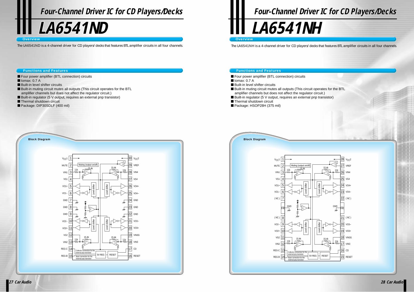
LA6541NDLA6541ND
30
29
28
27
26
25
24
17
23
22
21
20
19
18
16
1
2
3
4
5
6
7
11k
+-
+-
+-
+-
11k15.4k 15.4k
11k 11k15.4k 15.4k
5V REG RESET
VCC2
VREF
VIN4
VG4
VO4+
VO3+
GND
GND
GND
VIN3G
VIN3
CD
RESET
VO4-
VO3-
VCC1
MUTE
VIN1
VG1
VO1+
GND
GND
GND
VO2+
VG2
VIN2
REG-C
REG-B
VO1-
VO2-
14
8
9
10
11
12
13
15
27 Car Audio 28 Car Audio
LA6541NMLA6541NH
14
1
2
3
4
5
6
7
8
9
10
11
12
13
FR
15
28
27
26
25
24
23
22
21
20
19
18
17
16
FR
11k 11k15.4k 15.4k
11k 11k15.4k 15.4k
5V REG RESET
GND GND
VCC2
VREF
VIN4
VG4
VO4+
VO3+
VIN3G
VIN3
CD
RESET
( NC )
( NC )
VO4-
VO3-
VCC1
MUTE
VIN1
VG1
VO1+
VO2+
VG2
VIN2
REG-C
REG-B
( NC )
( NC )
VO1-
VO2-
Four-Channel Driver IC for CD Players/DecksFour-Channel Driver IC for CD Players/Decks Four-Channel Driver IC for CD Players/DecksFour-Channel Driver IC for CD Players/Decks
The LA6541ND is a 4-channel driver for CD players/decks that features BTL amplifier circuits in all four channels.
Four power amplifier (BTL connection) circuits Iomax: 0.7 A Built-in level shifter circuits Built-in muting circuit mutes all outputs (This circuit operates for the BTL amplifier channels but does not affect the regulator circuit.) Built-in regulator (5 V output, requires an external pnp transistor) Thermal shutdown circuit Package: DIP30SDLF (400 mil)
Overview
Functions and Features
Overview
Functions and Features
Block Diagram Block Diagram
Muting (output on/off)
Leve
l shi
fter
Leve
l shi
fter
Leve
l shi
fter
Leve
l shi
fter
Collector connection for the external pnp transistor
Base connection for the external pnp transistor
Muting (output on/off)
Leve
l shi
fter
Leve
l shi
fter
Leve
l shi
fter
Leve
l shi
fter
Collector connection for the external pnp transistor
Base connection for the external pnp transistor
The LA6541NH is a 4-channel driver for CD players/decks that features BTL amplifier circuits in all four channels.
Four power amplifier (BTL connection) circuits Iomax: 0.7 A Built-in level shifter circuits Built-in muting circuit mutes all outputs (This circuit operates for the BTL amplifier channels but does not affect the regulator circuit.) Built-in regulator (5 V output, requires an external pnp transistor) Thermal shutdown circuit Package: HSOP28H (375 mil)
+-
+-
+-
+-
+-
+-
+-
+-

LA6548NHLA6548ND LA6548NHLA6548ND
14
1
2
3
4
5
6
7
8
9
10
11
12
13
FR
15
28
27
26
25
24
23
22
21
20
19
18
17
16
FR
11k 11k15.4k 15.4k
11k 11k15.4k 15.4k
3.3V REG RESET
GND GND
VCC2
VREF
VIN4
VG4
VO4+
VO3+
VG3
VIN3
CD
RESET
( NC )
( NC )
VO4-
VO3-
VCC1
MUTE
VIN1
VG1
VO1+
VO2+
VG2
VIN2
REG-C
REG-B
( NC )
( NC )
VO1-
VO2-
30
29
28
27
26
25
24
17
23
22
21
20
19
18
16
1
2
3
4
5
6
7
11k 11k15.4k 15.4k
11k 11k15.4k 15.4k
RESET
VCC2
VREF
VIN4
VG4
VO4+
VO3+
GND
GND
GND
VIN3G
VIN3
CD
RESET
VO4-
VO3-
VCC1
MUTE
VIN1
VG1
VO1+
GND
GND
GND
VO2+
VG2
VIN2
REG-C
REG-B
VO1-
VO2-
14
8
9
10
11
12
13
15
29 Car Audio 30 Car Audio
Block Diagram Block Diagram
Muting (output on/off)
Leve
l shi
fter
Leve
l shi
fter
Leve
l shi
fter
Leve
l shi
fter
Collector connection for the external pnp transistor
Base connection for the external pnp transistor
Muting (output on/off)
Leve
l shi
fter
Leve
l shi
fter
Leve
l shi
fter
Leve
l shi
fter
Collector connection for the external pnp transistor
Base connection for the external pnp transistor
Four-Channel Driver IC for CD Players/DecksFour-Channel Driver IC for CD Players/Decks Four-Channel Driver IC for CD Players/DecksFour-Channel Driver IC for CD Players/Decks
Overview
Functions and Features
Overview
Functions and Features
Four power amplifier (BTL connection) circuits Iomax: 0.7 A Built-in level shifter circuits Built-in muting circuit mutes all outputs (This circuit operates for the BTL amplifier channels but does not affect the regulator circuit.) Built-in regulator (3.3 V output, requires an external pnp transistor) Thermal shutdown circuit Package: DIP30SDLF (400 mil)
Four power amplifier (BTL connection) circuits Iomax: 0.7 A Built-in level shifter circuits Built-in muting circuit mutes all outputs (This circuit operates for the BTL amplifier channels but does not affect the regulator circuit.) Built-in regulator (3.3 V output, requires an external pnp transistor) Thermal shutdown circuit Package: HSOP28H (375 mil)
The LA6548ND is a 4-channel driver for CD players/decks that features BTL amplifier circuits in all four channels. The LA6548NH is a 4-channel driver for CD players/decks that features BTL amplifier circuits in all four channels.
3.3V REG
+-
+-
+-
+-
+-
+-
+-
+-
+-
+-
+-
+-

LA6565LA6565
19
20
21
22
23
24
25
26
27
RF
28
29
30
31
32
33
34
35
36
18
17
16
15
14
13
12
11
10
RF
9
8
7
6
5
4
3
2
1
44k
44k
11k
11k
44k11k
11k44k
CH1
SGND
VCONT
MUTE234
MUTE1
VIN4-
VIN4
VREF-IN
VREF-OUT
REG-OUT
REG-OUT
VIN+OP
VIN-OP
VIN3
VIN3-
VIN2-
VIN2
VIN2+
VO-OP
FWD
REV
VLO-
VCCP2
VLO+
VO4+
VO4-
VO3+
VO3-
VO2+
VO2-
VO1-
VCCP1
VCCS
VIN1-
VIN1+
VIN1
VO1+
CH2,3,4
(VDD)REGIN
REGOUT
31 Car Audio 32 Car Audio
LV8280TLV8280T
+-
+-
+-
+-
+
RF
WOUT
VCTL
VOUT
UOUT
VS
COM
VCCVG
CP1
CPC
1
VCR
EF
+
FIL
CO
MIN
VCO
RM
AX
RM
IN
VCO
IN
FG
BRK
S/S
VCO OSC
VREF
TSD
Block Diagram Block Diagram
Overview
Functions and Features
Overview
Functions and Features
Five-Channel Driver IC for CD Players/DecksFive-Channel Driver IC for CD Players/Decks
The LA6565 is a 5-channel driver for CD players/decks that features BTL amplifier circuits in four channels plus a single H-bridge driver circuit.
Five power amplifier circuits (bridge connection (BTL connection): 4 channels, H bridge: 1 channel) Iomax: 1 A Built-in level shifter circuits (except for the H-bridge channel) Built-in muting circuits (two systems) mute all outputs (This circuit operates for the BTL amplifier channels but does not affect H-bridge and the regulator circuit.) Built-in regulator (requires an external pnp transistor and is set with an external resistor) Output voltage setting function (for the loading motor channel) Thermal shutdown circuit Package: HSOP36R (375 mil)
DVD-ROM Spindle Motor Driver IC
The LV8280T is a sensorless motor driver IC that provides a reverse torque braking function and is appropriate as the spindle motor driver in CD-ROM/DVD players. This IC adopts a direct PWM drive technique and uses a MOSFET as the output transistor for high-efficiency motor drive.Since this IC can implement motor drive without the use of a Hall effect device, it can be effective in supporting motor system miniaturization, thinner form factors, and reduced power consumption.
Three-phase full-wave sensorless motor driver Direct PWM drive (low side control) MOSFET output Synchronous commutation Supports switching between reverse torque braking and short-circuit braking Voltage controlled amplifier Analog input, PWM output FG output (Two outputs: single Hall device equivalent FG and three Hall device equivalent FG outputs) Current limiter circuit Thermal protection circuit Standby mode power saving circuit Package: TSSOP30 (275 mil)
DVD-ROM Spindle Motor Driver IC
Input
Thermal shutdowncircuit
Signal system ground
(Loading motor driver output voltage setting)
MutingControls the on/off state of the corresponding channel.
Out
put c
ontro
l
High: output on, low: output off
Leve
l shi
fter
Leve
l shi
fter
Leve
l shi
fter
Leve
l shi
fter
Power systemground
Signal system power supply
To VREFOUT
To VREFOUT
Pow
er s
yste
mgr
ound
Chargepump
Sensorlessdrive logic
Commutationlogic
Phasecomparator
Waveformsynthesis
+- +
-
+-
+-
+-
+-
+-
+-
+-
+
+
-
-
+-
+-

33Car Audio 34 Car Audio
LV8222WLV8222W
PRE DRIVELOGIC
VS1
PGND1
MUTE
VSMON
CLK
CP1
CPC1
CP2
CPC2
GN
D
VG
VGR
EG FG S/S
BRK
MO
DE1
MO
DE2
PWM
VCC
WOUT
FR
VS
COM
COMIN
FIL
VCORMAX
OU
T3F
IN3R
IN3F
PGN
D2
VS2
OU
T2R
IN2R
IN2F
OU
T1R
OU
T1F
IN1R
IN1F
VS3
VCOIN
VOUTUOUT
PRE DRIVELOGIC PRE DRIVELOGIC
OU
T2F
OU
T3R
PGND3
0.19V
1/2VSMON
OSC
1/N
1/N
SEL
VGREG
VCO
PRE DRIVE
LV8212TLV8212T
LOG
ICLO
GIC
PRE
DR
IVE
PRE
DR
IVE
LOG
ICLO
GIC
LOG
IC
S R
Q
S R
Q
S R
Q
CH
ARG
EPU
MP
1/N
OSC
1
AREF
AREF
AREF
OSC
2
TSD
SEN
SOR
LESS
LOG
IC
SPIN
DLE
PRED
RIV
E
VREF
OSC
SELE
CTO
R
OUT1R
VSI
OUT1F
OUT2FPGND1
OUT3R
OUT3FPGND3
PGND4RF4
VS4
VS3
OUT4F
OUT5F
OUT5R
OUT2R
OUT4R
SPR
FSP
GN
D
WO
UT
VOU
TU
OU
T
SPVS
SPC
OM
SPFI
LSP
CIN
OSC BR
K
S/S
CF3 IN
3
CF2 IN
2
IN1
MU
TECF1
PGN
D5
RF5
IN5
IN4
PCCPC
VGVCTL
SREF
AREF
GSW
VCC
GND
1FG
3FG
SUB
PRE
DR
IVE
PRE
DR
IVE
PRE
DR
IVE
The LV8222W is a system motor driver IC that integrates, on a single chip, all the motor driver circuits required by CD and MD players. Since this IC provide both a 3-phase PWM spindle motor driver and sled, focus, and tracking drivers (3 PWM H-bridge driver channels), it can contribute to end product motor system miniaturization,thinner form factors, and reduced power consumption.Since the spindle motor driver adopts a direct PWM sensorless drive technique, it provides high-efficiency motor drive with a minimal number of external components.
Direct PWM drive Three-phase full-wave sensorless motor driver (spindle block) Reverse torque braking (spindle block) MOS output transistors Standby mode power saving function Digital inputs, PWM outputs (spindle, sled, focus, and tracking) FG output VS voltage detection function Current limiter circuit Thermal protection circuit Package: SQFP48 (7 7 mm)
System Motor Driver IC for CD and DVD PlayersSystem Motor Driver IC for CD and DVD PlayersSystem Motor Driver IC for CD and MD PlayersSystem Motor Driver IC for CD and MD Players
Direct PWM drive (low side control) Three-phase full-wave sensorless motor driver (spindle block) Soft switching drive (spindle block) Synchronous commutation drive circuit Supports switching between reverse torque braking and short-circuit braking (spindle block) Analog input, PWM output (focus, tracking, sled, and spindle) Current control adopted in the sled block (channels 4 and 5) MOS output transistors Standby mode power saving function FG output (Two outputs: single Hall device equivalent FG (1FG) and three Hall device equivalent FG (3FG) outputs) Current limiter circuit Thermal protection circuit
The LV8212T is a system motor driver IC that integrates, on a single chip, all the motor driver circuits required by CD and DVD players. Since this IC provide not only a spindle motor driver, but also sled, focus, and tracking motor drivers (H-bridge drivers) for a total of 5 driver channels, it can contribute to end product motor system miniaturization and thinner form factors. Since the spindle motor driver adopts a direct PWM sensorless drive technique, it provides high-efficiency motor drive with a minimal number of external components.
Block Diagram Block Diagram
Overview
Functions and Features
Overview
Functions and Features
Sensorless drive logic
Phasecomparator
Chargepump
VGlimiter
Waveformsynthesis
Package: TQFP64J (7 7 mm)

.............Under development
35 Car Audio 36 Car Audio
P37
P37P37
P44 to 46
P40
P38 P44P47
P40
P48P45
P46P39
Extensive lineup provides full support for a wide range of systems
Car Audio Built-in PLL Tuner System Chipsets (1)
Analog block
Microcontroller single-chip car tuner with on-chip PLL circuit LV25200M
FM front end
Digital block
E2PROM
FM-IFdemodulator
FM/AM noisecanceler
SensorSW
AM tuner(double conversion)
MRC(multipath
reject circuit)
FM-MPXstereo
demodulation
CCB*bus interface
9-bit 1-channelD/A converter
PLL•AM double-conversion support circuit•High-speed lockup circuit•Dead zone control•Oscillator division circuit
LC875 Series
MicrocontrollerLCD driversVFD drivers
Loutput
Routput
Externalamplifier
Line amplifierLA2901V
Surroundprocessor ICs
LA2657M*(built-in electronic volume)
LA2655V*ConditionalProducts LC75410E/W
LC75411E/W
LC75412E/W
Electronicvolume with
new zero-crossmuting circuits
LA47536
LA47510
AF poweramplifier
Testinstrument
(GP-IB)
Processline computer
(PC)
Microcontroller Tuner IC Microcontroller Single-Chip Car Tuner with On-Chip PLL Circuit LV25200M
•No external FM RF amplifier required•Adjacent channel noise reduction variable band filter•AM noise canceller•Tuner supports all broadcast band standards used worldwide•Meets the new FCC regulations•Tuner specifications can be modified by changing the microprocessor software•Auto-adjustment system Automatic adjustment achieved by connecting the line computer and the E2PROM through the microprocessor•Best receiving system Optimizes the tuner functions in real time according to the reception conditions•Improved performance and reliability, circuit simplification, and design standardization achieved by the adoption of a microprocessor controlled tuner•On-chip PLL circuit•Package: QFP80 (14 14)
•Built-in differential input amplifiers (LC75410E/W, LC75412E/W)•Zero-cross muting•Input gain control•Loudness control•Package: (LC75410E) QIP64E (14 14) (LC75410W) SQFP64 (10 10) (LC75411E) QIP44M (10 10) (LC75411W) SQFP48 (7 7) (LC75412E) QIP64E (14 14) (LC75412W) SQFP64 (10 10)
•Provides a high output voltage of 5.3 V rms (with a THD of 0.1%) for improved signal-to- noise ratio when driving an external power amplifier•Low output noise voltage: 12 µV•Low total harmonic distortion: 0.005%•Superb audio fidelity•Package: SSOP24 (275mil)
Line Amplifier Four-Channel High Output Preamplifier IC LA2901V
Car Audio Built-in PLL Tuner System Chipsets (1)Car Audio Built-in PLL
Tuner System Chipsets (1)
AM/FM Tuner Block
SANYO has now added a PLL circuit to their original-design single-chip tuner IC.Microcontroller control provides increased performance and reliability and fewer adjustments in tuner systems.
SANYO has now added a PLL circuit to their original-design single-chip tuner IC.Microcontroller control provides increased performance and reliability and fewer adjustments in tuner systems.
For Automotive AV Equipment
P1 to 2 P1 to 2
P23 to 26
P1 to 2
P3
P4
P4 . P20
P6 . 21
P6 . 21
P5 . 22
P5
P5
LAN drivers
CARNETLA2330WLA2333TLA2351M
LA2360MLA2361AMLA2361JM
LA2340MLV2341M
CAN MOST
Electronic Volume Control Single-Chip Electronic Volume Control with New Zero-Cross Muting Circuit LC75410E/W, LC75411E/W, LC75412E/W
Varactor diodes for AM tuningSVC354 (3 diodes), SVC364 (4 diodes), SVC371 (6 diodes)Varactor diodes for FM tuningSVC230 (CR (C2.0V/C8.0V) ≥1.65, Q≥100)SVC243 (CR (C1.0V/C6.5V) ≥7.0, Q ≥40)SVC272 (CR (C2.0V/C8.0V) ≥2.3, Q ≥150)
SVC273 (CR (C2.0V/C8.0V) ≥3.1, Q ≥100)*: SV272, SV273: MCPH3 miniature package (2.1 2.0 mm) JFET and transistors for AMP amplifiersCPH5901 (high gain, typ 50 ms), CPH5905 (High ESD resistance type)Dual gate MOSFETs for FM amplifiers3SK263 (VDS = 15 Vmin, IDSX = 2.4 to 24 mA, yfs = typ 14 ms),3SK264 (VDS = 15 V, IDSX = 5.0 to 24 mA, yfs = typ 17 ms)
Transistors for AM and FM buffers 2SC2812N (VCEO = 50 V, IC = 150 mA, fT = typ 100 MHz),2SC2814 (VCEO = 20 V, IC = 30 mA, fT = typ 320 MHz)PIN diodes for AM AGC and switchingSeries with rs = typ 5 Ω: ISV247, ISV233, ISV246, ISV234, CPH5512PIN diodes for FM AGC and switchingSeries with rs = typ 6 Ω: ISV294, ISV315, ISV316, ISV298H
Other transistors (power supply, interface, and switch drive)Bipolar transistors: 50C02CH (VCEO = 15 V, IC=1 A, VCE (sat) = max 280 mV)(NPN) 2SC5706 ( VCEO = 50 V, IC = 5 A, VCES (sat) = typ 90 mV) 2SD1913 (VCEO = 60 V, IC = 3 A, PC = 20 W, hFE 70 to 280)MOSFET: 5LN 01M (VDSS = 50 V, ID = 100 mA RDS (on)(Nch) <VGS = 2.5 V> = 9.9 Ω) CPH6424 (VDSS = 60 V, ID = 3 A RDS (on) <VGS = 4 V> typ 150 mΩ)
All products described in this catalog contain developed products or products that are diverted from general types. In accordance with standard of quality management system ISO/TS16949 for automotive industry, there is a case where all demanded articles couldn't be supported, so please confirm to the salesman of our company at every order.
CCB
CCB
CCB is a SANYO’s original bus format and all the bus addresses are controlled by SANYO.
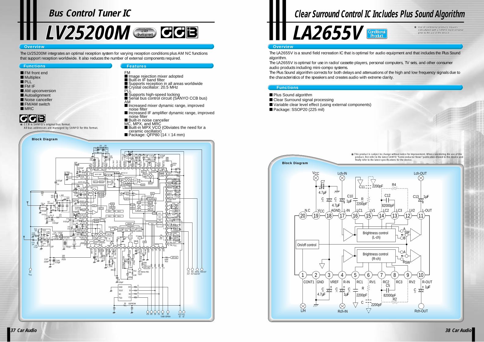
LV25200MLV25200M
1 2 3 4 5 6 7 8 9 10 11 12 13 14 15 16 17 18 19 20
60 59 58 57 56 55 54 53 52 51 50 49 48 47 46 45 44 43 42 41
40
39
38
37
36
35
34
33
32
31
30
29
28
27
26
25
24
23
22
21
61
62
63
64
65
66
67
68
69
70
71
72
73
74
75
76
77
78
79
80
+
+
+
+
+
+ +
++
+
+
+
0.01µF
1µF 0.47
µF
0.015µF
18pF
220pF
18pF
0.02
2µF
0.03
9 µF
0.22
µF
R103
100 C2 C4
C6 C7
8VVCC
SVC203
C103
12P18P 1P
6P
C1062200PC105
2200P
C1072200P
C10
4
C101
C102L102 L103
L104
R1022.2k
R101330
ANT
D
GN
D
IN2
OSC
-GN
D
FM O
SC
CPA
M
TEST
sep
adj.
GN
D CE DI
CL
DO3V
AM-M
IX
RF
AGC
2p 3p
1000p
4700
p
VCD_OSC
L_OSC
30K R12
C8
C9A
R11
C11
B
C12
B
C12 C15
C10
A
SD Stereo IND.TEST
100KR13
2.4K
6.8K
100KR20
0 0 0 0
0
0
0
0
30
p11 up
p11 up
CECS DI CL DOTUNER
DOEEPROM
EEPROM
VCC25V
X' TAL VCC
X TAL OUT
L-OUTR-OUT
SNC
X TAL INX' TAL GND
VCC5V
LchOUT
RchOUT
AM-NCGate-OUT
RDS-OUT
C2220.5M
C23
C25
0.015µF
0.22µF
0.47µF
0.47µF
2200p
0.22µF0.47µF
1U1U
10U
0.1µF
0.022µF
0.22
µF
0.022µF
0.022µF
0.022µF
10µF
0.47U
0.22U1U
C26
C27
C29
C30
C34
C35
C36
R38
VDD
HCC
R28
R29
R31
82K15K
3K
1U
1U
GNDTriger OUTAM NC
AM/FM
PLL-INMPXCHCC
SENC
AGCNOISE
VSM
MRC-OUTVSM-2
NOISE10K
R37C37
C38
C39
1M
1000p
R40
R41
C40
C41
C42C43C46C47
C51
C574.7U
C50
C44C48
C491000p
68K
MR
C IN
DR
IVE
MU
TEAF
C IN
VREF
DET
OU
T
NC-IN
IND
EXM
OD
Det
-out
Und
esire
RO
S-O
UT
PLL
TEST
PLL
TEST
AMC
L
IF A
GC
AM-W
-AG
C
BYPA
SSR
F-AG
CIF
-INAM PI
LOT-
DET
V CC
R43R47
10K 3300p
8200
p
0.02
U
C50B
10K
10K10K
R55
R56R57C
C56
C59
C61
C62
C58
C69
C67
0.022µF
0.022µF
0.022µF
0.022µF
0.022µF
0.025µF
0.047µF0.47µF
0.075µF
L1010.22µF
C71
C74C78
C73
C3547U
C75
C77
C79
C80
1000P
1000P
C105
30P
3.3U
3.3U
450K
1U
AMIF-IN2
FM-IF-IN2
FM-IF-IN
AM RF-AGC
AM-MI 2
AM-MI 2
AM-MI 2-IN
BYPASSRF-DAC
IF-INBIAS
FM1stIF-INTEST
AM-ANT-D
N-AGCMIX-OUT
MIX-OUTFE-VCC
FM-MIX-IN
INFM-MIX
INFM-MIX
1ST-IF-OUT
OUTVref4.9V
10.7MS3
10.7MS3
32KR70
R77
300
470
100K
R73
Lodins coil
1SV234
FM cut
R6675 R58
620
FETCPH5905
ANT D RF AGC
IQ MIX
MIXAM
1/10.1/8div1/6.1/4
div
IN1/IN2
OSC BUFFER
FM OSC
3K CP1
swallowcounter
orogramabledivider
ohasedetector
referencecounter
Vref 3V
SD Stereo
Vo1.
OSC
busMATRIX
SNC
HCC
Subdecorder
P-CAN
38K<0
19K<0
19K<90
FF
BUFF
TRIG
P-DETPhase
MPX VCC
GateTrig
AGC
anp
+
+
-
-
+-
+-+
-
LPF
HPF
select
8bit AD
IN3-3
IN3-4
IN3-1
IN3-2
ANT d
DAC
Keyed AGCN AGCW AGC
reg4.9V N AGCRF AGCW AGC
MIX
AM IF AMP
NC in Gtime
det
IF AGC
AM low cut
MIX
s-meter Mutedelay
Time
N amcAFCQD
rey2.7V
MuteAMP
BPF
Ccont
GND DO
TEST DI
NC SK
VDD CS
C109
37 Car Audio 38 Car Audio
LA2655VLA2655V
4.7µF
1 2 3 4 5 6 7 8 9 10
20 19 18 17 16 15 14 13 12 11
+ +
+
+
+
+CONT1 GND VREF R-IN RC1 RC2 RC3RV1 RV2 R-OUT
C C1µF
1µF
2200pF 82000pF
2200pF
CC5
R
R2C
4.7µF1µF
1µF
N.C AGND L-IN LC1 LC2 LC3LV1 LV2 L-OUTVCC
4.7µF
2200pF
2200pF
82000pF
C
C7
C10
C11
RC
C
L/H Rch-IN Rch-OUT
Lch-OUTLch-INVCC
BSW
A
A
B
(R-ch)
(L-ch)SW
C12
R4
C13
Pin_D
Pin_D
L_MI 2
L_AM3L_AM4
Pin_
D
CF10.7
CF10.7
L_MIX
500K
R8
Bus Control Tuner ICBus Control Tuner IC Clear Surround Control IC Includes Plus Sound AlgorithmClear Surround Control IC Includes Plus Sound Algorithm
: CCB is SANYO's original bus format. All bus addresses are managed by SANYO for this format.
The LV25200M integrates an optimal reception system for varying reception conditions plus AM NC functions that support reception worldwide. It also reduces the number of external components required.
FM front end Multiplex PLL FM IF AM upconversion Autoalignment Noise canceller FM/AM switch MRC
FM Image rejection mixer adopted Built-in IF band filter Supports reception in all areas worldwide Crystal oscillator: 20.5 MHzPLL Supports high-speed locking Serial bus control circuit (SANYO CCB bus)AM Increased mixer dynamic range, improved noise filter Increased IF amplifier dynamic range, improved noise filter Built-in noise cancellerMC, MPX, and MRC Built-in MPX VCO (Obviates the need for a ceramic oscillator) Package: QFP80 (14 14 mm)
FeaturesFunctions
Functions
Overview OverviewThe LA2655V is a sound field recreation IC that is optimal for audio equipment and that includes the Plus Sound algorithm.The LA2655V is optimal for use in radio/cassette players, personal computers, TV sets, and other consumer audio products including mini-compo systems.The Plus Sound algorithm corrects for both delays and attenuations of the high and low frequency signals due to the characteristics of the speakers and creates audio with extreme clarity.
Plus Sound algorithm Clear Surround signal processing Variable clear level effect (using external components) Package: SSOP20 (225 mil)
Block Diagram
Block Diagram
ConditionalProduct
ConditionalProduct
: Use of conditional products requires consultation with a SANYO representative prior to the use of the device.
: Use of conditional products requires consultation with a SANYO representative prior to the use of the device.
:This product is subject to change without notice for improvement. When considering the use of this product, first refer to the latest SANYO "Semiconductor News" publication related to this device and finally refer to the latest specifications for the device.
Brightness control
Brightness control
On/off control
Underdevelopment
Underdevelopment

LA2657MLA2657MLA2657M
17 18 19 20 21 22 23 24 25 26 27 28 29 30 31 32
64 63 62 61 60 59 58 57 56 55 54 52 51 50 49
48
47
46
45
44
43
42
41
40
39
38
37
36
35
34
33
1
2
3
4
5
6
7
8
9
10
11
12
13
14
15
16
NC
NC
VCC BBEon/off F.SW
NC
NC
NC
NC
NCNC
NC
EVR
EVR
NC
F.SW
PA
PAPA
PA+
+
+
++
+
+
VDD
CE DI CL53
BBE
BBE
BBE
BBE
+
+
+
+
+
+
+
+
+
F.SW
F.SW
Vreg
EVR
TONES-BASS
V ef
BBESW
BBE
BBE
CCBINTERFACE
FADER
FADERTONES-BASS
EVR
39 Car Audio 40 Car Audio
LA2901VLA2901VLA2901V
36kΩ
24kΩ
24kΩ
36kΩ
36kΩ
30kΩ
30kΩ
12kΩ
36kΩ
12kΩ
30kΩ
30kΩ
36kΩ
36kΩ
10kΩ10kΩ10kΩ10kΩ
24kΩ
24kΩ
+ +
22µF 22µF 47µF
LF-IN LR-IN
RippleFilter
+
22µF
22µF
RF-IN
+
22µF
RR-IN
+
DC
-R
DC
-L
--
--
+--+
-- +
+--+--+-- +-- +-- +
+
22µF
100µF
10µF
100µF
22µF 1.5NF1.5NF +
+
+
+
+
22µF
+
LF-OUT LR-OUTRF-OUT RR-OUT
VCC9.0V
VR
EF
VR
EF
VR
EF
VR
EF
VR
EF
VR
EF
VC
C
VC
C
VC
C
VC
C
SIG
NA
LA
MP
SIG
NA
LA
MP
LIF
TA
MPLIF
TA
MP
SIG
NA
LA
MP
SIG
NA
LA
MP
--+-- +-- +
1 2 3 4 5 6 7 8 9 10 11 12
24 23 22 21 20 19 18 17 16 15 14 13
XX
Four Channel High-Output Line Amplifier Four Channel High-Output Line Amplifier for Car Audiofor Car Audio
Car Audio Electronic Volume Control IC Car Audio Electronic Volume Control IC Car Audio Electronic Volume Control IC with BBE Surround Processorwith BBE Surround Processorwith BBE Surround Processor
Four Channel High-Output Line Amplifier for Car Audio
ConditionalProduct
ConditionalConditionalConditionalProductProductProduct
: Use of conditional products requires consultation with a SANYO representative prior to the use of the device.
OverviewOverview
Functions and FeaturesFunctions
Block Diagram Block Diagram
:This product is subject to change without notice for improvement. When considering the use of this product, first refer to the latest SANYO "Semiconductor News" publication related to this device and finally refer to the latest specifications for the device.
The LA2657M is an audio signal processor for car audio that integrates the functions of the LC75421 IC and a BBE surround processing on a single chip. The LA2657M's main functions include input functions, input gain adjustment, tone controls, super bass function, balance control, volume fader control, and the BBE surround processor.
Input functions: Four input systems (L+R) (The LC75421 provides five input systems.) Input gain control (0 to 18.75 dB in 1.25 dB steps) BBE processor Tone controls (Bass: ±11.9 dB, treble: ±11.9 dB. Both in 1.7 dB steps) Super bass (0 to 20 dB in 2 dB steps) Master volume control (0 dB to -79 dB in 1 dB steps, -∞) Bus control Fader (0 to -20 dB in 2 dB steps, -20 to -25 dB in 5 dB steps, -25 to -45 dB in 10 dB steps, -60 dB, -∞) CCB bus (On/off control of the BEE function is not provided over the CCB bus.) Package: QIP64E (14 14 mm)
The LA2901V is a 4-channel high-output line amplifier designed for car audio applications.Since the output voltage is increased significantly over conventional line amplifiers, the LA2901V achieves a high signal-to-noise ratio and high audio quality in the connection from the main unit to the external amplifier and can improve power amplifier performance.The LA2901V also provides significant space savings over earlier solution but reducing by one half the number of capacitors previously required to boost the signal system supply voltage and by adopting the SSOP miniature package.
High output level (5.3 V rms) Low output noise voltage (12 µV) Low total harmonic distortion (0.004 %) High ripple rejection ratio (70 dB) Minimal number of external components required Superb audio quality Package: SSOP24 (275 mil)
We recommend the use of 1% tolerance or better resistors for the 24 kΩ and 36 kΩ feedback resistors.
BBE and BBE symbol are registered trademarks of BBE Sound, Inc.R

.............Under development
41 Car Audio 42 Car Audio
P38P44
P47
P48P45
P46P39
P43 P43
P39
P44,P45,P46
Extensive lineup provides full support for a wide range of systems
For Automotive AV Equipment
P23 to 26
Car Audio Built-in PLL Tuner System Chipsets (2)Car Audio Built-in PLL
Tuner System Chipsets (2)Car Audio Built-in PLL
Tuner System Chipsets (2)
CCB
CCB
FM front endFM-IF
demodulatorFM/AM noise
canceler
AM tuner(double conversion)
MRC(multipath
reject circuit)
FM-MPXstereo
demodulation
LC875 Series
Microcontroller
Surroundprocessor ICs
LA2655V*ConditionalProducts
LA2657M*(built-in electronic volume)
LC75410E/W
LC75411E/W
LC75412E/W
Electronicvolume with
new zero-crossmuting circuits
LA47510
LA47536
AF poweramplifier
CCB is a SANYO’s original bus format and all thebus addresses are controlled by SANYO.
Complete car tuner with on-chip PLL circuitLA17000M
VT VCO 2nd OSC
PLL synthesizerLC72144Mequivalent
PLL synthesizer
Car Audio Single-Chip Tuner Complete Car Tuner with Built-in PLL Circuit LA17000M
Built-in PLL circuit•A/D converter (6 bits, 1 channel)•Includes an IF counter and I/O ports for simplified interfacing•Adopts an AM double conversion reception techniqueFurther improved to noise reduction•Superlative three-signal characteristics•Improved medium and weak field NC characteristics•Improved separation characteristics•Built-in anti-birdie filter•Multipath sensor outputs (analog and digital outputs)Support for lower total system costs•AM double-conversion (up-conversion system)•Improved FM IF circuit (automatic wide/narrow CF switching with software in the presence of adjacent channel interference)•Reduction in sample-to-sample IF gain variations by 1/3 simplifies adjustments during manufacturingSupports end-product miniaturization•High-frequency signal lines can be handled inside the tuner pack•Easily meets the new FCC regulationsPackage: QFP80 (14 14)
BBE Sound Processor IC LA2657M*
Electronic Volume Control Single-Chip Electronic Volume Control with New Zero-cross Muting Circuit LC75410E/W, LC75411E/W, LC75412E/W
•Input function•Input gain control•BBE•Tone and balance controls•Super bass•Master volume control•Fader•CCB support•Package: QFP64E (14 14)
•Built-in differential input amplifiers (LC75410E/W, LC75412E/W)•Zero-cross muting•Input gain control•Loudness control•Package: (LC75410E) QIP64E (14 14) (LC75410W) SQFP64 (10 10) (LC75411E) QIP44M (10 10) (LC75411W) SQFP48 (7 7) (LC75412E) QIP64E (14 14) (LC75412W) SQFP64 (10 10)
AM/FM Tuner Block
LCD driversVFD drivers
Requires a priori consultation with your SANYO sales representative or SANYO business office before their use.
BBE and BBE symbol are registered trademarks of BBE Sound, Inc.
SANYO has now added a PLL circuit to their original-design single-chip tuner IC.The optimum chip segmentation realized high-performance, unadjusted, and high-reliability of car tuner systems at low costs.
*
SANYO has now added a PLL circuit to their original-design single-chip tuner IC.The optimum chip segmentation realized high-performance, unadjusted, and high-reliability of car tuner systems at low costs.
Loutput
Routput
P1 to 2 P1 to 2 P1 to 2
P3
P4
P4 . P20
P6 . 21
P6 . 21
P5 . 22
P5
P5
LAN drivers
CARNETLA2330WLA2333TLA2351M
LA2360MLA2361AMLA2361JM
LA2340MLV2341M
CAN MOST
Varactor diodes for AM tuningSVC354 (3 diodes), SVC364 (4 diodes), SVC371 (6 diodes)Varactor diodes for FM tuningSVC230 (CR (C2.0V/C8.0V) ≥1.65, Q≥100)SVC243 (CR (C1.0V/C6.5V) ≥7.0, Q ≥40)SVC272 (CR (C2.0V/C8.0V) ≥2.3, Q ≥150)
SVC273 (CR (C2.0V/C8.0V) ≥3.1, Q ≥100)*: SV272, SV273: MCPH3 miniature package (2.1 2.0 mm) JFET and transistors for AMP amplifiersCPH5901 (high gain, typ 50 ms), CPH5905 (High ESD resistance type)Dual gate MOSFETs for FM amplifiers3SK263 (VDS = 15 Vmin, IDSX = 2.4 to 24 mA, yfs = typ 14 ms),3SK264 (VDS = 15 V, IDSX = 5.0 to 24 mA, yfs = typ 17 ms)
Transistors for AM and FM buffers 2SC2812N (VCEO = 50 V, IC = 150 mA, fT = typ 100 MHz),2SC2814 (VCEO = 20 V, IC = 30 mA, fT = typ 320 MHz)PIN diodes for AM AGC and switchingSeries with rs = typ 5 Ω: ISV247, ISV233, ISV246, ISV234, CPH5512PIN diodes for FM AGC and switchingSeries with rs = typ 6 Ω: ISV294, ISV315, ISV316, ISV298H
Other transistors (power supply, interface, and switch drive)Bipolar transistors: 50C02CH (VCEO = 15 V, IC=1 A, VCE (sat) = max 280 mV)(NPN) 2SC5706 ( VCEO = 50 V, IC = 5 A, VCES (sat) = typ 90 mV) 2SD1913 (VCEO = 60 V, IC = 3 A, PC = 20 W, hFE 70 to 280)MOSFET: 5LN 01M (VDSS = 50 V, ID = 100 mA RDS (on)(Nch) <VGS = 2.5 V> = 9.9 Ω) CPH6424 (VDSS = 60 V, ID = 3 A RDS (on) <VGS = 4 V> typ 150 mΩ)
All products described in this catalog contain developed products or products that are diverted from general types. In accordance with standard of quality management system ISO/TS16949 for automotive industry, there is a case where all demanded articles couldn't be supported, so please confirm to the salesman of our company at every order.

LA17000M LC75410E/WLC75410E/WLA17000M
1
FMANTD
ANTD
2
FM RFAGC
3
FEGND
4
FMOSC
5 6
AM/FMSW
7
AMOSC
8
NCSens
9
NCAGC
10
AMOSC
11
GoreOUT
12 13
MPXPdot IN
14
NC MPXGND
15 16 17
SDST-IND
18
PLL IN
19 20
PD1
41
AM/FMS-METER
4243
MRCOUT
44SNCHCCNC
454647
DETOUT
SEPADJ
48
FMS-METER
49
MUTEDRIVE
50
AFCIN
51
QDOUT
52
QDIN
53
VREF
54
FMSD
55
KEYEDAGC
56
VCC
57
C.HCC
58
AMLC
59
PILOTDET
60
IFAGC
21
PLLVSS
22PDS
23XBUFF
24I/O-2
25X' IN
26X' OUT
27CE
28DI
29CL
30DO
31I/O-1
32HCTR
33SEEKSW
34
35
36
37MPX VCO
38
IF COUNT BUFFSEEK/STOP Switch
CSB912TF108
39GND
40
PHASECOMP
61AM DET
62
AM ANTDWIDE AGC
63
FM MUTEON ADJ
64RF AGC
652nd MIX IN
66FM IF BYPASS
VSMSHIFTER
67
FM IFIN
68
691st IF OUT
70AM MIX OUT
71AM SD ADJ
WIDE AGC IN
721st IF IN
73AM RF AGC OUT
74
75
N-AGC INMUTE ATT ADJ
76MIX OUT
77FE VCC
78
1st IFNarrow IN
79
AM 1stMIX IN
80FMMIX IN
3.3µ
F
0.02
2µF
0.02
2µF
0.01
µF
0.47
µF
1 µF
0.01
µF
0.02
2µF
0.01
5µF
6800pF 0.01µF30kΩ
1MΩ
350Ω 51kΩ
30kΩ
10kΩ
22kΩ
51kΩ
10kΩ
11kΩ
300Ω
51kΩ
470Ω
100k
Ω
510Ω
33Ω
10kΩ
10kΩ
24kΩ
30kΩ
12kΩ
62kΩ
82kΩ
560Ω
56kΩ
33kΩ
33kΩ
1000
pF
10k Ω
50kΩ
5.6k
Ω
47kΩ
47kΩ
47kΩ
100kΩ
100k
Ω
51kΩ
5V
10kΩ
100k
Ω
10kΩ
10pF 300p
F
150p
F
100p
F
30pF
VCC=8V
FM A
NT
IN
5pF
AGC
HPH
HOLEDET
F.F.19k 90
PHASECOMP.
VCO
PILOTDET.
CCBI/F
POWERON
RESET
PHASEDETECTOR
CHARGEPUMP
F.F.19k 90
F.F.30k 0
F.F.
PILOTCAN.
UNTVERSALCOUNTER
DATA SHIFT REGISTERLATCH
12BitsPROGRAMMABLE
DIVIDER
SWALLOWCOUNTER
1/16,1/17 4Bits
REFERENCEDIVIDER
TRIG
HCC
SNC
VCOSTOP
OC-CDET
AFCCI AMP
LPF
TRIG GATE
+—
MIX
MIX
ANTD
OSCBUFF OSC Q.DET
MUTEAMP.
MUTEDRIVE
DET IFAGC
L.C.
BUFF
OSC
BUFF
AM1STOSC
BUFF
IF LIMITAMP.
KeyedAGC
MAINHC SUB
DECMATRIX
F.EREG
FM/AMSWITCH
AM/FMVREF
CFSW
W.B AGC
RF AGC
AM SM
AM SD
FM SM
FM SD
IF BUFFER
MRCRF AGCWB AGC
TWEET
+
+ +
+
++
+++
++
+
+
+
+
+
0.01
5µF
0.22µF
3.3µF
15pF
15pF
0.022µF
0.02
2µF
100µH
100µ
H0.
022 µ
F0.
022µ
F
47µF
FC18
100µH
1MH
0.022µF
1µF
0.02
2 µF
100 µ
F
+2.2µ
F
0.47µF
1µF
10µF
0.22
µF
2200
pF
0.1µ
F
0.47
µF
0.01
µF
0.22
µF
1 µF
1 µF
0.22
µF
1µF
0.47µF
0.01µF
0.022µF
Pdot CADJ
100pF
5V
24pF
24pF
10.25MHz
PLL VDD=5V
FM B
F G
ND
L-CHCF SW R-CH FMIF AMNCMPX VCC
FM/AMVT
FMIF AMGND
SEEK AM/FM SDSTOP FM ST INDSDSTSW
I/O-1
Tomicrocontroller
MUTEOFF(RDS)
AM(STEFEO)IF OUT
MRCSENORAUTO ADJ
+
30Ω
200kΩ
100Ω
100k
Ω10
0kΩ
220Ω
30kΩ
15Ω30Ω
100kΩ
150Ω
0.022µF
5pF
0.02
2µF
0.02
2µF
0.1µ
F
0.02
2µF
100µ
F
1000pF1000pF
37pF6pF
1000
pF
8pF
1000
pF
18pF
62pF
AM A
NT
IN
AM V
CC
49
48 47 46 45 44 43 42 41 40 39 38 37 36 35 34 33
32
31
+L5P
50+
L5M
51+
L4
52+
L3
+L2
54+
L1
55+
+
LVref
56
57
Vref
VDD
58
RVref
59+
R1
+R2
61+
R3
62+
R4
63+
R5M
64+
R5P
1µF
1µF
1µF
1µF
1µF
1µF
1µF
1µF
1µF
1µF
1µF
1µF
PA
10µF
1µF
LVref
LVre
f
10µF
47µF
+10µF
LSE
LO
LVR
IN
LCT
LCO
M
LTIN
LF1C
1
LF1C
2
LF1C
3
LF2C
3
LVR
OU
T
220pF
68kΩ
4.7kΩ 0.1µF
10µF0.1µ
F
0.1µ
F10µF 10µF
LF2C
1
LF2C
2
0.01
µF
0.01
µF
0.00
1µF
0.00
1µF
LF3C
3
LTO
UT
LF3C
1
LF3C
2
[BASS fo 100Hz] [ M I D fo 1kHz] [TREBLE fo 10kHz]
LFIN
LFOUT
30
29
28
PA
10µF
LROUT
LAVSS
TEST
PA
0.033µFRROUT
TIM
NC
18
19
21
20
17
PA
10µF
10µF
10µF10µF
10µFRFOUT
RFIN
16151413
RT
OU
T
RF
3C3
RF
3C2
RF
3C1
121110
RF
2C3
RF
2C2
RF
2C1
0.1µF
1µF
RVref
RV
ref
RV
ref
987
RF
1C3
RF
1C2
RF
1C1
6
RT
IN
5
RV
RO
UT
4
RC
OM
3
RC
T
2
RV
RIN
1
RS
ELO
27DVSS
26CL
25DI
24CE
47kΩ
23MUTE
22RAVSS
CL
DI
CE
RV
ref
NO SIGNALTIMER
ZERO-CROSS DET
ZERO-CROSS DET
CONTROLCIRCUIT
4.7kΩ68kΩ
220pF
60
LVre
f
LVre
f
53
0.1µ
F
0.1µ
F
0.01
µF
0.01
µF
0.00
1µF
0.00
1µF
Microcontroller
CCBINTERFACE
Multiplexer
Multiplexer
-+
-+
-+ +
+
+
-+
-+-+
+ + +
-+
-+
-+
+
+
-+
-+ -+
++
+
+
-+
-+
-+
LOGIC CIRCUIT
[BASS fo 100Hz] [ M I D fo 1kHz] [TREBLE fo 10kHz]
-+
-+
-+
-+
-+
-+
-+
43 Car Audio 44 Car Audio
The LA17000M is a car audio system tuner IC that integrates both a PLL frequency synthesizer and all AM/FM functions on a single chip. The LA17000M combines the functions of two ICs, a PLL IC (such as the LC72144) and an FM tuner IC (such as the LA1781M) on a single chip that provides PLL, AM (upconversion), FM FE, FM IF, NC, MCP, and MRC functions. The LA17000M achieves increased performance, adjustment-free manufacturing, and high reliability at low cost in car tuner systems by providing an optimal functional allocation in the IC.
Car Audio Tuner IC with Built-in PLL CircuitCar Audio Tuner IC with Built-in PLL Circuit
Built-in PLL A/D converter (6 bits, 1 channel) IF counter and I/O ports for simplified interface design Supports AM double conversion reception Strengthened noise reduction Superlative three-signal characteristics Improved weak and medium-field NC characteristics Improved separation characteristics Built-in anti-birdie filter (analog and digital outputs) Anti-multipath sensor outputs (analog and digital outputs)
Support for lower costs AM double conversion (upconversion) Improved FM IF circuit (automatic wide/narrow ceramic filter switching under adjacent channel interference conditions) IF gain sample-to-sample variations reduced to 1/3 that in previous devices. This simplifies end product adjustment during manufacture. Furthermore, a shifter pin is provided for VSM adjustment. Supports end product miniaturization High-frequency signal lines can be handled within the tuner pack. Easily meets FCC requirements Package: QFP80 (14 14 mm)
Mic
ro c
ontro
ller
Block Diagram
Block Diagram
The LC75410E/W is an electronic volume and tone control IC that implements a rich set of audio control functions with a minimal number of external components. Functions include volume, balance, fader, bass/midrange/treble, and loudness controls, as well as input selection/switching functions and an input gain control.
Electronic Volume and Tone Control IC for Car Audio SystemsElectronic Volume and Tone Control IC for Car Audio Systems
Overview Overview
Functions
Functions
Features
:CCB is SANYO's original bus format. All bus addresses are managed by SANYO for this format.
On-chip buffer amplifiers reduce the number of external components Internal switches are implemented in a silicon gate CMOS process that minimizes the noise generated when switching. This results in low noise even when switching in the no-signal state. Zero-cross switching circuits used for low noise even when input signals are present Built-in VDD/2 reference voltage generation circuit All functions are controlled using serial data (CCB) Packages: LC75410E: QIP64E (14 14 mm) LC75410W: SQFP64 (10 10 mm)
Volume control: A total of 161 positions from 0 dB to -79.5 dB in 0.5 dB steps and -∞ dB. A balance function can be implemented by controlling the left and right channel volume controls separately. Fader control: The rear or front outputs can be attenuated by one of 16 levels (A total of 16 settings with attenuations of 0 to -2 dB in 1dB steps, -2 to -20 dB in 2 dB steps, -20 to -30 dB in 10 dB steps, and -45, -60, and -∞ dB settings.) Bass/midrange/treble controls: Each band can be controlled in 1 dB steps from 0 dB to ±6 dB, and in 2 dB steps from ±8 dB to ±12 dB Input gain control: The input signal can be amplified by 0 to +18.75 dB in 1.25 dB steps Input switching: One of five input systems (left and right channels) can be selected (Four of the input systems are single-ended inputs, one uses differential inputs.) Loudness control: The -32 dB position of the 2 dB step volume control ladder resistor can be tapped and a loudness function implemented with external capacitor and resistor components

LC75412E/WLC75412E/WLC75411E/WLC75411E/W
L4
L3
L2
L1
Vref
VDD
R1
R2
R3
R4
1µF
1µF
1µF
1µF
PA
10µF
1µF
LVre
f
22µF
LSE
LO
LVR
IN
LCT
LCO
M
LTIN
LF1C
1
LF1C
2
LF1C
3
LF3C
1R
F3C
1
LVR
OU
T
220pF
68kΩ
4.7kΩ 0.1µF
10µF
10µF0.1µF0.1µF10µF
LTO
UT
[BASS fo 100Hz] [TREBLE]
LFIN
LFOUT
PA
10µF
LROUT
PA
0.033µFRROUT
TIM
TEST
PA
10µF
10µF
10µF10µF
10µFRFOUT
RFIN
RT
OU
T
0.1µF
1µF
RVref
RF
1C3
RF
1C2
RF
1C1
RT
IN
RV
RO
UT
RC
OM
RC
T
RV
RIN
RS
ELO
VSS
CL
DI
CE
VDD
CL
DI
CE
RV
ref
NO SIGNALTIMER
ZERO-CROSS DET
ZERO-CROSS DET
CONTROLCIRCUIT
4.7kΩ68kΩ
220pF
LVref
LVref
RVref
RVref
LVref
0.1µF2700pF
0.1µF
2700pF
MicroController
CCBINTERFACE
LOGIC CIRCUIT
Multiplexer
Multiplexer
+
+
+
+
+-
+-+-
+-
+-
+-+-
+-
+
+ ++
+
-
+-
++ + +
+
+
+
+
+-
+
+
+
+
+
[BASS fo 100Hz] [TREBLE]
+-
+-
+-
+-
+-
+-
+-
49
48 47 46 45 44 43 42 41 40 39 38 37 36 35 34 33
32
31
+
L5P
50
L5M
51
L4
52
L3
L2
54
L1
55
56
57
Vref
VDD
58
59
R1
R2
61
R3
62
R4
63
R5M
64
R5P
1µF
1µF
1µF
1µF
1µF
1µF
L61µF
1µF
R61µF
1µF
1µF
1µF
1µF
1µF
+PA
10µF
1µF
0.33µF
LVref
LVre
f
22µF
LSE
LO
LVR
IN
LCT
LF1C
1
LF1C
2
LF1C
3
NC
NC
NC
NC
NC
NC
1000pF 10kΩ
1kΩ
+
10µF0.1µ
F
0.1µ
F
0.00
1µF
0.00
1µF
LF3C
3
LTO
UT
LF3C
1
LF3C
2
[BASS fo 100Hz] [TREBLE fo 10kHz]
LFIN
LFOUT
30
29
28
+PA
10µF
LROUT
LAVSS
TEST
PA
0.033µFRROUT
TIM
NC
18
19
21
20
17
PA
10µF
10µF
10µFRFOUT
RFIN
16151413
RT
OU
T
RF
3C3
RF
3C2
RF
3C1
121110
0.33µF
1µF
RVref
RV
ref
RV
ref
987
RF
1C3
RF
1C2
RF
1C1
654
NC
NC
NC
NC
NC
NC
3
RC
T
2
RV
RIN
1
RS
ELO
27DVSS
26CL
25DI
24CE
47kΩ
1MΩ
23MUTE
22RAVSS
CL
DI
CE
RV
ref
NO SIGNALTIMER
ZERO-CROSS DET
ZERO-CROSS DET
CONTROLCIRCUIT
1kΩ10kΩ
1000pF
60
LVre
f
LVre
f
53
0.1µ
F
0.1µ
F
0.00
1µF
0.00
1µF
MicroController
LVref
RVref
+
+
+
+
+
+
+
+
+
+
+
+
+
+
+
+
+-
+
+-
+-
+
+
+-
+ +-
+-
+-
+-
-
+-
CCBINTERFACE
Multiplexer
Multiplexer
LOGIC CIRCUIT
[BASS fo 100Hz] [TREBLE fo 10kHz]
+-
+-
+-
+- +-
+-
45 Car Audio 46 Car Audio
Volume control: A total of 81 positions from 0 dB to -79 dB in 1 dB steps and -∞ dB. A balance function can be implemented by controlling the left and right channel volume controls separately. Fader control: The rear or front outputs can be attenuated by one of 16 levels (A total of 16 settings with attenuations of 0 to -2 dB in 1 dB steps, -2 to -20 dB in 2 dB steps, -20 to -30 dB in 10 dB steps, and -45, -60, and -∞ dB settings.) Bass/treble controls: Each band can be controlled in 2 dB steps from 0 dB to ±18 dB Input gain control: The input signal can be amplified by 0 to +18.75 dB in 1.25 dB steps Input switching: One of six input systems (left and right channels) can be selected (Five of the input systems are single- ended inputs, one uses differential inputs.) Loudness control: Taps are output starting at the -32 dB position of the ladder resistor and a loudness function implemented with external capacitor and resistor components
Overview
Functions
Features
Overview
Functions
Features
Electronic Volume and Tone Control IC for Car Audio SystemsElectronic Volume and Tone Control IC for Car Audio Systems
Electronic Volume and Tone Control IC for Car Audio SystemsElectronic Volume and Tone Control IC for Car Audio Systems
The LC75411E/W is an electronic volume and tone control IC that implements a rich set of audio control functions with a minimal number of external components. Functions include volume, balance, fader, bass/treble, and loudness controls, as well as input selection/switching functions and an input gain control.
On-chip buffer amplifiers reduce the number of external components Internal switches are implemented in a silicon gate CMOS process that minimizes the noise generated when switching. This results in low noise even when switching in the no-signal state Zero-cross switching circuits used for low noise even when input signals are present Built-in VDD/2 reference voltage generation circuit All functions are controlled using serial data (CCB) Packages: LC75411E: QIP44M (10 10 mm) LC75411W: SQFP48 (7 7 mm)
Volume control: A total of 161 positions from 0 dB to -79.5 dB in 0.5 dB steps and -∞ dB. A balance function can be implemented by controlling the left and right channel volume controls separately. Fader control: The rear or front outputs can be attenuated by one of 16 levels (A total of 16 settings with attenuations of 0 to -2 dB in 1 dB steps, -2 to -20 dB in 2 dB steps, -20 to -30 dB in 10 dB steps, and -45, -60, and -∞ dB settings.) Bass/treble controls: Each band can be controlled in 1 dB steps from 0 dB to ±6 dB, and in 2 dB steps from ±8 dB to ±12 dB Input gain control: The input signal can be amplified by 0 to +18.75 dB in 1.25 dB steps Input switching: One of 4 input systems (left and right channels) can be selected Loudness control: The -32 dB position of the 2 dB step volume control ladder resistor can be tapped and a loudness function implemented with external capacitor and resistor components
:CCB is SANYO's original bus format. All bus addresses are managed by SANYO for this format.
:CCB is SANYO's original bus format. All bus addresses are managed by SANYO for this format.
The LC75412E/W is an electronic volume and tone control IC that implements a rich set of audio control functions with a minimal number of external components. Functions include volume, balance, fader, bass/treble, and loudness controls, as well as input selection/switching functions and an input gain control.
On-chip buffer amplifiers reduce the number of external components Internal switches are implemented in a silicon gate CMOS process that minimizes the noise generated when switching. This results in low noise even when switching in the no-signal state Zero-cross switching circuits used for low noise even when input signals are present Built-in VDD/2 reference voltage generation circuit All functions are controlled using serial data (CCB) Packages: LC75412E: QIP64E (14 14 mm) LC75412W: SQFP64 (10 10 mm)
Block DiagramBlock Diagram
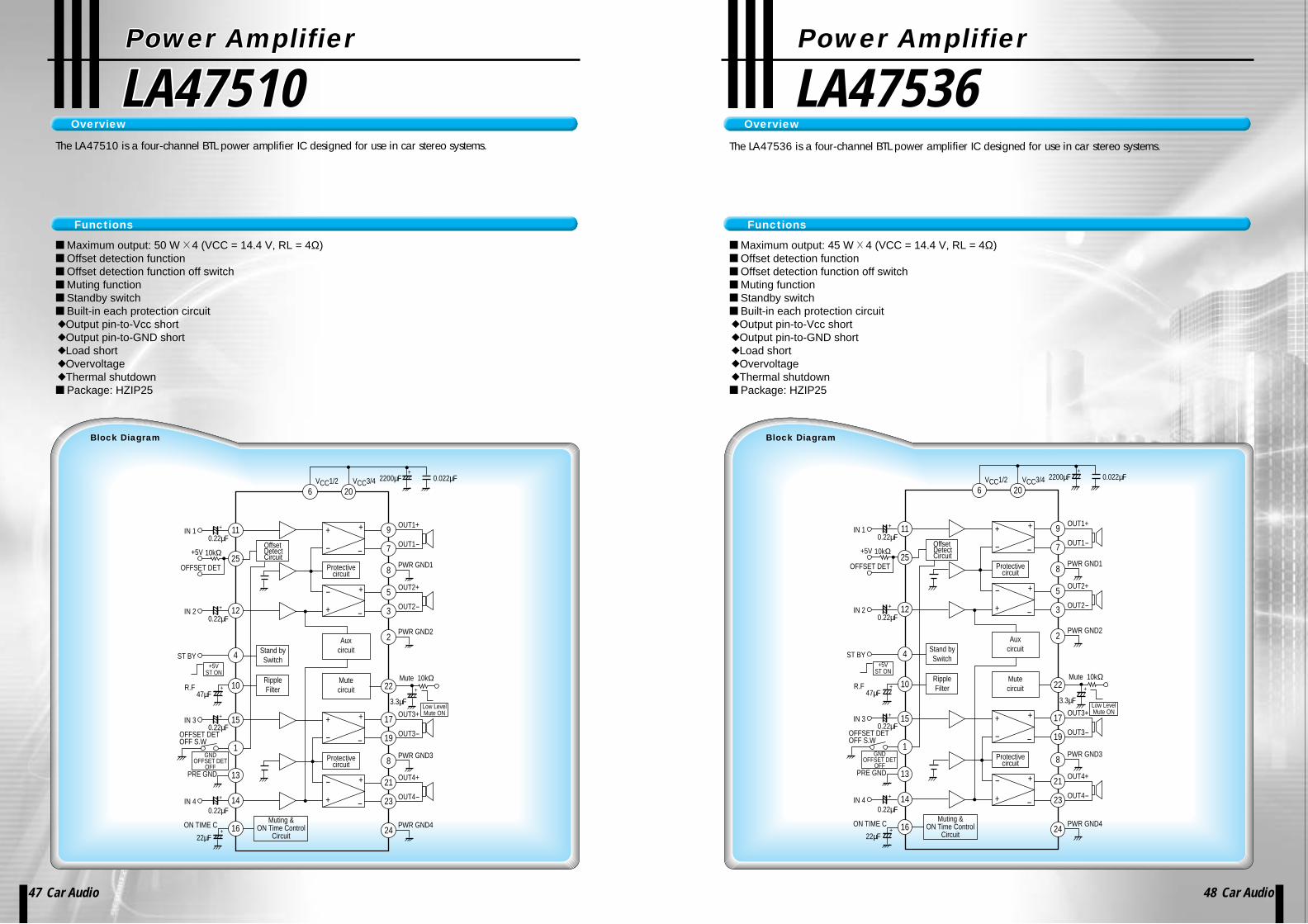
LA47510 LA47536LA47510 LA47536
16
14
13
1
15
10
4
12
25
11 9
7
8
6 20
++
- -
OUT1+
OUT1-
PWR GND1
5
3
+
+
-
-
OUT2+
OUT2-
17
19
++
+
-
-
-
OUT3+
OUT3-
21
23
+
-
OUT4+
OUT4-
+
2
22
PWR GND2
+
VCC1/2 VCC3/4 2200µF
+
+
22µF
0.22µF
3.3µF
0.022µF
Protectivecircuit
8PWR GND3
24PWR GND4ON TIME C
+47µF
R.F
PRE GND
IN 4
Protectivecircuit
+
0.22µFIN 3
ST BY
+
0.22µFIN 2
+
0.22µF
OFFSET DET
IN 1
Mute 10kΩ
Low LevelMute ON
+5VST ON
Auxcircuit
Mutecircuit
GNDOFFSET DET
OFF
OFFSET DETOFF S.W
+5V 10kΩOffsetDetectCircuit
Stand bySwitch
RippleFilter
Muting &ON Time Control
Circuit16
14
13
1
15
10
4
12
25
11 9
7
8
6 20
++
- -
OUT1+
OUT1-
PWR GND1
5
3
+
+
-
-
OUT2+
OUT2-
17
19
++
+
-
-
-
OUT3+
OUT3-
21
23
+
-
OUT4+
OUT4-
+
2
22
PWR GND2
+
VCC1/2 VCC3/4 2200µF
+
+
22µF
0.22µF
3.3µF
0.022µF
Protectivecircuit
8PWR GND3
24PWR GND4ON TIME C
+47µF
R.F
PRE GND
IN 4
Protectivecircuit
+
0.22µFIN 3
ST BY
+
0.22µFIN 2
+
0.22µF
OFFSET DET
IN 1
Mute 10kΩ
Low LevelMute ON
+5VST ON
Auxcircuit
Mutecircuit
GNDOFFSET DET
OFF
OFFSET DETOFF S.W
+5V 10kΩOffsetDetectCircuit
Stand bySwitch
RippleFilter
Muting &ON Time Control
Circuit
47 Car Audio 48 Car Audio
Overview
Functions
Overview
Functions
Power AmplifierPower Amplifier Power AmplifierPower Amplifier
Maximum output: 50 W 4 (VCC = 14.4 V, RL = 4Ω) Offset detection function Offset detection function off switch Muting function Standby switch Built-in each protection circuit Output pin-to-Vcc short Output pin-to-GND short Load short Overvoltage Thermal shutdown Package: HZIP25
The LA47510 is a four-channel BTL power amplifier IC designed for use in car stereo systems.
Maximum output: 45 W 4 (VCC = 14.4 V, RL = 4Ω) Offset detection function Offset detection function off switch Muting function Standby switch Built-in each protection circuit Output pin-to-Vcc short Output pin-to-GND short Load short Overvoltage Thermal shutdown Package: HZIP25
The LA47536 is a four-channel BTL power amplifier IC designed for use in car stereo systems.
Block DiagramBlock Diagram

.............Under development
.............New product
49 Car Audio 50 Car Audio
P44 to 46
P38
P47
P48
P39
P52P53
P54
P51
P51
P52
P53
P44
P40
P45
P46
For Automotive AV EquipmentCar Audio Standard Tuner System Chipsets
Extensive lineup provides full support for a wide range of systems
Surroundprocessor ICs
LA2655V*ConditionalProducts
LA2657M*(Built-in electronic volume control)
LC75410E/W
LC75411E/W
LC75412E/W
Electronicvolume with
new zero-crossmuting circuits
LA47510
LA47536
AF poweramplifier
Car Audio Single-Chip Tuner Single-Chip Tuner ICs for Car Audio LA1776M
Further improved noise reduction•Superlative three-signal characteristics•Improved medium and weak field NC characteristics•Improved separation characteristics•Built-in anti-birdie filterSupport for lower total system costs•AM double conversion (up-conversion system)•Sample-to-sample IF gain variations reduced by 1/3 from earlier Sanyo products, making adjustments during final product assembly significantly easier.Package: QIP64E (14 4)
ETR Controller Electronic Tuning Radio Controller LC72350 Series LC723780 Series
PLL•AM double-conversion support circuit•High-speed lockup circuit•Dead zone control•Oscillator division circuit
ROM: 16/24/32/64/128 KbytesRAM: 256/512/2048/4096/ 8192 bytes
Three externalinterrupt pins
A/D converter6-bit/8-bit 6 channels
8-bit serial I/O
Car audio bus controlled 1-chip tuner IC LA1776M
ETR controller LC72350 Series LC723780 SeriesLC72336 / LC72338
CCB
FM front end
AM tuner(double conversion)
MRC(multipath
reject circuit)
FM-IFdemodulator
FM-MPXstereo
demodulation
FM/AM noisecanceler
Line amplifierLA2901V
Externalamplifier
Loutput
R output
Large-capacity ROM: up to 128 KbytesHigh-speed operation:One machine cycle takes 1.33 µsHigh-performance built-in PLL•Direct PLL•High-speed lockup circuitPackage: (LC72350) QIP80E (14 20) (LC723780) QIP100E (14 20)
Electronic Volume Control Single-chip Electronic Volume Control with New Zero-cross Muting Circuit LC75410E/W, LC75411E/W LC75412E/W
Built-in differential input amplifiers (LC75410E/W, LC75412E/W)Zero-cross mutingInput gain controlLoudness controlPackage: (LC75410E) QIP64E (14 14) (LC75410W) SQFP64 (10 10) (LC75411E) QIP44M (10 10) (LC75411W) SQFP48 (7 7) (LC75412E) QIP64E (14 14) (LC75412W) SQFP64 (10 10)
LCD driversVFD drivers
Requires a priori consultation with your SANYO sales representative or SANYO business office before their use.*
Bus interface incorporated in SANYO's original single-chip tuner IC.With the SANYO ETR controller IC, computer control of the tuner is possible.Bus interface incorporated in SANYO's original single-chip tuner IC.With the SANYO ETR controller IC, computer control of the tuner is possible.
Car Audio Standard Tuner System ChipsetsCar Audio Standard Tuner
System Chipsets
AM/FM Tuner Block
P1 to 2 P1 to 2 P1 to 2
P3
P4
P4 . P20
P6 . 21
P6 . 21
P5 . 22
P5
P5
LAN drivers
CARNETLA2330WLA2333TLA2351M
LA2360MLA2361AMLA2361JM
LA2340MLV2341M
CAN MOST
Varactor diodes for AM tuningSVC354 (3 diodes), SVC364 (4 diodes), SVC371 (6 diodes)Varactor diodes for FM tuningSVC230 (CR (C2.0V/C8.0V) ≥1.65, Q≥100)SVC243 (CR (C1.0V/C6.5V) ≥7.0, Q ≥40)SVC272 (CR (C2.0V/C8.0V) ≥2.3, Q ≥150)
SVC273 (CR (C2.0V/C8.0V) ≥3.1, Q ≥100)*: SV272, SV273: MCPH3 miniature package (2.1 2.0 mm) JFET and transistors for AMP amplifiersCPH5901 (high gain, typ 50 ms), CPH5905 (High ESD resistance type)Dual gate MOSFETs for FM amplifiers3SK263 (VDS = 15 Vmin, IDSX = 2.4 to 24 mA, yfs = typ 14 ms),3SK264 (VDS = 15 V, IDSX = 5.0 to 24 mA, yfs = typ 17 ms)
Transistors for AM and FM buffers 2SC2812N (VCEO = 50 V, IC = 150 mA, fT = typ 100 MHz),2SC2814 (VCEO = 20 V, IC = 30 mA, fT = typ 320 MHz)PIN diodes for AM AGC and switchingSeries with rs = typ 5 Ω: ISV247, ISV233, ISV246, ISV234, CPH5512PIN diodes for FM AGC and switchingSeries with rs = typ 6 Ω: ISV294, ISV315, ISV316, ISV298H
Other transistors (power supply, interface, and switch drive)Bipolar transistors: 50C02CH (VCEO = 15 V, IC=1 A, VCE (sat) = max 280 mV)(NPN) 2SC5706 ( VCEO = 50 V, IC = 5 A, VCES (sat) = typ 90 mV) 2SD1913 (VCEO = 60 V, IC = 3 A, PC = 20 W, hFE 70 to 280)MOSFET: 5LN 01M (VDSS = 50 V, ID = 100 mA RDS (on)(Nch) <VGS = 2.5 V> = 9.9 Ω) CPH6424 (VDSS = 60 V, ID = 3 A RDS (on) <VGS = 4 V> typ 150 mΩ)
CCB is a SANYO’s original bus format and all the bus addresses are controlled by SANYO.
All products described in this catalog contain developed products or products that are diverted from general types. In accordance with standard of quality management system ISO/TS16949 for automotive industry, there is a case where all demanded articles couldn't be supported, so please confirm to the salesman of our company at every order.
CPU

LC72350LA1776M LC72350 SeriesSeriesLA1776M
1 2 3 4 5 6 7 8 9 10 11 12 13 14 15 16
48 47 46 45 44 43 42 41 40 39 38 37 36 35 34 33
32
31
30
29
28
27
26
25
24
23
22
21
20
19
18
17
49
50
51
52
53
54
55
56
57
58
59
60
61
62
63
64
+
+
+
+
+
+
+
+
+
+
+
+
+
0.02
2µF
0.02
2µF
100
0.02
2µF
0.02
2 µF
0.02
2µF
3p
0.02
2µF
0.00
1µF
22µF
0.1 µ
F 0.01
µF
0.47
µF
0.01
5µF
0.01
5 µF
AGC
AD
JA
M/F
MO
SC
BU
FF
100k
220k
100
180
100k 10
0k
100k
100k
SVC
208
0.02
2µF
FC18
G
+ +++
75
620 1M
100kmin:5k
100µF
470
100µF
100µ
F
200
100k
220
30M
15p
RF-AGC
AM-MIX-OUT
AM-IF-OUT
AM-IF-IN
FM-IF-IN2
FM-IF-OUT15p
301000p
1000p
1000p
1000p
1000p
15p
AM VCC 8V AM ANTAM/FM ANT IN AM/FM VTFE GND AM/FM SW 10.25kHz IN L-ch R-ch GND VCC FM/AM VSMAM/FMOSC BUFF
FE VCC
10p
10p
MIX-IN
MIX-IN
AM-MIX-IN
AM-NB-AGC
AM-IF-IN1
FM-WB-AGCAM-SD-ADJ
FM-IF-IN1
MUTE-ATT
FEVCC
33
MIX-OUT
MIX-OUT
6pIN
100k100k
AM 2ndMIX IN
VCCBV
30k
8p
150k
33k
18p
33p 10
00p
AM O
SC
LPF
OU
T
HO
LD PLL
IN
10.2
5M IN
NC
,MPX
GN
D
MPX
OU
T L
MPX
OU
T R300p
22p
FM A
NT
D
SVC
208 N
OIS
E AG
CSE
N
FM R
F1-A
GC
FM O
SC
FE G
ND
AGC6800p
PI-CANOUT
PI-CANIN
0.01µF
0.047µF
0.022µF
3.3µF
3.3µF
0.22µF0.22
µF
0.02
2µF
0.022µF
0.02
2µF
100µ
F
3.3µ
F
1 µF
FM-S
D-A
DJ
PILO
T-D
ETAM
LC
VCC
1µF
1µF 2.2 µ
F
0.022µF
100k
47k
20k
SEP-ADJCSB
912kHz
VCO
PHASE-COM
PHASE-COM IF Buffer
5/2.5/0V
IF COUNTBUFFER
AM/FM VSMGND
51k
GAD
SNC
HCCNC-IN
FM-VSM
DET-OUT
MRC-OUT
MRCADJ
30k
68k8200p
1000p
MU
TE-D
RIV
E
VREF
AFC
-IN
2.7V
1.3k30k100k
10k
KEYE
D A
GC
MU
TE-O
NAD
J
ST INDAM/FM SD
AM/F
M S
DST
IND
5V
AM-IF
-AG
C
56k
AM-IF
TAM-A
NT-
D
RF-
AGC
BYPA
SS
AM-W
AGC
-IN
ANT-D
FM OSCBUFF
AM OSCBUFFFM RF
AGC
AM OSC
FM OSC
N-AGC
W-AGC
AM/FM MIX
AM MIX
LEVELDET
AMW-AGC
AMN-AGC
AMVsm
AMIFAGC
AMDETAMLC
AMIF1
AMIF2
AMX OSC
1STIF
AMP
MUTE
ANT DAM
AGCdrive
KEYEDAGC
IF-AMP
IF-AMP
IF-AMP
IF-AMP
IF-AMP
IF-AMP
Zap
MUTEdrive
1
3
2FM AFC
H det
s mute
FM Vsm
Q.DET
MUTEAMP.
REGBUFF
MuteATT
control
REG2.7V
REGNC.MPX
REGFM IF
REGAM
REGFE
SW
IFcount AMP
IFcount SW
FM/AMSD-ST IND
AM/FMSW
MRCout2
timeconst
MRCnoiseamp
triger
pilotdet
pilotcan
phasecompVCO
stopHCC
SNC FF 38k FF19k
FF VCO
MainHC
Sud Decoder
MATRIX
NCHPF
NCLPF
AGTETRIGNCAGC
ECL
ECL
ECL
ECL
ECL
+-
XIN
XOU
T
FMIN
SNS
AMIN
HC
TR
LCTR
PH2/
ADI2
PH1/
ADI1
PH0/
ADI0
PI1/
ADI5
PI0/
ADI4
ALU
TIM
ER 0
TIM
ER 1
LATC
EB
LATC
EA
read
/srit
cst
atus
regi
ster
read
onl
yst
atus
regi
ster
ADC
(6 b
its)JU
DG
E
INTE
RR
UPT
CSUS
T DO
JDC
CCDBA
NK
CF
STAC
K
PRO
GR
AM C
OU
NTE
R
INST
RU
-C
TIO
ND
ECO
DER
BUS
CO
NTR
OL SK
IPJM
PC
ALR
ETU
RN
INTE
RR
UPT
RES
ET
RO
M
RAM
ADD
RES
S D
ECO
DER
8k
16b
its(L
C72
358)
12k
16
bits
(LC
7236
2)
16k
16
bits
(LC
7236
6)
512k
4
bits
(LC
7235
8/36
2)10
24k
4b
its(L
C72
366)
BAN
K
ADD
RES
SD
ECO
DER
Tim
e PH
ASE
CO
NTR
OL
UNIV
ERSA
L COU
NTER
(20 b
its)
DIV
IDER
SYST
EM C
LOC
KG
EMER
ATO
R
SNS
F/F
RES
ET
RES
ET
VDET
PRO
GR
AMAB
LE D
IVID
ER
1/11
4,1/
124
1/16
,1/1
7
MPX
PH3/
ADI3
DAT
ALA
TCH
BUS
DR
IVR
.
DAT
ALA
TCH
BUS
DR
IVR
.
BUS
DR
IVR
.
IOS
ISO
IOS
DAT
ALA
TCH
BUS
DR
IVR
.IO
S
PJ3
PJ2
PJ1
PJ0
PK3
PK2
PG0
PK1/
INT1
PK0/
INT0
INTE
RUPT
DAT
ALA
TCH
BUS
DR
IVR
.IO
S
PL3
PL2
PL1
PL0
DAT
ALA
TCH
BUS
DR
IVR
.
DAT
ALA
TCH
BUS
DR
IVR
.
IOS
DAT
ALA
TCH
BUS
DR
IVR
.IO
S
PM3
PN3
PN2
PN1
PN0/
BEEP
PM2
PM1
PM0
DAT
ALA
TCH
BUS
DR
IVR
.
PO3
PO2
PO1
PO0
DAT
ALA
TCH
BUS
DR
IVR
.
PP3
PPQ
EO1
EO2
BUSP
D
EO3
PP2
PP1
PP0
MPX
BEEP
TO
NE
PHAS
ED
ETEC
TOR
REF
EREN
CE
DIV
IDER
PLL
Dat
a La
tch
PHAS
ED
ETEC
TOR
SUB
C.P
PCK0
/PG
1
SO0/
PG2
SI0/
PG3
IOS
PF0
PCK1
/PF1
SO1/
PF2
SI1/
PF3
IOS
PE0
PD0
PC0
PB0
BUS
DR
IVR
.
PA0
TEST
2TE
ST1
MO
LD PA1
PA2
PA3
PB1
PB2
PB3
PC1
PC2
PC3
PD1
PD2
PD3
PCK2
/PE1
SO2/
PE2
SI2/
PE3
3
SNS
VDD
VSS
1/2
PLL
CO
NTR
OL
DAT
A BU
S
DAT
ALA
TCH
BUS
DR
IVR
.
DAT
ALA
TCH
BUS
DR
IVR
.
DAT
ALA
TCH
BUS
DR
IVR
.
DAT
ALA
TCH
BUS
DR
IVR
.
DAT
ALA
TCH
BUS
DR
IVR
.
DAT
ALA
TCH
BUS
DR
IVR
.
14 14
9p
51 Car Audio 52 Car Audio
System-on-Chip Tuner IC for Car Stereo SystemsSystem-on-Chip Tuner IC for Car Stereo Systems
Newproduct
Newproduct
Newproduct
Overview
Functions
Overview
Functions
Features
Block Diagram Block Diagram
Electronic Tuning ETR ControllersElectronic Tuning ETR Controllers
The LC72350 Series (LC72358N, LC72362N, and LC72366) are system-on-chip electronic tuning microcontrollers with a 1.33 µs instruction execution time. These devices include both a high-speed locking circuit and a high-performance direct PLL circuit that can control the local oscillator C/N characteristics.
ROM: 16 KB (LC72358N) 24 KB (LC72362N) 32 KB (LC72366) RAM: 512 nibbles (LC72358N and LC72362N) 1024 nibbles (LC72366) A/D converter: 6-bit successive approximation A/D converter with 6 input channels PLL: Built-in sub-charge pump for high-speed locking, built-in dead zone control Serial I/O: Three channels (8-bit 3-wire serial I/O) Multiple interrupt support: 4 levels Cycle time: 1.33 µs (4.5 MHz) QTP version: LC72P366 Package: QIP80E (14 20 mm)
Characteristics improved by new noise prevention measures in the mixer and amplifier blocks Three-signal characteristics improved due to increased dynamic range in the FM front end mixer Improved AM practical sensitivity and saturation signal-to-noise ratio FM S-meter shifter function can adjust for sample-to-sample variations in the S-meter (Fixed resistors are used for SD, KEYEDAGC, MUTE ON ADJ, MUTE ATT, SNC, and HCC.) High-speed search is possible using the FM band muting time constant switching function The low power consumption of the earlier device has been reduced even further Increased flexibility in the MRC setting Package: QIP64E (14 14 mm)
FM front end Multiplex
Noise canceller FM/AM switch
FM IF AM upconversion
MRC
The LA1776M is a car radio AM/FM tuner IC that is based on the current LA1787M but features improved AM upconversion (for improved reception characteristics) and improvements in most other characteristics as well.The LA1776M pin arrangement is only slightly changed from the LA1787M for easy printed circuit board pattern design.

LC723780LC723780 LC72336/LC72338LC72336/LC72338XI
N
XOU
T
FMIN
AMIN
DAT
ALA
TCH
DAT
ALA
TCH
BUS
DR
IVR
.
DAT
ALA
TCH
SIO
BUS
DR
IVR
.
BUS
DR
IVR
.
BUS
DR
IVR
.
BUS
DR
IVR
.
PJ3
PKO
/INT
INTE
RR
UPT
INTE
RR
UPT
PK1/
INT
PK2/
INT
PJ2
PJ1
PJ0
DAT
ALA
TCH
PK3/
INT
ADI4
/PI0
ADI5
/PI1
ADI6
/PI2
ADI7
/PI3
PL3
PL2
PL1
PL0
BUS
DR
IVR
.
DAT
ALA
TCH
PM3
PM2
PM1
PM0
BUS
DR
IVR
.
DAT
ALA
TCH
PO3
PO2
PO1
PO0
BUS
DR
IVR
.
DAT
ALA
TCH
PP3
PP2
PP1
PP0
BUS
DR
IVR
.
DAT
ALA
TCH
PQ3
PQ2
PQ1
PQ0
BUS
DR
IVR
.
DAT
ALA
TCH
PR3
PR2
PR1
PR0
BUS
DR
IVR
.
DAT
ALA
TCH
PS3
PS2
PT1
PT0
PS1
PS0
BUS
DR
IVR
.
DAT
ALA
TCH
BUS
DR
IVR
.
INE0
SUBP
D
EO1
EO2
DAT
ALA
TCH
BUS
DR
IVR
.
DAT
ALA
TCH
BUS
DR
IVR
.
BEEP
GEN
(PR
G/F
IX)
PN3
PN2
PN1
PN0/
BEEP
MPX
SELE
CTO
RPH
ASE
DET
ECTO
R
SUB
C.P
.U
NLO
CK
F/F
REF
EREN
CE
DIV
IDER
DIV
IDER
SYST
EM C
LOC
KG
ENER
ATO
R
1/16
,1/1
7PR
OG
RAM
MBL
E D
IVID
ER
1/2
PLL
DAT
A L
ATC
H
UN
IVER
SAL
CO
UN
TER
(20b
its)
SNSF
/FSN
S
DTR
/AD
R
RAM R
OM
16k
4bi
ts
64k
16b
its
ADD
RES
S
DEC
OD
ER
BAN
K
TIM
ERPR
OG
2
FIX
2
ADD
RES
S D
ECO
DER
PRO
GR
AM C
OU
NTE
R
BUS
CO
NTR
OL
INST
RUCT
ION
DECO
DER
STAC
K 32
k 1
6bits
(PC
,BAN
K,C
F,PF
)
PF
SKIP
JUD
GE
LATC
HA
LATC
HB
ALU
BUS
STAT
US
REA
DR
EGIS
TER
STAT
US
WR
ITE
REG
ISTE
RA/
D-C
(8bi
ts)
INTE
RR
UPT
CO
NTR
OL
DAT
ALA
TCH
BUS
DR
IVR
.
DAT
ALA
TCH
BUS
DR
IVR
.
DAT
ALA
TCH
BUS
DR
IVR
.
DAT
ALA
TCH
BUS
DR
IVR
.
DAT
ALA
TCH
BUS
DR
IVR
.
MPX
(8ch
)
ADI0
/PH
0SI
0/PG
3SO
0/PG
2SC
K0/P
G1
PG0
SI1/
PF3
SO1/
PF2
SCK1
/PF1
SI2/
PE3
SO2/
PE2
SCK2
/PE1 PF
0
PE0
INT4
/PD
0
PD2
PD3
PC3
PC2
PC1
PC0
INT5
/PD
1
ADI1
/PH
1AD
I2/P
H2
ADI3
/PH
3
3
PA0
RES
ET
LCTR PA
1PA
2PA
3PB
0PB
1PB
2PB
3
HO
LDTE
ST1
TEST
2
HC
TRVSS
VDD
SNS
VDET
XIN
XOU
T
FMIN
AMIN
SNS
HC
TR
LCTR
V DD
V DD
1
V DD
2
V SS
HO
LDTE
ST1
TEST
2PA
0PA
1PA
2PA
3PB
0PB
1PB
2PB
3PC
0PC
1PC
2PC
3
PG0
EO1
EO2
CO
M1
SCK0
/ PG
1
SO0
/ PG
2
SI0
/ PG
3
CO
M2
CO
M2
S1 S2 S3 S4 S5 S6 S7 S8 S9 S10
S11
S12
S13
S14
S15
S16
S17
/ PE0
S18
/ PE1
/ SC
K2S1
9 / P
E2 /
SO2
S20
/ PE3
/ SI
2S2
1 / P
F0S2
2 / P
F1 /
SCK1
S23
/ PF2
/ SO
1S2
4 / P
F3 /
SI1
S29
/ PN
0 / B
EEP
S30
/ PN
1S3
1 / P
N2
S32
/ PN
3
PJ3
/ DAC
3
S25
/ PM
0S2
6 / P
M1
S27
/ PM
2S2
8 / P
M3
LATC
HBU
SDR
IV.
LATC
HBU
SDR
IV.
LATC
HBU
SDR
IV.
LATC
HBU
SDR
IV.
LATC
HBU
SDR
IV.
LATC
HBU
SDR
IV.
LATC
HBU
SDR
IV.
BUS
DR
IVER
BEEP
PJ2
/ DAC
2
PJ1
/ DAC
1
PJ0
/ DAC
0
PK3
PK2
PK1
/ IN
T1PK
0 / I
NT0
PH3
/ AD
I3PH
2 / A
DI2
PH1
/ AD
I1PH
0 / A
DI0
MPX
INTE
RRUP
T
LCD
PORT
DRIV
ERLA
TCH9
6LC
PA / B
LCPA
/ B
SEG
PLA
4
4
7
PHAS
EDE
TECT
OR
UNLO
CKF
/ FCO
MMON
DRIV
ER
SELE
CTOR
REFE
RENC
E DI
VIDE
R
PROG
RAMM
ABLE
DIV
IDER
LATC
H
DIVI
DER
1 /16
, 1 /1
7
SNSF
F
V-DE
T
1 /2
UNIV
ERSA
LCO
UNTE
R(2
0bits
)
RAM
512 X
4bits
ROM
8k X
16bit
s
LC72
336
6k X
16bit
s
ADDR
ESS
DECO
DER
BUS
DRIV
.
LATC
HBU
SDR
IV.
LATC
HBU
SDR
IV. SIO
LATC
HBU
SDR
IV.
ADC
DAC
JUDG
E
ALU
STAC
K
PROG
RAM
COUN
TER
INST
RU-
CTIO
NDE
CODE
R
ADDR
ESS
DECO
DER
∗
MPX
MPX M
PX
MPX
MPX
53 Car Audio 54 Car Audio
Overview
Functions
Overview
Functions
Block Diagram Block Diagram
Electronic Tuning ETR ControllersElectronic Tuning ETR Controllers Electronic Tuning ETR ControllersElectronic Tuning ETR Controllers
The LC72336 and LC72338 are system-on-chip electronic tuning microcontrollers that integrate both a PLL circuit that can operate at up to 150 MHz and a 1/3 duty LCD driver. They also feature a highly efficient instruction set and powerful hardware
High-speed programmable divider Program memory (ROM): LC72336 - 6143 words 16 bits (12 KB) LC72338 - 8191 words 16 bits (16 KB) Data memory (RAM): 512 4 bits All instructions are one word Cycle time: 1.33 µs Stack: 8 levels LCD driver: Up to 96 segments (1/3 duty, 1/3 bias) Serial I/O: Up to 3 channels (8-bit 3-wire type) External interrupt: Two channels (INT0 and INT1) Supports both rising edge and falling edge detection Package: LC72336 - QIP80E (14 20 mm) LC72338 - QIP80E (14 20 mm)
ROM/RAM: 40 KB/2 KB (LC723781) 48 KB/2 KB (LC723782) 64 KB/4 KB (LC723783) 96 KB/6 KB (LC723784) 128 KB/8 KB (LC723785) Cycle time: 1.33 µs/833 ns (all instructions are one word) at 4.5 MHz/7.2 MHz Serial I/O: Three channels (supports 8-bit, 2- or 3-wire systems) MSB/LSB first switching Multiple interrupts: 16 levels A/D converter: 8-bit successive approximation A/D converter with 8 input channels PLL block: Dead zone control, unlocked state detection circuit QTP version: LC72F3781 Package: QIP100E (14 20 mm)
The LC723780 series are large-memory ETR controllers that provide up to 128 KB of ROM and up to 8 KB of RAM. In addition to a rich set of table reference instructions to take advantage of the large ROM capacity, these devices also feature an improved interrupt system for direct control of the CD mechanism and the CD DSP, support for RDS products, and powerful communications for use within the end product and with external systems as well. In car audio applications in particular, these communication functions allow a reduction in the number connecting wires between the front panel circuit board and the main system circuit board.
SeriesSeries

2ch LA4485 LA4705NA LA4708NF1ch LA4425A
55 Car Audio 56 Car Audio
P58
P59P57P58
P60
P57
P59
P60
For Automotive AV EquipmentMultiplexed Stereo Decoder System ChipsetsMultiplexed Stereo Decoder
System ChipsetsMultiplexed Stereo Decoder
System Chipsets Automotive AV Equipment Related ProductsSANYO provides high-quality TV audio based on unique audio processing technologies.Automotive AV Equipment Related ProductsSANYO provides high-quality TV audio based on unique audio processing technologies.
Car stereo two-channel BTL audio frequency power amplifier15 W (Total output: 25 W + 25 W)LA4705NA20 W (Total output: 30 W + 30 W)LA4708NF
AF output •Extremely low levels of impulse noise•Supports loads as low as RL = 2 Ω •Superb sound quality design (fL < 10 Hz, fH = 130 kHz)•Noise filter circuit does not required capacitors•The turn-on time can be set arbitrarily with an external capacitor•Built-in standby mode switching circuit (microcontroller support)•Full complement of protection circuits (Protection against shorting to power, shorting to ground, and load shorting as well as overvoltage and thermal protection circuits)
Car Stereo 5 W AF Power Amplifiers that Require Minimal External ComponentsTwo channels: LA4485One channel: LA4425A
•Extremely few external components required LA4485: Dual mode: 4 or 5 components BTL mode: 3 or 4 components LA4425A: 2 components•Wide operating supply voltage range•Impulse noise reduction circuit•Standby mode switching function (LA4485)•Audio muting function (LA4485)•Full complement of protection circuits (Protection against overvoltage, excessive temperatures, and output DC shorting)
Multiplexed Stereo Decoder System Chipsets
Tuner
Chroma circuit
SIF
VIF
Speaker
CRT
Chroma outputVertical outputHorizontal output

LA4708LA4708NFLA4705NALA4705NA
+
+
-
0.1µFC62.2ΩR22.2ΩR30.1µFC7
NON-INVERTINGOUT1
INVERTINGOUT1
RL2 to 4Ω
POWERPREDRIVER
16
17POWERPREDRIVER
15
**
**
LOAD SHORTPROTECTORIN
+-
+ +
-
0.1µFC82.2ΩR42.2ΩR50.1µFC9
INVERTINGOUT2
NON-INVERTINGOUT2
RL2 to 4Ω2.2µF/
6.3V
33µF/6.3V
1,9 Pin······Don' t use10 Pin······Non connect
1,9,10 Pin······Non connect
+5VC4IN2
POWERPREDRIVER
6 8 9 10 11
13
14
1813
POWERPREDRIVER
12
**
**
**
OUTPUT PIN TO VCCSHORT PROTECTOR
RIPPLEFILTER
STANDBYSW
IN+-
7
5
4
+100µF/16V
C2
+
2.2µF/6.3V
C1IN1
2
R110KΩ
PRE GND
OUTPUT PIN-TO-GNDSHORT PROTECTOR
OUTPUT PIN-TO-GNDSHORT PROTECTOROVER VOLTAGE/
SURGE PROTECTOR
THERMALSHUTDOWN
VCC POLYESTER FILMCAPACITOR
C3
2200µFC5
VCC
VCC2
POWERGND2
POWERGND1
LOAD SHORTPROTECTOR
N.C
OUTPUT PIN TO VCCSHORT PROTECTOR
+
+
-2.2Ω
2.2Ω
2.2Ω
2.2Ω
0.1µF
0.1µF
0.1µF
0.1µF
NON-INVERTINGOUT1
INVERTINGOUT1
RL2 to 4Ω
POWERPREDRIVER
16
17POWERPREDRIVER
15
**
**IN
+-
+
++
0.47µF/6.3V
+
+
-
INVERTINGOUT2
NON-INVERTINGOUT2
RL2 to 4Ω
33µF/6.3V
+5V
IN2
POWERPREDRIVER
6 8 9 10 11
13
14
1813
POWERPREDRIVER
12
**
**
**
OUTPUT PIN TO VCCSHORT PROTECTOR
POP NOISEPREVENTION
CIRCUIT
RIPPLEFILTER
STANDBYSW
IN+-
7
5
4
+100µF/16V
+
2.2µF/6.3V
2.2µF/6.3V
IN1
2
+0.47µF/6.3V
10KΩAMP
OFF ON AMPOFF ON
PRE GND
NC
OUTPUT PIN-TO-GNDSHORT PROTECTOR
OUTPUT PIN-TO-GNDSHORT PROTECTOROVER VOLTAGE/
SURGE PROTECTOR
THERMALSHUTDOWN
VCC POLYESTER FILMCAPACITOR
2200µF
VCC
VCC2
VCC1
POWERGND2
POWERGND1
LOAD SHORTPROTECTOR
NCNC
OUTPUT PIN TO VCCSHORT PROTECTOR
LOAD SHORTPROTECTOR
BIASCIRCUIT
POP NOISEPREVENTION
CIRCUIT
BIASCIRCUIT
57 Car Audio 58 Car Audio
Overview
Functions
Block Diagram
Overview
Functions
Block Diagram
Total output: 25 W + 25 W (VCC = 14.4 V, THD = 30%, RL = 4Ω) Supports loads as low as RL = 2 Ω Superb sound quality design (fL < 10 Hz, fH = 130 kHz) Noise filter circuit does not require capacitors The turn-on time can be set arbitrarily with an external capacitor Extremely low levels of impulse noise Built-in standby mode switching circuit (microcontroller support) Built-in each protection circuit Output pin-to-Vcc short Output pin-to-GND short Load short Overvoltage Thermal shutdown Package: SIP18H
Monolithic Linear ICCar Stereo 17 W Two-Channel BTL AF Amplifier
Monolithic Linear ICCar Stereo 20 W Two-Channel BTL AF Amplifier
Monolithic Linear ICCar Stereo 17 W Two-Channel BTL AF Amplifier
Monolithic Linear ICCar Stereo 20 W Two-Channel BTL AF Amplifier
The LA4705NA is a two-channel BTL power amplifier IC designed for car stereo systems. It was designed with particular emphasis placed on achieving superb audio quality.The low band frequency characteristics were extended with a new capacitor-free noise filter circuit, and improvements in both circuit and pattern designs allow crosstalk, a source of audio quality problems, to bereduced, resulting in audio with powerful bass and clear treble.The LA4705NA also features a full complement of protection circuits and a standby mode switch.
High power with a total output of 30 W + 30 W (VCC = 13.2 V, THD = 30%, RL = 4 Ω) Supports loads as low as RL = 2 Ω (VCC = 13.2 V, THD = 30%, PO = 30 W) Superb sound quality design (fL < 10 Hz, fH = 130 kHz) Noise filter circuit does not require capacitors The turn-on time can be set arbitrarily with an external capacitor Extremely low levels of impulse noise Built-in standby mode switching circuit (microcontroller support) Built-in each protection circuit Output pin-to-Vcc short Output pin-to-GND short Load short Overvoltage Thermal shutdown Package: SIP18H
The LA4708NF is two-channel BTL power amplifier IC designed for car stereo systems. It was designed with particular emphasis placed on achieving superb audio quality.The low band frequency characteristics were extended with a new capacitor-free noise filter circuit, and improvements in both circuit and pattern designs allow crosstalk, a source of audio quality problems, to be reduced, resulting in audio with powerful bass and clear treble.The LA4708NF also features a full complement of protection circuits and a standby mode switch.Note that the LA4708NF is pin compatible with the LA4705NA (car stereo 17 W two-channel power amplifier IC), and allows end product power to be increased simply by switching ICs. (Pins 1 and 9 must be left open to allow the same circuit board to be used.)

LC4425ALA4485LA4485 LA4425A
5 9 10
11
12
131
6 7 8
3
4
2
REFamplifier
MUTE
MUTE
Rf1
Rf2RNF2
RNF1
BTL IN
BTL OUT
LA4425A
2
1
5
4
+
+
+
VCC
1000µF
Co 1000µF
Ci 2.2µF
13.2V
3
speaker4Ω
59 Car Audio 60 Car Audio
Overview
Functions
Block Diagram
Overview
Functions
Block Diagram
Monolithic Linear ICCar Radio/Car Stereo 5 W Two-Channel Power Amplifier that Requires Minimal External Components
The LA4485 obviates the need for the BS capacitor, noise filter capacitor, and oscillation prevention RC components previously required by power amplifier ICs by integrating them on the IC itself. The LA4485 requires only the barest minimum of external components and both dual and BTL type operation are supported in the power series ("stylish power").
Dual: 5 W 2, BTL: 15 W Extremely few external components required: 4 or 5 in dual mode, 3 or 4 in BTL mode Built-in Each protection circuits Overvoltage protection circuit Thermal protection circuit Output DC short protection circuit (with respect to both VCC and ground) Circuit to handle application of +VCC to the outputs Built-in impulse protection circuit Standby mode switching function Audio muting function Package: SIP13H
Large signalsystem VCCFilter
Filter
Small signal system VCC
Channel 1 input
Channel 2 inputChannel 2 output
Channel 1 outputInput
amplifier(CH1)
Inputamplifier(CH2)
Pre-driveramplifier
Pre-driveramplifier
Short to ground protection circuit
Short to ground protection circuit
Standby mode
Standby mode switch
Thermal protection circuit
Short to VCC protection circuit
Short to VCC protection circuit
Outputamplifier
Outputamplifier
Large signal system groundSmall signal system ground
Overvoltage protection circuit
The LA4425A is a 5 W power amplifier IC for car radio and car stereo systems that requires an extremely small number of external components.
Monolithic Linear ICCar Radio/Car Stereo 5 W Power Amplifier that Requires Minimal External Components
Monolithic Linear ICCar Radio/Car Stereo 5 W Power Amplifier that Requires Minimal External Components
The industry's first power amplifier that requires so few external components Provided in the industry's smallest package: SIP-5H (a TP126 type package) Only required 2 external components: input and output coupling capacitors only As a power IC, evaluation, adjustment, and investigation are essentially unnecessary This leads to simplified management Wide operating supply voltage range: 5 to 16 V Built-in Each protection circuits Overvoltage protection circuit Thermal protection circuit Output DC short protection circuit Built-in impulse protection circuit Package: SIP5H

.............Under development
.............New product
61 Car Audio 62 Car Audio
P23 to 26
P23 to 24
P23 to 24
P65
P66
P63
P63 to P64
P65 to P66
P64
CCB is a SANYO’s original bus format and all thebus addresses are controlled by SANYO.
CRTC
Graphicsdisplay
AFamplifier
DARC FM multiplex broadcast decoder IC
ICs that support all formatsLC72711W/LC72711LWICs that support VICS and D-GPSLC72713W/LC72714W
LCD driver
Display panel
Programstorage memory
Stereomatrix
Tuner
VICSdecoder
Framememory
Errorcorrection
76 kHzband-pass
filter
MSKdemodulation
CPUinterface
Synchronizationregeneration
Signal control microcontrollersLC875B Series
LC87F5BP6A
Flash products are licensed from Silicon Storage Technology, Inc.,(USA), and manufactured and sold by SANYO Electric Co., Ltd.
The DARC (Data Radio Channel) FM multiplex broadcasting technology was developed by NHK (Japan Broadcasting Corporation) .DARC is a registered trademark of NHK Engineering Service (NHK-ES) .A separate contract with NHK-ES is required for the production and sale of electronic equipment using DARC technology .The logo shown here can be displayed on electronic equipment using DARC technology.
DARC System FM Multiplex Data Decoder VICS-IC LC72713W LC72714W•Built-in dedicated VICS decoder circuit•VICS data and D-GPS data can be acquired at the same time with a single tuner.•On-chip 76-kHz bandpass filter based on SC technology•Adopts a delay detection technique that is particularly effective in mobile reception•Clock recovery using a digital PLL circuit•Block and frame synchronization detection circuits•Error correction circuit using (272, 190) codes•On-chip frame memory for product code •Layer 4 CRC code check circuit•Selectable CCB serial and parallel interfaces•Operating temperature: – 40 to + 85˚C•Supply voltage:4.5 to 5.5 V (LC72713W) 2.7 to 3.6 V (LC72714W)•Package: SQFP64 (10 10)
Support for All Broadcast Systems LC72711W LC72711LW
•Supports FM multiplex all frame methods (methods A though C)•For reception of FM multiplex services other than VICS•Operating temperature: – 40 to + 85˚C•Supply voltage:4.5 to 5.5 V (LC72711W) 2.7 to 3.6 V (LC72711LW)•Package: SQFP64 (10 10)
Wide Range of RAM and ROM Options Signal Control Microcontrollers LC875B Series
•Manages the broadcast (received) data and controls the LCD driver as an FM multiplex broadcasting signal controller•This series is optimal since the abundant internal RAM can be used for smooth data management ROM: 176 Kbytes to 256 Kbytes RAM: 4 to 6 Kbytes
•Provides a dedicated 8-bit bus for optimal data management and LCD display•Includes 256 KB of flash memory as on-board reprogramable ROM•Includes 6 KB of RAM
Tuner Block
LC87F5BP6A (Flash Version)
FM multiplex broadcasting is a new data transmission system that allows reception by mobile receivers and features a large transmission capacity and a wide service area.SANYO has proposed ICs that exactly match the requirements of each functional block and is now aiming at further product line expansion in this area.
FM Multiplex Broadcasting System Chipset s
For Automotive AV Equipment
Extensive lineup provides full support for a wide range of systems
P1 to 2 P1 to 2 P1 to 2
P3
P4
P4 . P20
P6 . 21
P6 . 21
P5 . 22
P5
P5
LAN drivers
CARNETLA2330WLA2333TLA2351M
LA2360MLA2361AMLA2361JM
LA2340MLV2341M
CAN MOST
Varactor diodes for tuningSVC230 (CR (C2.0V/C8.0V) ≥1.65, Q ≥100)SVC243 (CR (C1.0V/C6.5V) ≥7.0, Q ≥40)SVC272 (CR (C2.0V/C8.0V) ≥2.3, Q ≥150)SVC273 (CR (C2.0V/C8.0V) ≥3.1, Q ≥100)*: SV272, SV273: MCPH3 miniature package (2.1 2.0 mm)
Dual gate MOSFETs for amplifiers3SK263 (VDS = 15 Vmin, IDSX = 2.4 to 24 mA, yfs = typ 14 ms),3SK264 (VDS = 15 V, IDSX = 5.0 to 24 mA, yfs = typ 17 ms)Transistors for buffers 2SC2812N (VCEO = 50 V, IC = 150 mA, fT = typ 100 MHz),2SC2814 (VCEO = 20 V, IC = 30 mA, fT = typ 320 MHz)PIN diodes for AGC and switchingSeries with rs = typ 6 Ω: ISV294, ISV315, ISV316, ISV298H
Transistors for AM and FM buffers 2SC2812N (VCEO = 50 V, IC = 150 mA, fT = typ 100 MHz),2SC2814 (VCEO=20 V, IC=30 mA, fT = typ 320 MHz)PIN diodes for AM AGC and switchingSeries with rs = typ 5 Ω: ISV247, ISV233, ISV246, ISV234, CPH5512PIN diodes for FM AGC and switchingSeries with rs = typ 6 Ω: ISV294, ISV315, ISV316, ISV298H
Other transistors (power supply, interface, and switch drive)Bipolar transistors: 50C02CH (VCEO = 15 V, IC=1 A, VCE (sat) = max 280 mV)(NPN) 2SC5706 ( VCEO = 50 V, IC = 5 A, VCES (sat) = typ 90 mV) 2SD1913 (VCEO = 60 V, IC = 3 A, PC = 20 W, hFE 70 to 280)MOSFET: 5LN 01M (VDSS = 50 V, ID = 100 mA RDS (on)(Nch) <VGS = 2.5 V> = 9.9 Ω) CPH6424 (VDSS = 60 V, ID = 3 A RDS (on) <VGS = 4 V> typ 150 mΩ)
FM Multiplex Broadcasting System Chipset sFM Multiplex Broadcasting
System Chipset s
All products described in this catalog contain developed products or products that are diverted from general types. In accordance with standard of quality management system ISO/TS16949 for automotive industry, there is a case where all demanded articles couldn't be supported, so please confirm to the salesman of our company at every order.
FM multiplex broadcasting is a new data transmission system that allows reception by mobile receivers and features a large transmission capacity and a wide service area.SANYO has proposed ICs that exactly match the requirements of each functional block and is now aiming at further product line expansion in this area.
*The DARC system is an FM multiplex broadcasting system proposed by NHK (Japan Broadcasting Corporation). It is appropriate for reception from mobile receivers.*A contract with VICS Center is required to acquire VICS decoder ICs.
*The DARC system is an FM multiplex broadcasting system proposed by NHK (Japan Broadcasting Corporation). It is appropriate for reception from mobile receivers.*A contract with VICS Center is required to acquire VICS decoder ICs.

LC72711WLC72711W
MPXIN
XIN
Vssa
Vdda
XOUTRST
CLK
16
DAT
A
BCK
FCK
FLO
CK
BLO
CK
STNBY
Vssd
Vddd
IOC
NT1
DAC
KD
REQ
IOC
NT2
CR
C4
FLO
UT
CIN
VREF C
SR
DW
RR
DY
INT
BUSW
DTI
NSPA3 DO
A2/D
IA1
/CE
A0/C
LD
0 to
D15
LC72711LWLC72711LW
LPFLPF
MPXIN
7.2MHz7.2MHz
VrefVrefXIN
Vssa
Vdda
XOUTRST
CLK
16
DAT
A
BCK
FCK
FLO
CK
BLO
CK
STNBY
Vssd
Vddd LPF
76kHzBPF
(SCF)
76kHzBPF
(SCF)
VrefVref
IOC
NT1
DAC
KD
REQ
IOC
NT2
CR
C4
FLO
UT
CIN
VREF C
SR
DW
RR
DY
INT
BUSW
DTI
NSPA3 DO
A2/D
IA1
/CE
A0/C
LD
0 to
D15
63 Car Audio 64 Car Audio
Overview
Functions
Overview
Functions
Block Diagram Block Diagram
The LC72711W is a data demodulation IC for the reception of mobile FM multiplex broadcasts in the DARC system. The LC72711W includes a bandpass filter for the extraction of the DARC signal from the FM baseband. This IC is optimal for worldwide FM multiplex products since it supports all of the FM multiplex frame structures (methods A, A', B, and C) in the ITU-R recommendations. The LC72711W and LC72711LW support both parallel connection and CCB serial interface in place of the CPU interface provided by the LC72709E.
The DARC (Data Radio Channel) FM multiplex broadcast technology was developed by NHK (Japan Broadcasting Corporation).DARC is a registered trademark of NHK Engineering Services, Inc. (NHK-ES).A separate contract with NHK-ES is required for the manufacturer or sale of electronic equipment that uses DARC technology.The logo shown here may be used with electronic equipment that uses DARC technology.
Adjustment-free SCF based 76 kHz bandpass filter Supports all FM multiplex frame structures (methods A, A', B, and C) under CPU control MSK delay detection circuit using a 1T delay Error correction function using a 2T delay (in the MSK detection stage) Digital PLL based clock regeneration circuit Shift register type 1T and 2T delay circuits Block and frame synchronization detection circuits Function for setting the allowable BIC error count and synchronization protection count Error correction using (272,190) codes Layer 4 CRC code checking circuit Includes the frame memory and memory control circuit required for vertical correction 7.2 MHz crystal oscillator circuit Two power saving modes (standby and EC stop modes) Either a CPU parallel interface (DMA) or a CCB serial interface can be used Supply voltage: 4.5 to 5.5 V Package: SQFP64 (10 10 mm)
:CCB is SANYO's original bus format. All bus addresses are managed by SANYO for this format.
The DARC (Data Radio Channel) FM multiplex broadcast technology was developed by NHK (Japan Broadcasting Corporation).DARC is a registered trademark of NHK Engineering Services, Inc. (NHK-ES).A separate contract with NHK-ES is required for the manufacturer or sale of electronic equipment that uses DARC technology.The logo shown here may be used with electronic equipment that uses DARC technology.
:CCB is SANYO's original bus format. All bus addresses are managed by SANYO for this format.
Mobile FM Multiplex Broadcast (DARC System) Receiver ICMobile FM Multiplex Broadcast (DARC System) Receiver IC
Mobile FM Multiplex Broadcast (DARC System) Receiver ICMobile FM Multiplex Broadcast (DARC System) Receiver IC
The LC72711LW is a data demodulation IC for the reception of mobile FM multiplex broadcasts in the DARC system. The LC72711LW includes a bandpass filter for the extraction of the DARC signal from the FM baseband. This IC is optimal for worldwide FM multiplex products since it supports all of the FM multiplex frame structures (methods A, A', B, and C) in the ITU-R recommendations. The LC72711W and LC72711LW support both parallel connection and CCB serial interface in place of the CPU interface provided by the LC72709E.
Adjustment-free SCF based 76 kHz bandpass filter Supports all FM multiplex frame structures (methods A, A', B, and C) under CPU control MSK delay detection circuit using a 1T delay Error correction function using a 2T delay (in the MSK detection stage) Digital PLL based clock regeneration circuit Shift register type 1T and 2T delay circuits Block and frame synchronization detection circuits Function for setting the allowable BIC error count and synchronization protection count Error correction using (272,190) codes Layer 4 CRC code checking circuit Includes the frame memory and memory control circuit required for vertical correction 7.2 MHz crystal oscillator circuit Two power saving modes (standby and EC stop modes) Either a CPU parallel interface (DMA) or a CCB serial interface can be used Supply voltage: 2.7 to 3.6 V Package: SQFP64 (10 10 mm)
1T delay
2T delay
1T delay
2T delay
Clockregeneration
Clockregeneration
MSKcorrection
MSKcorrection
Synchronizationregeneration
PNdecoding
Synchronizationregeneration
PNdecoding
Timingcontrol
Timingcontrol
Errorcorrection
Layer 2 CRC
Errorcorrection
Layer 2 CRC
Data
Antialiasingfilter
Antialiasingfilter
Address
Memory array
Data
Address
Memory arrayOutput control (CPU interface) and
layer 4 CRC checking circuitOutput control (CPU interface) and
layer 4 CRC checking circuit
LPF

LC72713W LC72714WLC72713W LC72714W
65 Car Audio 66 Car Audio
Overview
Functions
MPXIN
XIN
Vssa
Vdda
XOUTRST
CLK
16
DAT
A
BCK
FCK
FLO
CK
BLO
CK
STNBY
Vssd
Vddd
IOC
NT1
DAC
KD
REQ
IOC
NT2
CR
C4
FLO
UT
CIN
VREF C
SR
DW
RR
DY
INT
BUSW
DTI
NSPA3 DO
A2/D
IA1
/CE
A0/C
LD
0 to
D15
LPF7.2MHz
Vref76kHzBPF
(SCF)
Vref
Block Diagram
The DARC (Data Radio Channel) FM multiplex broadcast technology was developed by NHK (Japan Broadcasting Corporation).DARC is a registered trademark of NHK Engineering Services, Inc. (NHK-ES).A separate contract with NHK-ES is required for the manufacturer or sale of electronic equipment that uses DARC technology.The logo shown here may be used with electronic equipment that uses DARC technology.
:CCB is SANYO's original bus format. All bus addresses are managed by SANYO for this format.
1T delay
2T delay
Clockregeneration
MSKcorrection
Synchronizationregeneration
PNdecoding
Timingcontrol
Errorcorrection
Layer 2 CRC
Antialiasingfilter
Data
Address
Memory arrayOutput control (CPU interface) and
layer 4 CRC checking circuit
LPF
The LC72713W is a data demodulation IC for the reception of mobile FM multiplex broadcasts in the DARC system. The LC72713W includes a bandpass filter for the extraction of the DARC signal from the FM baseband. This IC also includes a data circuit for processing VICS data and can implement a compact and highly functional VICS reception system. The LC72713W features improvements over the circuits included in the LC72710W for receiving VICS data and dGPS data in a single tuner.Note that a separate contract with Vehicle Information and Communication Center is required for sample evaluation of this IC and to manufacture VICS products.
Mobile FM Multiplex Broadcast Receiver IC with Built-in VICS DecoderMobile FM Multiplex Broadcast Receiver IC with Built-in VICS Decoder
Mobile FM Multiplex Broadcast Receiver IC with Built-in VICS DecoderMobile FM Multiplex Broadcast Receiver IC with Built-in VICS Decoder
Adjustment-free SCF based 76 kHz bandpass filter VICS decoder circuit MSK delay detection circuit using a 1T delay Error correction function using a 2T delay (in the MSK detection stage) Digital PLL based clock regeneration circuit Shift register type 1T and 2T delay circuits Block and frame synchronization detection circuits Function for setting the allowable BIC error count and synchronization protection count Error correction using (272,190) codes Layer 4 CRC code checking circuit Includes the frame memory and memory control circuit required for vertical correction 7.2 MHz crystal oscillator circuit Two power saving modes (standby and EC stop modes) Dedicated frame synchronization circuit optimal for simultaneous reception of dGPS and VICS data Either a CPU parallel interface (DMA) or a CCB serial interface can be used Supply voltage: 4.5 to 5.5 V Package: SQFP64 (10 10 mm)
Overview
Functions
The LC72714W is a data demodulation IC for the reception of mobile FM multiplex broadcasts in the DARC system. The LC72714W includes a bandpass filter for the extraction of the DARC signal from the FM baseband. This IC also includes a data circuit for processing VICS data and can implement a compact and highly functional VICS reception system. The LC72714W features improvements over the circuits included in the LC72710W for receiving VICS data and dGPS data in a single tuner.Note that a separate contract with Vehicle Information and Communication Center is required for sample evaluation of this IC and to manufacture VICS products.
Adjustment-free SCF based 76 kHz bandpass filter VICS decoder circuit MSK delay detection circuit using a 1T delay Error correction function using a 2T delay (in the MSK detection stage) Digital PLL based clock regeneration circuit Shift register type 1T and 2T delay circuits Block and frame synchronization detection circuits Function for setting the allowable BIC error count and synchronization protection count Error correction using (272,190) codes Layer 4 CRC code checking circuit Includes the frame memory and memory control circuit required for vertical correction 7.2 MHz crystal oscillator circuit Two power saving modes (standby and EC stop modes) Dedicated frame synchronization circuit optimal for simultaneous reception of dGPS and VICS data Either a CPU parallel interface (DMA) or a CCB serial interface can be used Supply voltage: 2.7 to 3.6 V Package: SQFP64 (10 10 mm)
VICS processing VICS processing

.............Under development
.............New product
CCB
67 Car Audio 68 Car Audio
P23 to 24
P69
P72
P70
P71
P70
P71
P72
P69
For Automotive AV Equipment
Extensive lineup provides full support for a wide range of systems
LCD driversVFD drivers
RDS System Chipsets
CCB is a SANYO’s original bus format and all thebus addresses are controlled by SANYO.
CCB
RDS decoder ICLC72722/M/PM
LC72723/M
LC72720Y/YV
Poweramplifier
Microcontroller
Comp
IF Buffer
2nd OSC
VCO Vt
PLL synthesizer ICLC72151V
LC875 Series
Electronicvolume
Tuner IC
High-speedlock control
circuit
Phasecomparator
LPF
Reference divider
Programmabledivider
IF counter
CCB I/F
PLL Synthesizer High-Speed Locking PLL Frequency Synthesizer IC LC72151V
Includes an extremely fast FM frequency lock up circuit•The PLL circuit can lock in 500 µs due to optimal low-pass filter constantsProgrammable divider•FMIN: 10 to 160 MHz•AMIN: 0.5 to 40 MHzIF counter•HCTR: 0.4 to 25 MHz•LCTR: 10 to 500 kHzReference frequency•Provides 11 different reference frequencies (using a 10.25 or 10.35 MHz crystal)•Crystal oscillator circuit supports AM upconversionPhase comparator•Dead band width control•Unlocked state detection circuit•Deadlock clear circuitActive low-pass filter amplifier•Built-in operational amplifier for high-speed FM frequency locking•MOS transistor for AM receptionSerial data input and output•CCB formatPackage: SSOP30 (275mil)
RDS Decoder Single-Chip RDS Decoder LC72722/M/PM
Bandpass filter•57 kHz switched capacitor filterRDS demodulator•Reproduction of both clock and data signalsBlock synchronization•Supports both forward and backward protectionError correction•Soft/hard decisionBuffer memory•Holds 24 blocks of data temporarilySerial data input and output•CCB formatPackage: (LC72722) DIP24S (300mil) (LC72722M) MIP24S (300mil) (LC72722PM) MFP24 (375mil)
RDS Data Demodulator LC72723/M
Bandpass filter•57 kHz switched capacitor filterRDS demodulator•Reproduction of both clock and data signalsBuffer memory•Holds 128 bits of data temporarilyData output•Master/slave mode switchable readoutPackage:(LC72723) DIP16 (300mil) (LC72723M) MFP16 (225mil)
Single-Chip RDS Signal-Processing System IC LC72720Y/YV
Supply voltage: 3.0 to 3.6 VPackages: (LC72720Y) DIP24S (300mil) (LC72720YV) SSOP30 (275mil)
Supports both the European Broadcasting Union's RDS (Radio Data System) and the US NRSC (National Radio System Committee) RBDS (Radio Broadcast Data System) standards. Performs efficient error correction using a soft decision technique. This product also supports master operation in which data is read out in synchronization with the RDS clock output.
Supports both the European Broadcasting Union's RDS (Radio Data System) and the US NRSC (National Radio System Committee) RBDS (Radio Broadcast Data System) standards. Performs efficient error correction using a soft decision technique. This product also supports master operation in which data is read out in synchronization with the RDS clock output.
Buffermemory
BPSKdemodulatorBPF
Blocksynchro-nization
Errorcorrection
Buffermemory
CCB I/F
RDS System ChipsetsRDS System Chipsets
P1 to 2 P1 to 2 P1 to 2
P3
P4
P4 . P20
P6 . 21
P6 . 21
P5 . 22
P5
P5
LAN drivers
CARNETLA2330WLA2333TLA2351M
LA2360MLA2361AMLA2361JM
LA2340MLV2341M
CAN MOST
Tuner BlockVaractor diodes for tuningSVC230 (CR (C2.0V/C8.0V) ≥1.65, Q ≥100)SVC243 (CR (C1.0V/C6.5V) ≥7.0, Q ≥40)SVC272 (CR (C2.0V/C8.0V) ≥2.3, Q ≥150)SVC273 (CR (C2.0V/C8.0V) ≥3.1, Q ≥100)*: SV272, SV273: MCPH3 miniature package (2.1 2.0 mm)
Dual gate MOSFETs for amplifiers3SK263 (VDS = 15 Vmin, IDSX = 2.4 to 24 mA, yfs = typ 14 ms),3SK264 (VDS = 15 V, IDSX = 5.0 to 24 mA, yfs = typ 17 ms)Transistors for buffers 2SC2812N (VCEO = 50 V, IC = 150 mA, fT = typ 100 MHz),2SC2814 (VCEO = 20 V, IC = 30 mA, fT = typ 320 MHz)PIN diodes for AGC and switchingSeries with rs = typ 6 Ω: ISV294, ISV315, ISV316, ISV298H
Transistors for AM and FM buffers 2SC2812N (VCEO = 50 V, IC = 150 mA, fT = typ 100 MHz),2SC2814 (VCEO=20 V, IC=30 mA, fT = typ 320 MHz)PIN diodes for AM AGC and switchingSeries with rs = typ 5 Ω: ISV247, ISV233, ISV246, ISV234, CPH5512PIN diodes for FM AGC and switchingSeries with rs = typ 6 Ω: ISV294, ISV315, ISV316, ISV298H
Other transistors (power supply, interface, and switch drive)Bipolar transistors: 50C02CH (VCEO = 15 V, IC=1 A, VCE (sat) = max 280 mV)(NPN) 2SC5706 ( VCEO = 50 V, IC = 5 A, VCES (sat) = typ 90 mV) 2SD1913 (VCEO = 60 V, IC = 3 A, PC = 20 W, hFE 70 to 280)MOSFET: 5LN 01M (VDSS = 50 V, ID = 100 mA RDS (on)(Nch) <VGS = 2.5 V> = 9.9 Ω) CPH6424 (VDSS = 60 V, ID = 3 A RDS (on) <VGS = 4 V> typ 150 mΩ)
All products described in this catalog contain developed products or products that are diverted from general types. In accordance with standard of quality management system ISO/TS16949 for automotive industry, there is a case where all demanded articles couldn't be supported, so please confirm to the salesman of our company at every order.

LC72151V LC72722/M/PMLC72151V LC72722/M/PM
CE DI CL DO I/O-1I/O-2 O-3
AOUT1
AVSS
AREFAIN1
AOUT2
AIN2
TGO
TGI2
TGI1
PDSPDM2PDS
PDM1
XBUF
XINXOUT
FMIN
AMIN
HCTR/I-3
LCTR/I-4
VDDVSS
AVDD
PHASE DETECTORCHARGE PUMP
UNLOCKDETECTOR
CHARGE PUMPfor FAST LOCK
FAST LOCK UPCONTROL
CCBI/F
12bits PROGRAMMABLEDIVIDER
SWALLOW COUNTER1/16,1/17 4bits
REFERENCEDIVIDER
UNIVERSALCOUNTER
POWERON
RESET
DATA SHIFT REGISTERLATCH
+-
REFERENCEVOLTAGE
ANTIALIASINGFILTER
SMOOTHINGFILTER
57kHzBPF
(SCF)
TEST
PLL(57kHz)
VREF
CLOCKRECOVERY(1187.5Hz)
DATADECODER
SYNCDETECT-2
SYNCDETECT-1
OSC/DIVIDER
MEMORY CONTROL CLK(4.332MHz)
+5V +5V
Vdda
Vssa
MPXIN
T2T3 to T7
T1
CCBDICE
CL RAM(24 BLOCK DATA)
ERROR CORRECTION(SOFT DECISION)
SYNC/EC CONTROLLERDO
XIN XOUT
SYRSYNC
RDS-ID
Vssd
Vddd
CINFLOUTVREF
+-
69 Car Audio 70 Car Audio
Overview
Functions
Overview
Functions
Block Diagram Block Diagram
:CCB is SANYO's original bus format. All bus addresses are managed by SANYO for this format.
:CCB is SANYO's original bus format. All bus addresses are managed by SANYO for this format.
The LC72151V is a PLL frequency synthesizer IC that includes a high-speed locking circuit for FM reception. This device makes it easy to implement high-performance RDS AM/FM tuners.
Bandpass filter: switched capacitor filter (SCF) Demodulation: RDS data clock regeneration and demodulated data reliability information Synchronization: Block synchronization detection with variable forward and backward protection conditions Error correction: soft decision and hard decision error correction Buffer RAM: 24 blocks (about 500 ms) of data and flag memory Data I/O: CCB interface (power on reset) Packages:(LC72722):DIP24S(300mil) (LC72722M):MFP24S(300mil) (LC72722PM):MFP24(375mil)
RDS Signal-Processing System-on-Chip ICRDS Signal-Processing System-on-Chip IC
The LC72722, LC72722M, and LC72722PM are system-on-chip signal demodulation and processing ICs for the European Broadcasting Union (EBU) Radio Data System (RDS) and the US National Radio System Committee (NRSC) Radio Broadcast Data System (RBDS).These ICs integrate, on the same chip, bandpass filter, demodulation, synchronization, and error correction circuits as well as buffer RAM, and provide effective error correction using soft decision error correction. High-speed programmable dividers
FMIN: 10 to 160 MHz pulse swallower AMIN: 2 to 40 MHz pulse swallower 0.5 to 10 MHz direct divider IF counters HCTR: 0.4 to 25 MHZ for FM IF counting LCTR: 10 to 500 kHz for AM IF counting 1.0 to 20 103 Hz for frequency measurement Reference frequency One of 11 frequencies can be selected (crystal element: 10.25 or 10.35 MHz) 1.3 , 3.125, 5, 6.25, 9 , 10, 12.5, 25, 30 , and 50 kHz : These frequencies cannot be used when a 10.25 crystal element is used. Phase comparator Supports dead zone control Unlocked state detection circuit Deadlock clear circuit
Car Audio Electronic Tuning PLL Frequency SynthesizerCar Audio Electronic Tuning PLL Frequency Synthesizer
Active low-pass filter amplifier Built-in operational amplifier for FM high-speed locking circuit Built-in MOS transistor for AM Crystal oscillator output buffer I/O ports: general-purpose I/O: 2 pins Input: 4 pins (maximum) Output: 3 pins (maximum) Serial data I/O Control and communication using the CCB format Operating ranges Supply voltage: 4.5 to 5.5 V (VDD) 7.5 to 9.5 V (AVDD) Operating temperature: -40 to +85°C Package: SSOP30 (275 mil)

LC72723/MLC72723/M LC72720Y/YV
REFERENCEVOLTAGE
ANTIALIASINGFILTER
SMOOTHINGFILTER
57kHzBPF
(SCF)
TEST
PLL(57kHz)
VREF
CLOCKRECOVERY(1187.5Hz)
DATADECODER
RAM(128 bit)
OSC
CLK(4.332MHz)
+5V +5V
Vdda
Vssa
MPXIN
TEST
XIN XOUT
RDDA
RDCL
MODE
RST
RDS-ID/READY
RDS-IDDETECT
Vssd
Vddd
CINFLOUTVREF
+-
71 Car Audio 72 Car Audio
Overview
Functions
Block Diagram
Overview
Functions
Features
The LC72723 and LC72723M are Radio Data System (RDS) demodulation and signal-processing ICs. These ICs integrate a bandpass filter, the demodulation circuit, and data buffer RAM on the same chip and allow the RDS data to be read out in slave mode operation with an externally provided clock input signal. (Master mode operation, in which the data is output in synchronization with the internal RDS clock output, is also supported.)
The LC72720Y and LC72720YV are single-chip system ICs that implement the signal processing required by theEuropean Broadcasting Union RDS (Radio Data System) standard and by the US NRSC (National Radio SystemCommittee) RDBS (Radio Broadcast Data System) standard. These ICs include band-pass filter, demodulator,synchronization, and error correction circuits as well as data buffer RAM on chip and perform effective errorcorrection using a soft-decision error correction technique.
RDS Demodulator ICsRDS Demodulator ICs
Bandpass filter: switched capacitor filter (SCF) RDS demodulation: 57 kHz carrier regeneration, clock regeneration, biphase and differential decoding Buffer RAM: 128 bits (about 100 ms) Data I/O: Data readout in either master or slave mode RDS ID detection: Supports ID reset Standby mode: The crystal oscillator is stopped Fully adjustment free Packages:(LC72723) : DIP16(300mil) (LC72723M) : MFP16(225mil)
Error correction capability improved by soft-decision error correction The load on the control microprocessor can be reduced by storing decoded data in the on-chip data buffer RAM Two synchronization detection circuits provide continuous and stable detection of the synchronization timing Data can be read out starting with the backward-protection block data after a synchronization reset Fully adjustment free Low voltage (supply voltage: 3.0 V min) type Operating power-supply voltage: 3.0 to 3.6 V Operating temperature: -40 to +85°C Packages: (LC72720Y) : DIP24S(300mil) (LC72720YV) : SSOP30(275mil)
Band-pass filter: Switched capacitor filter (SCF) Demodulatior: RDS data clock regeneration and demodulated data reliability information Synchronization: Block synchronization detection (with variable backward and forward protection conditions) Error correction: Soft-decision/hard-decision error correction Buffer RAM: Adequate for 24 blocks of data (about 500 ms) and flag memory Data I/O: CCB interface (power on reset)
REFERENCEVOLTAGE
ANTIALIASINGFILTER
SMOOTHINGFILTER
57kHzBPF
(SCF)
TEST
PLL(57kHz)
VREF
CLOCKRECOVERY(1187.5Hz)
DATADECODER
SYNCDETECT-2
SYNCDETECT-1
OSC/DIVIDER
MEMORY CONTROL CLK(4.332MHz)
+3.3 V +3.3 V
Vdda
Vssa
MPXIN
T2T3 to T7
T1
CCBDICE
CL RAM(24 BLOCK DATA)
ERROR CORRECTION(SOFT DECISION)
SYNC/EC CONTROLLERDO
XIN XOUT
SYRSYNC
RDS-ID
Vssd
Vddd
CINFLOUTVREF
+-
Block Diagram
Single-Chip RDS Signal-Processing System ICSingle-Chip RDS Signal-Processing System IC
:CCB is SANYO's original bus format. All bus addresses are managed by SANYO for this format.

73 Car Audio 74 Car Audio
QFP80 (14 14)
QFP(QIP)
QIP44M (10 10)
QIP48E (14 14) QIP64E (14 14)
QIP80E (14 20) QIP100E (14 20)
(unit:mm)(Reference Drawing)
MFP8 (225mil)
MFP(SOP)
MFP16 (225mil)
MFP24 (375mil) MFP24S (300mil)
MFP30SD (375mil) MFP36SDJ (375mil)
(unit:mm)(Reference Drawing)
Package Dimensions
14.0
14.0
17.2
17.2
0.15
0.1
3.0m
ax
0.250.65(0.83)
(2.7
)
0.8
1 20
21
40
4160
80
61
10.0
13.2
10.0
13.2
0.2
1.0
(2.5
)
2.8m
ax
0.1
0.350.8(1.0)
1
44
14.0
17.2
14.0
17.2
0.150.35
0.8
1.0(1.5)
1 12
13
24
2536
37
48
(2.7
)
3.0m
ax
0.1
14.0
17.2
14.0
17.2
0.150.35
0.8
(2.7
)
3.0m
ax
0.1
0.8(1.0)
1 16
17
32
3348
49
64
20.0
23.2
0.150.35
0.8
(2.7
)
3.0m
ax
0.1
0.8
(0.8)
241
14.0
17.2
25
40
4164
65
80
20.0
23.2
14.0
17.2
0.15
0.8
(2.7
)
3.0m
ax
0.1
0.30.65(0.58)
1 30
80 51
31
50
100
81
1 4
8 5
5.0
0.63
6.4
0.150.351.27(0.65)
4.4
(1.5
)
1.7m
ax
0.1
1 8
16 9
10.0
0.63
6.4
0.150.351.27(0.56)
4.4
(1.5
)
1.7m
ax
0.1
1 12
24 13
1.27
15.2
0.35
10.5
7.9
(0.62)
2.35
max
0.1
(2.1
5)
0.65
0.15
1 15
30 16
1.0
15.2
0.4
0.65
10.5
7.9
0.25(0.6)
2.45
max
0.1
(2.2
5)
1 18
36 19
0.8
15.2
0.3
0.65
10.5
7.9
0.25(0.8)
2.45
max
0.1
(2.2
5)
1 12
1324
12.5
0.63
7.6
5.4
0.151.0 0.35
(0.75)
1.7m
ax
0.1
(1.5
)

75 Car Audio 76 Car Audio
DIP16 (300mil) DIP24S (300mil)
DIP30SDLF (400mil) DIP36S (400mil)
DIP64S (600mil) SIP5H
(unit:mm)(Reference Drawing)
SIP13H SIP18H
SSOP16 (225mil) SSOP20 (225mil)
SSOP30 (275mil)
(unit:mm)(Reference Drawing)
Package Dimensions
(0.61)
(3.0
)
2.54
1.2
0.48
6.4 7.62
3.65
max
0.51
min
3.4
19.0
1.09 0.25
1 8
16 9
27.0
3.95
max
0.51
min
(3.2
5)
0.95
8.6
10.1
6
3.0
0.25
0.48
1.78(1.04)
1 15
30 16
3.95
max
(3.2
5)0.
51m
in
3.0
32.4
8.6
0.95 0.25
(1.1)
1.780.48
10.1
6
1 18
36 19
57.2
0.5
0.95
(1.01)
1.78
(4.2
5)
3.8
5.1m
ax
0.51
min
13.8
15.2
4
0.21 32
64 33
0.40.5
C0.7
1.15
25.6 10.0
2.4 ( 2.0)
1.2 2.0(0.8)
1 13
1.0m
in
4.5
15.4
max
(1
1.8)
11.2
(13.
9)
3.0m
in 3.4
1 18
36.8
(30.0)(R1.7)4.5HEAT SPREADER
1.0 2.25
6.0
15.0
max
0.8
min
8.0
0.40.52.0(1.4)
(13.
8)
(11.
0)
SSOP24 (275mil)
1 12
24 13
21.0
3.9
max
0.51
min
3.3
0.95
6.4
7.62
0.25
1.78 0.48
0.9
(0.71)
(3.2
5)
1 5
0.51
min
14.2
5max
9.5
(2.0)
(2.0
)
10.0
13.0
0.6
(11.
8)
2.7
1.20.5
1.11.5
2.0(0.75)
3.2
6.5
4.4
6.4
0.220.65
(0.33)
1 10
1120
0.5
0.15
1.5m
ax
0.1
(1.3
)
5.2
4.4
6.4
0.220.65
(0.33)
1 8
916
0.5
0.15
1.5m
ax
0.1
(1.3
)
7.8
5.6
7.6
0.22
0.65
(0.33)
12
1324
1
0.5
0.15
1.5m
ax
0.1
(1.3
)
9.75
5.6
7.6
0.220.65
(0.33)
1 15
1630
0.5
0.15
1.5m
ax
0.1
(1.3
)

77 Car Audio 78 Car Audio
SQFP64 (10 10)
SQFP100 (14 14) SQFP144 (20 20)
TQFP64J (7 7)
(unit:mm)(Reference Drawing)
HSOP28H (375mil)
HZIP25
(unit:mm)(Reference Drawing)
Package Dimensions
TQFP80J (12 12)
14.0
16.0
14.0
16.0
0.1450.20.5(1.0)
(1.4
)
1.6m
ax
0.1
0.5
1 25
26
50
5175
76
100
7.0
9.0
7.0
9.0
0.125
0.5
0.160.4
(0.5)
(1.0
)
1.2m
ax
0.1
1 16
3348
1764
3249
1 20
21
40
4160
80
61
(1.25)
0.20.5 0.125
12.0
12.0
14.0
14.0
0.5
(1.0
)0.
11.2m
ax
TSSOP30 (275mil)
2.0
29.2
25.6
(22.8)
(2.6)
(5.0
)
(12.
3)
(1.0) 0.52
(R1.7)
0.4
18.6
max (14.
4)
4.5
(11.
0)
3.5
21.7
14.5
4.24.0
(8.5) ( 2.5)
1 25
2.0
HSOP36R (375mil)
TQFP100 (14 14)
100
1 25
26
50
5175
76
14.0
(1.0)
(1.0
)0.
1
0.125
16.0
0.20.5
1.2m
ax
0.5
14.0
16.0
SQFP48 (7 7)
7.0
7.0
9.09.
0
0.15
0.5
(1.5
)0.
1
1.7m
ax
0.180.5(0.75)
1 12
13
24
2536
37
48
10.0
10.0
12.0
12.0
0.15
0.5
(1.5
)0.
1
1.7m
ax
0.180.5(1.25)
1 16
17
32
3348
49
64
20.0
22.0
20.0
22.0
0.1450.20.5
(1.25)
0.5
1 36
37
72
73108
109
144
(1.4
)
1.6m
ax
0.1
7.6
5.6
0.65
(1.0
)
9.75
0.5
0.15
1 15
30 16
0.22
(0.33)
0.08
1.2m
ax
15.2
(6.2)
0.3
7.9
(4.9
)
10.5
2.7
0.8
2.0(0.8)
1 14
1528
0.65
0.25
2.45
max
0.1
(2.2
5)
HEA
T SP
REA
DER
(6.2)36
1
19
180.8 2.0
17.8
0.3
(4.9
)
2.7
0.65
0.25(0.5)
7.9
10.5
(2.2
5)
2.45
max
0.1
Notes on Package Types and NomenclatureThe package names used in this document give a rough classification of the package type. The formal names for these packages are not shown. Refer to the Delivery Specifications for the specific product for the formal name of the package used.

MEMO
Any and all SANYO products described or contained herein do not have specifications that can handleapplications that require extremely high levels of reliability, such as life-support systems, aircraft'scontrol systems, or other applications whose failure can be reasonably expected to result in seriousphysical and/or material damage. Consult with your SANYO representative nearest you before usingany SANYO products described or contained herein in such applications.
Specifications of any and all SANYO products described or contained herein stipulate the performance, characteristics, and functions of the described products in the independent state, and are not guaranteesof the performance, characteristics, and functions of the described products as mounted in the customer'sproducts or equipment. To verify symptoms and states that cannot be evaluated in an independent device,the customer should always evaluate and test devices mounted in the customer's products or equipment.
SANYO Electric Co., Ltd. strives to supply high-quality high-reliability products. However, any and allsemiconductor products fail with some probability. It is possible that these probabilistic failures could give rise to accidents or events that could endanger human lives, that could give rise to smoke or fire, or that could cause damage to other property. When designing equipment, adopt safety measures sothat these kinds of accidents or events cannot occur. Such measures include but are not limited to protectivecircuits and error prevention circuits for safe design, redundant design, and structural design.
In the event that any or al l SANYO products(including technical data,services) described or contained herein are controlled under any of applicable local export control laws and regulations,such products must not be exported without obtaining the export l icense from the authorit iesconcerned in accordance with the above law.
No part of this publication may be reproduced or transmitted in any form or by any means, electronic ormechanical, including photocopying and recording, or any information storage or retrieval system,or otherwise, without the prior written permission of SANYO Electric Co. , Ltd.
Any and all information described or contained herein are subject to change without notice due toproduct/technology improvement, etc. When designing equipment, refer to the "Delivery Specification"for the SANYO product that you intend to use.
Information (including circuit diagrams and circuit parameters) herein is for example only ; it is notguaranteed for volume production. SANYO believes information herein is accurate and reliable, butno guarantees are made or implied regarding its use or any infringements of intellectual property rightsor other rights of third parties.
SANYO assumes no responsibility for equipment failures that result from using products at values thatexceed, even momentarily, rated values (such as maximum ratings, operating condition ranges, or otherparameters) listed in products specifications of any and all SANYO products described or containedherein.
SANYO Semiconductor Company carries out its designing, manufacturing and sale support in accordance with the global standard of quality management system ISO9001 (version 2000).All products described in this catalog contain developed products or products that are diverted from general types. In accordance with standard of quality management system ISO/TS16949 for automotive industry, there is a case where all demanded articles couldnÅft be supported, so please confirm to the salesman of our company at every order.

Printed in Japan / August 2005 0.5k PC Plan
TOKYO OFFICETokyo Bldg., 1-10, 1 Chome, Ueno, Taito-ku, TOKYO, 110-8534 JAPANTelephone: 81-(0)3-3837-6339, 6340, 6342, Facsimile: 81-(0)3-3837-6377
•SANYO Electric Co.,Ltd. Semiconductor Company Homepage
URL; http://www.semic.sanyo.co.jp/index_e.htm
This catalog provides information as of August, 2005. Specifications and information herein are subject to change without notice.
Ordering number : EP93F


![application-notes.digchip.comapplication-notes.digchip.com/001/1-2561.pdf · iv Related Documentation From Texas Instruments Square brackets ( [ and ] ) identify an optional parameter](https://img.pdfslide.net/doc/110x75/5fd78d8f75b8fd38c5614026/application-notes-iv-related-documentation-from-texas-instruments-square-brackets.jpg)