Embed Size (px)
Citation preview

Application of the Josephson Effect toVoltage Metrology
SAMUEL P. BENZ, SENIOR MEMBER, IEEE, AND CLARK A. HAMILTON, FELLOW, IEEE
Invited Paper
The unique ability of a Josephson junction to control the flow ofmagnetic flux quanta leads to a perfect relationship between fre-quency and voltage. Over the last 30 years, metrology laboratorieshave used this effect to greatly improve the accuracy of dc voltagestandards. More recent research is focused on combining the ideasof digital signal processing with quantum voltage pulses to achievesimilar gains in ac voltage metrology. The integrated circuits thatimplement these ideas are the only complex superconducting elec-tronic devices that have found wide commercial application.
Keywords—Digital–analog conversion, Josephson arrays, quan-tization, standards.
I. INTRODUCTION
In 1962, B. Josephson, a graduate student at CambridgeUniversity, Cambridge, U.K., derived equations for the cur-rent and voltage across a junction consisting of two super-conductors separated by a thin insulating barrier [1]. Hisequations predicted that the current–voltage (I–V) curve for ajunction that is current biased at frequency will develop re-gions of constant voltage at the values , where is aninteger and is the ratio of the elementary charge to thePlanck constant . This prediction was verified experimen-tally by Shapiro [2] in 1963 and is now one of the foundationsof metrology because it relates the volt to the second througha proportionality involving only fundamental constants.
Before proceeding with a review of Josephson standards,it is useful to review the International System of units (ab-breviated SI) and the definitions of electrical quantities inthat system [3]. The SI was established by the 11th Gen-eral Conference on Weights and Measures (CGPM) in 1960.The CGPM is one of the international bodies created by theTreaty of the Meter in 1875. The SI meets the need for a
Manuscript received November 13, 2003; revised April 1, 2004.S. P. Benz is with the Electromagnetic Technology Division, National In-
stitute of Standards and Technology, Boulder, CO 80305 USA.C. A. Hamilton is with VMetrix, LLC, Boulder, CO 80303 USA.Digital Object Identifier 10.1109/JPROC.2004.833671
worldwide set of units that is uniform and coherent. The am-pere is the only electrical unit belonging to the seven baseunits of the SI. The ampere is defined as “that constant cur-rent which, if maintained in two parallel straight conduc-tors of infinite length, of negligible circular cross section,and placed 1 meter apart in vacuum, would produce betweenthese conductors a force equal to 2 10 newtons per meterof length.”
The volt, which is not a base unit, is defined throughcoherency of electrical power (current times voltage) andmechanical power (force times distance divided by time):“The volt is that electromotive force between two points ona conductor carrying a constant current of 1 ampere whenthe power dissipated between the two points is 1 watt.”Realization of the SI volt, therefore, depends on experimentsthat relate the ampere and the volt to the mechanical units oflength, force, and power.
Modern instrumentation requires voltage measurementswith a reproducibility that exceeds the uncertainty of the re-alization of the SI volt (currently 0.4 parts in 10 ). To meetthis need, metrologists have developed artifacts and experi-ments that generate voltages that are stable and reproducibleto a level approaching 0.001 parts in 10 . These standards aresaid to represent the SI volt and serve as a kind of flywheelto remember the result of the realization of the SI volt. Be-fore 1972, representations of the volt were made by assigningvalues to carefully stabilized banks of Weston cells. Drift andtransportability problems with these electrochemical artifactstandards limited the uniformity of voltage standards aroundthe world to about 1 part in 10 . This uniformity was dramat-ically improved when new standards based on Josephson’sdiscovery were developed.
Josephson’s equation for the supercurrent through a su-perconductive tunnel junction, now called the dc Josephsoneffect, is given by
(1)
0018-9219/04$20.00 © 2004 IEEE
PROCEEDINGS OF THE IEEE, VOL. 92, NO. 10, OCTOBER 2004 1617
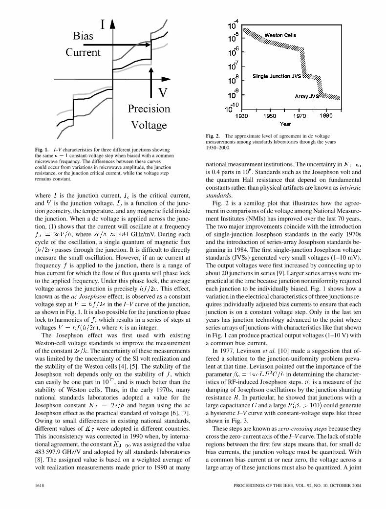
Fig. 1. I–V characteristics for three different junctions showingthe same n = 1 constant-voltage step when biased with a commonmicrowave frequency. The differences between these curvescould occur from variations in microwave amplitude, the junctionresistance, or the junction critical current, while the voltage stepremains constant.
where is the junction current, is the critical current,and is the junction voltage. is a function of the junc-tion geometry, the temperature, and any magnetic field insidethe junction. When a dc voltage is applied across the junc-tion, (1) shows that the current will oscillate at a frequency
, where GHz/mV. During eachcycle of the oscillation, a single quantum of magnetic flux
passes through the junction. It is difficult to directlymeasure the small oscillation. However, if an ac current atfrequency is applied to the junction, there is a range ofbias current for which the flow of flux quanta will phase lockto the applied frequency. Under this phase lock, the averagevoltage across the junction is precisely . This effect,known as the ac Josephson effect, is observed as a constantvoltage step at in the I–V curve of the junction,as shown in Fig. 1. It is also possible for the junction to phaselock to harmonics of , which results in a series of steps atvoltages , where is an integer.
The Josephson effect was first used with existingWeston-cell voltage standards to improve the measurementof the constant . The uncertainty of these measurementswas limited by the uncertainty of the SI volt realization andthe stability of the Weston cells [4], [5]. The stability of theJosephson volt depends only on the stability of , whichcan easily be one part in 10 , and is much better than thestability of Weston cells. Thus, in the early 1970s, manynational standards laboratories adopted a value for theJosephson constant and began using the acJosephson effect as the practical standard of voltage [6], [7].Owing to small differences in existing national standards,different values of were adopted in different countries.This inconsistency was corrected in 1990 when, by interna-tional agreement, the constant was assigned the value483 597.9 GHz/V and adopted by all standards laboratories[8]. The assigned value is based on a weighted average ofvolt realization measurements made prior to 1990 at many
Fig. 2. The approximate level of agreement in dc voltagemeasurements among standards laboratories through the years1930–2000.
national measurement institutions. The uncertainty inis 0.4 parts in 10 . Standards such as the Josephson volt andthe quantum Hall resistance that depend on fundamentalconstants rather than physical artifacts are known as intrinsicstandards.
Fig. 2 is a semilog plot that illustrates how the agree-ment in comparisons of dc voltage among National Measure-ment Institutes (NMIs) has improved over the last 70 years.The two major improvements coincide with the introductionof single-junction Josephson standards in the early 1970sand the introduction of series-array Josephson standards be-ginning in 1984. The first single-junction Josephson voltagestandards (JVSs) generated very small voltages (1–10 mV).The output voltages were first increased by connecting up toabout 20 junctions in series [9]. Larger series arrays were im-practical at the time because junction nonuniformity requiredeach junction to be individually biased. Fig. 1 shows how avariation in the electrical characteristics of three junctions re-quires individually adjusted bias currents to ensure that eachjunction is on a constant voltage step. Only in the last tenyears has junction technology advanced to the point whereseries arrays of junctions with characteristics like that shownin Fig. 1 can produce practical output voltages (1–10 V) witha common bias current.
In 1977, Levinson et al. [10] made a suggestion that of-fered a solution to the junction-uniformity problem preva-lent at that time. Levinson pointed out the importance of theparameter in determining the character-istics of RF-induced Josephson steps. is a measure of thedamping of Josephson oscillations by the junction shuntingresistance . In particular, he showed that junctions with alarge capacitance and a large could generatea hysteretic I–V curve with constant-voltage steps like thoseshown in Fig. 3.
These steps are known as zero-crossing steps because theycross the zero-current axis of the I–V curve. The lack of stableregions between the first few steps means that, for small dcbias currents, the junction voltage must be quantized. Witha common bias current at or near zero, the voltage across alarge array of these junctions must also be quantized. A joint
1618 PROCEEDINGS OF THE IEEE, VOL. 92, NO. 10, OCTOBER 2004

Fig. 3. I–V curve showing the zero-crossing steps of a highcapacitance underdamped junction (large � ). This curve issymmetric in I and V .
effort in 1984 between the National Bureau of Standards inthe United States and the Physikalisch-Technische Bunde-sanstalt in Germany resolved the problems of junction sta-bility and microwave distribution and created the first largeJosephson array based on Levinson’s idea [11]. Further de-sign improvements and system development produced thefirst practical 1-V Josephson standards in 1985 [12], [13].Advances in superconductive integrated circuit technology,driven largely by the quest for a Josephson-junction com-puter, soon made much larger arrays possible. In 1987, thedesign was extended to a chip with 14 484 junctions that gen-erated about 150 000 quantized voltages spanning the rangefrom 10 to 10 V [14]. By 1989, all of the hardware andsoftware for a complete voltage metrology system was com-mercially available. Today, with installations in more than50 national, industrial, and military standards laboratoriesaround the world, this conventional JVS is the only widelyused application of a large-scale superconducting integratedcircuit.
While zero-crossing steps have been the enablingtechnology for conventional voltage standards, they have twoinherent and undesirable features: it is difficult to quicklyselect specific voltage steps, and noise can induce spon-taneous transitions in the step number . In the followingsections, we shall see that overcoming these disadvantageshas been a major occupation of metrologists over the last15 years. We describe how new junction technologies havebeen developed that are capable of producing uniform junc-tion characteristics for large arrays. This has enabled theprogrammable voltage standard with digitally selectable andstable output voltages, and the pulse-driven voltage standardthat can synthesize arbitrary waveforms with fundamentalaccuracy. In this paper we focus on the essential technologythat was developed for the conventional Josephson standard,and for the newer systems under development. For a moredetailed review of the practical aspects of Josephson stan-dards see Hamilton [15]. A more physics-oriented view ofelectrical metrology and Josephson standards, can be foundin reviews by Niemeyer [16] and Kautz [17], [18].
Fig. 4. Thin-film structure of a superconductor–insulator–superconductor Josephson junction typically used in conventionaldc voltage standards.
II. CONVENTIONAL JOSEPHSON ARRAY DESIGN
Fig. 4 illustrates the basic structure of one junction in alarge series array. The junction is an overlap between twosuperconductive thin films that are separated by a thin oxidebarrier. The junction sits above a ground plane and is sepa-rated from it by a few micrometers of insulation. A dc current
and a microwave current are driven through the junc-tion. The design parameters for the junction are its length ,width , critical-current density (critical current per unitarea), and the microwave drive frequency .
Stable operation requires that four conditions be satisfied.
1) must be small enough that the flux induced throughthe junction area by the microwave magnetic field ismuch less than the flux quantum .
2) Both and must be small enough that the lowestresonant cavity mode of the junction is greater than .
3) To avoid chaotic behavior, the junction plasma fre-quency , which is proportional to , must be lessthan about one-third .
4) To prevent noise-induced quantum step transitions, thejunction’s critical current should be aslarge as possible.
If any of these conditions is violated, the junction voltage islikely to switch randomly among several steps, making mea-surements impossible [17], [18]. Fig. 5 illustrates the regionof stable behavior in the three-dimensional space of , ,and . The margin of stable operation, represented by theshaded volume in Fig. 5, increases with and is ultimatelyset by a tradeoff between stability and the economics of pro-viding a very high frequency microwave source. Most prac-tical standards operate in the range 70–96 GHz.
The I–V curve shown in Fig. 3 shows steps covering therange from about 1 mV to 1 mV and is for a junctiondriven by a nearly optimum amplitude of microwave cur-rent. At lower amplitude the steps cover a smaller range ofvoltage, and at higher amplitude the steps are small and donot cross the zero-current axis. In a large array, every junc-tion must generate a large zero-crossing step and, thus, the
BENZ AND HAMILTON: APPLICATION OF THE JOSEPHSON EFFECT TO VOLTAGE METROLOGY 1619

Fig. 5. Three-dimensional visualization of the region of stablevoltage operation as a function of junction length L, width W ,and critical-current density J .
Fig. 6. (a) Series of Josephson junctions arranged to form amicrostrip transmission line. (b) Electrical circuit of a typical JVS.
microwave power must be adjusted to a value low enoughto accommodate the one junction receiving the largest mi-crowave drive. In order to obtain the largest voltage from thesmallest number of junctions, the circuit design must delivernearly uniform microwave power to many thousands of junc-tions, all of which are connected in series. The solution to thisproblem is a simple extension of Fig. 4 to a series array ofjunctions in a line over a ground plane as shown in Fig. 6(a).The capacitive impedance of these underdamped junctions isso small (approximately 1 m at the drive frequency) rela-tive to the stripline impedance (approximately 3 ) that eachjunction has a very minor effect on the propagation of mi-crowave power in the strip line. This junction stripline canpropagate microwave power through 1000 or more junctionswith relatively low loss [11].
A series/parallel circuit similar to that shown in Fig. 6(b)is used to make the arrays of 15 000 junctions that are re-quired to reach operation at 10 V. A network of low- andhigh-pass filters allows the microwave power to be split intomultiple parallel paths while maintaining a dc path in whichall junctions are connected in series.
A typical integrated-circuit layout for an array of20 208 junctions is shown in Fig. 7. The microwave drivepower is collected from a waveguide by a finline antenna,split 16 ways and injected into 16 microstrip lines, eachcontaining 1263 junctions. Microwave power is applied byinserting the finline end of the chip into a slot parallel to theE-field in a WR-12 waveguide.
III. CONVENTIONAL VOLTAGE STANDARD SYSTEMS
A block diagram of a modern JVS system is shownin Fig. 8. The Josephson-array chip is mounted inside ahigh-permeability magnetic shield at the end of a cryoprobethat makes the transition between a liquid-helium dewar andthe room-temperature environment. Three pairs of thermo-couple-grade copper wires are connected to the array. Onepair supplies bias current, a second pair monitors the arrayvoltage with an oscilloscope, and the third pair delivers thearray voltage to the calibration system. All of the wirespass through multiple levels of RF interference filtering.Microwave power is delivered through an overmoded cir-cular waveguide consisting of a 12-mm-diameter tube withWR-12 launching horns on each end. This waveguide si-multaneously achieves low thermal loss ( 0.5 L of liquidHe per day) and low microwave loss (as low as 0.7 dB/mat 75 GHz). A phase-locked oscillator (PLO) operating ata frequency near 75 GHz provides the microwave power tothe chip. The reference frequency for the PLO is typicallyobtained from a cesium clock or a global positioning system(GPS) receiver.
As discussed previously, the zero-crossing steps of Fig. 3allow a single-bias current while ensuring that every junctionin a large array is on a constant-voltage step. Fig. 9(a) illus-trates a simplified diagram of the bias circuit. In this circuit, acomputer sets the bias voltage with one digital-to-analogconverter (DAC) and uses a second DAC to control the biasimpedance via optically modulated resistors. Fig. 9(b)shows a graphical solution for the stable operating points ofthe array and illustrates how control of both the bias voltageand the bias impedance is used to select a particular quantumvoltage step [19]. The load line plots the range of voltage andcurrent that is defined by the bias supply. The intersections ofthis load line with the I–V curve of the array (vertical lines)are possible stable bias points. Changes to shift the loadline left and right, whereas changes to change its slope.To select a step at a given voltage , the source voltageis set to about and the source impedance is set to about
, where is the step height. This makesthe load line steep enough to intersect only one or two stepsand forces the array to a step at or very near . Applyinga damped oscillation to helps move the array to the stepclosest to . After a step is selected, the source impedance
1620 PROCEEDINGS OF THE IEEE, VOL. 92, NO. 10, OCTOBER 2004

Fig. 7. Layout of a 20 208 junction 10-V Josephson array voltage standard chip.
Fig. 8. Block diagram of a modern conventional voltage standard system.
is smoothly increased on all four bias connections (load linebecomes horizontal) until the array current goes to zero andthe array is effectively disconnected from the bias source.This open-bias condition is the most stable state for the arrayand eliminates the possibility of any errors resulting frombias current flowing through a small series resistance in thearray—an occasional array defect. Computer control of thisthree-step process enables the system to find and stabilizethe array voltage on a particular step within a few seconds.
High-quality Josephson arrays will remain on a selected stepfor many hours.
Fig. 8 illustrates the basic method of measuring an un-known voltage relative to a Josephson voltage by placing theJosephson array and the unknown signals in series opposi-tion across the input terminals of a sensitive digital voltmeter(DVM). Accuracy is improved by reversing the measurementleads and by averaging the DVM measurements for severalminutes. The DVM measurements, reversals, and array step
BENZ AND HAMILTON: APPLICATION OF THE JOSEPHSON EFFECT TO VOLTAGE METROLOGY 1621

Table 1Potential Sources of Error and Uncertainty for a Josephson Standard
Fig. 9. (a) The bias circuit for a Josephson junction array.Light-emitting diodes control the bias resistance R by modulatingphotoconductive resistors (represented by arrows). (b) A graphicalsolution of the operating points for the array.
selection are all controlled by a computer. Systems like thatshown in Fig. 8 are used to calibrate secondary standards,such as Weston cells, Zener references, and precise digitalvoltmeters. The typical uncertainty in measurements of 10-VZener standards is limited by noise in the Zener to about0.01 parts in 10 . The ability to set the Josephson array to awide range of discrete voltages also makes it the most accu-rate tool for measuring the linearity of high-accuracy DVMs.
IV. UNCERTAINTY
While the voltage appearing across the terminals ofa Josephson device is given exactly, in principle, by
, in any real measurement there are a varietyof potential sources of error and uncertainty, as listed inTable 1. In the case of a known error, such as a reference-fre-quency offset or a known leakage resistance, a correctioncan be made. It is the metrologist’s task to assign realisticnumbers to all uncertainties including the uncertainty in thecorrections. Note that only items 1 and 2 in Table 1 dependon the magnitude of the voltage being measured, while allof the other components are about the same regardless of thevoltage. Therefore, the combined effect of items 3–8 can bequantitatively evaluated by making a set of measurementsof a short circuit using exactly the same settings (microwavefrequency and power, bias, etc.) and algorithm as is usedfor any other measurement. The standard error resultingfrom items 3–8 is just the root-mean-square (rms) valueof the set of short-circuit measurements [20]. Additionalexperiments must be performed to estimate frequency andleakage uncertainty. Internationally accepted procedures forcombining uncertainties and establishing confidence inter-vals are the subject of the BIPM’s Guide to the Evaluation ofUncertainty in Measurement. Typically, the total uncertaintyof a Josephson system is a few nanovolts. Since the mostcommon use of these systems is the calibration of Zenerstandards with a noise level of 50–100 nV, the contributionof the Josephson system is negligible.
V. PROGRAMMABLE VOLTAGE STANDARDS
Conventional JVSs based on the zero-crossing steps of se-ries arrays of hysteretic junctions have two important dis-advantages: (1) the step number cannot be quickly set toa desired value and (2) noise may cause spontaneous tran-sitions between steps. The step-transition problem requiresthat the bandwidth of all connections to the chip be severelyrestricted in order to filter out noise. In the case of classicaldc measurements, these are minor inconveniences that canbe easily dealt with in software. However, the step stability,step selection, and bandwidth problems preclude measure-ments such as the rapid automated analysis of analog-to-digital (A/D) and digital-to-analog (D/A) converters and thesynthesis of ac waveforms with a computable rms value. Inorder to address these applications, two new standards havebeen developed, one of which focuses on producing stableprogrammable dc voltages, while the other can produce acvoltages and arbitrary waveforms.
1622 PROCEEDINGS OF THE IEEE, VOL. 92, NO. 10, OCTOBER 2004

VI. STABLE PROGRAMMABLE DC VOLTAGE
For the applications that require stable and programmabledc voltages, a new type of JVS has been developed in whichthe output voltage is defined by dividing aseries array of total junctions into smaller independentlybiased programmable segments and then digitally program-ming the junction step number for the junctions in eachsegment [21]. The key to this new Josephson standard isthe use of low-capacitance damped junctions that are de-signed to be nonhysteretic, that is, the junction voltage is asingle-valued function of the junction current, as in Fig. 1.This is achieved by choosing to have a value less thanone. This, of course, brings us back to the situation in 1980when it was deemed that arrays of such junctions would re-quire individual bias currents to ensure that each junctionwas biased on a constant-voltage step. There are two reasonswhy this is now practical. First, in a number of different tech-nologies [22]–[25], junction fabrication has advanced to thepoint where arrays of many thousands of junctions have vari-ations in critical current and resistance of only a few percent.Second, better microwave design allows very uniform distri-bution of power to very large arrays [26]. These technologicalimprovements allow a design in which each junction is typ-ically biased only to the , or steps,and large voltages are obtained by using very large arrays.The result is a large increase in the operating margin, that is,the range of current over which every junction is biased onthe same constant-voltage step.
The circuit for this new programmable JVS (PJVS) uses anarray of nonhysteretic junctions that is divided into a binarysequence of array segments, as shown in Fig. 10(a), [21]. Themicrowave excitation for each junction is set to equalize theamplitude of the and steps, as shown inFig. 10(b). Each segment of the array can be set to the
, or step by applying a bias current atthe appropriate nodes. The combined total step number forthe whole array can, thus, be set to any integer value between
and , where is the total number of junctions inthe array. For example, to select step 5 we would set
. This would bias the single junctionand the set of four junctions on the step and leave allother junctions on the step.
The rapid settling time and inherent step stability of thePJVS in Fig. 10 make it potentially superior to a conventionalJVS for dc measurements. (We define a dc measurement tobe one in which the transient associated with changing canbe excluded from the measurement.) Such measurements in-clude calibration of dc reference standards and digital volt-meters, and the characterization of A/D and D/A converters.The circuit of Fig. 10 can also generate a staircase approxi-mation to a sine wave by selecting appropriate step numbersin rapid succession. In theory, the resulting waveform hasa computable rms value and might be used to confirm theac–dc difference of a thermal voltage converter and for otherac measurements. In the case of ac measurements, however,the transient waveform during step transitions is included in
Fig. 10. (a) Circuit schematic of a programmable voltage standardbased on a set of binary weighted arrays. (b) I–V curve of a singlejunction with the microwave power set to equalize the amplitude ofthe n = 0 and n = �1 steps.
the rms value and may lead to an unacceptably large uncer-tainty. Work continues to make this approach practical for acsynthesis at frequencies below 1 kHz [27], [28] and for fastreversed dc calibrations [29], [30].
The National Institute of Standards and Technology(NIST) has produced a PJVS system that is based on junc-tions with niobium superconductors and palladium–goldnormal metal barriers [22]. Yield and fabrication have madepossible PJVS chips with over 30 000 junctions [26]. Pho-tographs of one of these chips are shown in Fig. 11(a) and11(b). These chips can be rapidly programmed to precise dcvoltages between 1.1 and 1.1 V. Custom bias and mea-surement electronics were implemented in order to achievecomplete automation and programmability of the outputvoltage [31]. A second and more important reason for au-tomation is that the voltage steps of nonhysteretic junctions,unlike the zero-crossing steps of the conventional standard,must be occasionally checked to make sure that they areflat in voltage. The precision voltage is compromised ifthe steps are not flat because these arrays are continuouslycurrent biased, and the current flowing through any seriesresistance between the voltage leads will produce an errorvoltage. Nonflat steps are not a concern in the conventionalJVS because no current flows through the array once it issettled on a quantum step.
With full automation to quickly program voltages andto check for step flatness, the PJVS is now a complete,easy-to-use system. NIST PJVS systems are being usedin a number of applications, including primary dc voltagecalibration at NIST, Watt-balance experiments at both NIST[32] and the Swiss Federal Office of Metrology (OFMET)[33], [34], and a metrology triangle experiment at the French
BENZ AND HAMILTON: APPLICATION OF THE JOSEPHSON EFFECT TO VOLTAGE METROLOGY 1623
Fig. 11. (a) Photograph of NIST’s 1 � 1 cm 32 768 junctionprogrammable-array chip. (b) Section of coplanar waveguideshowing the distribution of junctions along the center conductor.
Laboratorie Central des Industries Electriques (LCIE) [35].Both experiments require stable precision voltages with highnoise immunity, which can be provided by the large ( 1 mAcurrent range) voltage steps of the PJVS. Other metrologylaboratories have focused their PJVS development programson applications to higher voltage [36] or operation at highertemperature [37].
VII. AC VOLTAGE AND ARBITRARY WAVEFORMS
Although quite useful in several new applications, binaryprogrammable arrays have not been very successful in thesynthesis of ac waveforms because the undefined voltageduring transitions between steps adds an unacceptable levelof uncertainty. Another approach in which the array is bi-ased with pulses has the potential to solve this problem. Thusfar, we have discussed ways to program the voltage of aJosephson array by changing the step number in the equa-tion . It is clear that the same result mightbe achieved by changing . Unfortunately, in the case of a
Fig. 12. Comparison of the normalized n = 1 step boundaries fora junction driven with a pulse train (black) and a CW (shaded) as afunction of normalized frequency = f=f .
sine-wave excitation, the step amplitudes—that is, the cur-rent range over which the steps are at constant voltage—col-lapse rapidly to zero as the frequency decreases. This meansthat it is practical to control the voltage via the frequency overonly a small range of frequency. However, if the sine-waveexcitation is replaced with a pulse excitation, then the stepamplitude becomes nearly independent of the pulse repe-tition frequency. Driving a Josephson junction with a cur-rent pulse of the proper amplitude and duration will causethe junction to make exactly one perfectly quantized voltagepulse. Fig. 12 shows a calculation of the step currentboundaries for a junction driven with a sine wave (black area)and a pulse train (shaded area) [38], [39]. Note that for a pulsedrive, the step amplitude (range of dc current bias) is large,symmetric around zero, and independent of frequency all theway to zero frequency. This is because the shape of the cur-rent-drive pulse (in amplitude and duration) determines theoperating range of the junctions, and not the spacing betweenpulses, as for a continuous sine-wave (CW) drive. If the pulsepolarity is reversed, then the array can generate both positiveand negative voltages [40].
A programmable voltage source based on this idea con-sists of a single large array of junctions distributedalong a wide-bandwidth transmission line. A pulse train atfrequency propagating down the line generates a time-av-eraged voltage across the ends of the array. Acomplex output waveform can be generated by modulatingthe pulse train with a digital word generator. For example,using a clock frequency of GHz, the10-b pulse sequence createsan output square wave of amplitude of andfrequency of 1 GHz.
Fig. 13 is a block diagram of the process that is used togenerate an accurate sine wave of frequency or any otherperiodic waveform from quantized Josephson pulses [40].The modulator algorithm block is a computer program thatdigitizes an input signal at a sampling frequency .The algorithm is a second-order delta–sigma modulator thatoptimizes the signal-to-quantization-noise ratio over a de-sired frequency band [41]. For a repetitive waveform, thecode generated by the modulator is calculated just once andstored in the circulating memory of a digital code generator.
1624 PROCEEDINGS OF THE IEEE, VOL. 92, NO. 10, OCTOBER 2004

Fig. 13. (a) Block diagram of a delta–sigma DAC based onbipolar pulsed Josephson junctions [40]. S(t) is the desiredwaveform and S (t) is the synthesized output waveform. (b) Srepresents a coarse bipolar bitstream signal applied in parallel withthe microwave ac bias. The frequency f of the microwave bias isset to an odd half-integer multiple of the sampling frequency, e.g.,f = 3f =2, in order to generate bipolar Josephson pulses for thedesired integrated analog output waveform S .
When the digital code generator is clocked at the samplingfrequency, it creates a timed series of bias-current pulses forwhich the low-frequency spectral components approximatethe original signal. The physics of Josephson junctions al-lows these pulses to be quantized to a single-flux quantum,that is, the time integral of their voltage is exactly equal to
mV ps. It has been shownboth theoretically and experimentally that quantizing thepulses leads to a reduction in noise on the order of 60 dB [39],[42]. When the ratio is large, (e.g., 10 ) the in-bandcomponent of the voltage across the array is an almost perfectreproduction of the input signal. With quantized pulses, aknowledge of the digital code, the sampling frequency, andthe number of junctions in the array is sufficient to exactlycompute thespectrumandthe rmsvalueofoutput signal .
The pulse-driven Josephson array has the potential to beboth a dc voltage standard and an ac voltage standard witha bandwidth of 1 MHz or more. The importance of perfectquantization for precision waveform synthesis can be seenin Fig. 14, where a digital code is chosen to synthesize ananalog waveform with no even harmonics, but where the oddharmonics are specifically chosen to decrease by precisely10 dB for each higher odd-harmonic tone. Nonlinearities inthe digital code generator (DCG) cause significant distortionin its output signal and inaccurate voltage reproduction ofthe odd tones as seen in Fig. 14(a). However, this DCGsignal is adequate to drive the Josephson arrays, creatingperfectly quantized Josephson pulses so that the Josephsonarray output gives the desired precision output voltagewaveform, as seen in Fig. 14(b). Similar comparisons ofdistortion for sine waves synthesized by DCG and Josephsonarrays are presented in [39] and [40]. Precision quantizedJosephson output signals are of great interest for calibrationand metrology applications.
Although the above demonstration shows the power ofperfect quantization from Josephson arrays, there remainmany challenges to developing this Josephson arbitrarywaveform synthesizer as a practical ac JVS (ACJVS). The
Fig. 14. Fourier spectra for a synthesized waveform having onlyodd-harmonic tones whose amplitudes are consecutively decreasedby 10 dB. The measured signals were synthesized by: (a) a digitalcode generator and (b) a 3750-junction series array. The Josephsonsynthesized tones show the expected spectrum of the desiredsynthesized waveform, while the DCG has incorrect amplitudesfor the odd tones and significant power at even harmonics due tointernal nonlinearities.
Fig. 15. Spectrum analyzer measurement demonstrating�93 dBclow distortion for the ACJVS with two Josephson arrays generatinga 242-mV (zero-to-peak) sine wave at 3.3 kHz using 8200 junctionsat 10 Gb/s. The spectrum measurement used 100-Hz resolutionbandwidth and 100 averages to reduce noise of the measurement.
NIST effort has focused primarily on increasing the outputvoltage to practical levels [40]–[43]. Recent advances incircuit design and fabrication of superconducting integratedcircuits have enabled demonstration of waveforms with arecord 242-mV peak voltage, as shown in Fig. 15 [44].Waveforms at both 3.3 and 33 kHz were demonstrated at thisvoltage, both having harmonic distortion below 93 dBc(dB below the fundamental). This larger output voltageallows practical metrology measurements for the first time.
BENZ AND HAMILTON: APPLICATION OF THE JOSEPHSON EFFECT TO VOLTAGE METROLOGY 1625

In order for the ACJVS system to truly meet the definitionof an “intrinsic” ac and dc standard, there must be a finiterange for each bias parameter over which the output voltagedoes not measurably change [45]. This “flat spot” in the oper-ating margins needs to be confirmed every time the ACJVSsystem is used for precision measurements and for eachsynthesized output waveform generated by the Josephsonarray. Every bias parameter must have a range over whichthe output voltage does not change at the level of parts in10 . Such a “flat spot” was recently found for the ACJVSusing a thermal transfer standard [44]; however, it was notfound at the full output voltage, in spite of the low harmonicdistortion. This is because a very small 100-dBc distortionor error signal in the ACJVS output at the fundamental (witha relative phase of 0 or 180 ) remains undetected by thespectrum analyzer, but still produces an error in the rmsvoltage of ten parts in 10 . At 193 mV (zero-to-peak) and2.8 kHz, we were able to find a flat spot in the operatingmargins for all eight different drive parameters. Using anac/dc transfer standard we confirmed the ACJVS outputflatness to be better than a part in 10 . This is an importantstep toward developing a complete ac system.
VIII. HIGHER PERFORMANCE WITH LUMPED ARRAYS
One of the development goals for improving Josephsonsystems is to further increase the output voltage for bothprogrammable and ac voltage standards. Present junctionfabrication technologies use distributed arrays, where thejunctions are distributed along a superconducting transmis-sion line over many wavelengths of the microwave-drivefrequency. The performance of these distributed arrays isdegraded by microwave attenuation of the junctions and bystanding waves from reflections. A few years ago, NISTbecame interested in developing nanoscale junctions forlumped arrays [46], [47]. A lumped array is one in which allof the junctions are placed in the transmission line within asmall fraction, say one-eighth to one-quarter, of the wave-length of the highest drive frequency. Our goal is to makea lumped array whose total impedance is equal to the 50-transmission-line impedance and which can generate asmany Josephson pulses as possible. These arrays would bevery efficient because most of the broadband power wouldnot be wasted in a termination resistor, as in distributed-arraycircuits. A single optimized 50- lumped array with 10-mAcritical current and drive frequency matched to the charac-teristic frequency of the junction would be able to producea maximum output voltage of 0.5 V for a single array onthe step and a 1-V output for the step. Theoutput voltage of these lumped arrays would, thus, be fourto eight times that of the distributed arrays. This approachwould increase the output voltage of the ACJVS to 1 V andthe PJVS output voltage to 10 V for ten parallel arrays.
The challenge for lumped arrays is to put the junctionsvery close together. With junction characteristics optimizedfor a drive frequency of 16 GHz, 13 500 series junctions areneeded with a maximum spacing of 120 nm [46], [47]. Thisclose spacing is a significant challenge, since the smallest
Fig. 16. Side view of two series-connected SNS junction stacks.Niobium superconducting layers are shown in black. The junctionbarriers are solid gray. The insulating silicon dioxide dielectricis shown as hashed lines.
Fig. 17. Cross-sectional TEM image of a five-layerNb/(MoSi /Nb) film [50]. Each of the MoSi barriers is 23 nmthick and the thickness of the Nb middle electrode is 20 nm. Theimage shows that the MoSi deposits uniformly on the niobium,even when the niobium is as thin as 20 nm. (Image by JohnBonevich-MSEL, NIST, 2002.)
SNS arrays fabricated using our PdAu-barrier processhave junction spacing of 7 m. Nanometer control of thebarrier thickness, typically 20–30 nm, is essential becausejunction electrical characteristics depend exponentially onbarrier thickness. Lumped-array junctions will, thus, requirenanometer-scale dimensions and control to achieve suffi-cient uniformity.
The most successful approach to creating lumped arrayshas been to place the junctions in vertical stacks, as shownin Fig. 16. The stacked junctions have multiple barriersdeposited alternately with superconducting layers. Adjacentstacks are interconnected with superconducting base andwiring electrodes to create the series arrays. The NationalInstitute of Advanced Industrial Science and Technology(AIST) in Japan demonstrated the first stacked-junctionarrays for programmable standards in 2002 using niobiumnitride superconductors and titanium nitride normal-metalbarriers [48]. In order to accomplish this task at NIST we areinvestigating normal-metal barriers that can be dry-etchedin-situ with the Nb superconductor [49]–[51]. Our mostpromising barrier material to date is MoSi . A transmissionelectron micrograph of two barriers separated by a 20-nm Nbmiddle electrode is shown in Fig. 17. Using MoSi barriers
1626 PROCEEDINGS OF THE IEEE, VOL. 92, NO. 10, OCTOBER 2004

Fig. 18. I–V characteristics without (gray) and with (black) 9-GHzmicrowave bias for a 1000-stack series array of 10-JJ stacks [52].
we can make uniform constant-voltage steps with super-conducting middle electrodes (the Nb between the MoSibarriers in the stacks) as thin as 5 nm [50]. Furthermore,we have shown that the superconducting order parameter(and, thus, the junction electrical characteristics) remainsunaffected, provided the superconducting electrodes are atleast 20 nm thick. This corresponds to a junction spacingof only 40 nm, which is well below the 120-nm maximumspacing for lumped arrays.
Another significant result for Nb–MoSi stacks is the firstdemonstration of operating margins for ac voltage–wave-form synthesis. Precision audio sine waves at 2.5 kHz with73-mV peak voltage were produced when a 2000-junctiondouble-stack array was biased with an 18.5-GHz microwavesignal and a 3-Mb-long digital code clocked at 7.4 Gb/s. Themeasured fast Fourier transform of this waveform showedharmonic distortion lower than 92 dB below the fundamental( 92 dBc), consistent with our best results from circuitswith PdAu-barrier junctions.
The above results show that Nb–MoSi stacks are verypromising for the next generation of voltage standards.However, cooling the stacks and fabrication of tall stacks areissues that are still being addressed. For example, we havefound that the maximum current through a stacked array islimited by the conductivity between the stack and substrate[51]. Fabricating tall stacks with nearly vertical walls inthis multilayer structure is another significant challenge.However, improvements in our etch process have recentlyallowed Hadacek to demonstrate flat constant voltage stepsin an array of ten-junction stacks [52], as shown in Fig. 18.The uniformity of the 10 000 total junctions in the array issufficient to allow a flat step over a current rangegreater than 1 mA (see inset). This range, although suf-ficient, is significantly lower than the expected 4.5-mArange, because the 7 mm-long 1000-stack array is twicethe quarter-wavelength of the 9-GHz drive frequency andis, therefore, not lumped. Nevertheless, this is the firstten-junction stacked array to produce constant-voltage stepsand is an important milestone. However, taller stacks andshorter arrays are needed to achieve the goal of a 50- arraythat acts as a lumped element at its characteristic frequency(16–20 GHz).
IX. SUMMARY
The accuracy and stability of JVSs far surpass thoseof Zener and electrochemical voltage-standard devices.The generated voltage can be adjusted to any value in therange 10 V. The voltage is independent of environmentaland material characteristics because it is derived directlyfrom a fundamental constant, the ratio of the electroncharge to Planck’s constant. International agreement ona defined value for this constant ensures uniformity andreproducibility near 1 part in 10 in the approximately 60Josephson standards located throughout the world. Newlydeveloped programmable Josephson standards act likeDACs with 12 or more bits of resolution and 30 b of absoluteaccuracy. They are being used for fast dc measurementsand metrology experiments that demand great accuracyand noise immunity. The Josephson arbitrary waveformsynthesizer is being developed as a next-generation standardvoltage source with a bandwidth from dc to 1 MHz or more.Its design places great demands on fabrication technology,microwave design, and thermal engineering. Feasibilityexperiments at voltages up to 0.25 V confirm its potentialas a broadband voltage source. New approaches includingstacked junctions and lumped arrays hold the key to thepractical realization of this ultimate standard for voltagemetrology.
ACKNOWLEDGMENT
The authors would like to thank C. Burroughs,P. Dresselhaus, Y. Chong, N. Hadacek, and H. Yamamori(the present members of the quantum voltage project) formaking possible many of these past and current results. Theauthors would also like to thank R. Kautz for many helpfulconversations over many years.
REFERENCES
[1] B. D. Josephson, “Possible new effects in superconducting tun-neling,” Phys. Lett., vol. 1, pp. 251–253, 1962.
[2] S. Shapiro, “Josephson currents in superconducting tunneling, theeffect of microwaves and other observations,” Phys. Rev. Lett., vol.11, pp. 80–82, 1963.
[3] B. N. Taylor, Ed., The International System of Units (SI). Wash-ington, DC: U.S. General Printing Office, 1991, NBS Special Publ.330.
[4] W. H. Parker, D. N. Langenberg, A. Denenstein, and B. N. Taylor,“Determination of e/h using macroscopic phase coherence in super-conductors,” Phys. Rev., vol. 177, p. 639, 1969.
[5] T. F. Finnegan, A. Denenstein, and D. N. Langenberg, “ac-Josephson-Effect Determination of e/h: A standard of electrochem-ical potential based on macroscopic quantum phase coherence insuper conductors,” Phys. Rev. B, Condens. Matter, vol. 4, p. 1487,1971.
[6] B. N. Taylor, W. H. Parker, D. N. Langenberg, and A. Denenstein,“On the use of the AC Josephson effect to maintain standards ofelectromotive force,” Metrologia, vol. 3, p. 89, 1967.
[7] B. F. Field, T. F. Finnegan, and J. Toots, “Volt maintenance at NBSvia 2e/h: A new definition of the NBS volt,” Metrologia, vol. 9, pp.155–166, 1973.
[8] T. J. Quinn, “News from the BIPM,” Metrologia, vol. 26, pp. 69–74,1989.
BENZ AND HAMILTON: APPLICATION OF THE JOSEPHSON EFFECT TO VOLTAGE METROLOGY 1627
[9] T. Endo, M. Koyanagi, and A. Nakamura, “High-accuracy Josephsonpotentiometer,” IEEE Trans. Instrum. Meas., vol. IM-32, pp.267–271, Mar. 1983.
[10] M. T. Levinsen, R. Y. Chiao, M. J. Feldman, and B. A. Tucker, “Aninverse ac Josephson effect voltage standard,” Appl. Phys. Lett., vol.31, p. 776, 1977.
[11] J. Niemeyer, J. H. Hinken, and R. L. Kautz, “Microwave-inducedconstant-voltage steps at one volt from a series array of Josephsonjunctions,” Appl. Phys. Lett., vol. 45, pp. 478–480, 1984.
[12] C. A. Hamilton, R. L. Kautz, R. L. Steiner, and F. L. Lloyd, “A prac-tical Josephson voltage standard at 1 volt,” IEEE Electron DeviceLett., vol. EDL-6, p. 623, Dec. 1985.
[13] J. Niemeyer, L. Grimm, W. Meier, J. H. Hinken, and E. Vollmer,“Stable Josephson reference voltages between 0.1 and 1.3 V forhigh-precision voltage standards,” Appl. Phys. Lett., vol. 47, p. 1222,1985.
[14] F. L. Lloyd, C. A. Hamilton, J. A. Beall, D. Go, R. H. Ono, and R. E.Harris, “A Josephson array voltage standard at 10 V,” IEEE ElectronDevice Lett., vol. 8, pp. 449–450, Oct. 1987.
[15] C. A. Hamilton, “Josephson voltage standards,” Rev. Sci. Instrum.,vol. 71, pp. 3611–3623, Oct. 2000.
[16] B. Seeber, Ed., Handbook of Applied Superconductivity. Philadel-phia, PA: Inst. of Physics, 1998, vol. 2, p. 1813.
[17] R. L. Kautz, “Design and operation of series-array Josephson voltagestandards,” in Metrology at the Frontiers of Physics and Technology,L. Grovini and T. J. Quinn, Eds. Amsterdam, The Netherlands:North-Holland, 1992, p. 259.
[18] R. L. Kautz, “Noise, chaos, and the Josephson voltage standard,”Rep. Prog. Phys., vol. 59, no. 8, pp. 935–992, Aug 1996.
[19] C. A. Hamilton, R. L. Kautz, F. L. Lloyd, R. L. Steiner, and B. F.Fields, “The NBS Josephson array voltage standard,” IEEE Trans.Instrum. Meas., vol. IM-36, pp. 258–261, June 1987.
[20] C. A. Hamilton and Y. H. Tang, “Evaluating the uncertainty ofJosephson voltage standards,” Metrologia, vol. 36, pp. 53–58, 1999.
[21] C. A. Hamilton, C. J. Burroughs, and R. L. Kautz, “Josephson D/Aconverter with fundamental accuracy,” IEEE Trans. Instrum. Meas.,vol. 44, pp. 223–225, Apr. 1995.
[22] S. P. Benz, “Superconductor-normal-superconductor junctions forprogrammable voltage standards,” Appl. Phys. Lett., vol. 67, pp.2714–2716, Oct. 1995.
[23] H. Sachse, R. Pöpel, T. Weimann, F. Müller, G. Hein, and J.Niemeyer, “Properties of PdAu barriers of SNS junctions for pro-grammable voltage standards,” in Applied Superconductivity 1997:Proc. EUCAS 1997, 3rd Eur. Conf. Applied Superconductivity, Inst.Phys. Conf. Series No. 158, 1997, pp. 555–558.
[24] H. Schulze, R. Behr, F. Müller, and J. Niemeyer,“Nb/Al/AlOx/AlOx/Al/Nb Josephson junctions for pro-grammable voltage standards,” Appl. Phys. Lett., vol. 73, pp.996–998, Aug. 17, 1998.
[25] H. Yamamori, M. Itoh, H. Sasaki, A. Shoji, S. P. Benz, and P.D. Dresselhaus, “All-NbN digital-to-analog converters for a pro-grammable voltage standard,” Supercond. Sci. Technol., vol. 14, pp.1048–1051, Nov. 2001.
[26] S. P. Benz, C. A. Hamilton, C. J. Burroughs, T. E. Harvey, and L.A. Christian, “Stable 1 volt programmable voltage standard,” Appl.Phys. Lett., vol. 71, pp. 1866–1868, Sept. 1997.
[27] P. Helistö, J. Nissilä, K. Ojasalo, J. S. Penttilä, and H. Seppä, “ACvoltage standard based on a programmable SIS array,” IEEE Trans.Instrum. Meas., vol. 52, pp. 533–537, Apr. 2003.
[28] P. Kleinschmidt, P. D. Patel, J. M. Williams, and T. J. B. M. Janssen,“Investigation of binary Josephson arrays for arbitrary waveformsynthesis,” IEE Proc.—Sci., Meas. Tech., vol. 149, pp. 313–319,Nov. 2002.
[29] C. J. Burroughs, S. P. Benz, T. E. Harvey, and H. Sasaki, “1 voltJosephson fast reversed dc source,” in Conf. Dig. Conf. PrecisionElectromagnetic Measurements (CPEM 2000), pp. 341–342.
[30] T. Funck, R. Behr, and M. Klonz, “Fast reversed DC measurementson thermal converters using a SINIS Josephson junction array,” IEEETrans. Instrum. Meas., vol. 50, pp. 322–325, Apr. 2001.
[31] C. J. Burroughs, S. P. Benz, C. A. Hamilton, and T. E. Harvey, “Pro-grammable 1 V DC voltage standard,” IEEE Trans. Instrum. Meas.,vol. 48, pp. 279–281, Apr. 1999.
[32] R. L. Steiner, D. B. Newell, and E. R. Williams, “A result from theNIST watt balance and an analysis of uncertainties,” IEEE Trans.Instrum. Meas., vol. 48, pp. 205–208, Apr. 1999.
[33] B. Jeanneret, A. Rüfenacht, and C. J. Burroughs, “High precisioncomparison between SNS and SIS Josephson voltage standards,”IEEE Trans. Instrum. Meas., vol. 50, pp. 188–191, Apr. 2001.
[34] W. Beer, A. L. Eichenberger, B. Jeanneret, B. Jeckelmann, A. R.Pourzand, P. Richard, and J. P. Schwarz, “Status of the METASwatt balance experiment,” IEEE Trans. Instrum. Meas., vol. 52, pp.626–630, Apr. 2003.
[35] G. Geneves and F. Piquemal, “Vers une loi d’ohm quantique: le tri-angle metrologique,” Cong. Int. Métrol.-Nîmes, pp. 352–357, Oct.1995.
[36] J. Kohlmann, H. Schulze, R. Behr, F. Müller, and J. Niemeyer, “10V SINIS Josephson junction series arrays for programmable voltagestandards,” IEEE Trans. Instrum. Meas., vol. 50, pp. 192–194, Apr.2001.
[37] A. Shoji, H. Yamamori, M. Ishizaki, S. P. Benz, and P. D. Dressel-haus, “Operation of a NbN-based programmable Josephson voltagestandard chip with a compact refrigeration system,” IEEE Trans.Appl. Superconduct., vol. 13, pp. 919–921, June 2003.
[38] S. P. Benz and C. A. Hamilton, “A pulse-driven programmableJosephson voltage standard,” Appl. Phys. Lett., vol. 68, pp.3171–3173, May 1996.
[39] S. P. Benz, C. A. Hamilton, C. J. Burroughs, T. E. Harvey, L.A. Christian, and J. X. Przybysz, “Pulse-driven Josephson dig-ital/analog converter,” IEEE Trans. Appl. Superconduct., vol. 8, pp.42–47, June 1998.
[40] S. P. Benz, C. A. Hamilton, C. J. Burroughs, and T. E. Harvey, “ACand dc bipolar voltage source using quantized pulses,” IEEE Trans.Instrum. Meas., vol. 48, pp. 266–269, Apr. 1999.
[41] J. C. Candy, “An overview of basic concepts,” in Delta–SigmaData Converters: Theory, Design, and Simulation, S. R. Nor-sworthy, R. Schreier, and G. C. Temes, Eds. Piscataway, NJ:IEEE, 1997.
[42] S. P. Benz, C. J. Burroughs, and P. D. Dresselhaus, “Low harmonicdistortion in a Josephson arbitrary waveform synthesizer,” Appl.Phys. Lett., vol. 77, no. 7, pp. 1014–1016, Aug. 2000.
[43] , “AC coupling technique for Josephson waveform syn-thesis,” IEEE Trans. Appl. Supercond., vol. 11, pp. 612–616,June 2001.
[44] C. J. Burroughs, R. J. Webber, P. D. Dresselhaus, and S. P. Benz,“Operating margin measurements for an AC Josephson voltage stan-dard,” presented at the Session 7e: DC Voltage, Nat. Conf. StandardsLaboratories (NCSL), Tampa Bay, FL, 2003.
[45] C. J. Burroughs, S. P. Benz, and P. D. Dresselhaus, “AC Josephsonvoltage standard error measurements and analysis,” IEEE Trans. In-strum. Meas., vol. 52, pp. 542–544, Apr. 2003.
[46] R. H. Ono and S. P. Benz, “Optimum characteristics of high tem-perature Josephson junctions for “lumped” array applications,”in Extended Abstracts 7th Int. Superconductive Electronics Conf.(ISEC’99), pp. 301–303.
[47] S. P. Benz, P. D. Dresselhaus, and C. J. Burroughs, “Nanotechnologyfor next generation Josephson voltage standards,” IEEE Trans. In-strum. Meas., vol. 50, pp. 1513–1518, Dec. 2001.
[48] H. Yamamori, M. Ishizaki, M. Itoh, and A. Shoji,“NbN/TiN/NbN/TiN/NbN double-barrier junction arraysfor programmable voltage standards,” Appl. Phys. Lett., vol. 80,pp. 1415–1417, Feb. 2002.
[49] P. D. Dresselhaus, Y. Chong, J. H. Plantenberg, and S. P. Benz,“Stacked SNS Josephson junction arrays for quantum voltagestandards,” IEEE Trans. Appl. Superconduct., vol. 13, pp. 930–933,June 2003.
[50] Y. Chong, P. D. Dresselhaus, S. P. Benz, and J. E. Bonevich, “Ef-fects of interlayer electrode thickness in Nb(MoSi /Nb) stackedJosephson junctions,” Appl. Phys. Lett., vol. 82, pp. 2467–2469,Apr. 14, 2003.
[51] Y. Chong, P. D. Dresselhaus, and S. P. Benz, “Thermal trans-port in stacked superconductor-normal metal-superconductorJosephson junctions,” Appl. Phys. Lett., vol. 83, pp. 1794–1796,Sept. 1, 2003.
[52] N. Hadacek, private communication, Sept. 2003.
1628 PROCEEDINGS OF THE IEEE, VOL. 92, NO. 10, OCTOBER 2004

Samuel P. Benz (Senior Member, IEEE) wasborn in Dubuque, IA, on December 4, 1962. Hereceived the B.A. degree in physics and mathe-matics (summa cum laude) from Luther College,Decorah, IA, in 1985 and the M.A. and Ph.D.degrees in physics from Harvard University,Cambridge, MA, in 1987 and 1990, respectively.
In 1990, he began working at the NationalInstitute of Standards and Technology as aNational Institute of Standards and Technology(NIST)/National Research Council (NRC) Post-
doctoral Fellow and joined the permanent staff in January 1992. He hasbeen Project Leader of the Quantum Voltage Project at NIST, Boulder,CO, since 1999. He has authored 92 publications and three patents in thefield of superconducting electronics. He has worked on a broad range oftopics within the field of superconducting electronics, including Josephsonjunction array oscillators, single flux quantum logic, ac and dc Josephsonvoltage standards, and Josephson waveform synthesis.
Dr. Benz is a Member of Phi Beta Kappa and Sigma Pi Sigma. He wasawarded an R. J. McElroy fellowship (1985–1988).
Clark A. Hamilton (Fellow, IEEE) was born inRochester, NY, on April 22, 1944. He received theB.S. degree in electrical engineering from UnionCollege, Schenectady, NY, in 1966, and the M.S.and Ph.D. degrees in electrical engineering fromthe University of Rochester in 1968 and 1971,respectively.
He joined the National Institute of Standardsand Technology (NIST, formerly the NationalBureau of Standards) Boulder, CO, in 1971 andbecame a NIST Fellow in 1987. Most of his
career at NIST has focused on Josephson devices and voltage standards.In 1999, he retired from NIST to start his own company, VMetrix LLC,Boulder, which specializes in system design, consulting, and trainingrelated to Josephson voltage standards. He has authored 80 publicationsand holds three patents.
Dr. Hamilton shared IR100 awards for his work on infrared detectors(1976) and Josephson array voltage standards (1987), and he has receivedtwo U.S. Department of Commerce Gold Medals for his work on super-conducting integrated circuits using Josephson devices (1984 and 1989).He received the 1995 IEEE Electrotechnology Transfer Award.
BENZ AND HAMILTON: APPLICATION OF THE JOSEPHSON EFFECT TO VOLTAGE METROLOGY 1629


![A Practical Josephson Voltage Standard at One Volt · A Practical Josephson Voltage Standard at One Volt This paper [1] is considered the seminal, definitive paper describing the](https://img.pdfslide.net/doc/110x75/5e3a4c96938cf41b8122d18b/a-practical-josephson-voltage-standard-at-one-volt-a-practical-josephson-voltage.jpg)