Embed Size (px)
Citation preview

Topics• Target Markets• Signal Path/Device Examples• DSP Interface Example• Power Supply Considerations• Thermal Overview• PCB Layout• Key Components – Critical Parameters• Putting it all together
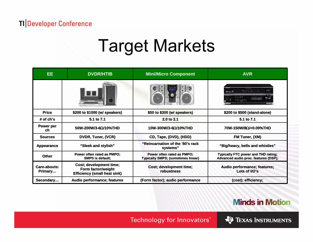
Target Markets
(cost); efficiency; (Form factor); audio performanceAudio performance; featuresSecondary…
Audio performance; features;Lots of I/O’s
Cost; development time;robustness
Cost; development time;Form factor/weight
Efficiency (small heat sink)Care-abouts:
Primary…
“Big/heavy, bells and whistles”“Reincarnation of the ’80’s rack systems”“Sleek and stylish”Appearance
Typically FTC power and THD rating;Advanced audio proc. features (DSP);
Power often rated as PMPO;Typically SMPS; (sometimes linear)
Power often rated as PMPO;SMPS is default; Other
FM Tuner, (XM)CD, Tape, (DVD), (HDD)DVDR, Tuner, (VCR)Sources
10W-300W/3-6Ω/10%THD
2.0 to 2.1
$50 to $300 (w/ speakers)
Mini/Micro Component
50W-200W/3-6Ω/10%THD
5.1 to 7.1
$200 to $1000 (w/ speakers)
DVDR/HTIB
70W-150W/8Ω/<0.09%THDPower per ch
5.1 to 7.1
AVR
# of ch’s
$200 to $500 (stand-alone)Price
EE

Conventional Signal PathDAC needed
Analog processingComplex & long analog signal path:
Sound degradation!!!
High Analog Gain: Sensitive to noise & Hum pick upSNR at speakers is much lower than theoretical DAC spec
Filter& buffer
AnalogSound Control
DIGITALDOMAIN
ANALOGDOMAIN
DAC 14dB 30dB
VOLCTL.
PRE-AMP.
PWRAMP.
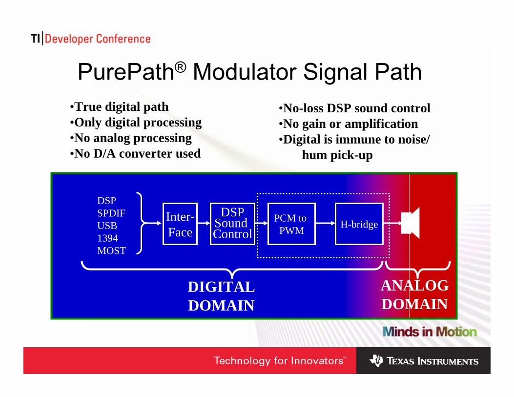
PurePath® Modulator Signal Path•True digital path•Only digital processing•No analog processing•No D/A converter used
•No-loss DSP sound control•No gain or amplification •Digital is immune to noise/
hum pick-up
Inter-Face
DSPSound Control
PCM to PWM H-bridge
DSPSPDIFUSB1394MOST
DIGITALDOMAIN
ANALOGDOMAIN
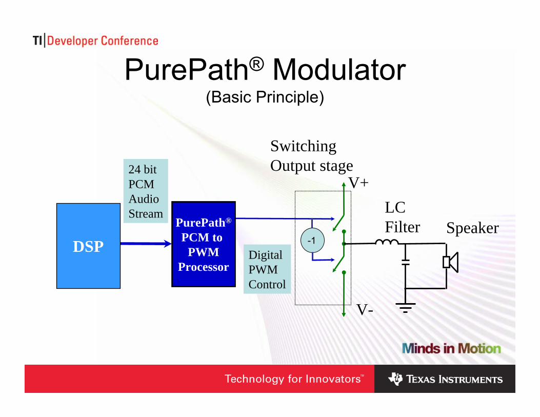
PurePath® Modulator(Basic Principle)
PurePath®
PCM to PWM
ProcessorDSP
LCFilter Speaker
SwitchingOutput stage24 bit
PCMAudioStream
DigitalPWMControl
V+
V-
-1
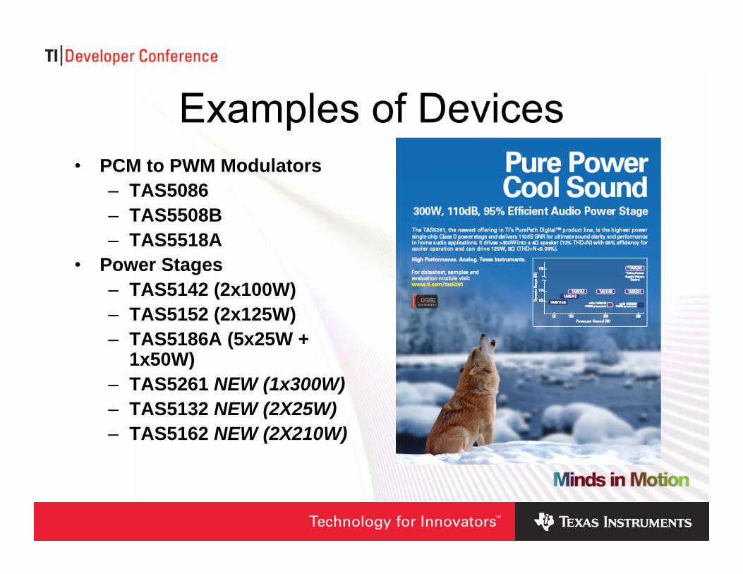
Examples of Devices• PCM to PWM Modulators
– TAS5086– TAS5508B– TAS5518A
• Power Stages– TAS5142 (2x100W)– TAS5152 (2x125W)– TAS5186A (5x25W +
1x50W)– TAS5261 NEW (1x300W)– TAS5132 NEW (2X25W)– TAS5162 NEW (2X210W)

DSP Interface Example

DSP/Amplifier Interconnect
Interface Port to Amplifiers

DSP Connection to Modulator
From DSP
PWM
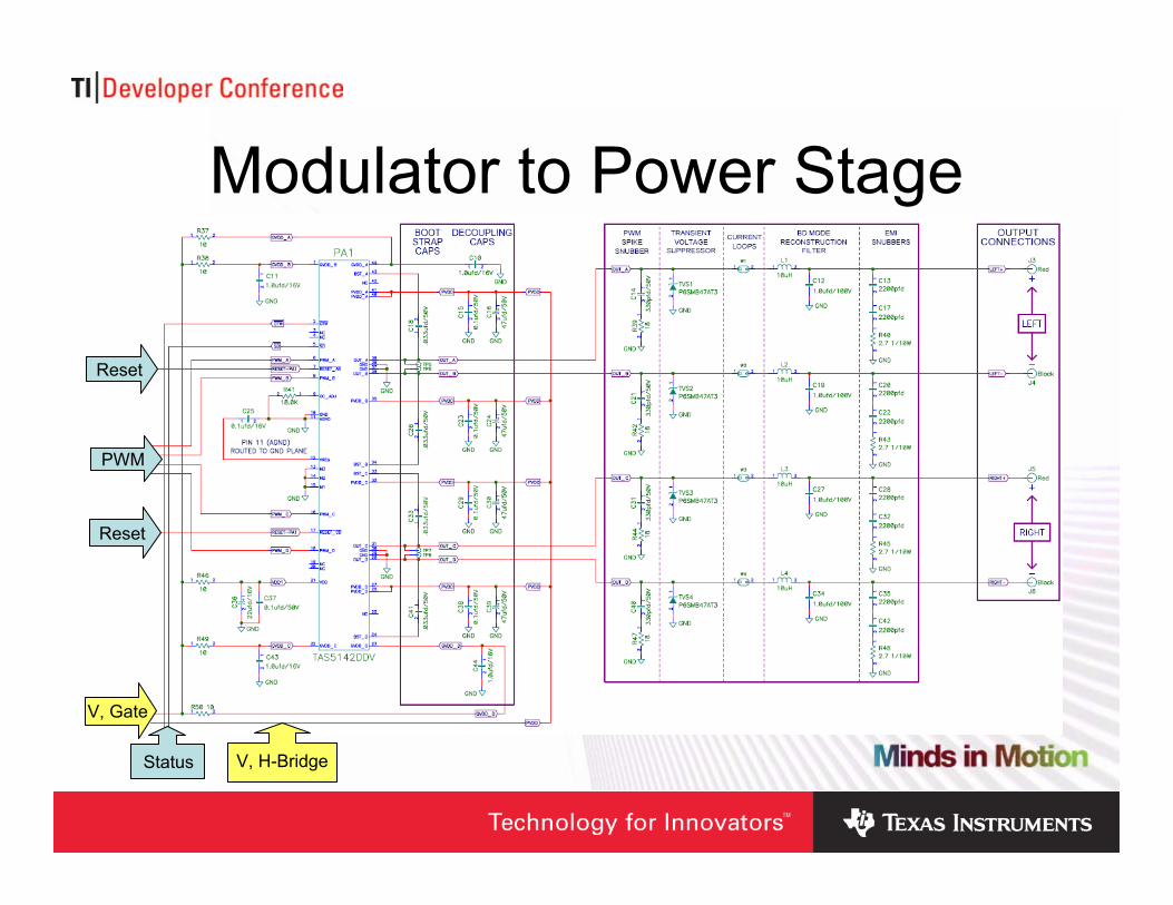
Modulator to Power Stage
PWM
Reset
Reset
V, H-Bridge
V, Gate
Status
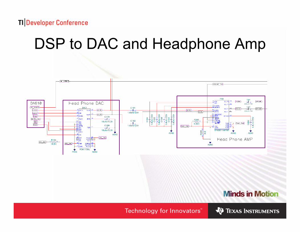
DSP to DAC and Headphone Amp

Power Supply Considerations

• Using following equation:– Voltage needed for an application can be calculated as:
Voltage Requirement
( )( )
MR
PRRRV LOAD
MAXINDUCTORDSonLOAD
PSU
⎟⎠⎞⎜
⎝⎛ ⋅⋅+⋅+
=
22
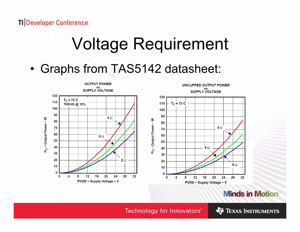
Voltage Requirement• Graphs from TAS5142 datasheet:
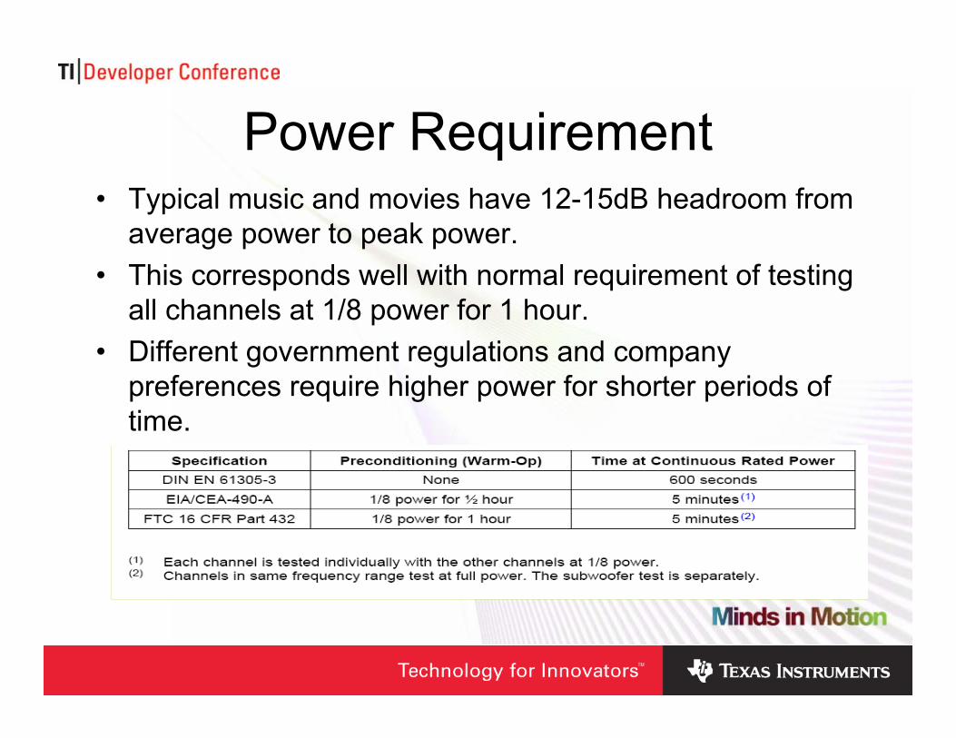
Power Requirement• Typical music and movies have 12-15dB headroom from
average power to peak power.• This corresponds well with normal requirement of testing
all channels at 1/8 power for 1 hour.• Different government regulations and company
preferences require higher power for shorter periods of time.

Power Supply Rejection Ratio• PSRR is well known for class AB amplifiers.
• Normal definitions of PSRR also apply for Class D amplifiers using feedback.
• PurePath® digital amplifiers do not use feedback; PSRR term is slightly different:– Vout(t) = Vpsu(t) x d(t)
• Conventional mains transformer supply will have 100Hz/120Hz ripple.
• Common Switch Mode Power Supplies (SMPS) switch in the 100KHz to 200KHz range; therefore, their ripple is out of the audio band and they are regulated.
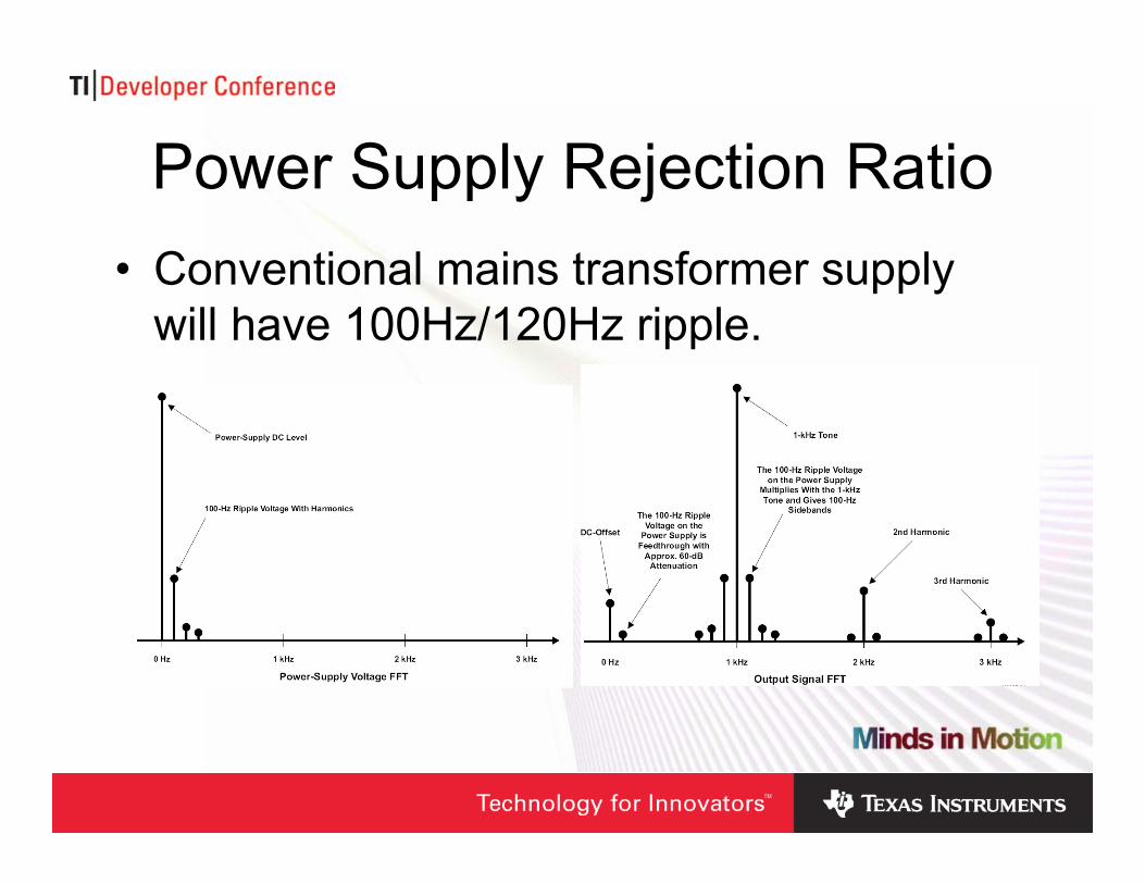
Power Supply Rejection Ratio• Conventional mains transformer supply
will have 100Hz/120Hz ripple.

Power Supply Rejection Ratio• A switch mode power supply will not have
ripple within the audio band.
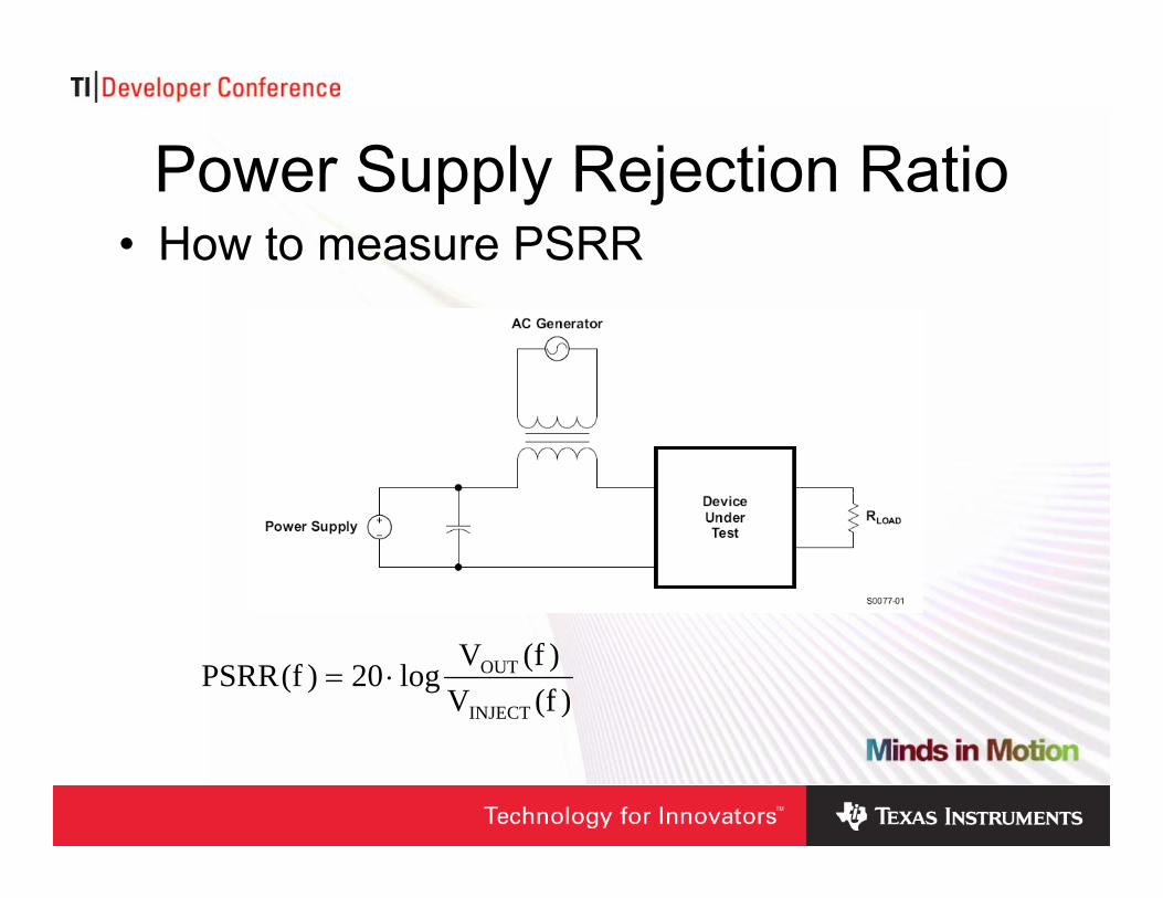
Power Supply Rejection Ratio• How to measure PSRR
)f(V)f(V
log20)f(PSRRINJECT
OUT⋅=

Power Supply Rejection Ratio
PSRR measurement for TAS5086-5142V6EVM
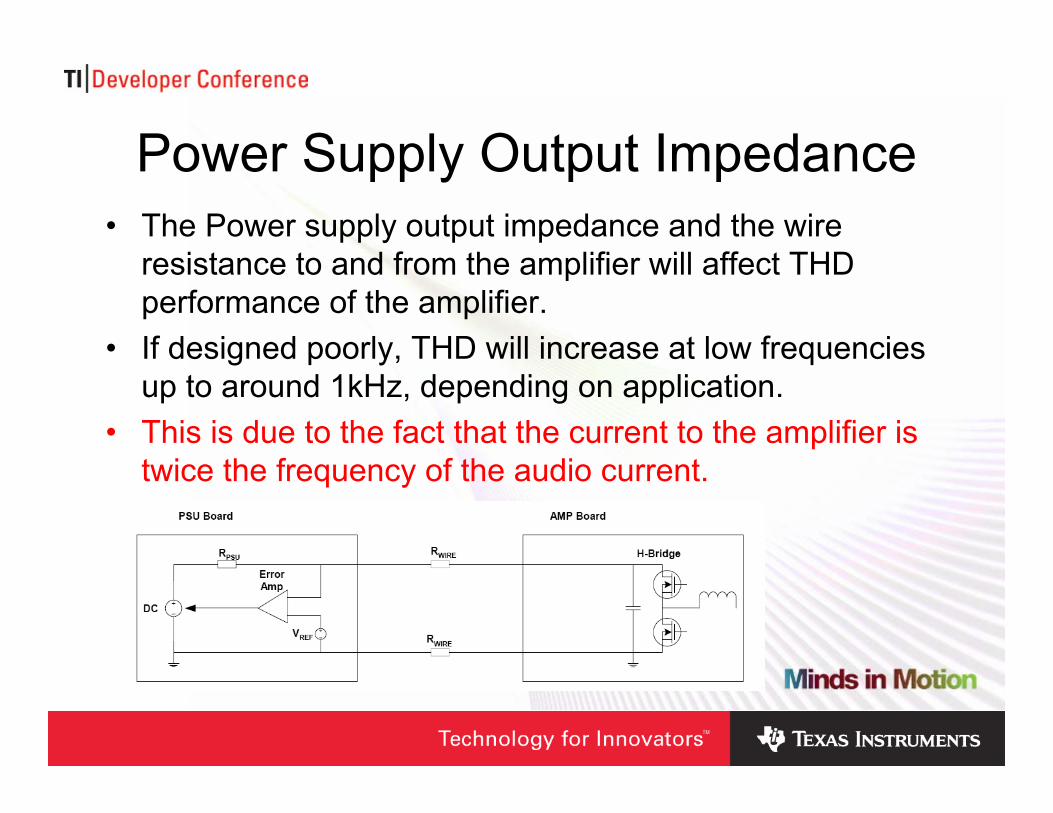
Power Supply Output Impedance• The Power supply output impedance and the wire
resistance to and from the amplifier will affect THD performance of the amplifier.
• If designed poorly, THD will increase at low frequencies up to around 1kHz, depending on application.
• This is due to the fact that the current to the amplifier is twice the frequency of the audio current.

Power Supply Output Impedance
Blue Line – High power supply Output ImpedanceGreen Line – Correct power supply Ouput Impedance
More Info• Power Supply Recommendations for DVD Receivers, TI
Literature No. SLEA027• Power Supply Recommendations for A/V Receivers, TI
Literature SLEA028• PSRR for PurePath Digital Audio Amplifiers, TI Literature
SLEA049

Thermal Overview
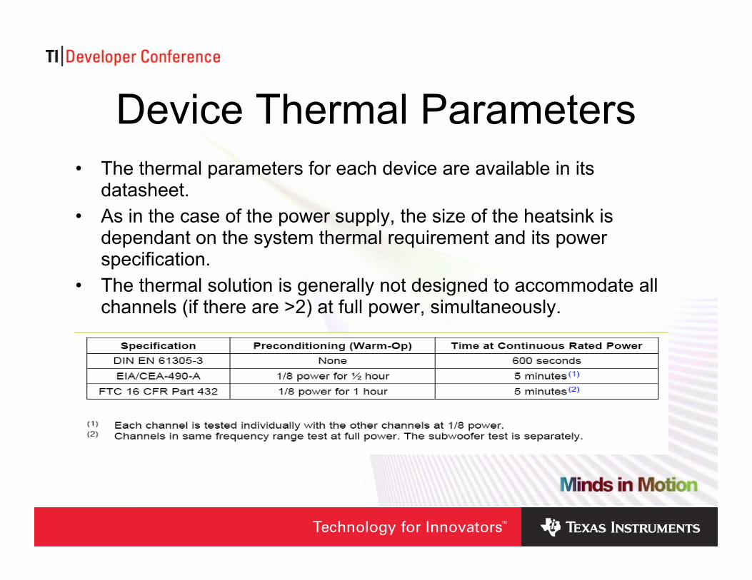
Device Thermal Parameters• The thermal parameters for each device are available in its
datasheet.• As in the case of the power supply, the size of the heatsink is
dependant on the system thermal requirement and its power specification.
• The thermal solution is generally not designed to accommodate all channels (if there are >2) at full power, simultaneously.
Heatsink Size• In many cases a heatsink of 2.5°/W to 4.5°C is
appropriate.– There are many variables such as airflow and test
temperature to be considered.• TI EVMs are delivered with a good thermal solution.
– It may be necessary to change the size or geometry to meet space constraints or other system factors.

PCB Layout- Do’s and Don’ts
PCB Layout and EMI• PCB layout, Audio Performance and EMI are linked closely together.
• Generally EMI is concerned with reducing EMI sources and removing antennas.
• Circuit contains high currents at high frequencies.
• Care must be taken to prevent unwanted ringing and spikes.
• Current loops with high currents and high frequencies act as EMIsources and must be kept as small as possible.
• Small signal level CMOS inputs can pick up noise and must therefore be kept away from EMI sources.
Ground Plane
Ground Plane The forgotten return path• Every signal has a return current.• Routing of the return path is just as important as signal
current.• The best/only solution is the use of a ground plane.• Ground plane is an unbroken Cu-PCB layer only used for
ground signal.• Optimum path for return currents then becomes embedded
in the design.• Note that optimum return path is not necessarily the
shortest path for high frequency currents.

Routing of Sensitive Tracks• Decoupling capacitors must be placed close to the device.
Goal - .050” of PCB track length in decoupling path.
• All Power tracks must be designed with care to get good audio and EMI performance.
• PWM tracks must go as directly as possible from TAS5086/TAS5508 to TAS5142 and other power stages. The tracks must not interleave the PCB.
• MCLK track must be as short as possible and must always be accompanied by ground.

Implementation of TAS5142
• PWM output voltage goes from 0V to 32V within 5ns.• Ripple current in inductors is 2A at 384kHz in idle.
Implementation of TAS5142
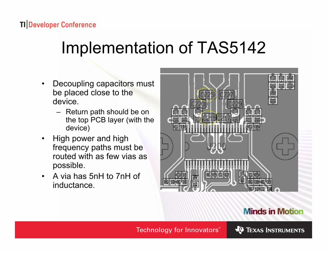
• Decoupling capacitors must be placed close to the device.– Return path should be on
the top PCB layer (with the device)
• High power and high frequency paths must be routed with as few vias as possible.
• A via has 5nH to 7nH of inductance.

PCB Ground Domains• PCB must be divided into a high power zone and a low power zone.
High powerelectronics
Low powerand sensitiveelectronics
This does not mean split the plane! (or you may develop a “Contentious Plane”)
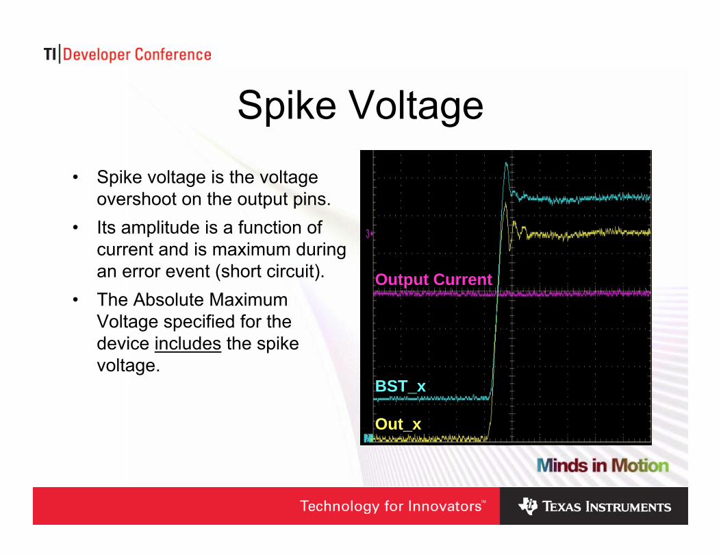
Spike Voltage• Spike voltage is the voltage
overshoot on the output pins.• Its amplitude is a function of
current and is maximum during an error event (short circuit).
• The Absolute Maximum Voltage specified for the device includes the spike voltage.
Out_x
BST_x
Output Current
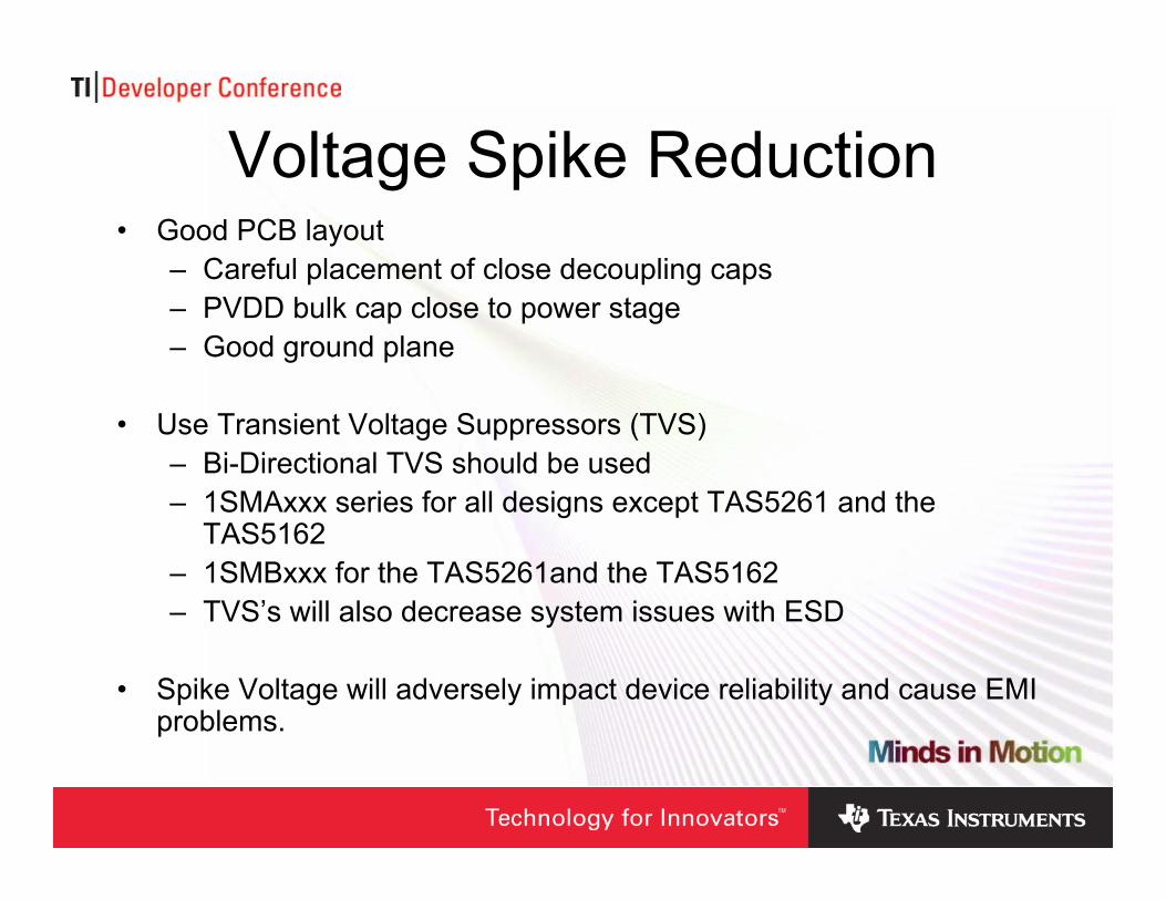
Voltage Spike Reduction• Good PCB layout
– Careful placement of close decoupling caps– PVDD bulk cap close to power stage– Good ground plane
• Use Transient Voltage Suppressors (TVS)– Bi-Directional TVS should be used– 1SMAxxx series for all designs except TAS5261 and the
TAS5162– 1SMBxxx for the TAS5261and the TAS5162– TVS’s will also decrease system issues with ESD
• Spike Voltage will adversely impact device reliability and cause EMI problems.

Key Components –and their Critical Parameters
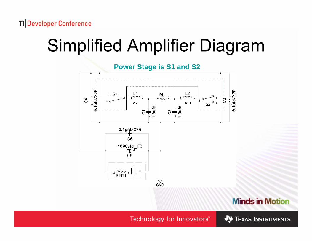
Simplified Amplifier DiagramPower Stage is S1 and S2
Amplifier Component Considerations• Choice of components sets the
audio performance.• MOSFET Switches (taken care
of by the power stage)• PWM Filter Capacitor (use a
film capacitor)– Stability with voltage– Ripple Current
• Inductor (use TI recommended)– Series resistance (dc), skin
effect (ac)– Parallel resistance
(hysteresis loss)– Parallel capacitance– Saturation in core material
• Decoupling capacitor (use X7R)– Series resistance– Series inductance
• Bulk Capacitor (Use low ESR)– ESR– ESL– Ripple Current
• PSU– Output impedance– Current limitation– Current Slew-rate– Surge Capability
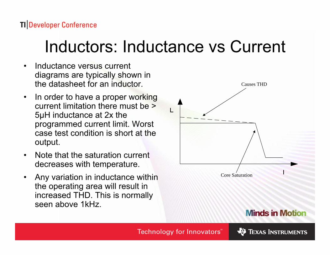
Inductors: Inductance vs Current• Inductance versus current
diagrams are typically shown in the datasheet for an inductor.
• In order to have a proper working current limitation there must be > 5μH inductance at 2x the programmed current limit. Worst case test condition is short at the output.
• Note that the saturation current decreases with temperature.
• Any variation in inductance within the operating area will result in increased THD. This is normally seen above 1kHz.
Core Saturation
Causes THD
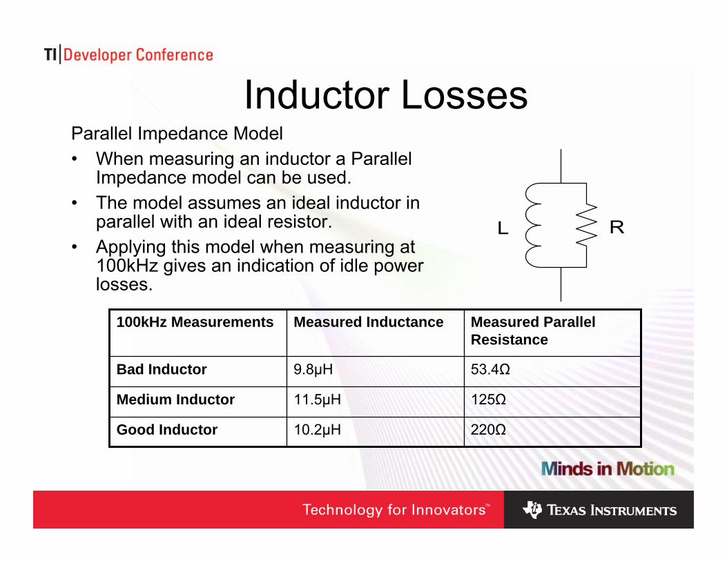
Inductor LossesParallel Impedance Model• When measuring an inductor a Parallel
Impedance model can be used.• The model assumes an ideal inductor in
parallel with an ideal resistor.• Applying this model when measuring at
100kHz gives an indication of idle power losses.
220Ω10.2μHGood Inductor
125Ω11.5μHMedium Inductor
53.4Ω9.8μHBad Inductor
Measured Parallel Resistance
Measured Inductance100kHz Measurements
More Info• Magnetics Design Handbook, MAG100A, (Texas
Instruments)– Available from TI Website
PWM Filter Capacitor Considerations• Capacitor Types
– Metal Film Capacitors, linear over applied voltage
– Ceramic X7R, change value over applied voltage resulting in increase THD
• SMD – Leaded
– SMD capacitors, especially ceramic capacitors, change physical size over applied voltage.
– This will result in audible noise and mechanical stress of the part and its soldering.

Putting It All Together
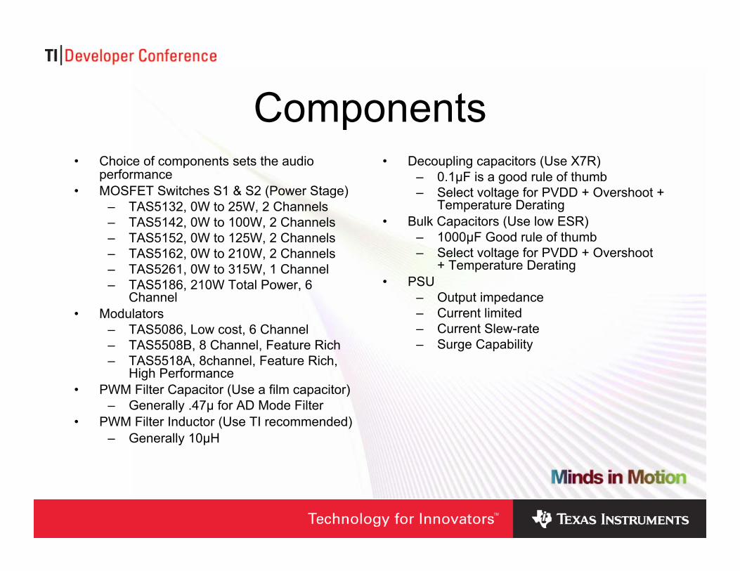
Components• Choice of components sets the audio
performance• MOSFET Switches S1 & S2 (Power Stage)
– TAS5132, 0W to 25W, 2 Channels– TAS5142, 0W to 100W, 2 Channels– TAS5152, 0W to 125W, 2 Channels– TAS5162, 0W to 210W, 2 Channels– TAS5261, 0W to 315W, 1 Channel– TAS5186, 210W Total Power, 6
Channel• Modulators
– TAS5086, Low cost, 6 Channel– TAS5508B, 8 Channel, Feature Rich– TAS5518A, 8channel, Feature Rich,
High Performance• PWM Filter Capacitor (Use a film capacitor)
– Generally .47μ for AD Mode Filter• PWM Filter Inductor (Use TI recommended)
– Generally 10μH
• Decoupling capacitors (Use X7R)– 0.1μF is a good rule of thumb– Select voltage for PVDD + Overshoot +
Temperature Derating• Bulk Capacitors (Use low ESR)
– 1000μF Good rule of thumb– Select voltage for PVDD + Overshoot
+ Temperature Derating• PSU
– Output impedance– Current limited– Current Slew-rate– Surge Capability
Getting Started• TI has a complete library of EVMs and
reference designs @ www.ti.com -- follow the design carefully .
• Contact your local TI FSE for assistance.