Embed Size (px)
Citation preview
FPRF MIMO Transceiver IC With Integrated Microcontroller
LMS7002M
Document version: 2.2.r0 Last modified: 26/09/2014
SUMMARY FEATURES
Field Programmable Radio Frequency (FPRF) chip
Dual transceiver ideal for MIMO
User programmable on the fly
Continuous coverage of the 100 kHz - 3.8 GHz RF frequency range
Digital interface to baseband with on chip integrated 12 bit D/A and A/D converters
Programmable RF modulation bandwidth up to 120 MHz using analog interface
Programmable RF modulation bandwidth up to 56 MHz using digital interface
Supports both TDD and full duplex FDD
LimeLight™ digital IQ interface – JEDEC JESD207 TDD and FDD compliant
Transceiver Signal Processor block employs advanced techniques for enhanced performance
Single chip supports 2x2 MIMO. Multiple chips can be used to implement higher order MIMO
On-chip RF calibration circuitry
Fully differential baseband signals, analog IQ
Few external components
Low voltage operation, 1.25, 1.4 and 1.8V. Integrated LDOs to run on a single 1.8V supply voltage
On chip integrated microcontroller for simplified calibration, tuning and control
Integrated clock PLL for flexible clock generation and distribution
User definable analog and digital filters for customised filtering
RF and base band Received Signal Strength Indicator (RSSI)
261 pin aQFN 11.5x11.5 mm package
Power down option
Serial port interface
Low power consumption, typical 880mW in full 2x2 MIMO mode (550mW in SISO mode) using external LDOs
Multiple bypass modes for greater flexibility
APPLICATIONS
Broad band wireless communications
GSM, CDMA2000, TD-SCDMA, WCDMA/HSPA, LTE
IEEE® xxx.xxx radios
WiFi operating in the Whitespace frequencies
Software Defined Radio (SDR)
Cognitive Radio
Unmanned Aerial Vehicle (UAV)
Other Whitespace applications
RX BB
TX BB
LPF
TX BB
LPF
RXLNAL
RXLNAH
RXLNAW
RXINL
RXINH
RXINW
RXLNAL
RXLNAH
RXLNAW
RXINL
RXINH
RXINW
RX LO
Chain
RX
Synthesizer
RXMIX
RXMIX
RXTIA
RXTIA
TX BB
LPF
TX BB
LPF
TX LO
Chain
TX
Synthesizer
TXPAD
TXPAD
RXLPF
RXLPF
TXLPF
TXLPF
ADC
ADC
ADC
ADC
DAC
DAC
DAC
DAC
TXPAD
TXPAD
Power
Det.
Power
Det.
Switch
Switch
RX BB
Power
Det.
Power
Det.
Switch
Switch
Connects to LNA
output in RF Loop Back
mode
TXOUT1
TXOUT2
TXOUT1
TXOUT2
RXPGA
RXPGA
Tra
nsce
ive
r S
ign
al P
roce
sso
r (T
SP
)
Lim
eL
igh
tTM
Dig
ita
l IQ
In
terf
ace
, P
ort
2
TXMIX
TXMIX
Lim
eL
igh
tTM
Dig
ita
l IQ
In
terf
ace
, P
ort
1
DLB
TXINI, TXINQ
TXINI, TXINQ
RXOUTI, RXOUTQ
RXOUTI, RXOUTQ
RXOUTSW
RXOUTSW
RF
RSSI
SPIMicro
ControllerClock PLLRF
RSSI
Connects to LNA
output in RF Loop Back
mode
Connects to LNA
output in RF Loop Back
mode
Connects to LNA
output in RF Loop Back
mode
Figure 1: Functional block diagram
2 LMS7002M
LMS7002M – FPRF MIMO Transceiver IC
GENERAL DESCRIPTION
LMS7002M is a fully integrated, multi-band, multi-standard RF transceiver that is highly programmable. It combines Low Noise Amplifiers (RXLNA), TX Power Amplifier Divers (TXPAD) receiver/transmitter (RX/TX) mixers, RX/TX filters, synthesizers, RX gain control, TX power control, the analog-to-digital and digital-to-analog convertors (ADC/DACs) and has been designed to require very few external components. The top level architecture of LMS7002M transceiver is shown in Figure 1. The chip contains two transmit and two receive chains for achieving a Multiple In Multiple Out (MIMO) platform. Both transmitters share one PLL and both receivers share another. Transmit and receive chains are all implemented as zero Intermediate Frequency (zero IF or ZIF) architectures providing up to 112MHz RF modulation bandwidths (equivalent to 56MHz baseband IQ bandwidth). For the purpose of simplifying this document, the explanation for the functionality and performance of the chip is based on one transmit and one receive circuitry, given that the other two work in exact the same manner. On the transmit side, In-phase and Quadrature IQ DAC data samples, from the base band processor, are provided to the LMS7002M via the LimeLight™ digital IQ interface. LimeLight™ implements the JESD207 standard IQ interface protocol as well as de facto IQ multiplexed standard. JESD207 is Double Data Rate (DDR) by definition. In IQ multiplexed mode LimeLight™ also supports Single Data Rate (SDR). The IQ samples are then pre-processed by the digital Transceiver Signal Processor (TSP) for minimum analog / RF distortion and applied to the on chip transmit DACs. The DACs generate analog IQ signals which are provided for further processing to the analog/RF section. Transmit low pass filters (TXLPF) remove the images generated by zero hold effect of the DACs, as well as the DAC out-of-band noise. The analog IQ signals are then mixed with the transmit PLL (TXPLL) output to produce a modulated RF signal. This RF signal is then amplified by one of two separate / selectable power amplifier drivers and two open-drain differential outputs are provided as RF output for each MIMO path.
Transmitter gain control range of 70 dB is provided by integrated digital TSP and TXPAD. Both stages have 1 dB gain step control. The LMS7002M provides an RF loop back option which enables the TX RF signal to be fed back into the baseband for calibration and test purposes. The RF loop back signal is amplified by the loopback amplifier in order to increase the dynamic range of the loop. There are two additional loop back options implemented, one is an analog base band (BB) loop back and another is a digital loop back (DLB) as shown in Figure 1. The analog loop back is intended for testing while the DLB can be used to verify the LMS7002M connectivity to base band, FPGA, DSP or any other digital circuitry. On the receive side, three separate inputs are provided each with a dedicated LNA optimised for narrow or wide band operation. Each port RF signal is first amplified by a programmable low noise amplifier (RXLNA). The RF signal is then mixed with the receive PLL (RXPLL) output to directly down convert to baseband. AGC steps can be implemented by a BB transimpedance amplifier (RXTIA) prior to the programmable bandwidth low pass channel select filters (RXLPF). The received IQ signal is further amplified by a programmable gain amplifier RXPGA. DC offset is applied at the input of RXTIA to prevent saturation and to preserve the receive ADC’s dynamic range. The resulting analog receive IQ signals are converted into the digital domain with on-chip receive ADCs. Following the ADCs, the signal conditioning is performed by the digital Transceiver Signal Processor (TSP) and the resulting signals are then provided to the BB via the LimeLight™ digital IQ interface. The analog receive signals can also be provided off chip at RXOUTI and RXOUTQ pins by closing the RXOUT switch. In this case it is possible to power down the on chip ADCs/TSP and use external parts which can be very useful for more resource demanding applications or where higher signal resolution is required. A similar option is also available on the TX side where the analog signal can be processed by external components. The on chip DACs/TSP can be powered down and analog inputs can be provided at TXINI and TXINQ pins.
Parameter Min. Typ. Max. Unit Condition/Comment
Operating Temperature Range -40 25 85 °C
Storage Temperature Range -65 25 150 °C
Operating Frequency Range 30 0.1
3800 3800
MHz Extended by TSP NCOs
Baseband Bandwidth 56 120 MHz
Frequency Resolution 24.8 Hz Using 52 MHz PLL reference clock
Analog Supply Voltage, High (VDDAH) 1.71 1.8 1.89 V Used for TXPAD
Analog Supply Voltage, Medium (VDDAM)
1.33 1.4 1.47 V Generated using integrated low-dropout regulators (LDOs)
Analog Supply Voltage, Low (VDDAL) 1.2 1.25 1.3 V Generated using integrated LDOs
Digital Supply Voltage 1.1 1.2 1.3 V Generated using integrated LDOs
TX Supply Current 350 mA At -7 dBm output power, 2x2 MIMO, including the DACs and TSP
RX Supply Current 420 mA For 2x2 MIMO, including the ADCs and TSP
Digital Peripheral (IO) Supply Voltage 2.5 2.7 3.6 V
Maximum RF Output Power 0 dBm Continuous Wave
TX Output Maximum RF Power (CW) 10 dBm
PLL Reference Clock 10 52 MHz
Interpolation/Decimation digital filters stop band suppression
108 dB
Table 1: General specifications
3 LMS7002M
LMS7002M – FPRF MIMO Transceiver IC
Parameter Min. Typ. Max. Unit Condition/Comment
RF channel frequency range 30 0.1
3800 3800
MHz Extended by TSP NCOs
Transmit Analog Input Impedance 400 Ohms Differential, programmable
Transmit Load Impedance at the output pins
40 Ohms Differential, for maximum OIP3
Transmit Differential I and Q Input Current
625 uA
Differential Common mode
Transmit Gain Control Range 70 dB TSP and TXVGA2
Transmit Gain Control Step 1 dB
TX Local Oscillator (LO) Leakage -60 dBc Calibrated
RXLNAL Frequency Range 0.1 2000 MHz Narrow band tunable, set by external matching circuit
RXLNAH Frequency Range 0.1 3800 MHz Narrow band tuneable, set by external matching circuit
RXLNAW Frequency Range 0.1 3800 MHz Broad band tuneable, set by external matching circuit
Noise Figure 2.0 2.5 3.5
dB at 0.95GHz at 2GHz at 3.8GHz
2rd Order Input Intercept Point 50 dBm
Total receiver gain ~50 dB or more, Noise Figure <3.5 dB in all bands. Two tone signals out of band.
3rd Order Input Intercept Point 4 dBm
Total receiver gain ~50 dB or more, Noise Figure <3.5 dB in all bands. Two tone signals out of band.
Receive Gain Control Range 70 dB RXLNA, RXTIA, RXPGA, RXTSP combined
Receive Gain Control Step 0.5 1 1.5 dB
Table 2: General RF specifications
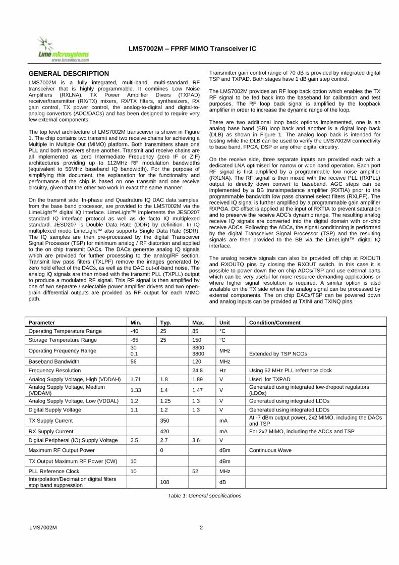
Two transmitter outputs (TXOUT1, TXOUT2) and three receiver inputs (RXINL, RXINH, RXINW) are provided to facilitate multi-band multi-standard operation. The functionality of the LMS7002M is fully controlled by a set of internal registers which can be accessed through a serial port and rapidly reprogrammed on the fly for advanced system architectures. In order to enable full duplex operation, LMS7002M contains two separate synthesisers (TXPLL, RXPLL) both driven from the same reference clock source PLLCLK.
TX GAIN CONTROL
The LMS7002M transmitter has two programmable gain stages, where the TSP provides digital gain control and the TXPAD gives programmable gain of the RF signal.
TXMIX
TXPLL
TXPAD
TXOUT1
TXOUT2
TXINI
TXINQ
Figure 2: TX analog/RF gain control architecture
Parameter Min. Typ. Max. Unit Condition/Comment
Digital TSP Gain Control Range 15 dB In steps of 1 LSB digital gain control
TXPAD Gain Control Range 55 dB
TXPAD Gain Step Size 1 dB for the higher 10 steps
TXPAD Gain Step Size 2 dB for the lower 20 steps
Table 3: TX gain control
LMS7002M – FPRF MIMO Transceiver IC
LMS7002M 4
RX GAIN CONTROL
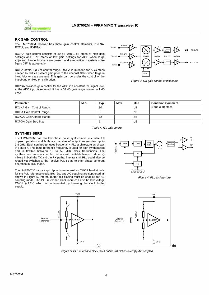
The LMS7002M receiver has three gain control elements, RXLNA, RXTIA, and RXPGA. RXLNA gain control consists of 30 dB with 1 dB steps at high gain settings and 3 dB steps at low gain settings for AGC when large adjacent channel blockers are present and a reduction in system noise figure (NF) is acceptable. RXTIA offers 3 dB of control range. RXTIA is intended for AGC steps needed to reduce system gain prior to the channel filters when large in band blockers are present. This gain can be under the control of the baseband or fixed on calibration. RXPGA provides gain control for the AGC if a constant RX signal level at the ADC input is required. It has a 32 dB gain range control in 1 dB steps.
RXLNAL
RXLNAH
RXLNAW
RXINL
RXINH
RXINW
RXMIX
RXPLL
RXTIA RXLPF RXPGA
RXOUTQ
RXOUTI
Figure 3: RX gain control architecture
Parameter Min. Typ. Max. Unit Condition/Comment
RXLNA Gain Control Range 30 dB 1 and 3 dB steps
RXTIA Gain Control Range 3 dB
RXPGA Gain Control Range 32 dB
RXPGA Gain Step Size 1 dB
Table 4: RX gain control
SYNTHESISERS
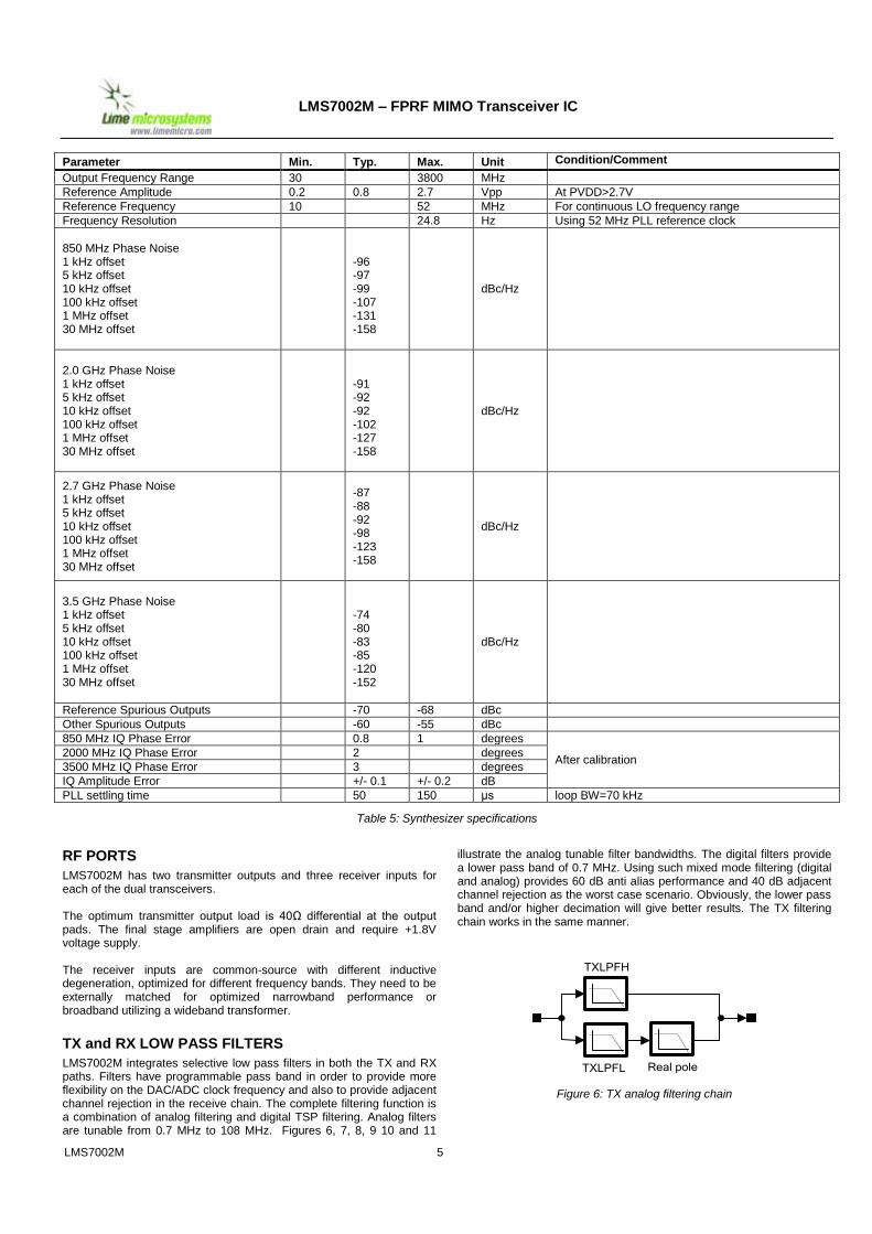
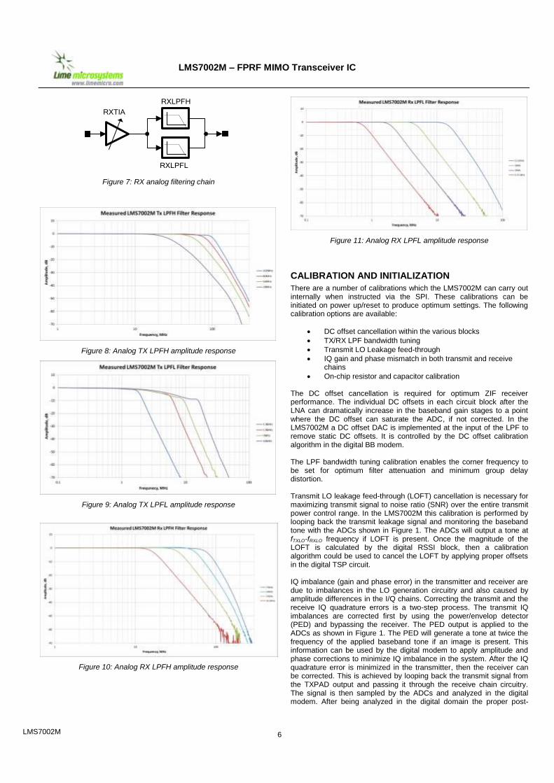
The LMS7002M has two low phase noise synthesizers to enable full duplex operation and both are capable of output frequencies up to 3.8 GHz. Each synthesizer uses fractional-N PLL architecture as shown in Figure 4. The same reference frequency is used for both synthesizers and is flexible between 10 to 52 MHz clock frequencies. The synthesizers produce complex outputs with suitable levels to drive IQ mixers in both the TX and the RX paths. The transmit PLL could also be routed via switches to the receive PLL so as to offer phase coherent operation in TDD mode. The LMS7002M can accept clipped sine as well as CMOS level signals for the PLL reference clock. Both DC and AC coupling are supported as shown in Figure 5. Internal buffer self-biasing must be enabled for AC coupling mode. The PLL reference clock input can also be low voltage CMOS (<1.2V) which is implemented by lowering the clock buffer supply.
PFD CHPLoop
Filter
/N
∆∑
~ Output
Divider
NINT, NFRAC
PL
LC
LK
0º
90º
VCO
Figure 4: PLL architecture
CLKBUF
VSS
VDD
PL
LC
LK
External
Reference
(a)
CLKBUF
VSS
VDD
PL
LC
LK
External
Reference
(b)
Figure 5: PLL reference clock input buffer, (a) DC coupled (b) AC coupled
5 LMS7002M
LMS7002M – FPRF MIMO Transceiver IC
Parameter Min. Typ. Max. Unit Condition/Comment
Output Frequency Range 30 3800 MHz
Reference Amplitude 0.2 0.8 2.7 Vpp At PVDD>2.7V
Reference Frequency 10 52 MHz For continuous LO frequency range
Frequency Resolution 24.8 Hz Using 52 MHz PLL reference clock
850 MHz Phase Noise 1 kHz offset 5 kHz offset 10 kHz offset 100 kHz offset 1 MHz offset 30 MHz offset
-96 -97 -99 -107 -131 -158
dBc/Hz
2.0 GHz Phase Noise 1 kHz offset 5 kHz offset 10 kHz offset 100 kHz offset 1 MHz offset 30 MHz offset
-91 -92 -92 -102 -127 -158
dBc/Hz
2.7 GHz Phase Noise 1 kHz offset 5 kHz offset 10 kHz offset 100 kHz offset 1 MHz offset 30 MHz offset
-87 -88 -92 -98 -123 -158
dBc/Hz
3.5 GHz Phase Noise 1 kHz offset 5 kHz offset 10 kHz offset 100 kHz offset 1 MHz offset 30 MHz offset
-74 -80 -83 -85 -120 -152
dBc/Hz
Reference Spurious Outputs -70 -68 dBc
Other Spurious Outputs -60 -55 dBc
850 MHz IQ Phase Error 0.8 1 degrees
After calibration 2000 MHz IQ Phase Error 2 degrees
3500 MHz IQ Phase Error 3 degrees
IQ Amplitude Error +/- 0.1 +/- 0.2 dB
PLL settling time 50 150 μs loop BW=70 kHz
Table 5: Synthesizer specifications
RF PORTS
LMS7002M has two transmitter outputs and three receiver inputs for each of the dual transceivers. The optimum transmitter output load is 40Ω differential at the output pads. The final stage amplifiers are open drain and require +1.8V voltage supply. The receiver inputs are common-source with different inductive degeneration, optimized for different frequency bands. They need to be externally matched for optimized narrowband performance or broadband utilizing a wideband transformer.
TX and RX LOW PASS FILTERS
LMS7002M integrates selective low pass filters in both the TX and RX paths. Filters have programmable pass band in order to provide more flexibility on the DAC/ADC clock frequency and also to provide adjacent channel rejection in the receive chain. The complete filtering function is a combination of analog filtering and digital TSP filtering. Analog filters are tunable from 0.7 MHz to 108 MHz. Figures 6, 7, 8, 9 10 and 11
illustrate the analog tunable filter bandwidths. The digital filters provide a lower pass band of 0.7 MHz. Using such mixed mode filtering (digital and analog) provides 60 dB anti alias performance and 40 dB adjacent channel rejection as the worst case scenario. Obviously, the lower pass band and/or higher decimation will give better results. The TX filtering chain works in the same manner.
TXLPFH
TXLPFL Real pole
Figure 6: TX analog filtering chain
LMS7002M 6
LMS7002M – FPRF MIMO Transceiver IC
RXTIA
RXLPFH
RXLPFL
Figure 7: RX analog filtering chain
Figure 8: Analog TX LPFH amplitude response
Figure 9: Analog TX LPFL amplitude response
Figure 10: Analog RX LPFH amplitude response
Figure 11: Analog RX LPFL amplitude response
CALIBRATION AND INITIALIZATION
There are a number of calibrations which the LMS7002M can carry out internally when instructed via the SPI. These calibrations can be initiated on power up/reset to produce optimum settings. The following calibration options are available:
DC offset cancellation within the various blocks
TX/RX LPF bandwidth tuning
Transmit LO Leakage feed-through
IQ gain and phase mismatch in both transmit and receive chains
On-chip resistor and capacitor calibration The DC offset cancellation is required for optimum ZIF receiver performance. The individual DC offsets in each circuit block after the LNA can dramatically increase in the baseband gain stages to a point where the DC offset can saturate the ADC, if not corrected. In the LMS7002M a DC offset DAC is implemented at the input of the LPF to remove static DC offsets. It is controlled by the DC offset calibration algorithm in the digital BB modem. The LPF bandwidth tuning calibration enables the corner frequency to be set for optimum filter attenuation and minimum group delay distortion. Transmit LO leakage feed-through (LOFT) cancellation is necessary for maximizing transmit signal to noise ratio (SNR) over the entire transmit power control range. In the LMS7002M this calibration is performed by looping back the transmit leakage signal and monitoring the baseband tone with the ADCs shown in Figure 1. The ADCs will output a tone at fTXLO-fRXLO frequency if LOFT is present. Once the magnitude of the LOFT is calculated by the digital RSSI block, then a calibration algorithm could be used to cancel the LOFT by applying proper offsets in the digital TSP circuit. IQ imbalance (gain and phase error) in the transmitter and receiver are due to imbalances in the LO generation circuitry and also caused by amplitude differences in the I/Q chains. Correcting the transmit and the receive IQ quadrature errors is a two-step process. The transmit IQ imbalances are corrected first by using the power/envelop detector (PED) and bypassing the receiver. The PED output is applied to the ADCs as shown in Figure 1. The PED will generate a tone at twice the frequency of the applied baseband tone if an image is present. This information can be used by the digital modem to apply amplitude and phase corrections to minimize IQ imbalance in the system. After the IQ quadrature error is minimized in the transmitter, then the receiver can be corrected. This is achieved by looping back the transmit signal from the TXPAD output and passing it through the receive chain circuitry. The signal is then sampled by the ADCs and analyzed in the digital modem. After being analyzed in the digital domain the proper post-
LMS7002M 7
LMS7002M – FPRF MIMO Transceiver IC
distortion IQ calibration coefficients are calculated and applied to the receive signals within the TSP block. Please see the “LMS7002M Programming and Calibration Guide” for more details.
TRANSCEIVER SIGNAL PROCESSOR
LMS7002M includes a high digital gate count within the Transceiver Signal Processor (TSP) block. The function of the TSP is to employ advanced digital signal processing techniques to enhance the performance of the analog/RF parts. This results in an improved performance of the overall system and a saving on total current consumption The TSP is placed between the data converters and the LimeLight™ digital IQ interface as shown in Figure 12. Functionally, the RX and TX parts of the TSP are similar, as shown in Figure 13 and 14, respectively.
RXIN1
IQADC
IQADC
RXTSP
RXTSP
TXTSP
TXTSP
Lim
eL
igh
t D
igita
l IQ
In
terf
ace
Ra
dio
Fre
qu
en
cy P
art
of
the
Ch
ip
TSP
IQDAC
IQDAC
RXIN2
RXIN3
RXIN1
RXIN2
RXIN3
TXOUT1
TXOUT2
TXOUT1
TBOUT2
Figure 12: TSP part of the LMS7002M
Decimation
Decimation
IQ Phase
Corr
IQ Gain
Corr
RX DC
Corr
IQ Phase
Corr
IQ Gain
Corr
RX DC
Corr
CMIX
RXNCO
G. P.
FIR 1
G. P.
FIR 1
G. P.
FIR 2
G. P.
FIR 2
RSSI
AG
C
RXI
RXQ RYQ
RYIG. P.
FIR 3
G. P.
FIR 3
Figure 13: Structure of the RXTSP
CMIX
TXNCO
Interpolation
Interpolation
G. P.
FIR 1
G. P.
FIR 2
G. P.
FIR 1
G. P.
FIR 2TXQ
TXIG. P.
FIR 3
G. P.
FIR 3
IQ Phase
Corr
IQ Gain
Corr
TX DC
Corr
IQ Phase
Corr
IQ Gain
Corr
TX DC
Corr
TYI
TYQ
INVSINC
INVSINC
Figure 14: Structure of the TXTSP
In both the TX and RX TSP blocks there are three general purpose finite impulse response (FIR) filters, G.P FIR 1, G.P. FIR 2 and G.P. FIR 3. The filter coefficients are fully programmable and the implementation does not force their impulse response to be symmetrical. On the TX side, one of these filters could be used as a phase equalizer, which is a requirement in some communication standards such as CDMA2000. Another can be used to flatten the amplitude response of the TXLPF while the third FIR could be used to further enhance the channel filtering function of the BB modem. If phase equalization is not required then one filter can be used to minimize group delay variation of the analog TXLPF. Possible applications of the G.P. FIR filters on the RX side are similar. One could be used to minimize group delay variation of the analog RXLPF while another could help to improve RXLPF adjacent channel rejection performance. The interpolation block within the TXTSP takes IQ data from the BB modem and increases the data sample rate. The advantages of having interpolation are as follows. For narrow band systems (GSM/EDGE) or even moderately broad band (WCDMA, CDMA2000) modulation standards, the BB modem does not need to interpolate IQ data to the target system clock. The base band can provide output data at a much lower sample rate saving on power at the digital interface. Having a low data rate interface also simplifies the PCB design. However, the
interpolator block generates data samples at the system clock rate, so the DACs run at a high sampling rate. As the DACs are running at a high frequency, it means that the quantization noise is spread over a wider frequency range which results in a better overall SNR. Also, the image generated by the DAC zero hold effect is further away from the wanted signal hence the specification for the TXLPF can be relaxed. The reason for having decimation in the RXTSP is similar to that of interpolation in TXTSP. The ADCs can run at high frequency, and the specification of the RXLPF used as an anti-alias filter in this case is relaxed, the G.P. FIR improves adjacent channel rejection and the decimation circuit reduces the received data sample rate before sending the data to the BB modem. The two Numerically Controlled Oscillators (NCO) and digital complex mixer (CMIX) in the TXTSP and RXTSP paths enable the LMS7002M to run in low digital IF. Inverse sinc filters (INVSINC) within the TXTSP chain compensate for sinx/x amplitude roll off imposed by the DACs themselves. The Tx DC Corr block is used to cancel residual DC offset of TXLPF. It is also used to cancel TX LO leakage feed-through as mentioned earlier.
LMS7002M 8
LMS7002M – FPRF MIMO Transceiver IC
There are three sources of the DC component at the RX output. These are the residual DC offset of the RXVGAs and RXLPF, RX LO leakage feed-through and second order distortion (IP2). The Rx DC Corr blocks compensate for all of these sources of offset. The block is implemented as a real time tracking loop so any change of the RX DC due to either the signal level change, or due to RX gain change as well as any temperature effect will be tracked and cancelled automatically. The IQ Gain Corr and IQ Phase Corr blocks correct IQ imbalance in both TXTSP and RXTSP in order to minimize the level of unwanted side band (image) component. The last stage in the RXTSP path is a digital implementation of an Adaptive Gain Control (AGC) loop. Assuming that the BB modem does not require 12-bit full scale ADC outputs, the digital AGC block can provide a certain level of automatic gain control before the BB involves RF and IF gain stages. More detailed descriptions of all the various TSP blocks are given in the following sections.
IQ GAIN CORRECTION
This block implements the following equation:
QGQinQout
IGIinIout
_
_
.
Corresponding hardware is given in Figure 15. G_I and G_Q are programmable correction factors which are altered by the BB modem to minimize any unwanted side band component. The BB modem can combine IQ gain correction and digital gain control using the same module by calculating G_I and G_Q in the following way:
digiGcorrQGQG
digiGcorrIGIG
_*___
_*___
,
where G_I_corr and G_Q_corr are IQ gain correction factors and G_digi is the desired digital gain.
G_I
G_Q
Qout
IoutIin
Qin
Figure 15: IQ gain correction implantation
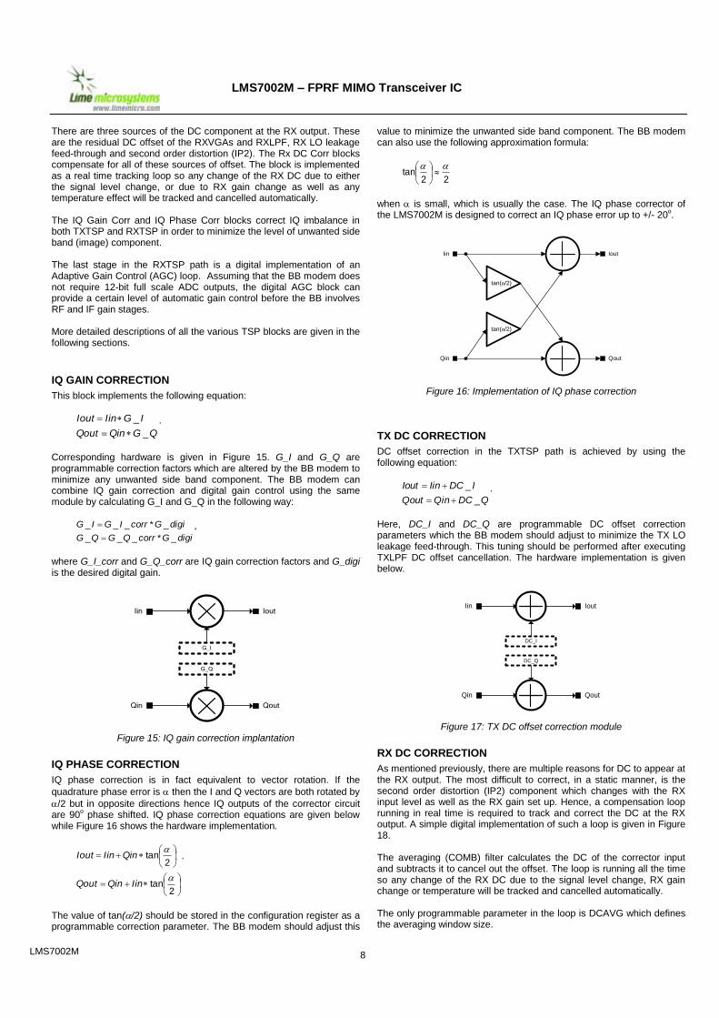
IQ PHASE CORRECTION
IQ phase correction is in fact equivalent to vector rotation. If the
quadrature phase error is then the I and Q vectors are both rotated by
/2 but in opposite directions hence IQ outputs of the corrector circuit are 90
o phase shifted. IQ phase correction equations are given below
while Figure 16 shows the hardware implementation.
2tan
2tan
IinQinQout
QinIinIout .
The value of tan(/2) should be stored in the configuration register as a programmable correction parameter. The BB modem should adjust this
value to minimize the unwanted side band component. The BB modem can also use the following approximation formula:
22tan
when is small, which is usually the case. The IQ phase corrector of the LMS7002M is designed to correct an IQ phase error up to +/- 20
o.
tan(α/2)
tan(α/2)
Qout
IoutIin
Qin
Figure 16: Implementation of IQ phase correction
TX DC CORRECTION
DC offset correction in the TXTSP path is achieved by using the following equation:
QDCQinQout
IDCIinIout
_
_
.
Here, DC_I and DC_Q are programmable DC offset correction parameters which the BB modem should adjust to minimize the TX LO leakage feed-through. This tuning should be performed after executing TXLPF DC offset cancellation. The hardware implementation is given below.
DC_I
DC_Q
Iin
Qin Qout
Iout
Figure 17: TX DC offset correction module
RX DC CORRECTION
As mentioned previously, there are multiple reasons for DC to appear at the RX output. The most difficult to correct, in a static manner, is the second order distortion (IP2) component which changes with the RX input level as well as the RX gain set up. Hence, a compensation loop running in real time is required to track and correct the DC at the RX output. A simple digital implementation of such a loop is given in Figure 18. The averaging (COMB) filter calculates the DC of the corrector input and subtracts it to cancel out the offset. The loop is running all the time so any change of the RX DC due to the signal level change, RX gain change or temperature will be tracked and cancelled automatically. The only programmable parameter in the loop is DCAVG which defines the averaging window size.
LMS7002M 9
LMS7002M – FPRF MIMO Transceiver IC
-
Iin
Qin Qout
Iout
DCAVGC
OM
BC
OM
B
-
Figure 18: RX DC offset correction module
INVERSE SINC FILTER
The inverse sinc filter compensates for sinx/x amplitude roll off imposed by the DAC. The filter is designed to compensate from DC to 0.35fs where fs is the DAC sampling frequency. Impulse and amplitude responses are shown in Figure 19 and Figure 20.a respectively. Figure 20.b plots the equivalent DAC amplitude response with the inverse sinc function compensation applied. The in band (0 - 0.35fs ) amplitude ripple is less than +/- 0.04 dB.
h( 0) = 0.0101318 = h( 4) h( 1) = -0.0616455 = h( 3) h( 2) = 0.855469
Figure 19: INVSINC impulse response
-4
-3.5
-3
-2.5
-2
-1.5
-1
-0.5
0
0 0.05 0.1 0.15 0.2 0.25 0.3 0.35 0.4 0.45 0.5
Mag
nit
ud
e [
dB
]
Frequency [f/fs]
(a)
(b)
Figure 20: INVSINC (a) and equivalent DAC (b) amplitude response
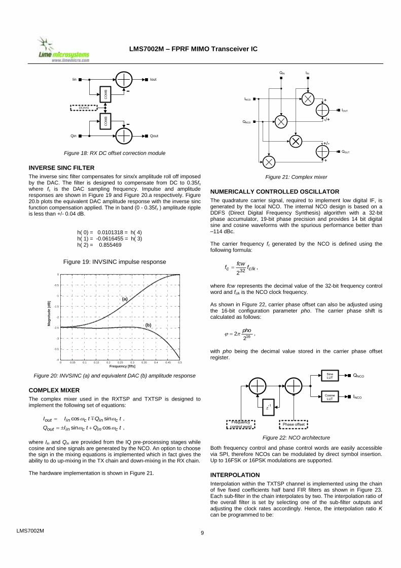
COMPLEX MIXER
The complex mixer used in the RXTSP and TXTSP is designed to implement the following set of equations:
tQtII cincinout sincos ,
tQtIQ cincinout cossin ,
where Iin and Qin are provided from the IQ pre-processing stages while cosine and sine signals are generated by the NCO. An option to choose the sign in the mixing equations is implemented which in fact gives the ability to do up-mixing in the TX chain and down-mixing in the RX chain. The hardware implementation is shown in Figure 21.
IINQIN
+
-/+
+
+/-
IOUT
QOUT
INCO
QNCO
Figure 21: Complex mixer
NUMERICALLY CONTROLLED OSCILLATOR
The quadrature carrier signal, required to implement low digital IF, is generated by the local NCO. The internal NCO design is based on a DDFS (Direct Digital Frequency Synthesis) algorithm with a 32-bit phase accumulator, 19-bit phase precision and provides 14 bit digital sine and cosine waveforms with the spurious performance better than –114 dBc. The carrier frequency fc generated by the NCO is defined using the following formula:
clkc ffcw
f322
,
where fcw represents the decimal value of the 32-bit frequency control word and fclk is the NCO clock frequency. As shown in Figure 22, carrier phase offset can also be adjusted using the 16-bit configuration parameter pho. The carrier phase shift is calculated as follows:
1622
pho ,
with pho being the decimal value stored in the carrier phase offset register.
Frequency
control word
Z-1
SineLUT
CosineLUT
Phase offset
INCO
QNCO
Figure 22: NCO architecture
Both frequency control and phase control words are easily accessible via SPI, therefore NCOs can be modulated by direct symbol insertion. Up to 16FSK or 16PSK modulations are supported.
INTERPOLATION
Interpolation within the TXTSP channel is implemented using the chain of five fixed coefficients half band FIR filters as shown in Figure 23. Each sub-filter in the chain interpolates by two. The interpolation ratio of the overall filter is set by selecting one of the sub-filter outputs and adjusting the clock rates accordingly. Hence, the interpolation ratio K can be programmed to be:
LMS7002M 10
LMS7002M – FPRF MIMO Transceiver IC
32or16,8,4,2,1K .
Interpolation by 1 is achieved by bypassing all the interpolation filters. The filters are designed to provide a wide signal pass band from DC to fp where:
K
ff clkp 27.0 , K = 2, 4, 8, 16, 32.
X
Y
clk1 clk2 clk3 clk4
MU
X
HB2c↑2HB2b↑2HB2a↑2HB1↑2
clk5
HB2d↑2
Figure 23: Programmable rate interpolation implemented by half band filters
h( 0) = -4.673e-05 = h(30)
h( 1) = 0 = h(29)
h( 2) = 0.000392914 = h(28)
h( 3) = 0 = h(27)
h( 4) = -0.00181007 = h(26)
h( 5) = 0 = h(25)
h( 6) = 0.00600147 = h(24)
h( 7) = 0 = h(23)
h( 8) = -0.0160789 = h(22)
h( 9) = 0 = h(21)
h(10) = 0.0378866 = h(20)
h(11) = 0 = h(19)
h(12) = -0.0882454 = h(18)
h(13) = 0 = h(17)
h(14) = 0.3119 = h(16)
h(15) = 0.5
Figure 24: HB1 impulse response
-140
-120
-100
-80
-60
-40
-20
0
20
0 0.05 0.1 0.15 0.2 0.25 0.3 0.35 0.4 0.45 0.5
Ma
gn
itu
de
[d
B]
Frequency
Figure 25: HB1 amplitude response
Only two different configurations are used within the filtering chain of Figure 23, HB1 and HB2. The impulse and amplitude response of HB1 are shown in Figure 24 and Figure 25, respectively. The remaining three filters (HB2A, HB2B and HB2C) are all the same with their coefficients and amplitude response given in Figure 26 and Figure 27, respectively. The overall interpolator provides image suppression of better than –108 dB with negligible amplitude distortion (pass band ripple is less than10
-5 dB).
h( 0) = -0.00164032 = h(14)
h( 1) = 0 = h(13)
h( 2) = 0.0138855 = h(12)
h( 3) = 0 = h(11)
h( 4) = -0.0630875 = h(10)
h( 5) = 0 = h( 9)
h( 6) = 0.300842 = h( 8)
h( 7) = 0.5
Figure 26: HB2 impulse response
-140
-120
-100
-80
-60
-40
-20
0
20
0 0.05 0.1 0.15 0.2 0.25 0.3 0.35 0.4 0.45 0.5
Ma
gn
itu
de [
dB
]
Frequency
Figure 27: HB2 amplitude response
DECIMATION
The decimation function is implemented using the same filters as in the case for interpolation although the hardware is simplified slightly by taking advantage of only having to provide every second sample at the sub-filters output. The filter chain is shown in Figure 28.
MU
X
HB2a ↓2
MU
X
HB2b ↓2
MU
X
HB2c ↓2 HB1 ↓2
X
Y
clk2 clk3 clk4 clk5
MU
X
MU
X
clk1
HB2d ↓2
Figure 28: Programmable rate decimation implemented by half band filters
Decimation ratio K can be programmed to be:
32or16,8,4,2,1K .
Decimation by 1 is achieved by bypassing all the decimation filters. Decimator performance is the same as the performance of the interpolator i.e. pass band is:
K
ff clkp 27.0 , K = 2, 4, 8, 16, 32,
alias suppression is better than –108 dB while in band amplitude distortion is negligible.
GENERAL PURPOSE FIR FILTERS
The LMS7002M features general purpose filters 1 and 2, which are based on a Multiply Accumulate (MAC) FIR architecture. They can implement up to a 40-tap filtering function and the coefficients are fully programmable via SPI. The hardware implementation does not impose the constraint for the filter impulse response to be symmetrical hence the filter phase response can but does not need to be ideally linear. Therefore, it can be used in general filtering, as well as nonlinear applications which can be used to implement phase equalization. The filter coefficients are stored in five 8x16-bit internal memory banks as two’s complement signed integers as shown in Figure 29 where L is related to the filter length N as follows:
5
NL .
Grey locations in Figure 29 highlight the memory registers which are set to zero for 5L > N. Evidently, the number of the filter taps N is limited by the size of the coefficients memory to:
LMS7002M 11
LMS7002M – FPRF MIMO Transceiver IC
408*5 N .
The following relationship should be satisfied:
KL , K being the interpolation or decimation ratio, for the MAC hardware to be able to produce output samples on time.
L
Memory Bank 0
loca
tions
Memory Bank 1 Memory Bank 4
Figure 29: General purpose FIR filter coefficients memory organisation
General purpose FIR filter 3 is composed of three filters running in parallel in order to increase its processing power hence it can implement the filters with:
12040*3 N .
It can be used as a channel select filter or for any other purpose which requires a larger number of filtering taps.
RECEIVED SIGNAL STRENGTH INDICATORS
A digital received signal strength indicator (RSSI) circuit calculates the level of the received complex signal (I + jQ) as follows:
22 QIRSSI .
The following approximation of the square root is implemented in the chip:
MNMMba ,5.0125.0max22 ,
where:
baN
baM
,min
,max
.
The same RSSI block is used within the digital AGC loop. If digital AGC is not required then the RSSI output can be provided back to the BB modem via SPI. In this way the BB can control RF and IF gain stages to implement analog AGC in which case the AGC loop is closed via the BB modem. There is also an RF RSSI block implemented in the RF front end connected to the input of the wideband LNA. This block can be used to detect the presence of large interferers so the BB modem can adjust RX gain stages very quickly to counteract such scenarios. The RF RSSI output is routed to I ADCs of RX channel 1 or RX channel 2. When the RSSI output is to be read, the main RX path of that channel should be disabled. The RSSI detects the input from -70 dBm to -20 dBm, corresponding to the full dynamic range of the ADC.
AUTOMATIC GAIN CONTROL
The structure of the digital automatic gain control loop is shown in Figure 30. The AGC loop functions as follows:
“Square root of two” (RSSI) block calculates the RMS of the AGC output.
This signal is averaged by the COMB filter. The averaging window size AVG is programmable via SPI.
An error signal is then calculated as the difference between the desired output signal level and the measured one. The desired amplitude level ADESIRED is programmable via SPI.
After the loop gain stage, the error is integrated to construct the digital VGAs gain control signal. Loop gain K is programmable via SPI.
VGAs gain cannot be negative and should not be zero either, hence max(1,x) module is provided in the feedback path.
errorMAX(1, X) Z-1 K/2N-1 COMB
N
AVGADESIREDK
IIN
QIN
IOUT
QOUT
Integrator Loop Gain Averaging
Filter
-
+
I2 + Q2
2
Figure 30: AGC architecture
Figure 31 illustrates two possible applications of the digital AGC. The first example (Figure 31.a) shows the case where the BB modem expects 4-bits instead of full 12-bit ADC output. In this case, ADESIRED loop parameter is set as shown in the figure, the gain of RF and IF stages are set for ADC not to produce full scale but ADESIRED level instead. The middle 4 bits are provided to BB. If the RF input signal level goes higher or lower, AGC will adapt the gain to keep its output at ADESIRED value so bits 7 to 4 will always contain 4 MSBs of the received signal. Since we have 4 bits on top and 4 bits below the middle 4 bits, the loop itself provides +/-24 dB automatic gain control range without using RF and IF gain stages.
To BB
11
10
9
8
7
6
5
4
3
2
1
0
ADESIRED
(a)
To BB
11
10
9
8
7
6
5
4
3
2
1
0
ADESIRED
(b)
Figure 31: Truncation to (a) 4 bits and (b) 10 bits
The second example shown in Figure 31.b is a more general case. The BB modem will receive 10-bits while the loop provides +/- 6 dB gain control range without engaging RF and IF gain blocks.
LIMELIGHTTM
DIGITAL IQ DATA INTERFACE
Description
The LMS7002M implements LimeLight™ digital IQ interface to the BB modem. LimeLight™ can be configured to run in one of the following three modes:
1. JESD207 mode 2. TRXIQ double data rate (DDR) mode 3. TRXIQ single data rate (SDR) mode
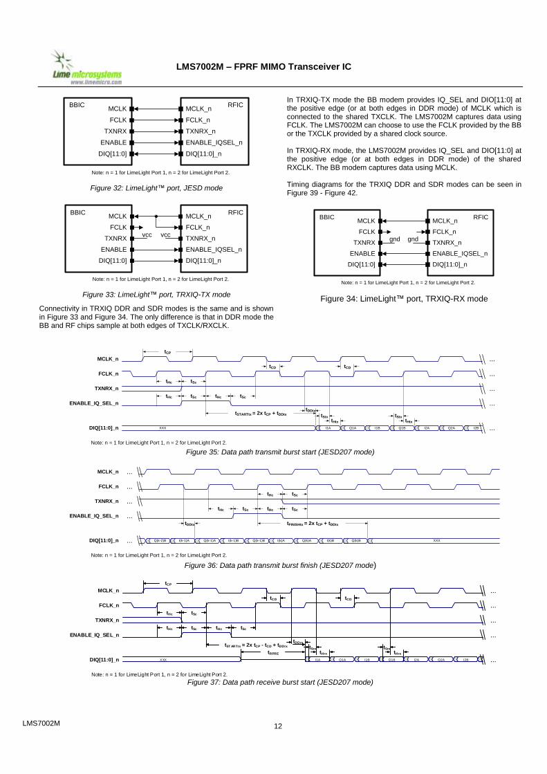
All three modes are capable of supporting both TDD and FDD operation. The data throughput of JESD207 and TRX DDR is high enough to connect to up to 2x2 MIMO BB modems. TRXIQ SDR mode is backward compatible to the LMS6002D digital IQ interface. Figure 32 shows typical connectivity between the LMS7002M and the BB modem with LimeLight™ running in JESD207 mode. LimeLight™ uses two such ports to support FDD. Signalling is defined by the JESD207 standard itself as specified by JEDEC. Timing diagrams for the JESD207 mode can be seen in Figure 35 - Figure 38.
LMS7002M 12
LMS7002M – FPRF MIMO Transceiver IC
Note: n = 1 for LimeLight Port 1, n = 2 for LimeLight Port 2.
MCLK_n
FCLK_n
TXNRX_n
ENABLE_IQSEL_n
DIQ[11:0]_n
RFICMCLK
FCLK
TXNRX
ENABLE
DIQ[11:0]
BBIC
Figure 32: LimeLight™ port, JESD mode
vccvcc
Note: n = 1 for LimeLight Port 1, n = 2 for LimeLight Port 2.
MCLK_n
FCLK_n
TXNRX_n
ENABLE_IQSEL_n
DIQ[11:0]_n
RFICMCLK
FCLK
TXNRX
ENABLE
DIQ[11:0]
BBIC
Figure 33: LimeLight™ port, TRXIQ-TX mode
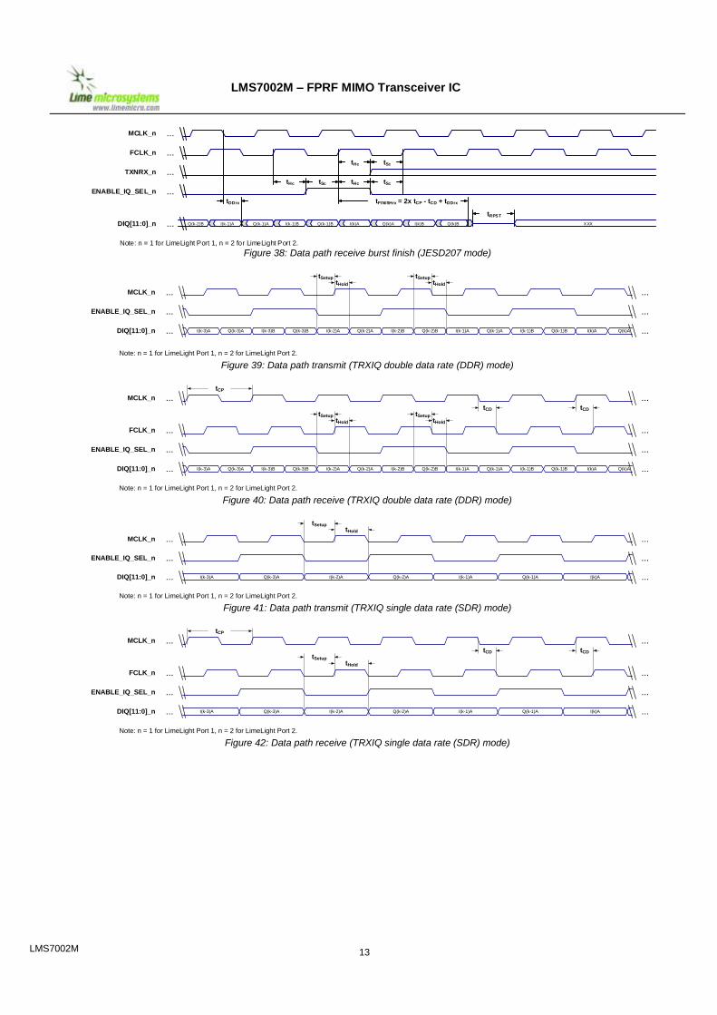
Connectivity in TRXIQ DDR and SDR modes is the same and is shown in Figure 33 and Figure 34. The only difference is that in DDR mode the BB and RF chips sample at both edges of TXCLK/RXCLK.
In TRXIQ-TX mode the BB modem provides IQ_SEL and DIO[11:0] at the positive edge (or at both edges in DDR mode) of MCLK which is connected to the shared TXCLK. The LMS7002M captures data using FCLK. The LMS7002M can choose to use the FCLK provided by the BB or the TXCLK provided by a shared clock source. In TRXIQ-RX mode, the LMS7002M provides IQ_SEL and DIO[11:0] at the positive edge (or at both edges in DDR mode) of the shared RXCLK. The BB modem captures data using MCLK. Timing diagrams for the TRXIQ DDR and SDR modes can be seen in Figure 39 - Figure 42.
gndgnd
Note: n = 1 for LimeLight Port 1, n = 2 for LimeLight Port 2.
MCLK_n
FCLK_n
TXNRX_n
ENABLE_IQSEL_n
DIQ[11:0]_n
RFICMCLK
FCLK
TXNRX
ENABLE
DIQ[11:0]
BBIC
Figure 34: LimeLight™ port, TRXIQ-RX mode
ENABLE_IQ_SEL_n
MCLK_n
FCLK_n
TXNRX_n
DIQ[11:0]_n
tCP
Q1AI1A I1B Q1B I2A
tHc
tHc
tSc
tSc tSctHc
tDDtx
tStx
tHtx
tStx
tHtx
tSTARTtx = 2x tCP + tDDtx
XXX
tCD tCD
Q2A I2B ...
...
...
...
...
Note: n = 1 for LimeLight Port 1, n = 2 for LimeLight Port 2. Figure 35: Data path transmit burst start (JESD207 mode)
Q(k-2)B
MCLK_n
FCLK_n
DIQ[11:0]_n
TXNRX_n
ENABLE_IQ_SEL_n
I(k-1)A Q(k-1)A I(k-1)B Q(k-1)B I(k)A Q(k)A I(k)B Q(k)B
...
...
...
...
...
tHc
tHctHc
tSc
tSctSc
tDDtx tFINISHtx = 2x tCP + tDDtx
XXX
Note: n = 1 for LimeLight Port 1, n = 2 for LimeLight Port 2. Figure 36: Data path transmit burst finish (JESD207 mode)
ENABLE_IQ_SEL_n
MCLK_n
FCLK_n
TXNRX_n
DIQ[11:0]_n
tCP
Q1AI1A I1B Q1B I2A
tHc
tHc
tSc
tSc tSctHc
tST ARTrx = 2x tCP - tCD + tDDrx
XXX
tCD tCD
Q2A I2B ...
...
...
...
...
tRPRE
tDDrx
tHrx tHrx
tSrx tSrx
Note: n = 1 for LimeLight Port 1, n = 2 for LimeLight Port 2. Figure 37: Data path receive burst start (JESD207 mode)
LMS7002M 13
LMS7002M – FPRF MIMO Transceiver IC
Q(k-2)B
MCLK_n
FCLK_n
DIQ[11:0]_n
TXNRX_n
ENABLE_IQ_SEL_n
I(k-1)A Q(k-1)A I(k-1)B Q(k-1)B I(k)A Q(k)A I(k)B Q(k)B
...
...
...
...
...
tHc
tHctHc
tSc
tSctSc
Note: n = 1 for LimeLight Port 1, n = 2 for LimeLight Port 2.
tFINISHrx = 2x tCP - tCD + tDDrx
XXX
tDDrx
tRPST
Figure 38: Data path receive burst finish (JESD207 mode)
ENABLE_IQ_SEL_n
MCLK_n
DIQ[11:0]_n
...
......
...
... I(k-3)A Q(k-3)A I(k-3)B Q(k-3)B I(k-2)A I(k-1)A I(k)AQ(k-2)A Q(k-1)A Q(k)AI(k-2)B I(k-1)BQ(k-2)B Q(k-1)B ...
tSetup tSetup
tHold tHold
Note: n = 1 for LimeLight Port 1, n = 2 for LimeLight Port 2. Figure 39: Data path transmit (TRXIQ double data rate (DDR) mode)
ENABLE_IQ_SEL_n
MCLK_n
FCLK_n
DIQ[11:0]_n
tCP
...
...
......
...
...
... I(k-3)A Q(k-3)A I(k-3)B Q(k-3)B I(k-2)A I(k-1)A I(k)AQ(k-2)A Q(k-1)A Q(k)AI(k-2)B I(k-1)BQ(k-2)B Q(k-1)B
tCD tCD
tSetup tSetup
tHold tHold
...
Note: n = 1 for LimeLight Port 1, n = 2 for LimeLight Port 2. Figure 40: Data path receive (TRXIQ double data rate (DDR) mode)
ENABLE_IQ_SEL_n
MCLK_n
DIQ[11:0]_n
...
......
...
... I(k-3)A Q(k-3)A I(k-2)A I(k-1)A I(k)AQ(k-2)A Q(k-1)A
tSetup
tHold
...
Note: n = 1 for LimeLight Port 1, n = 2 for LimeLight Port 2. Figure 41: Data path transmit (TRXIQ single data rate (SDR) mode)
ENABLE_IQ_SEL_n
MCLK_n
FCLK_n
DIQ[11:0]_n
tCP
...
...
......
...
...
... I(k-3)A Q(k-3)A I(k-2)A I(k-1)A I(k)AQ(k-2)A Q(k-1)A
tCD tCD
tSetup
tHold
...
Note: n = 1 for LimeLight Port 1, n = 2 for LimeLight Port 2. Figure 42: Data path receive (TRXIQ single data rate (SDR) mode)
LMS7002M 14
LMS7002M – FPRF MIMO Transceiver IC
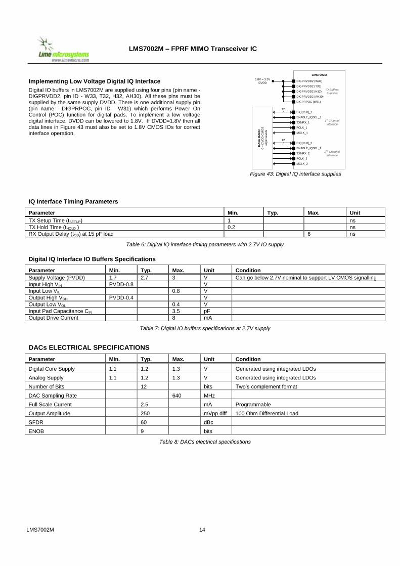
Implementing Low Voltage Digital IQ Interface
Digital IO buffers in LMS7002M are supplied using four pins (pin name - DIGPRVDD2, pin ID - W33, T32, H32, AH30). All these pins must be supplied by the same supply DVDD. There is one additional supply pin (pin name - DIGPRPOC, pin ID - W31) which performs Power On Control (POC) function for digital pads. To implement a low voltage digital interface, DVDD can be lowered to 1.8V. If DVDD=1.8V then all data lines in Figure 43 must also be set to 1.8V CMOS IOs for correct interface operation.
1.8V – 3.3V
DVDDDIGPRVDD2 (W33)
DIGPRVDD2 (T32)
DIGPRVDD2 (H32)
DIGPRVDD2 (AH30)
DIGPRPOC (W31)
IO Buffers
Supplies
BA
SE
BA
ND
0 –
DV
DD
CM
OS
Lo
gic
Le
ve
ls
LMS7002M
/12
DIQ[11:0]_1
ENABLE_IQSEL_1
TXNRX_1
FCLK_1
MCLK_1
/12
DIQ[11:0]_2
ENABLE_IQSEL_2
TXNRX_2
FCLK_2
MCLK_2
1st Channel
Interface
2nd
Channel
Interface
Figure 43: Digital IQ interface supplies
IQ Interface Timing Parameters
Parameter Min. Typ. Max. Unit
TX Setup Time (tSETUP) 1 ns
TX Hold Time (tHOLD ) 0.2 ns
RX Output Delay (tOD) at 15 pF load 6 ns
Table 6: Digital IQ interface timing parameters with 2.7V IO supply
Digital IQ Interface IO Buffers Specifications
Parameter Min. Typ. Max. Unit Condition
Supply Voltage (PVDD) 1.7 2.7 3 V Can go below 2.7V nominal to support LV CMOS signalling
Input High VIH PVDD-0.8 V
Input Low VIL 0.8 V
Output High VOH PVDD-0.4 V
Output Low VOL 0.4 V
Input Pad Capacitance CIN 3.5 pF
Output Drive Current 8 mA
Table 7: Digital IO buffers specifications at 2.7V supply
DACs ELECTRICAL SPECIFICATIONS
Parameter Min. Typ. Max. Unit Condition
Digital Core Supply 1.1 1.2 1.3 V Generated using integrated LDOs
Analog Supply 1.1 1.2 1.3 V Generated using integrated LDOs
Number of Bits 12 bits Two’s complement format
DAC Sampling Rate 640 MHz
Full Scale Current 2.5 mA Programmable
Output Amplitude 250 mVpp diff 100 Ohm Differential Load
SFDR 60 dBc
ENOB 9 bits
Table 8: DACs electrical specifications
LMS7002M 15
LMS7002M – MIMO Multi-Band Multi-Standard
Transceiver IC
ADCs ELECTRICAL SPECIFICATIONS
Parameter Min. Typ. Max. Unit Condition
Digital Core Supply 1.1 1.2 1.3 V Generated using integrated LDOs
Analog Supply 1.1 1.2 1.3 V Generated using integrated LDOs
Number of Bits 12 bits Two’s complement format
ADC Sampling Rate 160 MHz
Input Amplitude 2.4 Vpp Differential
Input Common Mode Voltage 1.2 V Input buffer off
Input Impedance 2 kOhm
ENOB 9 bits
Table 9: ADCs electrical specifications
SERIAL PORT INTERFACE
Description
The functionality of the LMS7002M transceiver is fully controlled by a set of internal registers which can be accessed through a serial port interface. Both write and read SPI operations are supported. The serial port can be configured to run in 3 or 4 wire mode with the following pins used:
SEN serial port enable, active low
SCLK serial clock, positive edge sensitive
SDIO serial data in/out in 3 wire mode serial data input in 4 wire mode
SDO serial data out in 4 wire mode don’t care in 3 wire mode
Serial port key features:
32 SPI clock cycles are required to complete a write operation.
32 SPI clock cycles are required to complete a read operation.
Multiple write/read operations are possible without toggling serial port enable signal.
All configuration registers are 16-bit wide. Write/read sequence consists of 16-bit instruction followed by 16-bit data to write or read. MSB of the instruction bit stream is used as SPI command where CMD = 1 for write and CMD = 0 for read. Next 4 bits are reserved (Reserved[3:0]) and must be zeroes. Next 5 bits represent module address (Maddress[4:0]) since the LMS7002M configuration registers are divided into logical blocks as shown in Table 11. The remaining 6 bits of the instruction are used to address particular registers (Reg[5:0]) within the block. Maddress and Reg compiles global 11-bit register address when concatenated ((Maddress << 6) | Reg). The write/read cycle waveforms are shown in Figure 44, Figure 45 and Figure 46. Note that the write operation is the same for both 3-wire and 4-wire modes. Although not shown in the figures, multiple write/read is possible by repeating the instruction/data sequence while keeping SEN low.
SPI Timing Parameters
Parameter Min. Typ. Max. Unit
Clock Frequency, 4-wire mode 3-wire mode
50 MHz
20 MHz
Enable Setup Time (tES) 2 ns
Enable Hold Time (tEH) 0.2 ns
Data Setup Time (tDS) 1 ns
Data Hold Time (tDH) 0.2 ns
Data Output Delay (tOD) at 12pF load 9 ns
Table 10: SPI timing parameters at 2.7V IO supply
Write Operation
SCLK Don’t care
SEN
SDIO Don’t care A141 A13 A12 A11 A10 A9 A8 A7 A6 A5 A4 A3 A2 A1 A0 D15 D14 D13 D12 D11 D10 D9 D8 D7 D6 D5 D4 D3 D2 D1 D0
Write instruction Data
Don’t care
Don’t care
tES tDS tDHtEH
Figure 44: SPI write cycle, 3-wire and 4-wire modes
LMS7002M 16
LMS7002M – FPRF MIMO Transceiver IC
Read Operation
SCLK Don’t care
SEN
SDIO Don’t care A140 A13 A12 A11 A10 A9 A8 A7 A6 A5 A4 A3 A2 A1 A0
Read instruction
Don’t care
Don’t care
tES tDS tDHtEH
SDO Don’t care
Output Data
D15 D14 D13 D12 D11 D10 D9 D8 D7 D6 D5 D4 D3 D2 D1 D0 Don’t care
tOD
Figure 45: SPI read cycle, 4-wire mode (default)
SCLK Don’t care
SEN
SDIO Don’t care A140 A13 A12 A11 A10 A9 A8 A7 A6 A5 A4 A3 A2 A1 A0
Read instruction
Don’t care
tES tDS tDHtEH
Output Data
D15 D14 D13 D12 D11 D10 D9 D8 D7 D6 D5 D4 D3 D2 D1 D0 Don’t care
tOD
Figure 46: SPI read cycle, 3-wire mode
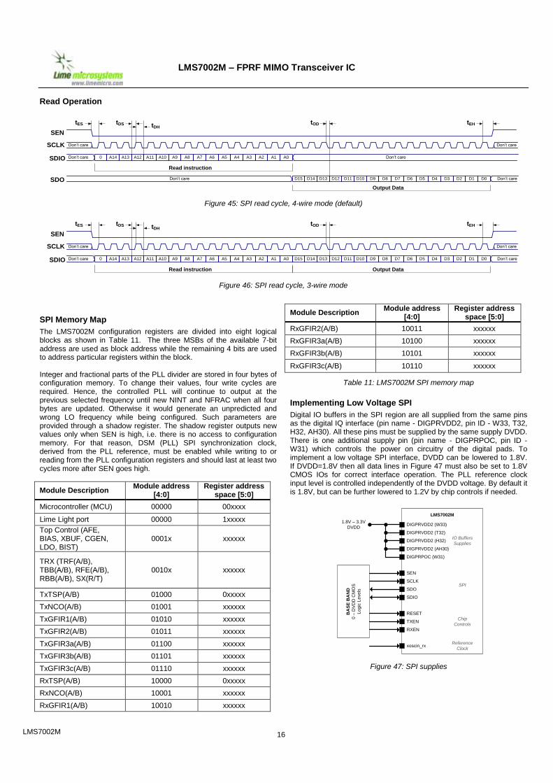
SPI Memory Map
The LMS7002M configuration registers are divided into eight logical blocks as shown in Table 11. The three MSBs of the available 7-bit address are used as block address while the remaining 4 bits are used to address particular registers within the block. Integer and fractional parts of the PLL divider are stored in four bytes of configuration memory. To change their values, four write cycles are required. Hence, the controlled PLL will continue to output at the previous selected frequency until new NINT and NFRAC when all four bytes are updated. Otherwise it would generate an unpredicted and wrong LO frequency while being configured. Such parameters are provided through a shadow register. The shadow register outputs new values only when SEN is high, i.e. there is no access to configuration memory. For that reason, DSM (PLL) SPI synchronization clock, derived from the PLL reference, must be enabled while writing to or reading from the PLL configuration registers and should last at least two cycles more after SEN goes high.
Module Description Module address
[4:0] Register address
space [5:0]
Microcontroller (MCU) 00000 00xxxx
Lime Light port 00000 1xxxxx
Top Control (AFE, BIAS, XBUF, CGEN, LDO, BIST)
0001x xxxxxx
TRX (TRF(A/B), TBB(A/B), RFE(A/B), RBB(A/B), SX(R/T)
0010x xxxxxx
TxTSP(A/B) 01000 0xxxxx
TxNCO(A/B) 01001 xxxxxx
TxGFIR1(A/B) 01010 xxxxxx
TxGFIR2(A/B) 01011 xxxxxx
TxGFIR3a(A/B) 01100 xxxxxx
TxGFIR3b(A/B) 01101 xxxxxx
TxGFIR3c(A/B) 01110 xxxxxx
RxTSP(A/B) 10000 0xxxxx
RxNCO(A/B) 10001 xxxxxx
RxGFIR1(A/B) 10010 xxxxxx
Module Description Module address
[4:0] Register address
space [5:0]
RxGFIR2(A/B) 10011 xxxxxx
RxGFIR3a(A/B) 10100 xxxxxx
RxGFIR3b(A/B) 10101 xxxxxx
RxGFIR3c(A/B) 10110 xxxxxx
Table 11: LMS7002M SPI memory map
Implementing Low Voltage SPI
Digital IO buffers in the SPI region are all supplied from the same pins as the digital IQ interface (pin name - DIGPRVDD2, pin ID - W33, T32, H32, AH30). All these pins must be supplied by the same supply DVDD. There is one additional supply pin (pin name - DIGPRPOC, pin ID - W31) which controls the power on circuitry of the digital pads. To implement a low voltage SPI interface, DVDD can be lowered to 1.8V. If DVDD=1.8V then all data lines in Figure 47 must also be set to 1.8V CMOS IOs for correct interface operation. The PLL reference clock input level is controlled independently of the DVDD voltage. By default it is 1.8V, but can be further lowered to 1.2V by chip controls if needed.
1.8V – 3.3V
DVDDDIGPRVDD2 (W33)
DIGPRVDD2 (T32)
DIGPRVDD2 (H32)
DIGPRVDD2 (AH30)
DIGPRPOC (W31)
IO Buffers
Supplies
BA
SE
BA
ND
0 –
DV
DD
CM
OS
Lo
gic
Le
ve
ls
SEN
SCLK
SDO
SDIO
RESET
TXEN
RXEN
xoscin_rx
SPI
Chip
Controls
Reference
Clock
LMS7002M
Figure 47: SPI supplies
LMS7002M 17
LMS7002M – FPRF MIMO Transceiver IC
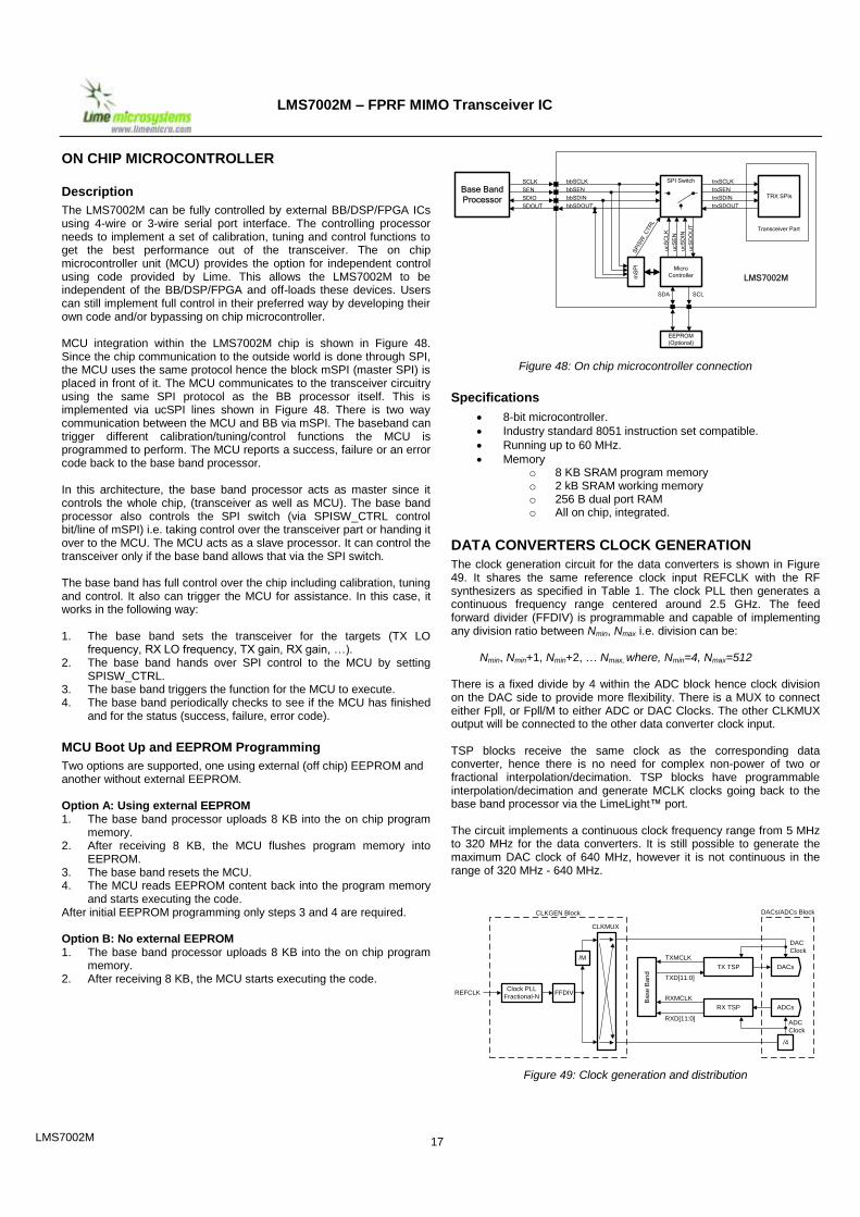
ON CHIP MICROCONTROLLER
Description
The LMS7002M can be fully controlled by external BB/DSP/FPGA ICs using 4-wire or 3-wire serial port interface. The controlling processor needs to implement a set of calibration, tuning and control functions to get the best performance out of the transceiver. The on chip microcontroller unit (MCU) provides the option for independent control using code provided by Lime. This allows the LMS7002M to be independent of the BB/DSP/FPGA and off-loads these devices. Users can still implement full control in their preferred way by developing their own code and/or bypassing on chip microcontroller. MCU integration within the LMS7002M chip is shown in Figure 48. Since the chip communication to the outside world is done through SPI, the MCU uses the same protocol hence the block mSPI (master SPI) is placed in front of it. The MCU communicates to the transceiver circuitry using the same SPI protocol as the BB processor itself. This is implemented via ucSPI lines shown in Figure 48. There is two way communication between the MCU and BB via mSPI. The baseband can trigger different calibration/tuning/control functions the MCU is programmed to perform. The MCU reports a success, failure or an error code back to the base band processor. In this architecture, the base band processor acts as master since it controls the whole chip, (transceiver as well as MCU). The base band processor also controls the SPI switch (via SPISW_CTRL control bit/line of mSPI) i.e. taking control over the transceiver part or handing it over to the MCU. The MCU acts as a slave processor. It can control the transceiver only if the base band allows that via the SPI switch. The base band has full control over the chip including calibration, tuning and control. It also can trigger the MCU for assistance. In this case, it works in the following way: 1. The base band sets the transceiver for the targets (TX LO
frequency, RX LO frequency, TX gain, RX gain, …). 2. The base band hands over SPI control to the MCU by setting
SPISW_CTRL. 3. The base band triggers the function for the MCU to execute. 4. The base band periodically checks to see if the MCU has finished
and for the status (success, failure, error code).
MCU Boot Up and EEPROM Programming
Two options are supported, one using external (off chip) EEPROM and another without external EEPROM. Option A: Using external EEPROM 1. The base band processor uploads 8 KB into the on chip program
memory. 2. After receiving 8 KB, the MCU flushes program memory into
EEPROM. 3. The base band resets the MCU. 4. The MCU reads EEPROM content back into the program memory
and starts executing the code. After initial EEPROM programming only steps 3 and 4 are required. Option B: No external EEPROM 1. The base band processor uploads 8 KB into the on chip program
memory. 2. After receiving 8 KB, the MCU starts executing the code.
SEN
SCLK
SDIO
SDOUT
SP
ISW
_C
TR
L
ucS
EN
ucS
CL
K
ucS
DIN
ucS
DO
UT
bbSEN
bbSCLK
bbSDIN
bbSDOUT
trxSEN
trxSCLK
trxSDIN
trxSDOUT
Micro
ControllermS
PI
SPI Switch
TRX SPIs
Transceiver Part
EEPROM
(Optional)
SCLSDA
LMS7002M
Base Band
Processor
Figure 48: On chip microcontroller connection
Specifications
8-bit microcontroller.
Industry standard 8051 instruction set compatible.
Running up to 60 MHz.
Memory o 8 KB SRAM program memory o 2 kB SRAM working memory o 256 B dual port RAM o All on chip, integrated.
DATA CONVERTERS CLOCK GENERATION
The clock generation circuit for the data converters is shown in Figure 49. It shares the same reference clock input REFCLK with the RF synthesizers as specified in Table 1. The clock PLL then generates a continuous frequency range centered around 2.5 GHz. The feed forward divider (FFDIV) is programmable and capable of implementing any division ratio between Nmin, Nmax i.e. division can be:
Nmin, Nmin+1, Nmin+2, … Nmax, where, Nmin=4, Nmax=512 There is a fixed divide by 4 within the ADC block hence clock division on the DAC side to provide more flexibility. There is a MUX to connect either Fpll, or Fpll/M to either ADC or DAC Clocks. The other CLKMUX output will be connected to the other data converter clock input. TSP blocks receive the same clock as the corresponding data converter, hence there is no need for complex non-power of two or fractional interpolation/decimation. TSP blocks have programmable interpolation/decimation and generate MCLK clocks going back to the base band processor via the LimeLight™ port. The circuit implements a continuous clock frequency range from 5 MHz to 320 MHz for the data converters. It is still possible to generate the maximum DAC clock of 640 MHz, however it is not continuous in the range of 320 MHz - 640 MHz.
TXMCLK
RXMCLKBa
se
Ba
nd
DACs
ADCsRX TSP
TX TSP
DAC
Clock
ADC
Clock
RXD[11:0]
TXD[11:0]
DACs/ADCs Block
/M
/4
CLKMUX
FFDIVClock PLL
Fractional-NREFCLK
CLKGEN Block
Figure 49: Clock generation and distribution
LMS7002M 18
LMS7002M – FPRF MIMO Transceiver IC
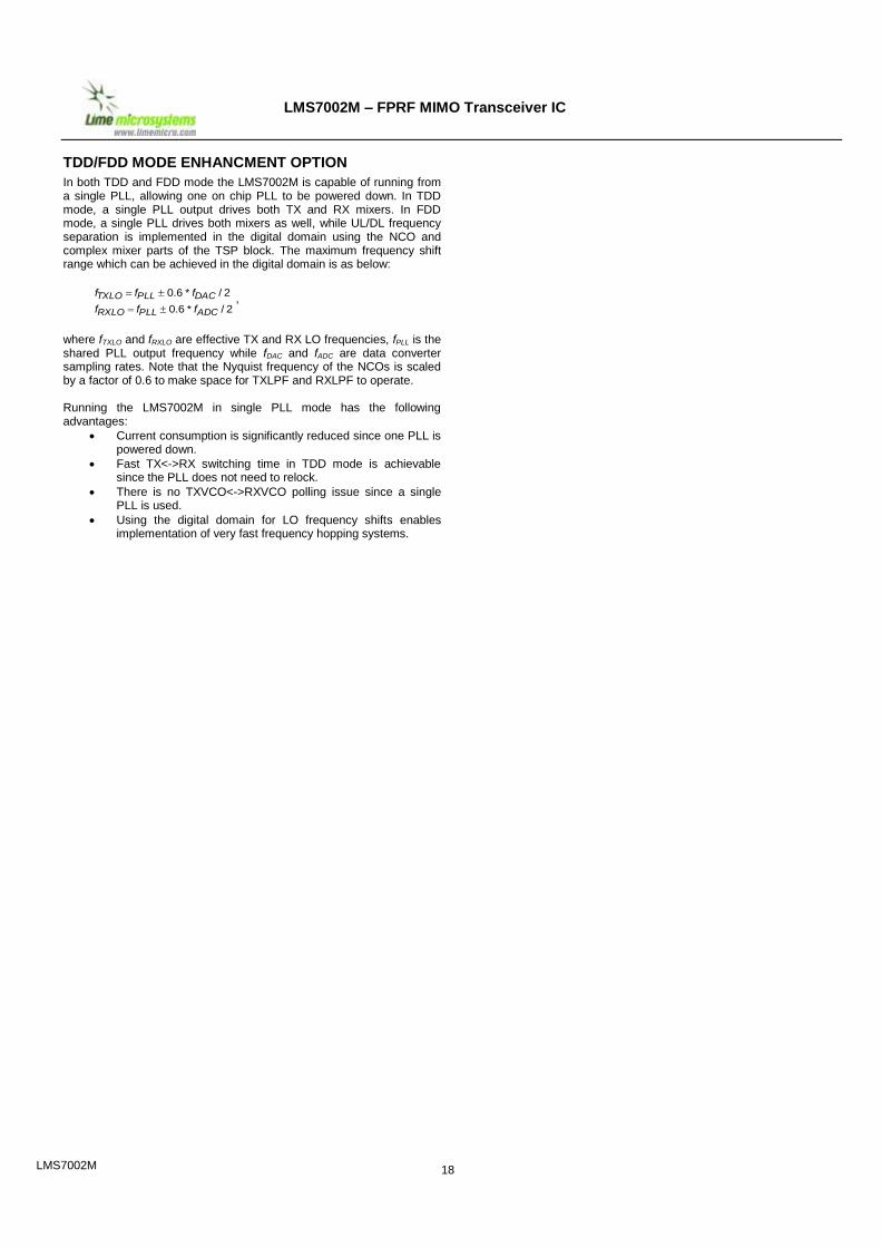
TDD/FDD MODE ENHANCMENT OPTION
In both TDD and FDD mode the LMS7002M is capable of running from a single PLL, allowing one on chip PLL to be powered down. In TDD mode, a single PLL output drives both TX and RX mixers. In FDD mode, a single PLL drives both mixers as well, while UL/DL frequency separation is implemented in the digital domain using the NCO and complex mixer parts of the TSP block. The maximum frequency shift range which can be achieved in the digital domain is as below:
2/*6.0
2/*6.0
ADCPLLRXLO
DACPLLTXLO
fff
fff
,
where fTXLO and fRXLO are effective TX and RX LO frequencies, fPLL is the shared PLL output frequency while fDAC and fADC are data converter sampling rates. Note that the Nyquist frequency of the NCOs is scaled by a factor of 0.6 to make space for TXLPF and RXLPF to operate. Running the LMS7002M in single PLL mode has the following advantages:
Current consumption is significantly reduced since one PLL is powered down.
Fast TX<->RX switching time in TDD mode is achievable since the PLL does not need to relock.
There is no TXVCO<->RXVCO polling issue since a single PLL is used.
Using the digital domain for LO frequency shifts enables implementation of very fast frequency hopping systems.
LMS7002M 19
LMS7002M – FPRF MIMO Transceiver IC
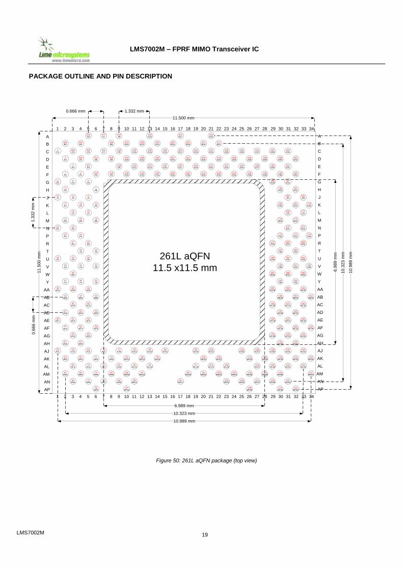
PACKAGE OUTLINE AND PIN DESCRIPTION
1
B
C
D
E
F
G
H
J
K
L
M
N
P
R
T
U
V
W
Y
AA
AB
AC
AD
AE
AF
AG
AH
AJ
AK
AL
AM
AN
AP
2 3 4 5 6 7 8 9 10 11 12 13 14 15 16 17 18 19 20 21 22 23 24 25 26 27 28 29 30 31 32 33 34
20M4
22N3
21M2
15L5
23N1
18M6
19L3
25P2
27R3
29T4
24P4
26R5
28T6
34V4
36W3
33V2
30U5
35V6
31U3
32U1
37Y2
41AA3
39AA1
43AB2
44AB4
40Y6
38Y4
42AA5
46AB6
50AD4
51AE3
47AD2
48AC5
49AE1
53AD6
54AE5
45AC3
52
AF2
56AG3
57AH2
61AH4
59AF6
55AF4
60AG5
252A5
260B2
258C3
1C1
2D2
261D4
256B4
255C5
254D6
4F4
8G3
7F2
257E5
11G1
259F6
5G5
3E3
12H2
13J3
16J1
17K2
14K4
6H6
9J5
10K6
65AK4
66AL3
63AK2
71AK6
70 AL5
62AJ3
58AJ1
67AM2
68AN3
74AM6
69AM4
73AN5
78AP6
126AK30
120AL29
124AJ29
119AK28
115AM28
117AP30
121AM30
116AN29
110AM26
113AK26
111AN27
112AJ25
109AP26
108AN25
114AL27
118AJ27
106AL23
105AK22
103AM22
107AM24
104AN23
99AM20
97AL19
100AK20
98AJ19
101AL21
102AJ21
96AM18
95AN17
92AL13
93AK14
90AJ13
94AJ15
133AK34
127AM34
125AL31
129AK32
130AJ31
123AP32
122AN31
128AL33
134AJ33
88AK12
86AL11
83AJ11
82AK10
85AM10
91AM12
89AN11
87AP10
80AM8
75AL7
76AK8
84AN9
72 AJ7
79AN7
81AL9
77AJ9
188F32
187G31
190F30
189G29
191E31
195E29
186H30
184J31
183K30
181K32
185H32
182J33
179K34
176M32
175N31
178M30
177L33
174N33
180L31
173P30
169R31
171R29
167T30
166T32
170P34
172P32
168R33
161V32
158W31
160V30
163U33
157W29
162V34
159W33
164U31
165U29
155Y30
153AA31
151AA29
148AB30
150AB32
156Y32
154AA33
152AB34
193C31
197C29
194D30
192D32
146AD32
141AE31
142AD30
149AC33
138AE29
144AE33
147AC31
145AC29
137AF30
136AG31
132AG29
131AH30
135AH32
143AF34
140AF32
139AG33
198D28
196F28
202D26
205C25
199E27
200F26
203E25
201C27
209C23
211B22
210D22
204F24
206D24
207E23
208F22
216D20
219C19
217B20
212E21
214F20
218E19
213C21
215A21
222B18
224C17
223A17
226B16
227D16
220F18
221D18
225E17
228F16
232D14
235C13
231B14
230E15
233A13
234F14
237E13
229C15
236B12
239C11
241B10
244D10
240F12
238D12
243E11
248F10
250D8
251C7
246B8
249E9
247A7
253F8
245C9
242A9A
1 2 3 4 5 6 7 8 9 10 11 12 13 14 15 16 17 18 19 20 21 22 23 24 25 26 27 28 29 30 31 32 33 34
64AJ5
B
C
D
E
F
G
H
J
K
L
M
N
P
R
T
U
V
W
Y
AA
AB
AC
AD
AE
AF
AG
AH
AJ
AK
AL
AM
AN
AP
A
11
.50
0 m
m
1.3
32
mm
0.6
66
mm
11.500 mm
1.332 mm0.666 mm
10.989 mm
10.323 mm
6.989 mm
10
.98
9 m
m
10.3
23
mm
6.9
89
mm261L aQFN
11.5 x11.5 mm
Figure 50: 261L aQFN package (top view)
LMS7002M 20
LMS7002M – FPRF MIMO Transceiver IC
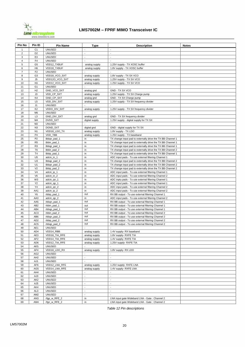
Pin No Pin ID Pin Name Type Description Notes
1 C1 UNUSED - -
2 D2 UNUSED - -
3 E3 UNUSED - -
4 F4 UNUSED - -
5 G5 VDD12_TXBUF analog supply 1.25V supply - TX XOSC buffer
6 H6 VDD18_TXBUF analog supply 1.8V supply - TX XOSC buffer
7 F2 UNUSED - -
8 G3 VDD18_VCO_SXT analog supply 1.8V supply - TX SX VCO
9 J5 VDD12O_VCO_SXT analog supply 1.25V supply - TX SX VCO
10 K6 VDD12_VCO_SXT analog supply 1.25V supply - TX SX VCO
11 G1 UNUSED - -
12 H2 GND_VCO_SXT analog gnd GND - TX SX VCO
13 J3 VDD_CP_SXT analog supply 1.25V supply - TX SX Charge pump
14 K4 GND_CP_SXT analog gnd GND - TX SX Charge pump
15 L5 VDD_DIV_SXT analog supply 1.25V supply - TX SX frequency divider
16 J1 UNUSED - -
17 K2 VDDO_DIV_SXT analog supply 1.25V supply - TX SX frequency divider
18 M6 UNUSED - -
19 L3 GND_DIV_SXT analog gnd GND - TX SX frequency divider
20 M4 DVDD_SXT digital supply 1.25V supply - digital supply for TX SX
21 M2 UNUSED - -
22 N3 DGND_SXT digital gnd GND - digital supply for TX SX
23 N1 VDD18_LDO_TX analog supply 1.8V supply - TX LDO
24 P4 VDD_TBB analog supply 1.25V supply - TX baseband
25 P2 tbbqn_pad_1 in TX change input pad to externally drive the TX BB Channel 1
26 R5 tbbin_pad_1 in TX change input pad to externally drive the TX BB Channel 1
27 R3 tbbqp_pad_1 in TX change input pad to externally drive the TX BB Channel 1
28 T6 tbbin_pad_2 in TX change input pad to externally drive the TX BB Channel 2
29 T4 tbbip_pad_1 in TX change input pad to externally drive the TX BB Channel 1
30 U5 adcin_in_1 in ADC input pads - To use external filtering Channel 1
31 U3 tbbqp_pad_2 in TX change input pad to externally drive the TX BB Channel 2
32 U1 tbbqn_pad_2 in TX change input pad to externally drive the TX BB Channel 2
33 V2 tbbip_pad_2 in TX change input pad to externally drive the TX BB Channel 2
34 V4 adcin_ip_1 in ADC input pads - To use external filtering Channel 1
35 V6 adcin_in_2 in ADC input pads - To use external filtering Channel 2
36 W3 adcin_qn_1 in ADC inptu pads - To use external filtering Channel 1
37 Y2 adcin_qp_1 in ADC input pads - To use external filtering Channel 1
38 Y4 adcin_qn_2 in ADC input pads - To use external filtering Channel 2
39 AA1 adcin_ip_2 in ADC input pads - To use external filtering Channel 2
40 Y6 rbbip_pad_1 out RX BB output - To use external filtering Channel 1
41 AA3 adcin_qp_2 in ADC input pads - To use external filtering Channel 2
42 AA5 rbbqn_pad_1 out RX BB output - To use external filtering Channel 1
43 AB2 rbbin_pad_1 out RX BB output - To use external filtering Channel 1
44 AB4 rbbqp_pad_1 out RX BB output - To use external filtering Channel 1
45 AC3 rbbin_pad_2 out RX BB output - To use external filtering Channel 2
46 AB6 rbbqn_pad_2 out RX BB output - To use external filtering Channel 2
47 AD2 rbbip_pad_2 out RX BB output - To use external filtering Channel 2
48 AC5 rbbqp_pad_2 out RX BB output - To use external filtering Channel 2
49 AE1 UNUSED - -
50 AD4 VDD14_RBB analog supply 1.4V supply- RX baseband
51 AE3 VDD18_TIA_RFE analog supply 1.8V supply- RXFE TIA
52 AF2 VDD14_TIA_RFE analog supply 1.4V supply- RXFE TIA
53 AD6 VDD12_TIA_RFE analog supply 1.25V supply- RXFE TIA
54 AE5 UNUSED - -
55 AF4 VDD18_LDO_RX analog supply 1.8V supply- RX LDO
56 AG2 UNUSED - -
57 AH2 UNUSED - -
58 AJ1 UNUSED - -
59 AF6 VDD12_LNA_RFE analog supply 1.25V supply- RXFE LNA
60 AG5 VDD14_LNA_RFE analog supply 1.4V supply- RXFE LNA
61 AH4 UNUSED - -
62 AJ3 UNUSED - -
63 AK2 UNUSED - -
64 AJ5 UNUSED - -
65 AK4 UNUSED - -
66 AL3 UNUSED - -
67 AM2 UNUSED - -
68 AN3 rfgp_w_RFE_2 in LNA input gate Wideband LNA - Gate : Channel 2
69 AM4 rfgn_w_RFE_2 in LNA input gate Wideband LNA - Gate : Channel 2
Table 12 Pin descriptions
LMS7002M 21
LMS7002M – FPRF MIMO Transceiver IC
Pin No Pin ID Pin Name Type Description Notes
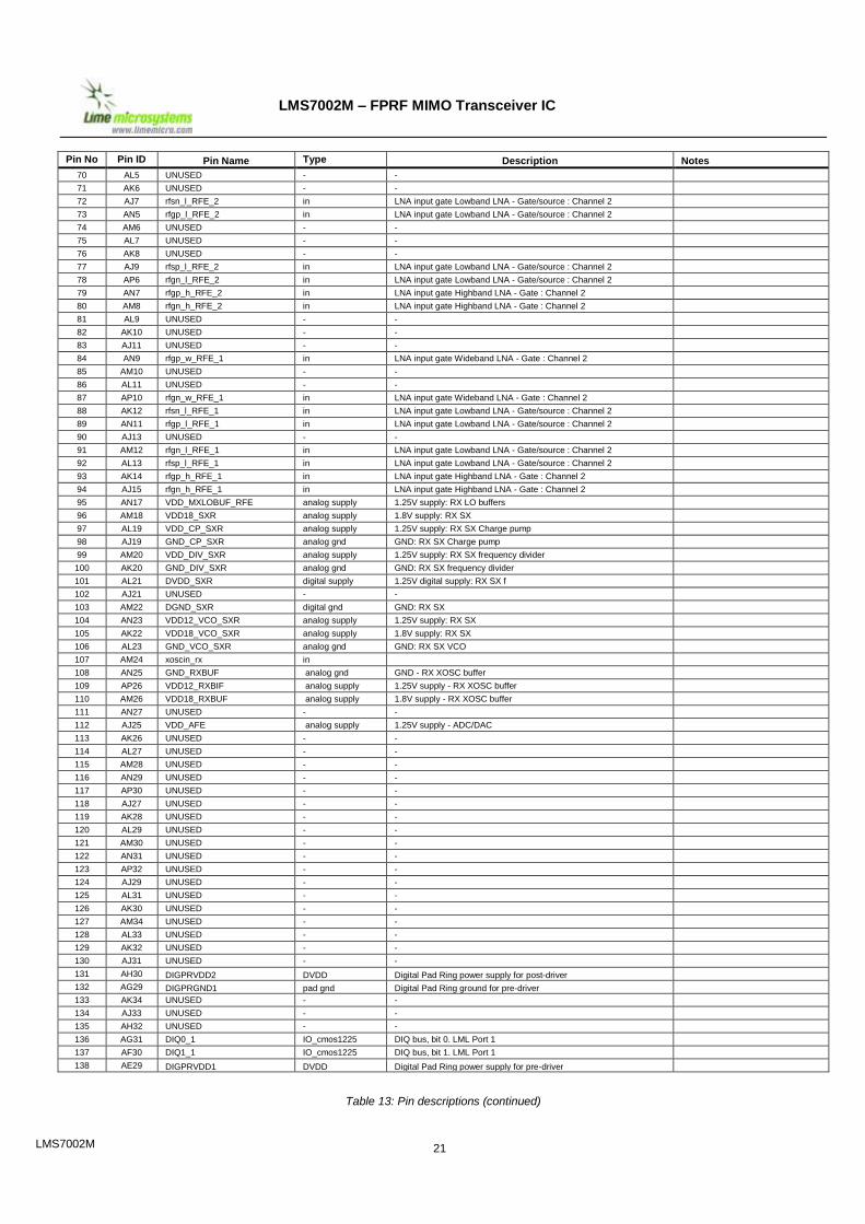
70 AL5 UNUSED - -
71 AK6 UNUSED - -
72 AJ7 rfsn_l_RFE_2 in LNA input gate Lowband LNA - Gate/source : Channel 2
73 AN5 rfgp_l_RFE_2 in LNA input gate Lowband LNA - Gate/source : Channel 2
74 AM6 UNUSED - -
75 AL7 UNUSED - -
76 AK8 UNUSED - -
77 AJ9 rfsp_l_RFE_2 in LNA input gate Lowband LNA - Gate/source : Channel 2
78 AP6 rfgn_l_RFE_2 in LNA input gate Lowband LNA - Gate/source : Channel 2
79 AN7 rfgp_h_RFE_2 in LNA input gate Highband LNA - Gate : Channel 2
80 AM8 rfgn_h_RFE_2 in LNA input gate Highband LNA - Gate : Channel 2
81 AL9 UNUSED - -
82 AK10 UNUSED - -
83 AJ11 UNUSED - -
84 AN9 rfgp_w_RFE_1 in LNA input gate Wideband LNA - Gate : Channel 2
85 AM10 UNUSED - -
86 AL11 UNUSED - -
87 AP10 rfgn_w_RFE_1 in LNA input gate Wideband LNA - Gate : Channel 2
88 AK12 rfsn_l_RFE_1 in LNA input gate Lowband LNA - Gate/source : Channel 2
89 AN11 rfgp_l_RFE_1 in LNA input gate Lowband LNA - Gate/source : Channel 2
90 AJ13 UNUSED - -
91 AM12 rfgn_l_RFE_1 in LNA input gate Lowband LNA - Gate/source : Channel 2
92 AL13 rfsp_l_RFE_1 in LNA input gate Lowband LNA - Gate/source : Channel 2
93 AK14 rfgp_h_RFE_1 in LNA input gate Highband LNA - Gate : Channel 2
94 AJ15 rfgn_h_RFE_1 in LNA input gate Highband LNA - Gate : Channel 2
95 AN17 VDD_MXLOBUF_RFE analog supply 1.25V supply: RX LO buffers
96 AM18 VDD18_SXR analog supply 1.8V supply: RX SX
97 AL19 VDD_CP_SXR analog supply 1.25V supply: RX SX Charge pump
98 AJ19 GND_CP_SXR analog gnd GND: RX SX Charge pump
99 AM20 VDD_DIV_SXR analog supply 1.25V supply: RX SX frequency divider
100 AK20 GND_DIV_SXR analog gnd GND: RX SX frequency divider
101 AL21 DVDD_SXR digital supply 1.25V digital supply: RX SX f
102 AJ21 UNUSED - -
103 AM22 DGND_SXR digital gnd GND: RX SX
104 AN23 VDD12_VCO_SXR analog supply 1.25V supply: RX SX
105 AK22 VDD18_VCO_SXR analog supply 1.8V supply: RX SX
106 AL23 GND_VCO_SXR analog gnd GND: RX SX VCO
107 AM24 xoscin_rx in
108 AN25 GND_RXBUF analog gnd GND - RX XOSC buffer
109 AP26 VDD12_RXBIF analog supply 1.25V supply - RX XOSC buffer
110 AM26 VDD18_RXBUF analog supply 1.8V supply - RX XOSC buffer
111 AN27 UNUSED - -
112 AJ25 VDD_AFE analog supply 1.25V supply - ADC/DAC
113 AK26 UNUSED - -
114 AL27 UNUSED - -
115 AM28 UNUSED - -
116 AN29 UNUSED - -
117 AP30 UNUSED - -
118 AJ27 UNUSED - -
119 AK28 UNUSED - -
120 AL29 UNUSED - -
121 AM30 UNUSED - -
122 AN31 UNUSED - -
123 AP32 UNUSED - -
124 AJ29 UNUSED - -
125 AL31 UNUSED - -
126 AK30 UNUSED - -
127 AM34 UNUSED - -
128 AL33 UNUSED - -
129 AK32 UNUSED - -
130 AJ31 UNUSED - -
131 AH30 DIGPRVDD2 DVDD Digital Pad Ring power supply for post-driver
132 AG29 DIGPRGND1 pad gnd Digital Pad Ring ground for pre-driver
133 AK34 UNUSED - -
134 AJ33 UNUSED - -
135 AH32 UNUSED - -
136 AG31 DIQ0_1 IO_cmos1225 DIQ bus, bit 0. LML Port 1
137 AF30 DIQ1_1 IO_cmos1225 DIQ bus, bit 1. LML Port 1
138 AE29 DIGPRVDD1 DVDD Digital Pad Ring power supply for pre-driver
Table 13: Pin descriptions (continued)
LMS7002M 22
LMS7002M – FPRF MIMO Transceiver IC
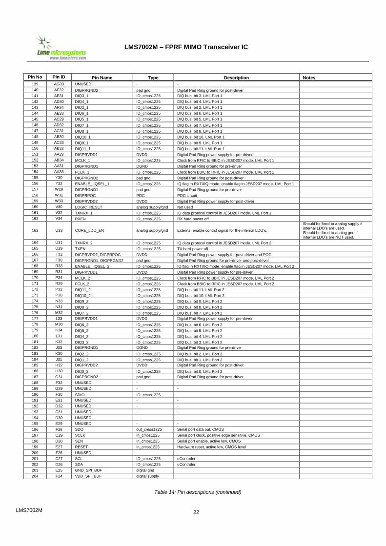
Pin No Pin ID Pin Name Type Description Notes
139 AG33 UNUSED - -
140 AF32 DIGPRGND2 pad gnd Digital Pad Ring ground for post-driver
141 AE31 DIQ3_1 IO_cmos1225 DIQ bus, bit 3. LML Port 1
142 AD30 DIQ4_1 IO_cmos1225 DIQ bus, bit 4. LML Port 1
143 AF34 DIQ2_1 IO_cmos1225 DIQ bus, bit 2. LML Port 1
144 AE33 DIQ6_1 IO_cmos1225 DIQ bus, bit 6. LML Port 1
145 AC29 DIQ5_1 IO_cmos1225 DIQ bus, bit 5. LML Port 1
146 AD32 DIQ7_1 IO_cmos1225 DIQ bus, bit 7. LML Port 1
147 AC31 DIQ8_1 IO_cmos1225 DIQ bus, bit 8. LML Port 1
148 AB30 DIQ10_1 IO_cmos1225 DIQ bus, bit 10. LML Port 1
149 AC33 DIQ9_1 IO_cmos1225 DIQ bus, bit 9. LML Port 1
150 AB32 DIQ11_1 IO_cmos1225 DIQ bus, bit 11. LML Port 1
151 AA29 DIGPRVDD1 DVDD Digital Pad Ring power supply for pre-driver
152 AB34 MCLK_1 IO_cmos1225 Clock from RFIC to BBIC in JESD207 mode. LML Port 1
153 AA31 DIGPRGND1 DGND Digital Pad Ring ground for pre-driver
154 AA33 FCLK_1 IO_cmos1225 Clock from BBIC to RFIC in JESD207 mode. LML Port 1
155 Y30 DIGPRGND2 pad gnd Digital Pad Ring ground for post-driver
156 Y32 ENABLE_ IQSEL_1 IO_cmos1225 IQ flag in RXTXIQ mode; enable flag in JESD207 mode. LML Port 1
157 W29 DIGPRGND1 pad gnd Digital Pad Ring ground for pre-driver
158 W31 DIGPRPOC POC POC circuit
159 W33 DIGPRVDD2 DVDD Digital Pad Ring power supply for post-driver
160 V30 LOGIC_RESET analog supply/gnd Not used
161 V32 TXNRX_1 IO_cmos1225 IQ data protocol control in JESD207 mode. LML Port 1
162 V34 RXEN IO_cmos1225 RX hard power off
163 U33 CORE_LDO_EN analog supply/gnd External enable control signal for the internal LDO’s.
Should be fixed to analog supply if internal LDO’s are used. Should be fixed to analog gnd if internal LDO’s are NOT used.
164 U31 TXNRX_2 IO_cmos1225 IQ data protocol control in JESD207 mode. LML Port 2
165 U29 TXEN IO_cmos1225 TX hard power off
166 T32 DIGPRVDD2, DIGPRPOC DVDD Digital Pad Ring power supply for post-driver and POC
167 T30 DIGPRGND1, DIGPRGND2 pad gnd Digital Pad Ring ground for pre-driver and post-driver
168 R33 ENABLE_ IQSEL_2 IO_cmos1225 IQ flag in RXTXIQ mode; enable flag in JESD207 mode. LML Port 2
169 R31 DIGPRVDD1 DVDD Digital Pad Ring power supply for pre-driver
170 P34 MCLK_2 IO_cmos1225 Clock from RFIC to BBIC in JESD207 mode. LML Port 2
171 R29 FCLK_2 IO_cmos1225 Clock from BBIC to RFIC in JESD207 mode. LML Port 2
172 P32 DIQ11_2 IO_cmos1225 DIQ bus, bit 11. LML Port 2
173 P30 DIQ10_2 IO_cmos1225 DIQ bus, bit 10. LML Port 2
174 N33 DIQ9_2 IO_cmos1225 DIQ bus, bit 9. LML Port 2
175 N31 DIQ8_2 IO_cmos1225 DIQ bus, bit 8. LML Port 2
176 M32 DIQ7_2 IO_cmos1225 DIQ bus, bit 7. LML Port 2
177 L33 DIGPRVDD1 DVDD Digital Pad Ring power supply for pre-driver
178 M30 DIQ6_2 IO_cmos1225 DIQ bus, bit 6. LML Port 2
179 K34 DIQ5_2 IO_cmos1225 DIQ bus, bit 5. LML Port 2
180 L31 DIQ4_2 IO_cmos1225 DIQ bus, bit 4. LML Port 2
181 K32 DIQ3_2 IO_cmos1225 DIQ bus, bit 3. LML Port 2
182 J33 DIGPRGND1 DGND Digital Pad Ring ground for pre-driver
183 K30 DIQ2_2 IO_cmos1225 DIQ bus, bit 2. LML Port 2
184 J31 DIQ1_2 IO_cmos1225 DIQ bus, bit 1. LML Port 2
185 H32 DIGPRVDD2 DVDD Digital Pad Ring ground for post-driver
186 H30 DIQ0_2 IO_cmos1225 DIQ bus, bit 0. LML Port 2
187 G31 DIGPRGND2 pad gnd Digital Pad Ring ground for post-driver
188 F32 UNUSED - -
189 G29 UNUSED - -
190 F30 SDIO IO_cmos1225
191 E31 UNUSED - -
192 D32 UNUSED - -
193 C31 UNUSED - -
194 D30 UNUSED - -
195 E29 UNUSED - -
196 F28 SDO out_cmos1225 Serial port data out, CMOS
197 C29 SCLK in_cmos1225 Serial port clock, positive edge sensitive, CMOS
198 D28 SEN in_cmos1225 Serial port enable, active low, CMOS
199 E27 RESET in_cmos1225 Hardware reset, active low, CMOS level
200 F26 UNUSED - -
201 C27 SCL IO_cmos1225 uControler
202 D26 SDA IO_cmos1225 uControler
203 E25 GND_SPI_BUF digital gnd
204 F24 VDD_SPI_BUF digital supply
Table 14: Pin descriptions (continued)
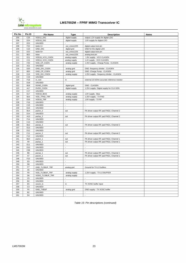
LMS7002M 23
LMS7002M – FPRF MIMO Transceiver IC
Pin No Pin ID Pin Name Type Description Notes
205 C25 VDD12_DIG digital supply output 1.2V supply for digital LDO
206 D24 VDD18_DIG digital supply 1.8V supply for digital LDO
207 E23 UNUSED - -
208 F22 tstdo<1> out_cmos1225 digital output test pin
209 C23 GND_DIG digital gnd GND for the digital LDO
210 D22 tstdo<0> out_cmos1225 digital output test pin
211 B22 tstao out_cmos1225 analog test pin
212 E21 VDD18_VCO_CGEN analog supply 1.8V supply - VCO CLKGEN
213 C21 VDD14_VCO_CGEN analog supply 1.4V supply - VCO CLKGEN
214 F20 VDD_CP_CGEN analog supply 1.25V supply - Charge Pump - CLKGEN
215 A21 UNUSED - -
216 D20 GND_DIV_CGEN analog gnd GND -frequency divider - CLKGEN
217 B20 GND_CP_CGEN analog gnd GND -Charge Pump - CLKGEN
218 E19 VDD_DIV_CGEN analog supply 1.25V supply - frequency divider - CLKGEN
219 C19 UNUSED - -
220 F18 vr_rext in external 10 kOhm accurate reference resistor
221 D18 UNUSED - -
222 B18 DGND_CGEN digital gnd GND - CLKGEN
223 A17 DVDD_CGEN digital supply 1.25V supply- Digital supply for CLK GEN
224 C17 UNUSED - -
225 E17 VDD18_BIAS analog supply 1.8V supply - Bias
226 B16 VDD_TPAD_TRF analog supply 1.25V supply - TX PAD
227 D16 VDD18_TRF analog supply 1.8V supply - TX RF
228 F16 UNUSED - -
229 C15 UNUSED - -
230 E15 UNUSED - -
231 B14 pa2on_2 out PA driver output RF pad PAD2, Channel 2
232 D14 UNUSED - -
233 A13 pa2op_2 out PA driver output RF pad PAD2, Channel 2
234 F14 UNUSED - -
235 C13 UNUSED - -
236 B12 pa1op_2 out PA driver output RF pad PAD1, Channel 2
237 E13 UNUSED - -
238 D12 UNUSED - -
239 C11 pa1on_2 out PA driver output RF pad PAD1, Channel 2
240 F12 UNUSED - -
241 B10 pa2on_1 out PA driver output RF pad PAD2, Channel 1
242 A9 pa2op_1 out PA driver output RF pad PAD2, Channel 1
243 E11 UNUSED - -
244 D10 UNUSED - -
245 C99 UNUSED - -
246 B8 pa1op_1 out PA driver output RF pad PAD1, Channel 1
247 A7 pa1on_1 out PA driver output RF pad PAD1, Channel 1
248 F10 UNUSED - -
249 E9 UNUSED - -
250 D8 UNUSED - -
251 C7 GND_TLOBUF_TRF analog gnd Ground for TX LO buffers
252 A5 UNUSED - -
253 F8 VDD_TLOBUF_TRF analog supply 1.25V supply - TX LO BUFFER
254 D6 VDDO_TLOBUF_TRF analog supply
255 C5 UNUSED - -
256 B4 UNUSED - -
257 E5 xoscin_tx in TX XOSC buffer input
258 C3 UNUSED - -
259 F6 GND_TXBUF analog gnd GND supply - TX XOSC buffer
260 B2 UNUSED - -
261 D4 UNUSED - -
Table 15: Pin descriptions (continued)
LMS7002M 24
LMS7002M – FPRF MIMO Transceiver IC
TYPICAL APPLICATION
A typical application circuit of the LMS7002M is given in Figure 51. Note that only the RF part of a single MIMO TRX chain is shown. More details can be found in the LMS7002M evaluation board schematics.
Figure 51: Typical application circuit
Lime Microsystems Surrey Technology Centre Occam Road The Surrey Research Park Guildford GU2 7YG, Surrey United Kingdom
Tel: +44 (0) 1483 685 063 e-mail: [email protected] http://www.limemicro.com
ORDERING INFORMATION
Model Temperature Range Package Description
LMS7002M -40oC to +85
oC 261 pin aQFN
LMS7002M-REEL -40oC to +85
oC 261 pin aQFN
LMS7002M-EVB Evaluation board
REVISION HISTORY
The following table shows the revision history of this document:
Date Version Description of Revisions
05/11/2013 2.0.0 Major update.
02/07/2014 2.1.0 Performance parameters corrections based on measurement data.
10/09/2014 2.2.0 Performance parameters corrections based on measurement data.
NOTICE OF DISCLAMER
The information disclosed to you hereunder (the “Materials”) is provided solely for the selection and use of Lime Microsystems products. To the maximum extent permitted by applicable law: (1) Materials are made available “AS IS” and with all faults, Lime Microsystems hereby DISCLAIMS ALL WARRANTIES AND CONDITIONS, EXPRESS, IMPLIED, OR STATUTORY, INCLUDING BUT NOT LIMITED TO WARRRANTIES OF MERCHANTABILITY, NON-INFRIGEMENT, OR FITNESS FOR ANY PARTICULAR PURPOSE; and (2) Lime Microsystems shall not be liable (whether in contract or tort, including negligence, or under any other theory of liability) for any loss or damage of any kind or nature related to, arising under, or in connection with, the Materials (including your use of the Materials), including for any direct, indirect, special, incidental, or consequential loss or damage (including loss of data, profits, goodwill, or any type of loss or damage suffered as a result of any action brought by a third party) even if such damage or loss was reasonably foreseeable or Lime Microsystems had been advised of the possibility of the same. Lime Microsystems assumes no obligation to correct any errors contained in the Materials, or to advise you of any corrections or update. You may not reproduce, modify, distribute, or publicly display the Materials without prior written consent. Certain products are subject to the terms and conditions of the Limited Warranties. Lime Microsystems products are not designed or intended to be fail-safe or for use in any application requiring fail-safe performance; you assume sole risk and liability for use of Lime Microsystems products in Critical Applications.