Embed Size (px)
Citation preview
10/10/2005 Applying a Drain Voltage to an NMOS Device 1/10
Jim Stiles The Univ. of Kansas Dept. of EECS
Applying a Drain Voltage to an NMOS Device
Say we apply a voltage at the gate of an NMOS device that is sufficiently large to induce a conducting channel (i.e.,
0GS tv V− > ). Now, say that we additionally place a voltage at the NMOS drain electrode, such that:
0DSv > where:
Drain-to-Source VoltageSDS Dv v v= −
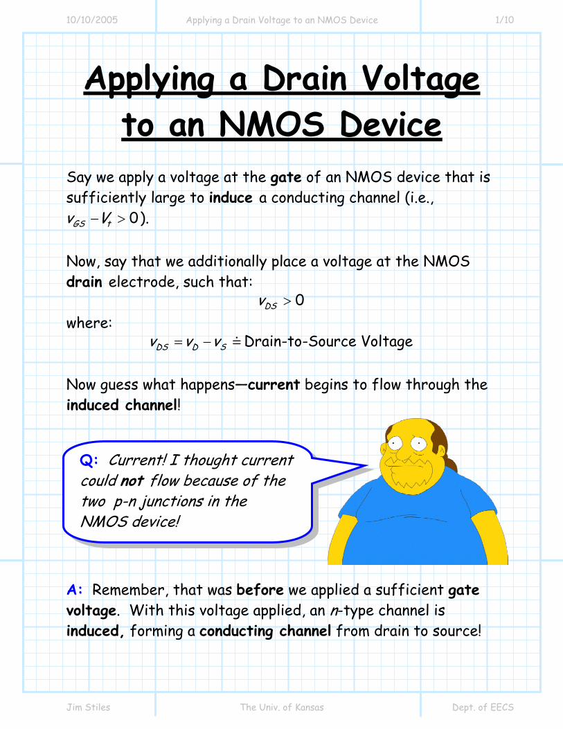
Now guess what happens—current begins to flow through the induced channel! A: Remember, that was before we applied a sufficient gate voltage. With this voltage applied, an n-type channel is induced, forming a conducting channel from drain to source!
Q: Current! I thought current could not flow because of the two p-n junctions in the NMOS device!
10/10/2005 Applying a Drain Voltage to an NMOS Device 2/10
Jim Stiles The Univ. of Kansas Dept. of EECS
Recall that because of the SiO2 layer, the gate current is zero (i.e., 0Gi = ). Thus, all current entering the drain will exit the source. We therefore conclude that:
S Di i= As a result, we refer to the channel current for NMOS devices as simply the drain current iD.
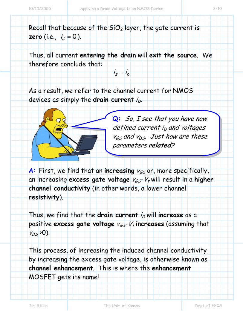
A: First, we find that an increasing vGS or, more specifically, an increasing excess gate voltage vGS-Vt will result in a higher channel conductivity (in other words, a lower channel resistivity). Thus, we find that the drain current iD will increase as a positive excess gate voltage vGS-Vt increases (assuming that vDS >0). This process, of increasing the induced channel conductivity by increasing the excess gate voltage, is otherwise known as channel enhancement. This is where the enhancement MOSFET gets its name!
Q: So, I see that you have now defined current iD and voltages vGS and vDS. Just how are these parameters related?

10/10/2005 Applying a Drain Voltage to an NMOS Device 3/10
Jim Stiles The Univ. of Kansas Dept. of EECS
A: This relationship is a little complicated! Generally speaking, however, a positive vDS results in a positive iD, and the larger the vDS, the larger the drain current iD. More specifically, we find that when vDS is small (we’ll see how small later), the drain current will be directly proportional to the voltage drain to source vDS.
DS v smallD DSi v∝ if In other words, if vDS is zero, the drain current iD is zero. Or, if the voltage vDS increases by 10%, the drain current will likewise increase by 10%. Note this is just like a resistor!
vi i vR
= ∴ ∝
Thus, if (and only if!) vDS is small, the induced channel behaves like a resistor—the current through the channel (iD) is directly proportional to the voltage across it (vDS).
Q: OK, but what about the relationship between drain current iD and voltage vDS?
vDS
iD
10/10/2005 Applying a Drain Voltage to an NMOS Device 4/10
Jim Stiles The Univ. of Kansas Dept. of EECS
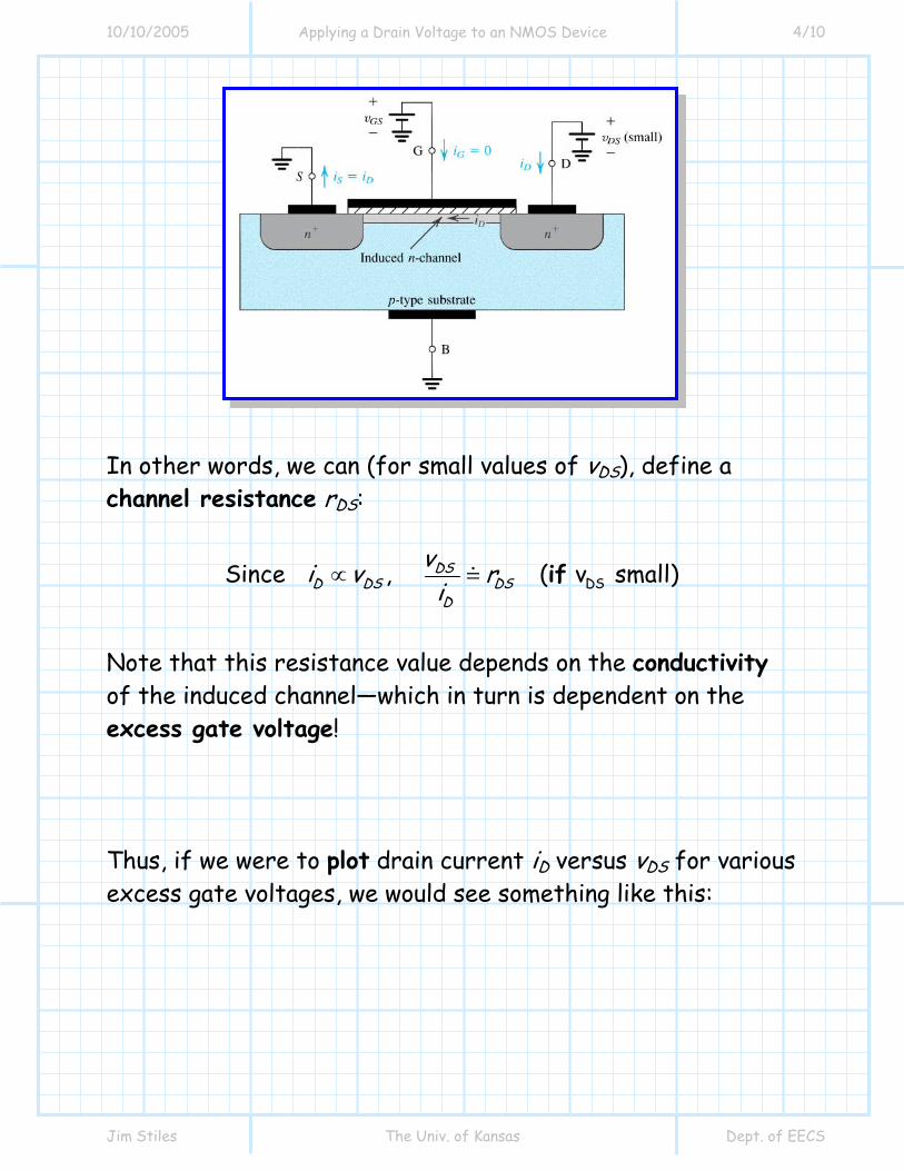
In other words, we can (for small values of vDS), define a channel resistance rDS:
DSSince , ( v small) DS
D DS DSD
vi v ri
∝ if
Note that this resistance value depends on the conductivity of the induced channel—which in turn is dependent on the excess gate voltage!
Thus, if we were to plot drain current iD versus vDS for various excess gate voltages, we would see something like this:
10/10/2005 Applying a Drain Voltage to an NMOS Device 5/10
Jim Stiles The Univ. of Kansas Dept. of EECS
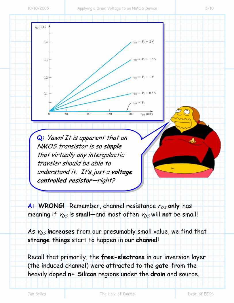
A: WRONG! Remember, channel resistance rDS only has meaning if vDS is small—and most often vDS will not be small! As vDS increases from our presumably small value, we find that strange things start to happen in our channel! Recall that primarily, the free-electrons in our inversion layer (the induced channel) were attracted to the gate from the heavily doped n+ Silicon regions under the drain and source.
Q: Yawn! It is apparent that an NMOS transistor is so simple that virtually any intergalactic traveler should be able to understand it. It’s just a voltage controlled resistor—right?

10/10/2005 Applying a Drain Voltage to an NMOS Device 6/10
Jim Stiles The Univ. of Kansas Dept. of EECS
But the gate now has competition in attracting these free electrons! It was “easy” to attract free electrons to the gate when the gate electrode voltage was much larger than both the drain and source voltage (i.e., when GS DSv v ). But as the drain voltage increases, it begins to attract free electrons of its own! Recall that positive current entering the drain will actually consist mainly of free electrons exiting the drain! As a result, the concentration of free-electrons in our inversion layer will begin to decrease in the vicinity of the drain. In other words, increasing vDS will result in decreasing channel conductivity!

10/10/2005 Applying a Drain Voltage to an NMOS Device 7/10
Jim Stiles The Univ. of Kansas Dept. of EECS
Thus, increasing the vDS will have two effects on the NMOS device:
1. Increasing vDS will increase the potential difference (voltage) across the conducting channel, an effect that works to increase the drain current iD
2. Increasing vDS will decrease the conductivity of the
induced channel, and effect that works to decrease the drain current iD.
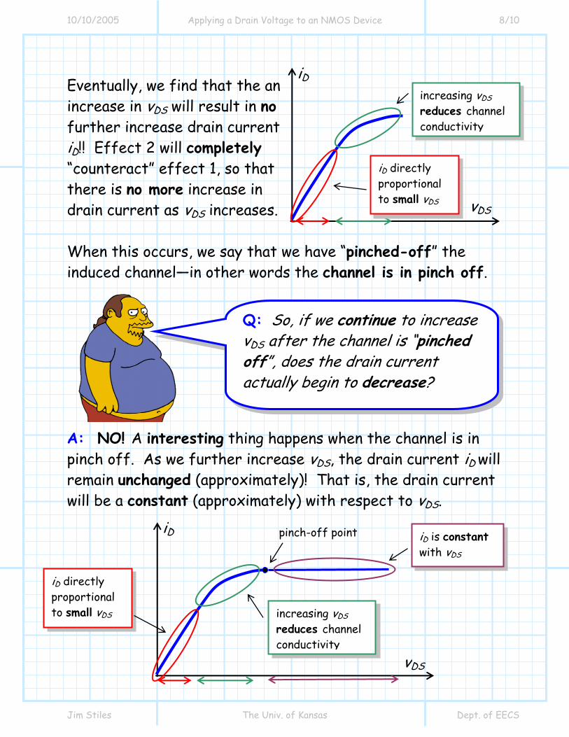
For small values of vDS, the second effect is tiny, so that the increase in drain current is directly proportional to the increase in voltage vDS (hence, we can define channel resistance rDS). For example, a 10% increase in vDS will result in a 10% increase in drain current. However, as vDS increases, the second effect will become more and more pronounced. We find then that the drain current will no longer be directly proportional to the voltage vDS. The reduction in channel conductivity will begin to “counteract” the increase in potential across the channel. For example, a 10% increase in vDS may result in only a 9% increase in iD. Likewise, if we increase vDS another 10%, the drain current may then increase only 8% (and so on).
vDS
iD iD directly proportional to small vDS
10/10/2005 Applying a Drain Voltage to an NMOS Device 8/10
Jim Stiles The Univ. of Kansas Dept. of EECS
Eventually, we find that the an increase in vDS will result in no further increase drain current iD!! Effect 2 will completely “counteract” effect 1, so that there is no more increase in drain current as vDS increases. When this occurs, we say that we have “pinched-off” the induced channel—in other words the channel is in pinch off. A: NO! A interesting thing happens when the channel is in pinch off. As we further increase vDS, the drain current iD will remain unchanged (approximately)! That is, the drain current will be a constant (approximately) with respect to vDS.
Q: So, if we continue to increase vDS after the channel is “pinched off”, does the drain current actually begin to decrease?
vDS
iD pinch-off point iD is constant with vDS
increasing vDS reduces channel conductivity
iD directly proportional to small vDS
vDS
iD increasing vDS reduces channel conductivity
iD directly proportional to small vDS
10/10/2005 Applying a Drain Voltage to an NMOS Device 9/10
Jim Stiles The Univ. of Kansas Dept. of EECS
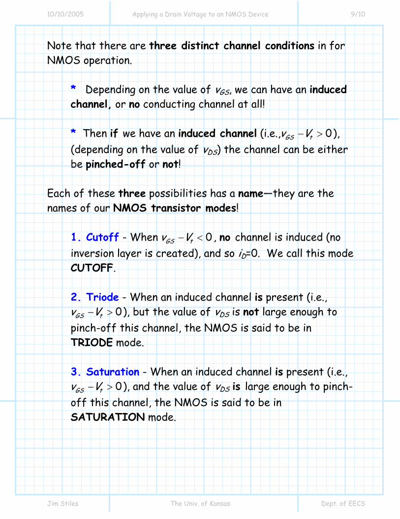
Note that there are three distinct channel conditions in for NMOS operation.
* Depending on the value of vGS, we can have an induced channel, or no conducting channel at all!
* Then if we have an induced channel (i.e., 0GS tv V− > ), (depending on the value of vDS) the channel can be either be pinched-off or not!
Each of these three possibilities has a name—they are the names of our NMOS transistor modes!
1. Cutoff - When 0GS tv V− < , no channel is induced (no inversion layer is created), and so iD=0. We call this mode CUTOFF. 2. Triode - When an induced channel is present (i.e.,
0GS tv V− > ), but the value of vDS is not large enough to pinch-off this channel, the NMOS is said to be in TRIODE mode. 3. Saturation - When an induced channel is present (i.e.,
0GS tv V− > ), and the value of vDS is large enough to pinch-off this channel, the NMOS is said to be in SATURATION mode.
10/10/2005 Applying a Drain Voltage to an NMOS Device 10/10
Jim Stiles The Univ. of Kansas Dept. of EECS
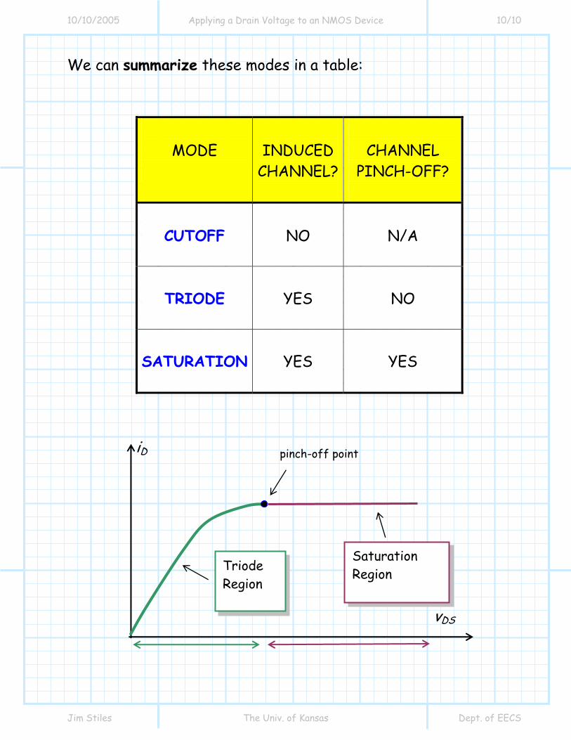
We can summarize these modes in a table:
MODE
INDUCED
CHANNEL?
CHANNEL
PINCH-OFF?
CUTOFF
NO
N/A
TRIODE
YES
NO
SATURATION
YES
YES
vDS
iD pinch-off point
Saturation Region Triode
Region