Embed Size (px)
Citation preview
ARTICLE IN PRESS
Nuclear Instruments and Methods in Physics Research A 520 (2004) 424–426
*Corresp
E-mail a
(M.J. Myer
0168-9002/$
doi:10.1016
Arrays of antenna-coupled bolometers using transitionedge sensors
Michael J. Myersa,*, William Holzapfela, Adrian T. Leea, Roger O’Brienta,P.L. Richardsa, D. Schwana, A.D. Smithb, Helmuth Spielerc, Huan Trana
aPhysics Department, University of California, Berkeley, CA 94720, USAbTRW Inc., Redondo Beach, CA 90278, USA
cPhysics Division, Lawrence Berkeley National Laboratory, Berkeley, CA 94720, USA
Abstract
We are developing antenna-coupled transition edge sensor (TES) bolometer arrays for use in the measurement of the
cosmic microwave background polarization. We have designed and built a prototype antenna-coupled bolometer pixel.
This design uses a double slot dipole antenna on a silicon hemispherical lens, fed with superconducting niobium
microstrip. Microstrip filters are used to define the frequency band of the optical response, which is centered at 217GHz
with 40% bandwidth. The microstrip is terminated into a load resistor on a silicon nitride suspension, adjacent to a TES
which is used to measure the dissipated power.
We will discuss our progress in the development of the prototype pixel chips as well as the baseline design of a
bolometer array for POLARBEAR, a CMB polarization experiment.
r 2003 Elsevier B.V. All rights reserved.
PACS: 85.25.Pb; 07.57.Kp; 85.60.Gz
Keywords: Bolometer; Antenna-coupled; Transition edge sensor
1. Introduction
Recent experiments using bolometers to studythe anisotropy of the cosmic microwave back-ground (CMB) have yielded significant insight intothe early evolution of the universe. Characteriza-tion of the CMB polarization promises to furtherbroaden our understanding of this era. Today’sbolometers are typically near the photon noiselimit in these regimes, so large bolometer arrays
onding author. Tel.: +1-510-642-4359.
ddress: [email protected]
s).
- see front matter r 2003 Elsevier B.V. All rights reserve
/j.nima.2003.11.351
are needed to continue to improve the sensitivityof future observations.Antenna-coupled bolometers using transition
edge sensors (TESs) are well suited to large arrayconstruction. We have designed and built aprototype single pixel antenna-coupled detector.We have also begun design on a detector arraybased on the prototype pixel.
2. Single pixel design and construction
Our prototype design uses a dual-slot dipoleplanar antenna. This antenna has a symmetric
d.
ARTICLE IN PRESS
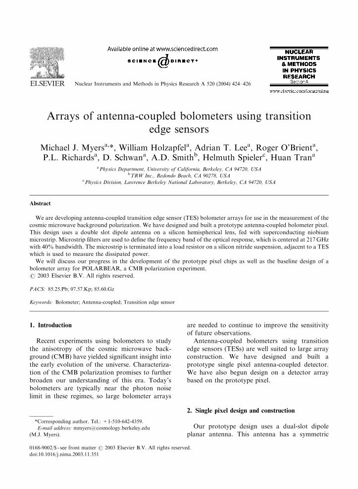
Fig. 1. Photograph of two antennas on a prototype test chip
and band defining filters for one of them. The antenna on the
left is the dual polarization variant.
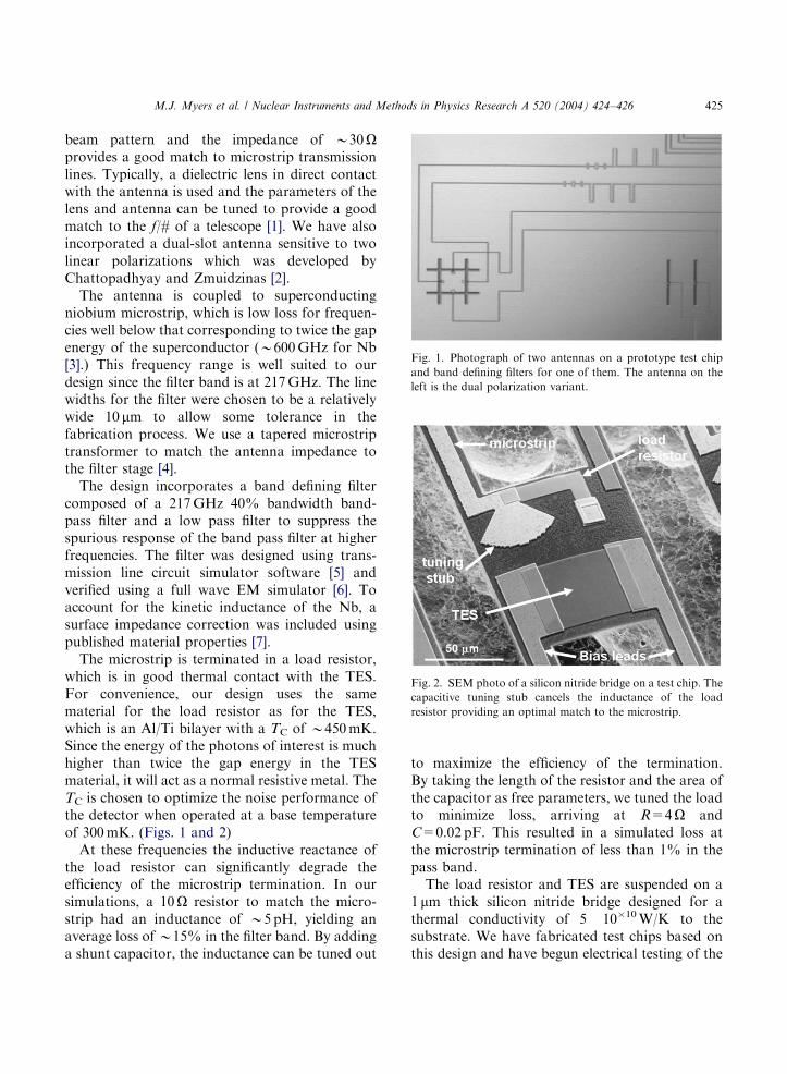
Fig. 2. SEM photo of a silicon nitride bridge on a test chip. The
capacitive tuning stub cancels the inductance of the load
resistor providing an optimal match to the microstrip.
M.J. Myers et al. / Nuclear Instruments and Methods in Physics Research A 520 (2004) 424–426 425
beam pattern and the impedance of B30Oprovides a good match to microstrip transmissionlines. Typically, a dielectric lens in direct contactwith the antenna is used and the parameters of thelens and antenna can be tuned to provide a goodmatch to the f/# of a telescope [1]. We have alsoincorporated a dual-slot antenna sensitive to twolinear polarizations which was developed byChattopadhyay and Zmuidzinas [2].The antenna is coupled to superconducting
niobium microstrip, which is low loss for frequen-cies well below that corresponding to twice the gapenergy of the superconductor (B600GHz for Nb[3].) This frequency range is well suited to ourdesign since the filter band is at 217GHz. The linewidths for the filter were chosen to be a relativelywide 10 mm to allow some tolerance in thefabrication process. We use a tapered microstriptransformer to match the antenna impedance tothe filter stage [4].The design incorporates a band defining filter
composed of a 217GHz 40% bandwidth band-pass filter and a low pass filter to suppress thespurious response of the band pass filter at higherfrequencies. The filter was designed using trans-mission line circuit simulator software [5] andverified using a full wave EM simulator [6]. Toaccount for the kinetic inductance of the Nb, asurface impedance correction was included usingpublished material properties [7].The microstrip is terminated in a load resistor,
which is in good thermal contact with the TES.For convenience, our design uses the samematerial for the load resistor as for the TES,which is an Al/Ti bilayer with a TC of B450mK.Since the energy of the photons of interest is muchhigher than twice the gap energy in the TESmaterial, it will act as a normal resistive metal. TheTC is chosen to optimize the noise performance ofthe detector when operated at a base temperatureof 300mK. (Figs. 1 and 2)At these frequencies the inductive reactance of
the load resistor can significantly degrade theefficiency of the microstrip termination. In oursimulations, a 10O resistor to match the micro-strip had an inductance of B5 pH, yielding anaverage loss ofB15% in the filter band. By addinga shunt capacitor, the inductance can be tuned out
to maximize the efficiency of the termination.By taking the length of the resistor and the area ofthe capacitor as free parameters, we tuned the loadto minimize loss, arriving at R=4O andC=0.02 pF. This resulted in a simulated loss atthe microstrip termination of less than 1% in thepass band.The load resistor and TES are suspended on a
1 mm thick silicon nitride bridge designed for athermal conductivity of 5� 10�10W/K to thesubstrate. We have fabricated test chips based onthis design and have begun electrical testing of the

ARTICLE IN PRESS
M.J. Myers et al. / Nuclear Instruments and Methods in Physics Research A 520 (2004) 424–426426
single pixel devices. Optical testing will followshortly.
3. Array design
Antenna-coupled bolometers using TESs areparticularly well suited to large array construction.The planar antennas provide directivity andremove the need for a horn antenna per pixel.Transmission line filters remove the need for manyof the bulky filters often used to define the passband of each pixel. The SQUID readout used withTESs is amenable to multiplexing schemes, andSQUID multiplexers are currently under develop-ment by several groups.The double slot dipole antenna used in our
single pixel design typically requires a silicon lensto couple the antenna efficiently to a telescope.This presents a challenge for array construction.One option is to use a lens per antenna. This lensarray would resemble a fly’s eye and has beendescribed in detail by Buttgenbach [8]. Otheroptions exist, such as the use of a reflector behinda membrane mounted antenna [9].We are currently designing an antenna-coupled
bolometer array based on our prototype pixel andusing a silicon lens for each antenna. The array isintended for use in the first stage of the CMBpolarization experiment POLARBEAR. The dou-ble slot dipole antenna/silicon lens combination iswell understood and proven. It also provides asignificant amount of space around each antenna,so that the RF filters and TESs can be placed nextto their respective antennas. This keeps themicrostrip feeding the antenna short, so that theeffect of loss in the microstrip is minimized.Construction of the lens array is being investigatedand we have built an array of 1000 mock lensesusing a machined jig. The required precision of the
alignment is within standard machining tolerancesand silicon hemispheres are available commer-cially for several dollars each.
4. Conclusion
We have designed and fabricated single pixelantenna-coupled bolometers with transition edgesensors and begun testing them. We are alsodesigning a detector array based on this pixel,which will be fabricated when operation of thesingle pixel design is verified.
Acknowledgements
This work was supported in part by NSF GrantFD97-31200. All devices were fabricated at the UCBerkeley Microfabrication Laboratory.
References
[1] D. Filipovic, S. Gearhart, G. Rebeiz, IEEE Trans. Micro-
wave Theory Tech. 41 (10) (1993) 1738.
[2] G. Chattopadhyay, J. Zmuidzinas, IEEE Trans. Antennas
Propog. 46 (5) (1998) 736.
[3] R.L. Kautz, J. Appl. Phys. 49 (1) (1978) 308.
[4] D. McGinnis, J. Beyer, IEEE Trans. Microwave Theory
Tech. 36 (11) (1988) 1521.
[5] MMICAD, Optotek LTD. http://www.optotek.com.
[6] Sonnet em Suite, Sonnet Software, Inc. http://www.
sonnetusa.com.
[7] A.R. Kerr, Surface impedance of superconductors and
normal conductors in EM simulators, ALMA Memo
No. 245, http://www.alma.nrao.edu/memos/html-memos/
alma245.1.pdf.
[8] T. Buttgenbach, IEEE Trans. Microwave Theory Tech. 41
(10) (1993) 760.
[9] D. Filipovic, W. Ali-Ahmad, G. Rebeiz, IEEE Trans.
Microwave Theory and Techniques 40 (5) (1992) 962.

![lezione11 2016 cos.ppt [modalità compatibilità]oberon.roma1.infn.it/lezioni/cosmologia...stack cold, stepping HWP polarizer arrays of multimode feedhorns and bolometers UHMWPE lens](https://img.pdfslide.net/doc/110x75/5eb5a06b084cac04e27ff393/lezione11-2016-cosppt-modalit-compatibilit-stack-cold-stepping-hwp-polarizer.jpg)


![Travelling waves in chains of pulse-coupled integrate-and …bresslof/publications/99-2.pdfrhythms [1,2], chemical oscillators [3], Josephson junction arrays [4,5] and laser arrays](https://img.pdfslide.net/doc/110x75/60f69f2c60224e083c5e9cc1/travelling-waves-in-chains-of-pulse-coupled-integrate-and-bresslofpublications99-2pdf.jpg)