Embed Size (px)
Citation preview
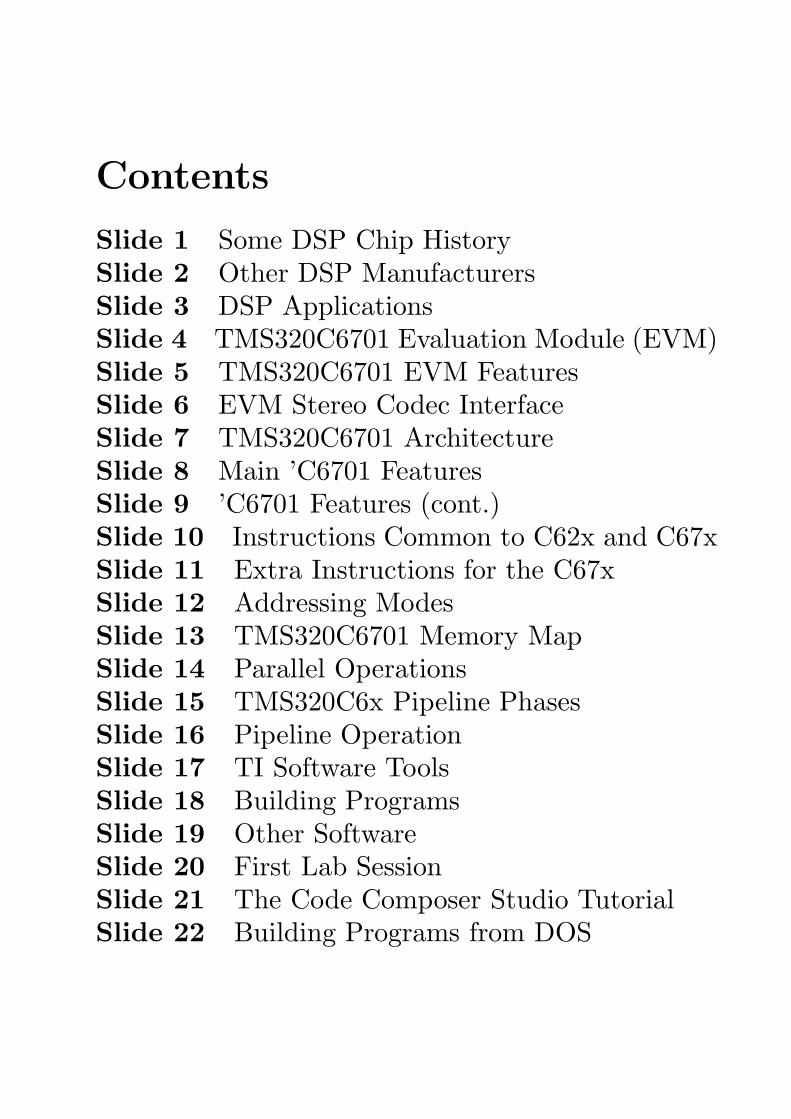
Contents
Slide 1 Some DSP Chip HistorySlide 2 Other DSP ManufacturersSlide 3 DSP ApplicationsSlide 4 TMS320C6701 Evaluation Module (EVM)Slide 5 TMS320C6701 EVM FeaturesSlide 6 EVM Stereo Codec InterfaceSlide 7 TMS320C6701 ArchitectureSlide 8 Main ’C6701 FeaturesSlide 9 ’C6701 Features (cont.)Slide 10 Instructions Common to C62x and C67xSlide 11 Extra Instructions for the C67xSlide 12 Addressing ModesSlide 13 TMS320C6701 Memory MapSlide 14 Parallel OperationsSlide 15 TMS320C6x Pipeline PhasesSlide 16 Pipeline OperationSlide 17 TI Software ToolsSlide 18 Building ProgramsSlide 19 Other SoftwareSlide 20 First Lab SessionSlide 21 The Code Composer Studio TutorialSlide 22 Building Programs from DOS
'
&
$
%
Some DSP Chip History
First Commercial DSP’s
• 1982 – NEC µPD7720
• 1982 – TMS 32010
These chips initially cost around $600. Now cost
less than $1.
Texas Instruments (TI) DSP Family
• Low Cost, Fixed-Point, 16-Bit Word length
Motor control, disk head positioning, control
TMS320C1x, ’C2x, ’C20x, ’C24x
• Power Efficient, Fixed-Point, 16-Bit Words
Wireless phones, modems, VoIP
’C5x, ’C54x, ’C55x
• High Performance DSP’s
Comm Infrastructure, xDSL, Imaging, Video
’C62x (16-bit fixed-point)
’C3x, ’C4x, ’C64x, ’C67x (32-bit
floating-point)
’C8x (multi-cpu)
1
'
&
$
%
Other DSP Manufacturers
Lucent, Motorola, Analog Devices, Rockwell,
Thomson, Fujitsu
Fixed vs. Floating-Point DSP’s
• Fixed-point DSP’s are cheaper and use less
power but care must be taken with scaling to
avoid over and underflow.
• Floating-point DSP’s are easier to program.
Numbers are automatically scaled. They are
more complicated and expensive.
Advantages of DSP’s over Analog Circuits
• Can implement complex linear or nonlinear
algorithms.
• Can modify easily by changing software.
• Reduced parts count makes fabrication easier.
• High reliability
2
'
&
$
%
DSP Applications
• Telecommunications: telephone line modems, FAX,
cellular telephones, speaker phones, answering
machines
• Voice/Speech: speech digitization and compression,
voice mail, speaker verification, and speech synthesis
• Automotive: engine control, antilock brakes, active
suspension, airbag control, and system diagnosis
• Control Systems: head positioning servo systems in
disk drives, laser printer control, robot control, engine
and motor control, and numerical control of automatic
machine tools
• Military: radar and sonar signal processing,
navigation systems, missile guidance, HF radio
frequency modems, secure spread spectrum radios, and
secure voice
• Medical: hearing aids, MRI imaging, ultrasound
imaging, and patient monitoring
• Instrumentation: spectrum analysis, transient
analysis, signal generators
• Image Processing: HDTV, image enhancement,
image compression and transmission, 3-D rotation,
and animation
3
'
&
$
%
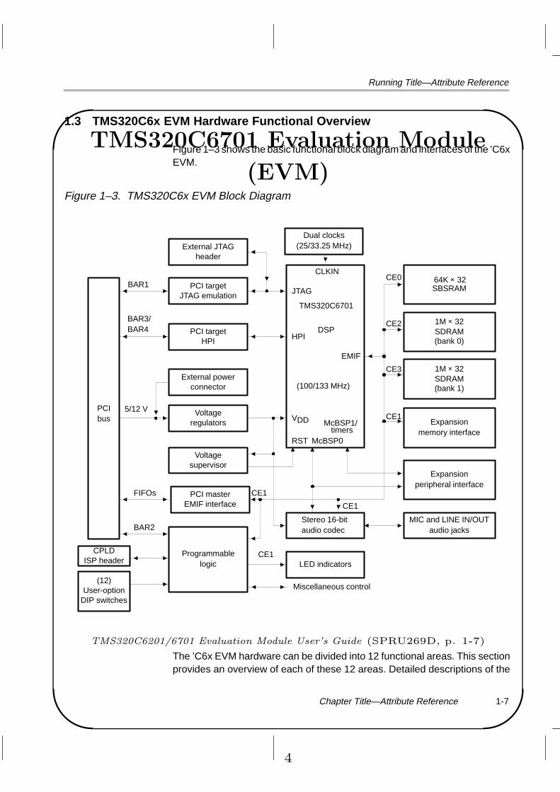
TMS320C6701 Evaluation Module
(EVM)
Running Title—Attribute Reference
1-7 Chapter Title—Attribute Reference
1.3 TMS320C6x EVM Hardware Functional Overview
Figure 1–3 shows the basic functional block diagram and interfaces of the ’C6xEVM.
Figure 1–3. TMS320C6x EVM Block Diagram
PCIbus
PCI targetJTAG emulation
PCI targetHPI
PCI masterEMIF interface
Dual clocks(25/33.25 MHz)External JTAG
header
Voltageregulators
Stereo 16-bitaudio codec
64K × 32SBSRAM
1M × 32SDRAM(bank 0)
Expansionmemory interface
Expansionperipheral interface
MIC and LINE IN/OUTaudio jacks
External powerconnector
Voltagesupervisor
JTAG
HPI
VDD
RST McBSP0
EMIF
CLKIN
TMS320C6701
DSP
(100/133 MHz)
(12)User-option
DIP switches
LED indicatorsProgrammable
logic
Miscellaneous control
1M × 32SDRAM(bank 1)
McBSP1/timers
CE0
CE2
CE3
CE1
CE1
CE1
CE1
BAR1
BAR3/BAR4
BAR2
FIFOs
CPLDISP header
5/12 V
The ’C6x EVM hardware can be divided into 12 functional areas. This sectionprovides an overview of each of these 12 areas. Detailed descriptions of the
TMS320C6201/6701 Evaluation Module User’s Guide (SPRU269D, p. 1-7)
4
'
&
$
%
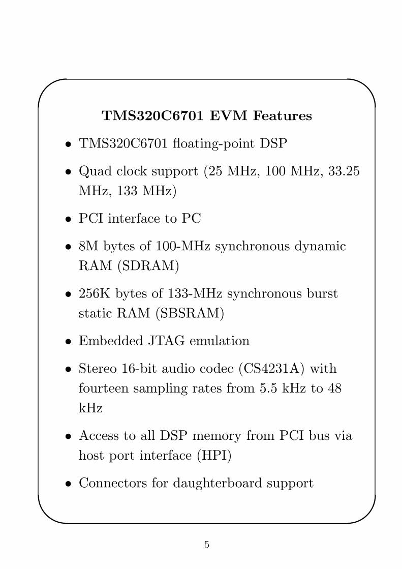
TMS320C6701 EVM Features
• TMS320C6701 floating-point DSP
• Quad clock support (25 MHz, 100 MHz, 33.25
MHz, 133 MHz)
• PCI interface to PC
• 8M bytes of 100-MHz synchronous dynamic
RAM (SDRAM)
• 256K bytes of 133-MHz synchronous burst
static RAM (SBSRAM)
• Embedded JTAG emulation
• Stereo 16-bit audio codec (CS4231A) with
fourteen sampling rates from 5.5 kHz to 48
kHz
• Access to all DSP memory from PCI bus via
host port interface (HPI)
• Connectors for daughterboard support
5
'
&
$
%
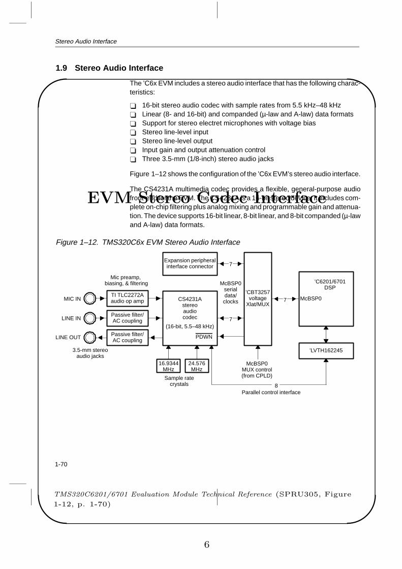
EVM Stereo Codec Interface
Stereo Audio Interface
1-70
1.9 Stereo Audio Interface
The ’C6x EVM includes a stereo audio interface that has the following charac-teristics:
� 16-bit stereo audio codec with sample rates from 5.5 kHz–48 kHz� Linear (8- and 16-bit) and companded (µ-law and A-law) data formats� Support for stereo electret microphones with voltage bias� Stereo line-level input� Stereo line-level output� Input gain and output attenuation control� Three 3.5-mm (1/8-inch) stereo audio jacks
Figure 1–12 shows the configuration of the ’C6x EVM’s stereo audio interface.
The CS4231A multimedia codec provides a flexible, general-purpose audiofront-end for the EVM. The CS4231A is a 16-bit stereo device. It includes com-plete on-chip filtering plus analog mixing and programmable gain and attenua-tion. The device supports 16-bit linear, 8-bit linear, and 8-bit companded (µ-lawand A-law) data formats.
Figure 1–12. TMS320C6x EVM Stereo Audio Interface
’C6201/6701DSP
’CBT3257voltage
Xlat/MUXCS4231A
stereoaudiocodec
(16-bit, 5.5–48 kHz)
TI TLC2272Aaudio op amp
Expansion peripheralinterface connector 7
16.9344MHz
Mic preamp, biasing, & filtering
MIC IN
3.5-mm stereoaudio jacks
Sample ratecrystals
McBSP0
McBSP0MUX control(from CPLD)
McBSP0serialdata/
clocks
PDWN
8
7
7
’LVTH162245
LINE IN
LINE OUT
24.576MHz
Parallel control interface
Passive filter/AC coupling
Passive filter/AC coupling
TMS320C6201/6701 Evaluation Module Technical Reference (SPRU305, Figure
1-12, p. 1-70)
6
'
&
$
%
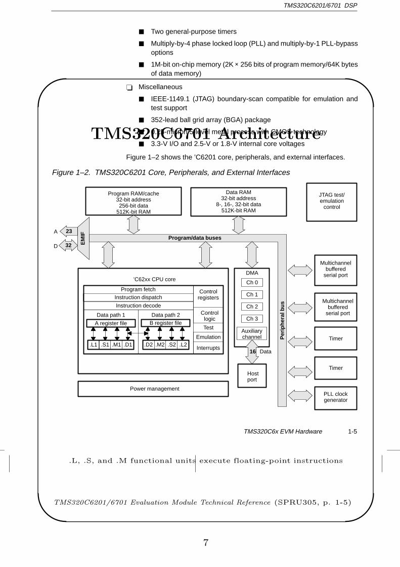
TMS320C6701 Architecture
TMS320C6201/6701 DSP
1-5TMS320C6x EVM Hardware
� Two general-purpose timers
� Multiply-by-4 phase locked loop (PLL) and multiply-by-1 PLL-bypassoptions
� 1M-bit on-chip memory (2K × 256 bits of program memory/64K bytesof data memory)
� Miscellaneous
� IEEE-1149.1 (JTAG) boundary-scan compatible for emulation andtest support
� 352-lead ball grid array (BGA) package
� 0.25-micron/5-level metal process with CMOS technology
� 3.3-V I/O and 2.5-V or 1.8-V internal core voltages
Figure 1–2 shows the ’C6201 core, peripherals, and external interfaces.
Figure 1–2. TMS320C6201 Core, Peripherals, and External Interfaces
A
16 Data
23
D
JTAG test/emulation
control
Power management
Program RAM/cache32-bit address256-bit data
512K-bit RAM
Program/data buses
’C62xx CPU core
Data path 1
.D1.M1.S1.L1
A register file
Data path 2
.L2.S2.M2.D2
B register file
Instruction decode
Instruction dispatchProgram fetch
Interrupts
Controlregisters
Emulation
Test
Controllogic
DMA
Ch 0
Multichannelbuffered
serial port
Multichannelbuffered
serial port
Timer
Timer
PLL clockgenerator
Hostport
Data RAM32-bit address
8-, 16-, 32-bit data512K-bit RAM
Ch 1
Ch 2
Ch 3
Auxiliarychannel P
erip
her
al b
us
EM
IF
32
.L, .S, and .M functional units execute floating-point instructions
TMS320C6201/6701 Evaluation Module Technical Reference (SPRU305, p. 1-5)
7
'
&
$
%
Main ’C6701 Features
• VelociTI Very Long Instruction Word
(VLIW) CPU Core
Fetches eight 32-bit instructions at once
– Eight functional units
∗ Four ALUs (fixed and floating-point)
∗ Two ALUs (fixed-point)
∗ Two multipliers (fixed and
floating-point)
32 × 32 bit integer multiply with 32 or
64-bit result
– Load-store architecture with 32 32-bit
general purpose registers
• Instruction Set Features
– Hardware support for IEEE single and
double precision floating-point operations
– 8, 16, and 32-bit addressable
– 8-bit overflow protection and saturation
– Bit-field extract, set, clear
8
'
&
$
%
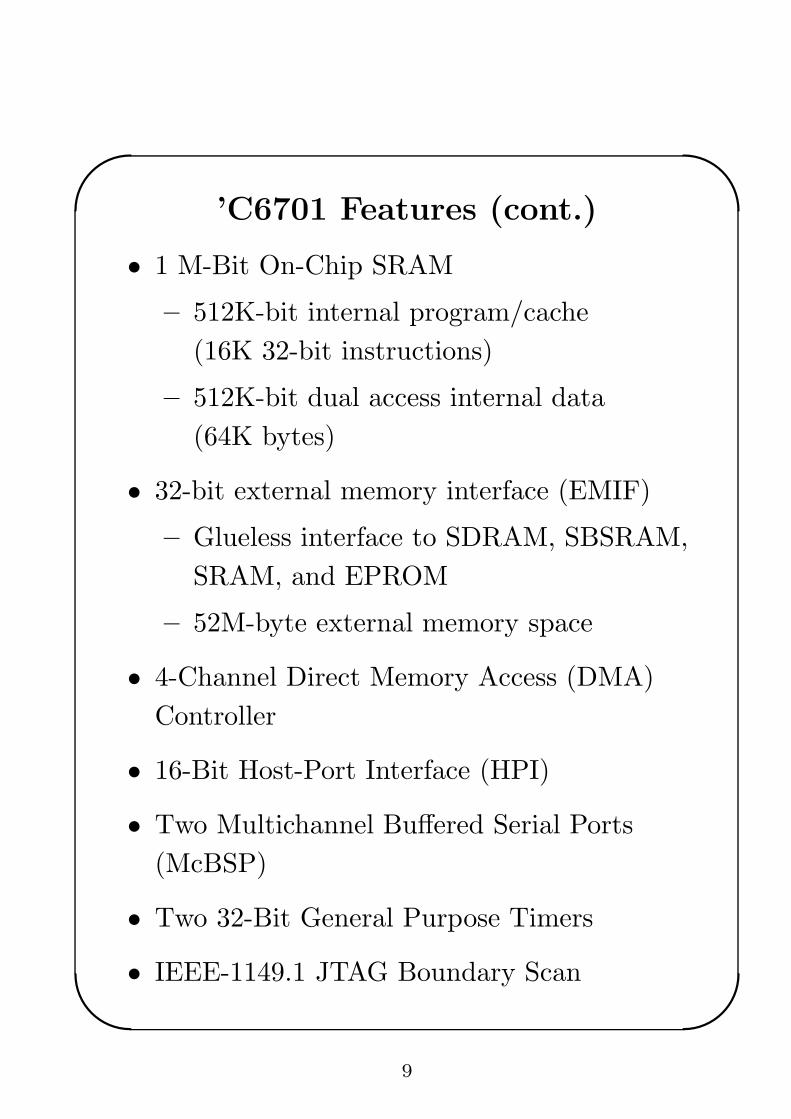
’C6701 Features (cont.)
• 1 M-Bit On-Chip SRAM
– 512K-bit internal program/cache
(16K 32-bit instructions)
– 512K-bit dual access internal data
(64K bytes)
• 32-bit external memory interface (EMIF)
– Glueless interface to SDRAM, SBSRAM,
SRAM, and EPROM
– 52M-byte external memory space
• 4-Channel Direct Memory Access (DMA)
Controller
• 16-Bit Host-Port Interface (HPI)
• Two Multichannel Buffered Serial Ports
(McBSP)
• Two 32-Bit General Purpose Timers
• IEEE-1149.1 JTAG Boundary Scan
9
'
&
$
%
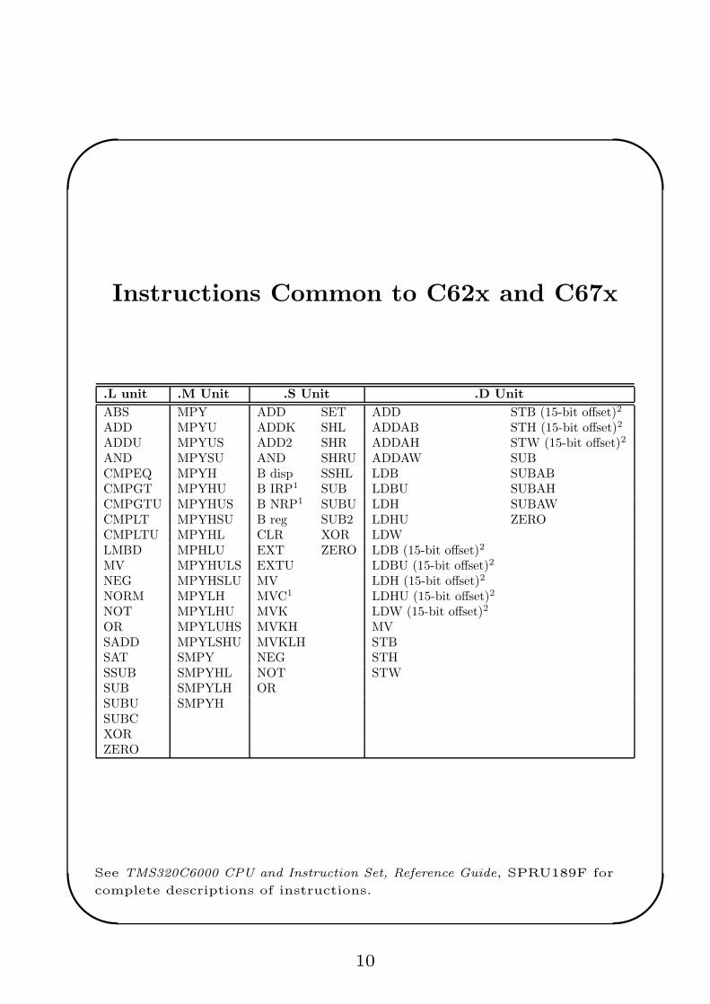
Instructions Common to C62x and C67x
.L unit .M Unit .S Unit .D Unit
ABS MPY ADD SET ADD STB (15-bit offset)2
ADD MPYU ADDK SHL ADDAB STH (15-bit offset)2
ADDU MPYUS ADD2 SHR ADDAH STW (15-bit offset)2
AND MPYSU AND SHRU ADDAW SUBCMPEQ MPYH B disp SSHL LDB SUBABCMPGT MPYHU B IRP1 SUB LDBU SUBAHCMPGTU MPYHUS B NRP1 SUBU LDH SUBAWCMPLT MPYHSU B reg SUB2 LDHU ZEROCMPLTU MPYHL CLR XOR LDWLMBD MPHLU EXT ZERO LDB (15-bit offset)2
MV MPYHULS EXTU LDBU (15-bit offset)2
NEG MPYHSLU MV LDH (15-bit offset)2
NORM MPYLH MVC1 LDHU (15-bit offset)2
NOT MPYLHU MVK LDW (15-bit offset)2
OR MPYLUHS MVKH MVSADD MPYLSHU MVKLH STBSAT SMPY NEG STHSSUB SMPYHL NOT STWSUB SMPYLH ORSUBU SMPYHSUBCXORZERO
See TMS320C6000 CPU and Instruction Set, Reference Guide, SPRU189F for
complete descriptions of instructions.
10
'
&
$
%
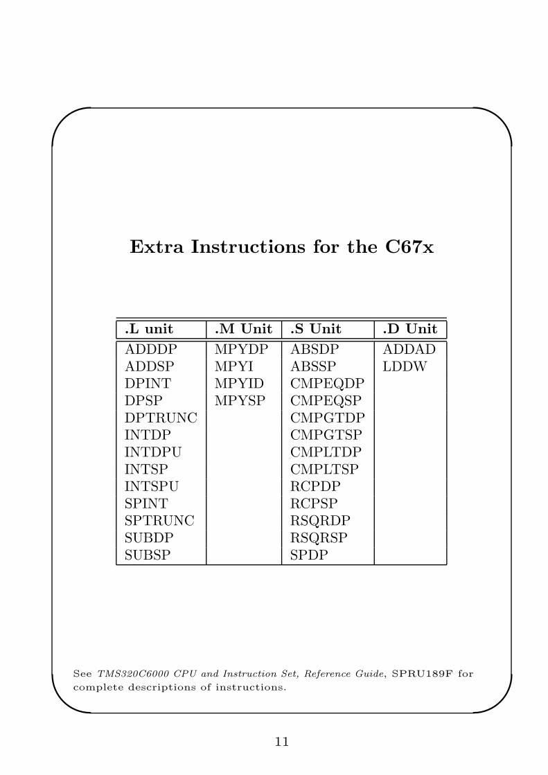
Extra Instructions for the C67x
.L unit .M Unit .S Unit .D Unit
ADDDP MPYDP ABSDP ADDAD
ADDSP MPYI ABSSP LDDW
DPINT MPYID CMPEQDP
DPSP MPYSP CMPEQSP
DPTRUNC CMPGTDP
INTDP CMPGTSP
INTDPU CMPLTDP
INTSP CMPLTSP
INTSPU RCPDP
SPINT RCPSP
SPTRUNC RSQRDP
SUBDP RSQRSP
SUBSP SPDP
See TMS320C6000 CPU and Instruction Set, Reference Guide, SPRU189F for
complete descriptions of instructions.
11
'
&
$
%
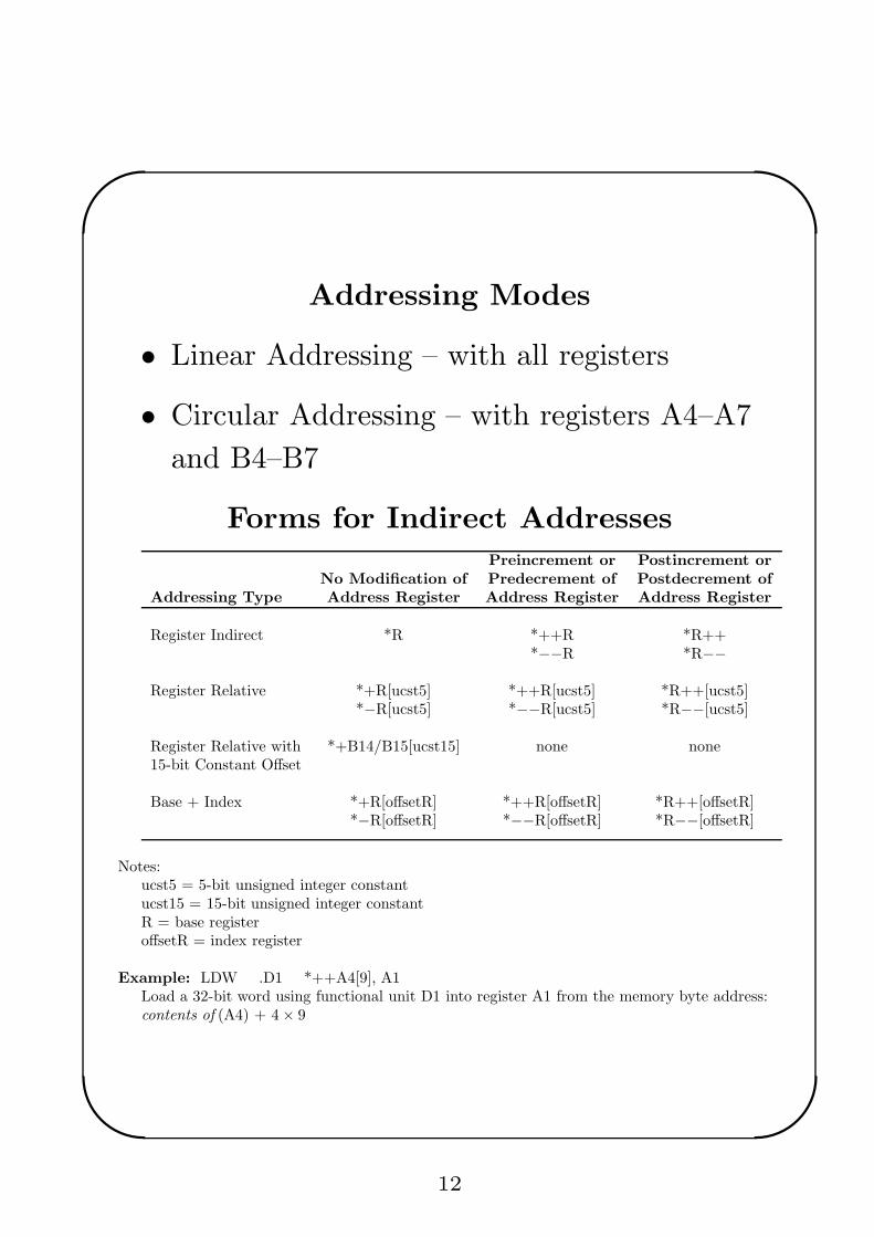
Addressing Modes
• Linear Addressing – with all registers
• Circular Addressing – with registers A4–A7
and B4–B7
Forms for Indirect AddressesPreincrement or Postincrement or
No Modification of Predecrement of Postdecrement of
Addressing Type Address Register Address Register Address Register
Register Indirect *R *++R *R++*−−R *R−−
Register Relative *+R[ucst5] *++R[ucst5] *R++[ucst5]*−R[ucst5] *−−R[ucst5] *R−−[ucst5]
Register Relative with *+B14/B15[ucst15] none none15-bit Constant Offset
Base + Index *+R[offsetR] *++R[offsetR] *R++[offsetR]*−R[offsetR] *−−R[offsetR] *R−−[offsetR]
Notes:ucst5 = 5-bit unsigned integer constantucst15 = 15-bit unsigned integer constantR = base registeroffsetR = index register
Example: LDW .D1 *++A4[9], A1Load a 32-bit word using functional unit D1 into register A1 from the memory byte address:contents of (A4) + 4 × 9
12
'
&
$
%
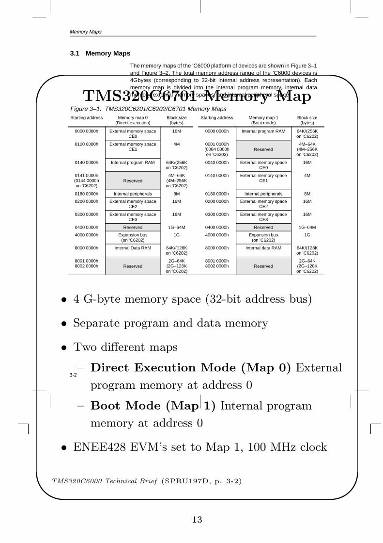
TMS320C6701 Memory Map
Memory Maps
3-2
3.1 Memory Maps
The memory maps of the ’C6000 platform of devices are shown in Figure 3–1and Figure 3–2. The total memory address range of the ’C6000 devices is4Gbytes (corresponding to 32-bit internal address representation). Eachmemory map is divided into the internal program memory, internal datamemory, external memory spaces, and internal peripheral space.
Figure 3–1. TMS320C6201/C6202/C6701 Memory MapsStarting address Memory map 0
(Direct execution)Block size
(bytes)Starting address Memory map 1
(Boot mode)Block size
(bytes)
0000 0000h External memory spaceCE0
16M 0000 0000h Internal program RAM 64K/(256Kon ’C6202)
0100 0000h External memory spaceCE1
4M 0001 0000h(0004 0000hon ’C6202)
Reserved4M–64K
(4M–256Kon ’C6202)
0140 0000h Internal program RAM 64K/(256Kon ’C6202)
0040 0000h External memory spaceCE0
16M
0141 0000h(0144 0000hon ’C6202)
Reserved4M–64K
(4M–256Kon ’C6202)
0140 0000h External memory spaceCE1
4M
0180 0000h Internal peripherals 8M 0180 0000h Internal peripherals 8M
0200 0000h External memory spaceCE2
16M 0200 0000h External memory spaceCE2
16M
0300 0000h External memory spaceCE3
16M 0300 0000h External memory spaceCE3
16M
0400 0000h Reserved 1G–64M 0400 0000h Reserved 1G–64M
4000 0000h Expansion bus(on ’C6202)
1G 4000 0000h Expansion bus(on ’C6202)
1G
8000 0000h Internal Data RAM 64K/(128Kon ’C6202)
8000 0000h Internal data RAM 64K/(128Kon ’C6202)
8001 0000h8002 0000h Reserved
2G–64K(2G–128Kon ’C6202)
8001 0000h8002 0000h Reserved
2G–64K(2G–128Kon ’C6202)
• 4 G-byte memory space (32-bit address bus)
• Separate program and data memory
• Two different maps
– Direct Execution Mode (Map 0) External
program memory at address 0
– Boot Mode (Map 1) Internal program
memory at address 0
• ENEE428 EVM’s set to Map 1, 100 MHz clock
TMS320C6000 Technical Brief (SPRU197D, p. 3-2)
13
'
&
$
%
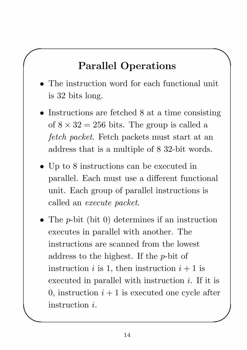
Parallel Operations
• The instruction word for each functional unit
is 32 bits long.
• Instructions are fetched 8 at a time consisting
of 8 × 32 = 256 bits. The group is called a
fetch packet. Fetch packets must start at an
address that is a multiple of 8 32-bit words.
• Up to 8 instructions can be executed in
parallel. Each must use a different functional
unit. Each group of parallel instructions is
called an execute packet.
• The p-bit (bit 0) determines if an instruction
executes in parallel with another. The
instructions are scanned from the lowest
address to the highest. If the p-bit of
instruction i is 1, then instruction i + 1 is
executed in parallel with instruction i. If it is
0, instruction i + 1 is executed one cycle after
instruction i.
14
'
&
$
%
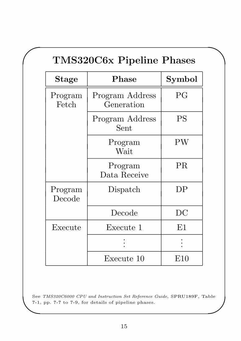
TMS320C6x Pipeline Phases
Stage Phase Symbol
Program Program Address PGFetch Generation
Program Address PSSent
Program PWWait
Program PRData Receive
Program Dispatch DPDecode
Decode DC
Execute Execute 1 E1...
...
Execute 10 E10
See TMS320C6000 CPU and Instruction Set Reference Guide, SPRU189F, Table
7-1, pp. 7-7 to 7-9, for details of pipeline phases.
15
'
&
$
%
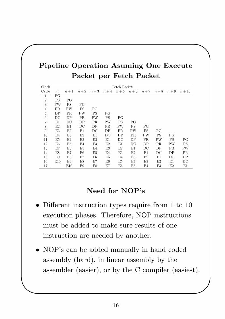
Pipeline Operation Asuming One Execute
Packet per Fetch Packet
Clock Fetch Packet
Cycle n n + 1 n + 2 n + 3 n + 4 n + 5 n + 6 n + 7 n + 8 n + 9 n + 10
1 PG
2 PS PG
3 PW PS PG
4 PR PW PS PG
5 DP PR PW PS PG
6 DC DP PR PW PS PG
7 E1 DC DP PR PW PS PG
8 E2 E1 DC DP PR PW PS PG
9 E3 E2 E1 DC DP PR PW PS PG
10 E4 E3 E2 E1 DC DP PR PW PS PG
11 E5 E4 E3 E2 E1 DC DP PR PW PS PG
12 E6 E5 E4 E3 E2 E1 DC DP PR PW PS
13 E7 E6 E5 E4 E3 E2 E1 DC DP PR PW
14 E8 E7 E6 E5 E4 E3 E2 E1 DC DP PR
15 E9 E8 E7 E6 E5 E4 E3 E2 E1 DC DP
16 E10 E9 E8 E7 E6 E5 E4 E3 E2 E1 DC
17 E10 E9 E8 E7 E6 E5 E4 E3 E2 E1
Need for NOP’s
• Different instruction types require from 1 to 10
execution phases. Therefore, NOP instructions
must be added to make sure results of one
instruction are needed by another.
• NOP’s can be added manually in hand coded
assembly (hard), in linear assembly by the
assembler (easier), or by the C compiler (easiest).
16
'
&
$
%
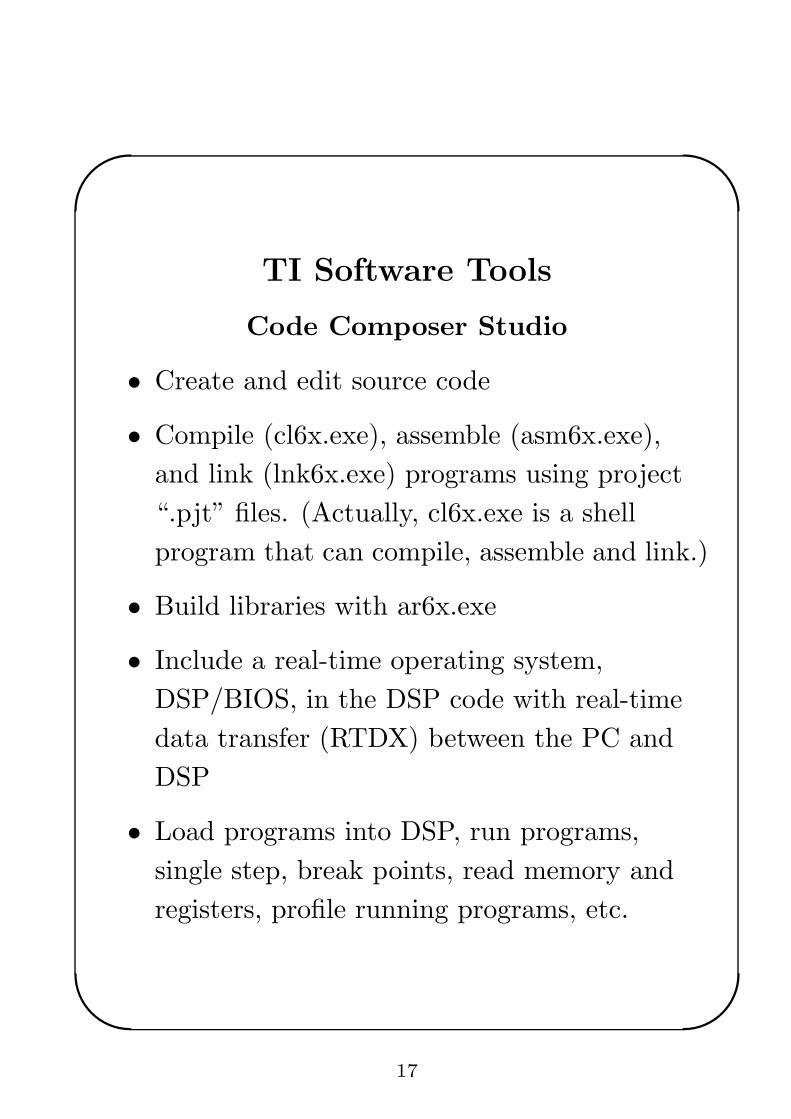
TI Software Tools
Code Composer Studio
• Create and edit source code
• Compile (cl6x.exe), assemble (asm6x.exe),
and link (lnk6x.exe) programs using project
“.pjt” files. (Actually, cl6x.exe is a shell
program that can compile, assemble and link.)
• Build libraries with ar6x.exe
• Include a real-time operating system,
DSP/BIOS, in the DSP code with real-time
data transfer (RTDX) between the PC and
DSP
• Load programs into DSP, run programs,
single step, break points, read memory and
registers, profile running programs, etc.
17
'
&
$
%
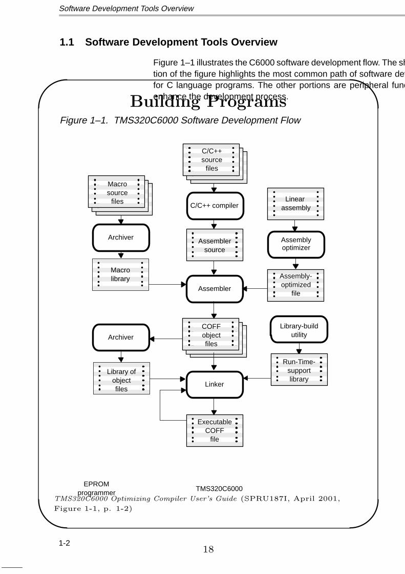
Building Programs
Software Development Tools Overview
1-2
1.1 Software Development Tools Overview
Figure 1–1 illustrates the C6000 software development flow. The shaded por-tion of the figure highlights the most common path of software developmentfor C language programs. The other portions are peripheral functions thatenhance the development process.
Figure 1–1. TMS320C6000 Software Development Flow
Assembler
Linker
Macrolibrary
Library ofobjectfiles
EPROMprogrammer
Assemblersource
COFFobjectfiles
Archiver
Macrosource
files
Archiver
C/C++ compiler
Library-buildutility
Run-Time-supportlibrary
TMS320C6000
C/C++source
files
ExecutableCOFF
file
Assembly-optimized
file
Assemblyoptimizer
Linear assembly
TMS320C6000 Optimizing Compiler User’s Guide (SPRU187I, April 2001,
Figure 1-1, p. 1-2)
18
'
&
$
%
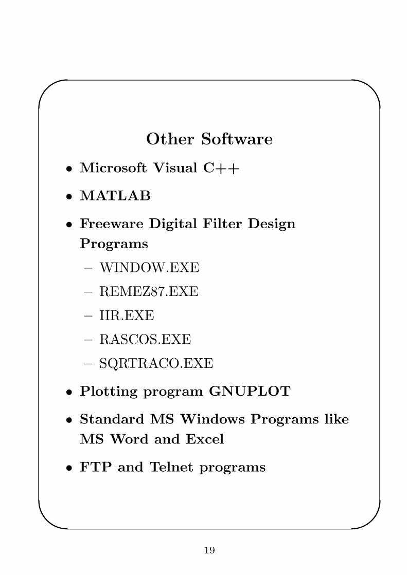
Other Software
• Microsoft Visual C++
• MATLAB
• Freeware Digital Filter Design
Programs
– WINDOW.EXE
– REMEZ87.EXE
– IIR.EXE
– RASCOS.EXE
– SQRTRACO.EXE
• Plotting program GNUPLOT
• Standard MS Windows Programs like
MS Word and Excel
• FTP and Telnet programs
19
'
&
$
%
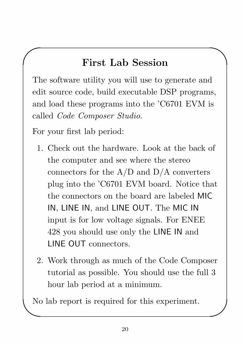
First Lab Session
The software utility you will use to generate and
edit source code, build executable DSP programs,
and load these programs into the ’C6701 EVM is
called Code Composer Studio.
For your first lab period:
1. Check out the hardware. Look at the back of
the computer and see where the stereo
connectors for the A/D and D/A converters
plug into the ’C6701 EVM board. Notice that
the connectors on the board are labeled MIC
IN, LINE IN, and LINE OUT. The MIC IN
input is for low voltage signals. For ENEE
428 you should use only the LINE IN and
LINE OUT connectors.
2. Work through as much of the Code Composer
tutorial as possible. You should use the full 3
hour lab period at a minimum.
No lab report is required for this experiment.
20
'
&
$
%
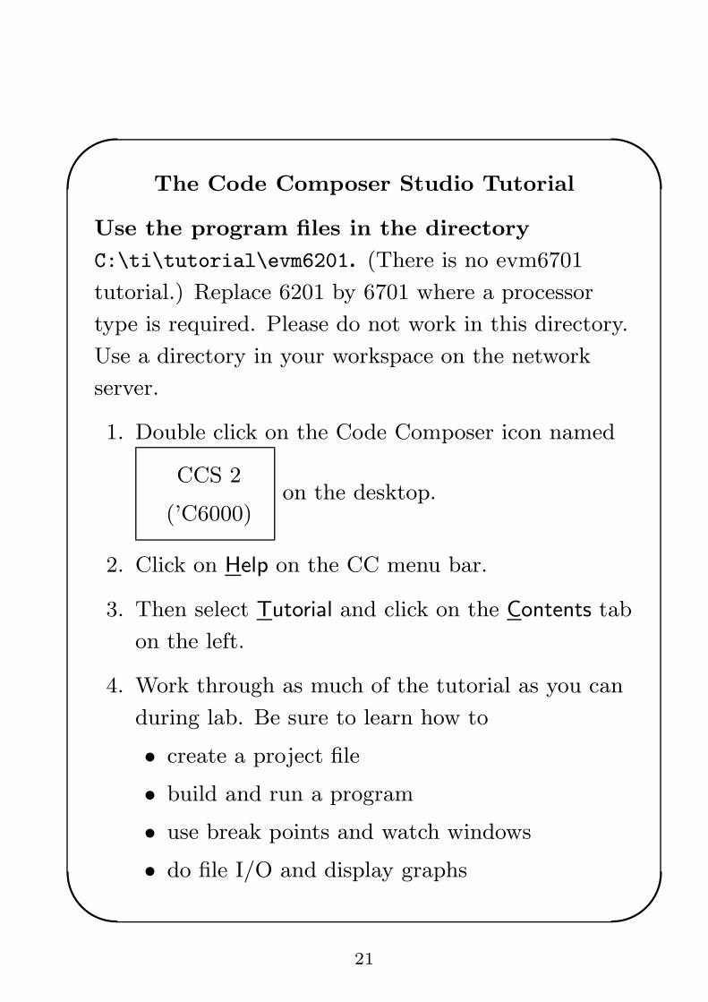
The Code Composer Studio Tutorial
Use the program files in the directory
C:\ti\tutorial\evm6201. (There is no evm6701
tutorial.) Replace 6201 by 6701 where a processor
type is required. Please do not work in this directory.
Use a directory in your workspace on the network
server.
1. Double click on the Code Composer icon named
CCS 2
(’C6000)on the desktop.
2. Click on Help on the CC menu bar.
3. Then select Tutorial and click on the Contents tab
on the left.
4. Work through as much of the tutorial as you can
during lab. Be sure to learn how to
• create a project file
• build and run a program
• use break points and watch windows
• do file I/O and display graphs
21
'
&
$
%
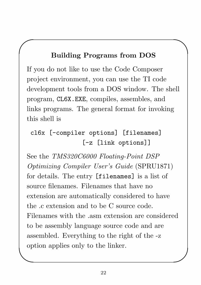
Building Programs from DOS
If you do not like to use the Code Composer
project environment, you can use the TI code
development tools from a DOS window. The shell
program, CL6X.EXE, compiles, assembles, and
links programs. The general format for invoking
this shell is
cl6x [-compiler options] [filenames]
[-z [link options]]
See the TMS320C6000 Floating-Point DSP
Optimizing Compiler User’s Guide (SPRU1871)
for details. The entry [filenames] is a list of
source filenames. Filenames that have no
extension are automatically considered to have
the .c extension and to be C source code.
Filenames with the .asm extension are considered
to be assembly language source code and are
assembled. Everything to the right of the -z
option applies only to the linker.
22