Embed Size (px)
Citation preview

Structural, Optical, and ElectricalProperties of Self-Assembled Films ofPbSe Nanocrystals Treated with1,2-EthanedithiolJoseph M. Luther,†,‡,§ Matt Law,†,§ Qing Song,† Craig L. Perkins,† Matthew C. Beard,† and Arthur J. Nozik†,*†National Renewable Energy Laboratory, Golden, Colorado 80401, and ‡Department of Physics, Colorado School of Mines, Golden, Colorado 80401. §These authorscontributed equally to this work.
Thin films of semiconductor nanoc-rystals (NCs) are emerging as an im-portant class of materials for elec-
tronic and optoelectronic devices such as
field-effect transistors,1–7
photodetectors,8–11 light-emitting
diodes,12–16 metamaterials,17–19 and solar
cells.20,21 The discovery of efficient multiple
exciton generation (MEG) by single pho-
tons in lead chalcogenide NCs22,23 and in
films of electronically coupled NCs24 has ini-
tiated an intense effort to build NC photo-
voltaic devices that exhibit external quan-
tum efficiencies substantially greater than
100% at wavelengths relevant to solar en-
ergy conversion. Calculations show that so-
lar cells utilizing single MEG absorbers can
be up to 44% efficient at one sun, compared
to �33% for cells utilizing conventional ab-
sorbers.25 The potential for high device effi-
ciency and inexpensive fabrication drives
the development of NC solar cells.
Here we describe the structural, optical,
and electrical properties of uniform and
conductive films of PbSe NCs fabricated by
a layer-by-layer (LbL) dip-coating method.
In this method, a monolayer of NCs is de-
posited on a substrate by dip-coating and
then washed in 1,2-ethanedithiol (EDT) in
acetonitrile to remove the electrically insu-
lating oleic acid molecules that originally
solubilize the NCs. Large-area, crack-free NC
films are readily produced by repeating
this procedure until the desired film thick-
ness is attained. We have recently used
these films to construct NC solar cells exhib-
iting large short-circuit current densities
(�24 mA cm�2).26 In order to improve
these devices, we seek a basic understand-
ing of the properties of the EDT-treatedLbL PbSe NC films.
RESULTS AND DISCUSSIONSpin-Cast NC Films. To elucidate the effect
of the EDT treatment on PbSe NC solids,we first prepared a series of 450-nm-thickfilms by spin-coating a 380 mg mL�1 solu-tion of NCs in octane onto various sub-strates. Spin-coating yields NC superlatticescharacterized by strong PbSe 220 texture inwide-angle X-ray scattering (WAXS) pat-terns and multiple sharp reflections insmall-angle X-ray scattering (SAXS) pat-terns, similar to films made by Talapin andMurray by drop-casting.4 As-made NC filmswere compared with films treated in EDTusing Fourier transform infrared (FTIR) spec-troscopy, WAXS and SAXS, X-ray photoelec-tron spectroscopy (XPS), optical absorptionspectroscopy, and scanning electron mi-croscopy (SEM).
Soaking spin-cast NC films in 0.1 M EDTin acetonitrile for several minutes
*Address correspondence [email protected].
Received for review October 29, 2007and accepted January 11, 2008.
Published online January 31, 2008.10.1021/nn7003348 CCC: $40.75
© 2008 American Chemical Society
ABSTRACT We describe the structural, optical, and electrical properties of high-quality films of PbSe
nanocrystals fabricated by a layer-by-layer (LbL) dip-coating method that utilizes 1,2-ethanedithiol (EDT) as an
insolubilizing agent. Comparative characterization of nanocrystal films made by spin-coating and by the LbL
process shows that EDT quantitatively displaces oleic acid on the PbSe surface, causing a large volume loss that
electronically couples the nanocrystals while severely degrading their positional and crystallographic order of the
films. Field-effect transistors based on EDT-treated films are moderately conductive and ambipolar in the dark,
becoming p-type and 30 – 60 times more conductive under 300 mW cm�2 broadband illumination. The nanocrystal
films oxidize rapidly in air to yield, after short air exposures, highly conductive p-type solids. The LbL process
described here is a general strategy for producing uniform, conductive nanocrystal films for applications in
optoelectronics and solar energy conversion.
KEYWORDS: nanocrystals · PbSe · multiple exciton generation · films ·1,2-ethanedithiol · field-effect transistor · oxidation
ARTIC
LE
www.acsnano.org VOL. 2 ▪ NO. 2 ▪ 271–280 ▪ 2008 271

quantitatively removes oleate from the surface of the
nanocrystals (Figure 1).29 This reaction probably occurs
via the nucleophilic attack of oleate by EDT, followed
by Pb�S bond formation and desorption of oleic acid,
or by the dissociative adsorption of EDT on the NC sur-
face to yield adsorbed HS(CH2)2S� and hydrogen,
again followed by desorption of oleic acid (see Figure
S3). As a result of oleate removal, the NCs move closer
together, the NC superlattice becomes disordered, and
the films crack extensively (Figure 2). WAXS shows that
the NC size is unchanged by the EDT treatment (Figure
3). A decrease in the intensity of the PbSe 220 peak in
WAXS patterns indicates that the NCs tilt and rotate as
the layers of NCs within the filmbuckle from the loss of oleate. Weestimate that oleate accounts for30 – 40% of the original filmvolume.
The surface coverage of EDT isfairly high on EDT-treated filmsthat are protected from air. XPSshows substantial sulfur at the filmsurface after exposure to EDT (Fig-ure 4), and the C�H stretch signalin the FTIR spectra is as strong asexpected for quantitative replace-ment of oleate with EDT (Figure 1).The absence of the S�H stretchat �2550 cm�1 suggests that ad-sorbed EDT exists asethanedithiolate31,32 bound in abidentate fashion either on singleNCs or between NCs. Furthermore,the sulfur 2p3/2 X-ray photoelec-tron peak at 161.5 eV is character-istic of bound thiolate rather thanthe free C�S�H moiety.33 XPSdepth profiles measure sulfur inthe film at a concentration of 3.3� 0.35 atom % (Figure S6). Therelatively high coverage of EDT im-
plies that the PbSe NC films might have a low density
of unpassivated surface states. However, our electrical
measurements, discussed below, show that carrier traps
dominate the electrical behavior of the films.
Removal of the insulating oleate and the concomi-
tant decrease in the nanocrystal spacing triggers a
Mott-type insulator-to-conductor transition34 that has
a marked effect on the optical absorption of the spin-
cast films. Figure 5 shows that the EDT treatment causes
the first excitonic transition of the nanocrystals to red-
shift by 86 nm (27 meV). At the same time, absorbance
is enhanced across most of the spectrum such that the
film color changes from a translucent brown, character-
Figure 1. FTIR spectra of 450-nm-thick spin-cast PbSe NC films before and after EDT treatment. (a)The C�H and S�H stretch region. Treated films retain 12–14% of the C�H intensity of untreatedfilms. Quantitative exchange of oleate by EDT would be expected to lower the C�H intensity to ap-proximately 12% of its original intensity (4 C�H bonds in EDT versus 33 C�H bonds in oleic acid). Ex-posing treated films to air for 5 min results in a further 3�6-fold loss of C�H intensity because of de-sorption of EDT (see the section on film oxidation in the text). Note the absence of S�H signal at�2550 cm�1 in the spectrum of the treated films. (b) Survey spectra, acquired in air. The treated, air-exposed film retains only 2% of the C�H signal of the untreated film. Spectra of the as-made PbSefilms are very similar to those of oleate-capped cobalt NCs made by Wu et al.30 At the bottom is a so-dium oleate spectrum for reference. See Figure S5 for reference spectra of EDT and ethanethiol.
Figure 2. Microstructure of the spin-cast NC films before and after EDT treatment. (a) SAXS data, showing a �16 Å decreasein the spacing between the NCs and a dramatic loss of superlattice order upon EDT treatment. Measurements were taken inair. (b,c) Plan-view SEM images of (b) an untreated film and (c) a treated film. Untreated films have a peak-to-valley rough-ness of �75 nm. Scale bars � 1 �m.
ART
ICLE
VOL. 2 ▪ NO. 2 ▪ LUTHER ET AL. www.acsnano.org272

istic of the isolated nanocrystals, to a dull gray. In prin-
ciple, the red-shift and the enhanced absorbance could
arise from changes in (i) the physical or the “electronic”
size35 of the NCs, (ii) the effective dielectric constant at
the surface of the NCs, (iii) radiative electronic coupling
between NCs, and (iv) the degree of wavefunction over-
lap between NCs (i.e., nonradiative electronic cou-
pling).36 The first mechanism is ruled out by our X-ray
diffraction data (Figure 3) and by absorption spectra
showing that no red-shift occurs when oleic acid is re-
placed by octadecanethiol on the surface of the NCs in
solution. To estimate the impact of the second and third
mechanisms, we calculated changes in oscillator
strength and dipole–induced dipole coupling due to
loss of oleate and densification of the NC film (see Sup-
porting Information). Using reasonable assumptions,
we find that the enhanced absorbance is largely ac-
counted for by an increase in the dielectric constant of
the surrounding medium, whereas the red-shift is likely
caused by a combination of strengthened dipole–
induced dipole interactions and wavefunction delocal-
ization, which is consistent with the large increase in DC
conductivity upon EDT treatment (see below).
LbL NC Films. Whereas spin-coating yields disordered
PbSe NC superlattices, LbL dip-coating produces glassy
nanocrystal solids with little translational or crystallo-
graphic order evident by SEM or X-ray scattering. The
NCs pack irregularly in the LbL films and form only small
ordered domains (Figure 6a). The absence of signifi-
cant peaks in SAXS patterns confirms that little
medium-range order exists (Figure 7). Furthermore,
wide-angle scattering patterns of the LbL films re-
semble PbSe powder patterns, indicating that the NCs
are crystallographically isotropic (Figure 7 inset). This is
in contrast to the spin-cast films, which show strong 220
texture. WAXS shows that EDT exposure during the
LbL process does not alter the NC size. In addition, the
LbL films and the spin-cast films have comparable FTIRspectra (Figure S7).
The LbL films and spin-cast films also have similarabsorption spectra. Spectra of LbL films and spin-castfilms of comparable thickness are nearly identical inshape, although the red-shift of the first exciton in theLbL films is usually somewhat smaller (20 –24 meVrather than 24 –27 meV for the spin-cast films; Figure8). The smaller red-shift may reflect the somewhat lessordered and less dense NC packing of the LbL films.
Electrical Measurements. Field-effect transistors (FETs)made from the LbL films and the spin-cast films treatedwith EDT behave identically, showing a dark conductiv-ity of 5 � 10�5 S cm�1 and ambipolar gating (Figure9). Interestingly, the source�drain current of these de-vices, ID, exhibits dramatic time dependence after achange in gate voltage, VG. For example, a positive stepin gate voltage causes ID of the device in Figure 9 tospike and then decay exponentially to near its zero-gate current with a characteristic time constant of 5–7s. Some ID overshoot also occurs. The ID transients asso-ciated with negative steps in VG are well characterizedby two decay constants, 0.5–1.5 s and 9 –13 s. If smallersteps in VG are used, ID decays more quickly and over-shoots less strongly or not at all. Although the exact val-ues of the time constants vary somewhat from deviceto device, the overall behavior was fully reproducibleacross 25 EDT-treated devices prepared by eithermethod. In all cases, the steady-state drain currents areindependent of VG (that is, ID(VG � �30 V) � ID(VG � 30 V) �
ID(VG � 0 V)), as if the gate field is completely screened bymobile charges in the FET channel. The time depen-dence of ID prevents us from determining accurate val-ues for the mobility of carriers in these films. As a checkon the FET substrates and setup, we tested FETs madefrom spin-coated poly(3-hexyl)thiophene (P3HT), a well-characterized hole-conducting polymer.37,38 The P3HTFETs showed stable current switching with changes inVG (Figure S9). This rules out the possibility that prob-lems with the setup (e.g., parasitic gate currents due tolow-quality gate oxide) cause the current transients. In-stead, the transients must result from trap chargingand/or charge redistribution within the NC films or atthe NC/oxide interface in response to steps in the ap-plied gate field.
We modified the surface of the gate oxide in twoways in an effort to stop the ID transients. First, the sub-strates were thoroughly dehydrated prior to NC deposi-tion by heating them to 250 °C for 8 h in a glovebox.This procedure eliminates any surface-bound waterlayer39 that may act to trap charge at the NC/oxide in-terface; such a layer is suspected of causing significantID hysteresis in carbon nanotube FETs and ZnO nano-wire FETs.40–43 However, the use of dehydrated sub-strates had no effect on the ID transients of our PbSeNC FETs. Second, the substrates were treated with hex-amethyldisilazane (HMDS) prior to NC deposition by ex-
Figure 3. WAXS patterns of a spin-cast PbSe NC film beforeand after EDT treatment. Peaks index to rock-salt PbSe. Thediameter of these NCs was determined to be 6.7 nm usingthe Scherrer equation for spherical particles. Measurementswere made in air. A standard PbSe powder diffraction pat-tern is shown at the bottom.
ARTIC
LE
www.acsnano.org VOL. 2 ▪ NO. 2 ▪ 271–280 ▪ 2008 273

posing them to HMDS vapor or liquid at 130 °C for 2 h
in a closed vessel. This procedure replaces the polar
silanol-terminated SiO2 surface with a hydrophobic
trimethylsilyl-terminated surface,44 which should re-
duce the density of charge traps, such as silanol groups
('SiOH), at the silicon oxide surface. An increase in
the contact angle of deionized water from 45 � 5° to
83 � 7° confirmed the efficacy of the HMDS proce-
dure,45 yet using HMDS-treated substrates also did not
affect the ID transients of the PbSe FETs.
We tentatively conclude, on the basis of the totality
of the gate screening and the ineffectiveness of modifi-
cations to the surface of the gate oxide, that the ID tran-
sients are caused by screening of the gate voltage by
charges either injected into the SiO2 itself or trapped on
the layer of NCs immediately adjacent to the oxide sur-
face. Other scenarios, such as charge trapping in the
bulk of the NC film, would screen only part of the field
and probably cannot explain our observations.
The PbSe NC FETs were also measured while illumi-
nated by a broadband tungsten lamp in order to mimic
solar cell operating conditions. At a light intensity of
300 mW cm�2, the films become 30 – 60 times more
conductive and switch from ambipolar to p-type behav-
Figure 4. XPS analysis of untreated (red), EDT-treated (blue), and EDT-treated, air-exposed PbSe NC films (gray). Untreatedfilms were measured without exposure to air. EDT-treated films were treated in 0.1 M EDT for several seconds and measuredwithout exposure to air. Air-exposed films were treated in EDT and then exposed to air for 5 min. Untreated films show oxy-gen peaks at 532.1 and 530.8 eV, assigned to carboxylate oxygen atoms in two different surface-binding modes. The smallcarbon peak at 287.8 eV in the spectrum of the untreated film is assigned to the carboxylate (�COO�) of the adsorbed ole-ate. The simultaneous disappearance of oxygen, reduction of carbon, and enhancement of lead and selenium on EDT-treatedfilms is consistent with removal of the oleate ligand shell. Moreover, EDT-treated films show increased sulfur 2s and 2p sig-nals, indicating that EDT adsorbs to the nanocrystals. Exposure of EDT-treated films to air for several minutes results in theappearance of a large amount of oxygen, small decreases in the lead and selenium signals, and loss of surface sulfur (see thesection on film oxidation in the text). Oxygen peaks at 530.8 and 529.0 eV and the Pb shoulder at high binding energy are in-dicative of Pb(OH)2 and PbOx. A small amount of Se4� is also present, probably as SeO3
2� or SeO2.
ART
ICLE
VOL. 2 ▪ NO. 2 ▪ LUTHER ET AL. www.acsnano.org274

ior, with ION/IOFF � 8 (Figure 10). In addition, the time
constants for ID decay shorten to �1 s for both posi-
tive and negative steps in VG, reflecting the larger num-
ber of free carriers available to fill traps within the illu-
minated films.
Oxidation of the NC Films. EDT-treated films, whether
spin-cast or dip-coated, rapidly oxidize when exposed
to air because the NC surfaces are not well protected by
adsorbed EDT. Brief exposure to air results in the elimi-
nation of EDT from the film surface, as evident in both
the reduction of C�H stretch intensity in FTIR spectra
(Figure 1) and the loss of sulfur signal in XP spectra (Fig-
ure 4). We speculate that the EDT surface complex is hy-
drolyzed in air via the reaction shown in Scheme 1, illus-
trated here with EDT bound in a bidentate
configuration to a single NC.
FTIR spectra indeed show the appearance of a small
O�H band after air exposure, but it seems too weak
for EDT loss to occur exclusively by Scheme 1. A sec-
ond possibility is that adsorbed EDT is oxidized and lost
Figure 5. Optical absorption spectra of a spin-cast film be-fore and after EDT treatment. Spectra were acquired in an in-ert atmosphere using an integrating sphere. A spectrum ofthe nanocrystals in tetrachloroethylene solution is alsoshown. Accurate measurements require that the samplesbe protected from air because the EDT-treated films oxidizein air within minutes (see Figure 12). The full width at half-maximum of the first exciton is 44 meV in each case.
Figure 6. SEM images of PbSe NC films prepared by layer-by-layer dip-coating onto ITO substrates. (a) Plan view. Scalebar � 50 nm. (b) Cross section. Scale bar � 100 nm. All theLbL films studied in this paper were produced using 10 –20dip-coating cycles. See Figure S8 for a large-area SEM view ofa typical film.
Figure 7. SAXS patterns of a typical LbL film and a spin-castfilm treated with EDT. The inset displays the WAXS patterns.A standard PbSe powder diffraction pattern is shown at thebottom.
Figure 8. Optical absorption spectra of a typical LbL PbSeNC film and a spin-cast film before and after EDT treatment,acquired with an integrating sphere in an air-free cell. TheLbL film and EDT-treated spin-cast film are �110 nm thick.The LbL film shows an intermediate red-shift (to 1986 nm,versus 2000 nm for the spin-cast film) and otherwise re-sembles the EDT-treated spin-cast film.
Scheme 1. Hydrolysis of adsorbed ethanedithiolate on PbSe{100}.
ARTIC
LE
www.acsnano.org VOL. 2 ▪ NO. 2 ▪ 271–280 ▪ 2008 275

as a cyclic disulfide rather than the dithiol. XPS analysisof films exposed to air for 5 min reveals that oxygen isbound primarily to lead, probably as a mixture of leadoxides and hydroxides (Figure 4 and Table 1). Smallamounts of SeO3
2� (or SeO2) and a carboxylate spe-cies also appear on the surface. The presence of ad-sorbed water, molecular oxygen, and other species can-not be ruled out by these XPS data. Our results are inagreement with past studies of PbSe surfaceoxidation.46,47
XPS depth profiles reveal that the interior of the NCfilms is significantly different from their outer surface(Figure 11). While the surface of films exposed to air for5 min is devoid of sulfur, their interior contains 1.7 �
0.8 atom % sulfur, about half of the sulfur XP intensitymeasured for films freshly treated with EDT (see FigureS6). Short air exposures therefore do not remove all ofthe EDT adsorbed within the films. Oxygen is foundwithin the air-exposed films at a concentration of 2.7� 1.6 atom %, which is substantially higher than the0.55 � 0.4 atom % oxygen in fresh EDT-treated films but6 times lower than at the surface of air-exposed films.An oxygen-rich surface layer is to be expected on the
basis of simple gas diffusion considerations. Neverthe-
less, the oxygen concentration at depth is probably un-
derestimated because of preferential sputtering of oxy-
gen by the ion beam during depth profiling. Similar
considerations apply to carbon (and maybe sulfur): one
must be cautious in quantifying carbon in depth pro-
files because of the tendency of organic adsorbates to
be damaged and removed from the surface by the sput-
ter beam, resulting in erroneously low carbon concen-
trations. Note that the sulfur loading in the fresh EDT-
treated films may also be underestimated by the depth
profiles. With this caveat in mind, we interpret the null
carbon signal within the film in Figure 11 to mean only
that air exposure reduces the carbon content of the
EDT-treated films (which themselves show only 1.7 �
0.9 atom % carbon, almost certainly an underestimate).
Taken as a whole, the XPS data indicate that air expo-
sure partially removes sulfur and carbon while adding
oxygen, consistent with substantial EDT loss and sur-
face oxidation throughout the air-exposed films.
Oxidation also has a major impact on the optical
and electrical properties of the films. Air exposure re-
sults in a marked blue-shift and weakening of the first
excitonic transition in absorption spectra, indicating a
reduction in inter-NC coupling and NC size (Figure 12a).
Figure 9. Behavior of spin-cast PbSe NC FETs treated withEDT. (a) Time dependence of ID as a function of VG in thedark. The gate voltage was cycled between –30 and �30 Vusing 30 V steps every 3 min. VDS � 10 V. Also shown aredata for the same FET after it was exposed to air for 5 min(see text). Similar behavior is seen with 1 and 10 V steps inVG. (b) Transfer characteristics of the EDT-treated FET, show-ing ambipolar conduction (L � 23 �m, W � 2100 �m, t �75 nm). See Figure S10 for SEM images of this device.
Figure 10. Behavior of a PbSe NC FET under 300 mW cm�2
illumination by a tungsten lamp. (a) Time trace using 30 Vgate voltage steps. (b) Transfer characteristics of the devicein the light (L � 23 �m, W � 2100 �m, t � 60 � 10 nm).
ART
ICLE
VOL. 2 ▪ NO. 2 ▪ LUTHER ET AL. www.acsnano.org276
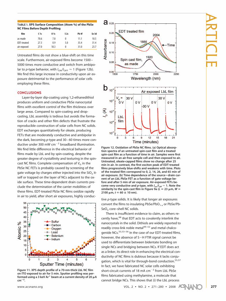
Untreated films do not show a blue-shift on this time
scale. Furthermore, air-exposed films become 1500 –
5000 times more conductive and switch from ambipo-
lar to p-type behavior, with ION/IOFF � 1 (Figure 12b).
We find this large increase in conductivity upon air ex-
posure detrimental to the performance of solar cells
employing these films.
CONCLUSIONSLayer-by-layer dip-coating using 1,2-ethanedithiol
produces uniform and conductive PbSe nanocrystal
films with excellent control of the film thickness over
large areas. Compared to spin-coating and drop-
casting, LbL assembly is tedious but avoids the forma-
tion of cracks and other film defects that frustrate the
reproducible construction of solar cells from NC solids.
EDT exchanges quantitatively for oleate, producing
FETs that are moderately conductive and ambipolar in
the dark, becoming p-type and 30 – 60 times more con-
ductive under 300 mW cm�2 broadband illumination.
We find little difference in the electrical behavior of
films made by LbL and by spin-coating, despite the
greater degree of crystallinity and texturing in the spin-
cast NC films. Complete compensation of VG in the
PbSe NC FETs is probably caused by screening of the
gate voltage by charges either injected into the SiO2 it-
self or trapped on the layer of NCs adjacent to the ox-
ide surface. These time-dependent drain currents pre-
clude the determination of the carrier mobilities of
these films. EDT-treated PbSe NC films oxidize rapidly
in air to yield, after short air exposures, highly conduc-tive p-type solids. It is likely that longer air exposures
convert the films to insulating PbSe/PbO1-x or PbSe/Pb-
SeO3 core–shell NC solids.
There is insufficient evidence to claim, as others re-
cently have,48 that EDT acts to covalently interlink the
nanocrystals in the solid. Dithiols are widely reported to
readily cross-link noble metal49–52 and metal chalco-
genide NCs.35,53–56 In the case of our EDT-treated films,
however, the absence of S�H FTIR signal cannot be
used to differentiate between bidentate bonding on
single NCs and bridging between NCs. If EDT does act
as a linker, its direct role in enhancing the electrical con-
ductivity of NC films is dubious because it lacks conju-
gation, which is vital for through-bond conduction.55,57
In fact, we have fabricated NC solar cells exhibiting
short-circuit currents of 18 mA cm�2 from LbL PbSe
films fabricated using methylamine, a molecule that
cannot bridge NCs. This shows that (i) the LbL process
TABLE 1. XPS Surface Composition (Atom %) of the PbSeNC Films Before Depth Profiling
film C 1s O 1s S 2s Pb 4f Se 3d
as-made 70.6 7.8 0 11.1 10.5EDT-treated 27.3 0.9 5.0 35.4 31.4air-exposed 27.0 18.3 0 31.0 23.7
Figure 11. XPS depth profile of a 70-nm-thick LbL NC filmon ITO exposed to air for 5 min. Sputter profiling was per-formed using a 3 keV Ar� beam at a current density of 20 �Acm�2.
Figure 12. Oxidation of PbSe NC films. (a) Optical absorp-tion spectra of an untreated spin-cast film and a treatedspin-cast film as a function of time in air. Samples were firstmeasured in an air-free sample cell and then exposed to air.Untreated, oleate-capped films show no change after 25min in air. In contrast, the first exciton peak of EDT-treatedfilms progressively blue-shifts and weakens with time. Plotsof the treated film correspond to 0, 2, 14, 26, and 65 min ofair exposure. (b) Time dependence of the source�drain cur-rent of an LbL PbSe FET as a function of gate voltage be-fore and after 5 min of air exposure. Air-exposed FETs be-come very conductive and p-type, with Ion/Ioff � 1. Note thesimilarity to the spin-cast film in Figure 9a (L � 23 �m, W �2100 �m, t � 60 � 10 nm).
ARTIC
LE
www.acsnano.org VOL. 2 ▪ NO. 2 ▪ 271–280 ▪ 2008 277

described here is a general method for producing high-quality NC films for device applications and (ii) themain function of the EDT treatment is probably to de-
crease the inter-NC separation by removing oleate,rather than to provide through-bond conduction be-tween nanocrystals.
METHODSMaterials. Lead oxide (99.999%), selenium (99.99%), oleic acid
(technical grade, 90%), 1-octadecene (ODE, 90%), diphenylphos-phine (DPP, 98%), tetrachloroethylene (TCE, 99.9%), and anhy-drous methanol, acetone, hexane, octane, and acetonitrile werepurchased from Aldrich and used as received. Trioctylphosphine(TOP, technical grade, �90%) and 1,2-ethanedithiol (EDT, �98%)were acquired from Fluka.
PbSe Nanocrystal Synthesis. Standard air-free techniques wereemployed throughout. In a typical synthesis, 0.22 g of PbO wasdissolved in a mixture of 0.73 g of oleic acid and 10 g of ODE at150 °C to yield a clear solution. A mixture of 3 mL of 1 M TOP-Seand 28 mg of DPP was swiftly injected into the solution once itstemperature reached 180 °C, and the temperature was reducedto 155–160 °C to allow the NCs to grow to the desired size. DPP,which enhances the NC yield,27 was used in some but not all ofthe syntheses. The solution was then cooled, 10 mL of hexanewas added, and the NCs were extracted with methanol and pre-cipitated with acetone. Finally, the NCs were washed three timeswith acetone and stored as a powder. The synthesis results inmonodisperse, oleate-capped PbSe nanocrystals that have beencharacterized in detail elsewhere.28 We used several NC samplesin this study, each with an average NC diameter in the range of6 – 8 nm.
Preparation of NC Films by Spin-Coating. All processing occurred ina nitrogen glovebox. PbSe NC films were made by spin-coating�100 L of a 380 mg mL�1 NC solution in octane onto varioussubstrates, such as 1-in. sapphire windows, double-side-polishedintrinsic silicon substrates, glass coated with indium tin oxide(ITO), or degenerate silicon coated with a 110-nm-thick thermaloxide. As-made films were typically 450 nm thick with a peak-to-valley roughness of �75 nm as measured in SEM cross sections.To treat films with EDT, they were immersed in 0.1 M EDT solu-tions in anhydrous acetonitrile for 3 min and blown dry in astream of nitrogen.
Preparation of NC Films by Layer-by-Layer Assembly. All processingoccurred in a helium glovebox. Substrates were dipped by handinto a dilute solution of NCs in hexane (�5 mg mL�1) and thenslowly removed from the solution at a velocity of �0.5 cm s�1.Once dry, substrates were dipped into a beaker containing 0.1 MEDT in anhydrous acetonitrile for several seconds, quickly re-moved, and allowed to dry before repeating the dipping se-quence. Substrates were rotated 90° after each treatment in EDTto ensure film uniformity. Careful dip-coating results in the addi-tion of less than a monolayer of NCs with each step, yieldingsmooth films across several square centimeters. Solutions ofhigher NC concentration tend to deposit thicker NC layers percycle.
Film Characterization. Fourier transform infrared data weretaken on a Nicolet 510 FTIR spectrometer in transmission mode.SAXS and WAXS measurements were carried out with a ScintagX1 diffractometer (Cu K� radiation). A JEOL JSM-7000F field emis-sion scanning electron microscope was used to image the films.Optical absorption data were acquired with a Shimadzu UV-3600spectrophotometer equipped with an integrating sphere. ForXPS analysis, samples were transferred in an inert atmospherefrom the fabrication glovebox to another glovebox integratedwith the ultra-high-vacuum tools, thus avoiding any exposure toair. Films were analyzed “as-prepared” and without any sputtercleaning. Data were obtained on a Physical Electronics 5600 pho-toemission system using monochromatic Al K� radiation and apass energy of 29 eV. The films were found to charge slightly dur-ing analysis, so spectra were aligned by placing the Pb 4f7/2
peak at the lowest observed binding energy of 137.3 eV (seenon the EDT-treated films).
For electrical studies, PbSe NC films were deposited onto de-generately doped silicon substrates coated with a 110-nm-thick
thermal SiO2 gate oxide. Source and drain electrodes (5 nmTi/35 nm Au) spaced 10 –50 m apart were patterned onto theSiO2 surface before NC deposition. When samples were made byspin-coating, two rounds of NC deposition and EDT treatmentwere used to prepare 75-nm-thick films free of through-filmcracks. The portion of each NC film covering the contact padsand touching the underlying silicon substrate (the gate elec-trode) was then removed with a swab. Field-effect measure-ments were performed in a glovebox using a Keithley 236source-measure unit (source�drain) and a Keithley 230 pro-grammable voltage source (gate) driven by Labview software.The noise limit of the setup was �10 pA. The resistance of theuntreated, oleate-capped NC films was always too large to mea-sure with this equipment.
Acknowledgment. We thank S. Shaheen and group for use ofthe fabrication glovebox, L. Gedvilas for assistance with FTIR, M.Page for wafer preparation, J. Chandler for SEM support, and P.Parilla for a kind introduction to SAXS measurements. Funding isprovided by the U.S. Department of Energy, Office of Basic En-ergy Sciences, Division of Chemical Sciences, Biosciences andGeosciences.
Supporting Information Available: Calculations of dielectric ef-fects on film optical properties, reaction schemes for oleate re-moval by EDT, FTIR data on the LbL films and neat EDT/ethaneth-iol, XPS depth profiles, SEM imaging of a PbSe NC FET, and theperformance of P3HT FETs. This material is available free ofcharge via the Internet at http://pubs.acs.org.
REFERENCES AND NOTES1. Ridley, B. A.; Nivi, B.; Jacobson, J. M. All-Inorganic Field
Effect Transistors Fabricated by Printing. Science 1999,286, 746–749.
2. Morgan, N. Y.; Leatherdale, C. A.; Drndic, M.; Jarosz, M. V.;Kastner, M. A.; Bawendi, M. Electronic Transport in Films ofColloidal CdSe Nanocrystals. Phys. Rev. B 2002, 66, 075339.
3. Yu, D.; Wang, C. J.; Guyot-Sionnest, P. n-type ConductingCdSe Nanocrystal Solids. Science 2003, 300, 1277–1280.
4. Talapin, D. V.; Murray, C. B. PbSe Nanocrystal Solids for n-and p-Channel Thin Film Field-Effect Transistors. Science2005, 310, 86–89.
5. Porter, V. J.; Mentzel, T.; Charpentier, S.; Kastner, M. A.;Bawendi, M. G. Temperature-, Gate-, and PhotoinducedConductance of Close-Packed CdTe Nanocrystal Films.Phys. Rev. B 2006, 73, 155303.
6. Urban, J. J.; Talapin, D. V.; Shevchenko, E. V.; Kagan, C. R.;Murray, C. B. Synergism in Binary Nanocrystal SuperlatticesLeads to Enhanced p-type Conductivity in Self-Assembled PbTe/Ag2Te Thin Films. Nat. Mater. 2007, 6,115–121.
7. Kim, H.; Cho, K.; Kim, D. W.; Lee, H. R.; Kim, S. Bottom- andTop-Gate Field-Effect Thin-Film Transistors with pChannels of Sintered HgTe Nanocrystals. Appl. Phys. Lett.2006, 89, 173107.
8. Ginger, D. S.; Greenham, N. C. Charge Injection andTransport in Films of CdSe Nanocrystals. J. Appl. Phys.2000, 87, 1361–1368.
9. Jarosz, M. V.; Porter, V. J.; Fisher, B. R.; Kastner, M. A.;Bawendi, M. G. Photoconductivity Studies of Treated CdSeQuantum Dot Films Exhibiting Increased ExcitonIonization Efficiency. Phys. Rev. B 2004, 70, 195327.
10. Konstantatos, G.; Howard, I.; Fischer, A.; Hoogland, S.;Clifford, J.; Klem, E.; Levina, L.; Sargent, E. H. UltrasensitiveSolution-Cast Quantum Dot Photodetectors. Nature 2006,442, 180–183.
ART
ICLE
VOL. 2 ▪ NO. 2 ▪ LUTHER ET AL. www.acsnano.org278

11. Oertel, D. C.; Bawendi, M. G.; Arango, A. C.; Bulovic, V.Photodetectors Based on Treated CdSe Quantum-DotFilms. Appl. Phys. Lett. 2005, 87, 213505.
12. Artemyev, M. V.; Sperling, V.; Woggon, U.Electroluminescence in Thin Solid Films of Closely PackedCdS Nanocrystals. J. Appl. Phys. 1997, 81, 6975–6977.
13. Bertoni, C.; Gallardo, D.; Dunn, S.; Gaponik, N.; Eychmuller,A. Fabrication and Characterization of Red-EmittingElectroluminescent Devices Based on Thiol-StabilizedSemiconductor Nanocrystals. Appl. Phys. Lett. 2007, 90,034107.
14. Coe, S.; Woo, W. K.; Bawendi, M.; Bulovic, V.Electroluminescence from Single Monolayers ofNanocrystals in Molecular Organic Devices. Nature 2002,420, 800–803.
15. Colvin, V. L.; Schlamp, M. C.; Alivisatos, A. P. Light EmittingDiodes made from Cadmium Selenide Nanocrystals anda Semiconducting Polymer. Nature 1994, 370, 354–357.
16. Gao, M. Y.; Lesser, C.; Kirstein, S.; Mohwald, H.; Rogach,A. L.; Weller, H. Electroluminescence of Different Colorsfrom Polycation/CdTe Nanocrystal Self-Assembled Films.J. Appl. Phys. 2000, 87, 2297–2302.
17. Redl, F. X.; Cho, K. S.; Murray, C. B.; O’Brien, S. Three-Dimensional Binary Superlattices of Magnetic Nanocrystalsand Semiconductor Quantum Dots. Nature 2003, 423,968–971.
18. Shevchenko, E. V.; Talapin, D. V.; Kotov, N. A.; O’Brien, S.;Murray, C. B. Structural Diversity in Binary NanoparticleSuperlattices. Nature 2006, 439, 55–59.
19. Shevchenko, E. V.; Talapin, D. V.; Murray, C. B.; O’Brien, S.Structural Characterization of Self-AssembledMultifunctional Binary Nanoparticle Superlattices. J. Am.Chem. Soc. 2006, 128, 3620–3637.
20. Gur, I.; Fromer, N. A.; Geier, M. L.; Alivisatos, A. P. Air-StableAll-Inorganic Nanocrystal Solar Cells Processed fromSolution. Science 2005, 310, 462–465.
21. Nozik, A. J. Quantum Dot Solar Cells. Phys. E 2002, 14, 115–120.
22. Ellingson, R. J.; Beard, M. C.; Johnson, J. C.; Yu, P. R.; Micic,O. I.; Nozik, A. J.; Shabaev, A.; Efros, A. L. Highly EfficientMultiple Exciton Generation in Colloidal PbSe and PbSQuantum Dots. Nano Lett. 2005, 5, 865–871.
23. Schaller, R. D.; Klimov, V. I. High Efficiency CarrierMultiplication in PbSe Nanocrystals: Implications for SolarEnergy Conversion. Phys. Rev. Lett. 2004, 92, 186601.
24. Luther, J. M.; Beard, M. C.; Song, Q.; Law, M.; Ellingson, R. J.;Nozik, A. J. Multiple Exciton Generation in Films ofElectronically Coupled PbSe Quantum Dots. Nano Lett.2007, 7, 1779–1784.
25. Hanna, M. C.; Nozik, A. J. Solar Conversion Efficiency ofPhotovoltaic and Photoelectrolysis Cells with CarrierMultiplication Absorbers. J. Appl. Phys. 2006, 100, 074510.
26. Luther, J. M.; Law, M.; Song, Q.; Beard, M. C.; Ellingson, R. J.;Nozik, A. J. Manuscript in preparation.
27. Steckel, J. S.; Yen, B. K. H.; Oertel, D. C.; Bawendi, M. G. Onthe Mechanism of Lead Chalcogenide NanocrystalFormation. J. Am. Chem. Soc. 2006, 128, 13032–13033.
28. Murphy, J. E.; Beard, M. C.; Norman, A. G.; Ahrenkiel, S. P.;Johnson, J. C.; Yu, P. R.; Micic, O. I.; Ellingson, R. J.; Nozik,A. J. PbTe Colloidal Nanocrystals: Synthesis,Characterization, and Multiple Exciton Generation. J. Am.Chem. Soc. 2006, 128, 3241–3247.
29. Substantially lower EDT concentrations are equallyeffective, while pure acetonitrile has no effect on the films.See Figure S4, Supporting Information.
30. Wu, N. Q.; Fu, L.; Su, M.; Aslam, M.; Wong, K. C.; Dravid, V. P.Interaction of Fatty Acid Monolayers with CobaltNanoparticles. Nano Lett. 2004, 4, 383–386.
31. Roe, C. L.; Schulz, K. H. Reaction of 1,2-ethanedithiol onClean, Sulfur-Modified, and Carbon-Modified Mo(110)Surfaces. J. Vac. Sci. Technol., A 1998, 16, 1066–1072.
32. Joo, S. W.; Han, S. W.; Kim, K. Multilayer Formation of 1,2-ethanedithiol on Gold: Surface-Enhanced RamanScattering and Ellipsometry Study. Langmuir 2000, 16,5391–5396.
33. Castner, D. G.; Hinds, K.; Grainger, D. W. X-rayPhotoelectron Spectroscopy Sulfur 2p Study of OrganicThiol and Disulfide Binding Interactions with GoldSurfaces. Langmuir 1996, 12, 5083–5086.
34. Remacle, F. On Electronic Properties of Assemblies ofQuantum Nanodots. J. Phys. Chem. A 2000, 104,4739–4747.
35. Koole, R.; Luigjes, B.; Tachiya, M.; Pool, R.; Vlugt, T. J. H.;Donega, C. D. M.; Meijerink, A.; Vanmaekelbergh, D.Differences in Cross-Link Chemistry Between Rigid andFlexible Dithiol Molecules Revealed by Optical Studies ofCdTe Quantum Dots. J. Phys. Chem. C 2007, 111,11208–11215.
36. Schedelbeck, G.; Wegscheider, W.; Bichler, M.; Abstreiter,G. Coupled Quantum Dots Fabricated by Cleaved EdgeOvergrowth: From Artificial Atoms to Molecules. Science1997, 278, 1792–1795.
37. Sirringhaus, H.; Brown, P. J.; Friend, R. H.; Nielsen, M. M.;Bechgaard, K.; Langeveld-Voss, B. M. W.; Spiering, A. J. H.;Janssen, R. A. J.; Meijer, E. W.; Herwig, P.; de Leeuw, D. M.Two-Dimensional Charge Transport in Self-Organized,High-Mobility Conjugated Polymers. Nature 1999, 401,685–688.
38. Kline, R. J.; McGehee, M. D.; Kadnikova, E. N.; Liu, J. S.;Frechet, J. M. J. Controlling the Field-Effect Mobility ofRegioregular Polythiophene by Changing the MolecularWeight. Adv. Mater. 2003, 15, 1519–1522.
39. Zhuravlev, L. T. The Surface Chemistry of AmorphousSilica. Zhuravlev Model. Colloids Surf., A 2000, 173, 1–38.
40. Kim, W.; Javey, A.; Vermesh, O.; Wang, O.; Li, Y. M.; Dai, H. J.Hysteresis Caused by Water Molecules in CarbonNanotube Field-Effect Transistors. Nano Lett. 2003, 3, 193–198.
41. Vijayaraghavan, A.; Kar, S.; Soldano, C.; Talapatra, S.;Nalamasu, O.; Ajayan, P. M. Charge-Injection-InducedDynamic Screening and Origin of Hysteresis in Field-Modulated Transport in Single-Wall Carbon Nanotubes.Appl. Phys. Lett. 2006, 89, 162108.
42. Lee, J. S.; Ryu, S.; Yoo, K.; Choi, I. S.; Yun, W. S.; Kim, J.Origin of Gate Hysteresis in Carbon Nanotube Field-EffectTransistors. J. Phys. Chem. C 2007, 111, 12504–12507.
43. Goldberger, J.; Sirbuly, D. J.; Law, M.; Yang, P. ZnONanowire Transistors. J Phys. Chem. B 2005, 109, 9–14.
44. Hertl, W.; Hair, M. L. Reaction of Hexamethyldisilazane withSilica. J. Phys. Chem. 1971, 75, 2181–2185.
45. Lim, S. C.; Kim, S. H.; Lee, J. H.; Kim, M. K.; Kim, D. J.; Zyung,T. Surface-Treatment Effects on Organic Thin-FilmTransistors. Synth. Met. 2005, 148, 75–79.
46. Gautier, C.; Cambon-Muller, M.; Averous, M. Study of PbSeLayer Oxidation and Oxide Dissolution. Appl. Surf. Sci.1999, 141, 157–163.
47. Sarkar, S. K.; Kababya, S.; Vega, S.; Cohen, H.; Woicik, J. C.;Frenkel, A. I.; Hodes, G. Effects of Solution pH and SurfaceChemistry on the Postdeposition Growth of Chemical BathDeposited PbSe Nanocrystalline Films. Chem. Mater. 2007,19, 879–888.
48. Klem, E. J. D.; MacNeil, D. D.; Cyr, P. W.; Levina, L.; Sargent,E. H. Efficient Solution-Processed Infrared PhotovoltaicCells: Planarized All-Inorganic Bulk Heterojunction Devicesvia Inter-Quantum-Dot Bridging during Growth fromSolution. Appl. Phys. Lett. 2007, 90, 183113.
49. Leibowitz, F. L.; Zheng, W. X.; Maye, M. M.; Zhong, C. J.Structures and Properties of Nanoparticle Thin FilmsFormed via a One-Step Exchange-Cross-Linking�Precipitation Route. Anal. Chem. 1999, 71, 5076–5083.
50. Ahonen, P.; Laaksonen, T.; Nykanen, A.; Ruokolainen, J.;Kontturi, K. Formation of Stable Ag-NanoparticleAggregates Induced by Dithiol Cross-Linking. J. Phys.Chem. B 2006, 110, 12954–12958.
51. Brust, M.; Bethell, D.; Schiffrin, D. J.; Kiely, C. J. Novel Gold-Dithiol Nano-Networks with Nonmetallic ElectronicProperties. Adv. Mater. 1995, 7, 795–797.
ARTIC
LE
www.acsnano.org VOL. 2 ▪ NO. 2 ▪ 271–280 ▪ 2008 279

52. Zabet-Khosousi, A.; Trudeau, P. E.; Suganuma, Y.; Dhirani,A. A.; Statt, B. Metal to Insulator Transition in Films ofMolecularly Linked Gold Nanoparticles. Phys. Rev. Lett.2006, 96, 156403.
53. Koole, R.; Liljeroth, P.; Donega, C. D.; Vanmaekelbergh, D.;Meijerink, A. Electronic Coupling and Exciton EnergyTransfer in CdTe Quantum-Dot Molecules. J. Am. Chem.Soc. 2006, 128, 10436–10441.
54. Pacifico, J.; Jasieniak, J.; Gomez, D. E.; Mulvaney, P. Tunable3-D Arrays of Quantum Dots: Synthesis and LuminescenceProperties. Small 2006, 2, 199–203.
55. Ouyang, M.; Awschalom, D. D. Coherent Spin Transferbetween Molecularly Bridged Quantum Dots. Science2003, 301, 1074–1078.
56. Torimoto, T.; Tsumura, N.; Nakamura, H.; Kuwabata, S.;Sakata, T.; Mori, H.; Yoneyama, H. PhotoelectrochemicalProperties of Size-Quantized SemiconductorPhotoelectrodes Prepared by Two-Dimensional Cross-Linking of Monodisperse CdS Nanoparticles. Electrochim.Acta 2000, 45, 3269–3276.
57. Schrier, J.; Whaley, K. B. Atomistic Theory of Coherent SpinTransfer between Molecularly Bridged Quantum Dots.Phys. Rev. B 2005, 72, 085320.
ART
ICLE
VOL. 2 ▪ NO. 2 ▪ LUTHER ET AL. www.acsnano.org280
![SAXS SAXS/WAXS WAXS DATA REDUCTION...¾ The Time to Digital Converter (VTDC4) [5] plays a very important role in the whole acquisition system, since it receives signals from the detector](https://img.pdfslide.net/doc/110x75/5ea88ffffbfd6358b71c4c1b/saxs-saxswaxs-waxs-data-the-time-to-digital-converter-vtdc4-5-plays.jpg)